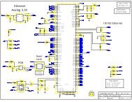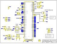
ADC chip Datasheet - Technologic Systems
ADC chip Datasheet - Technologic Systems
ADC chip Datasheet - Technologic Systems

Create successful ePaper yourself
Turn your PDF publications into a flip-book with our unique Google optimized e-Paper software.
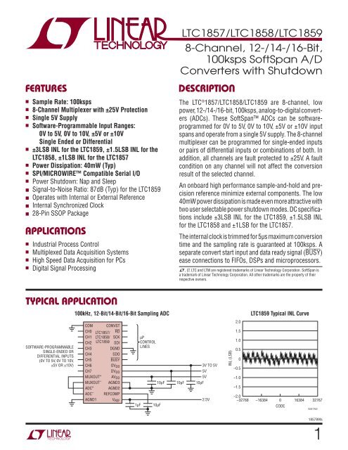
FEATURESn Sample Rate: 100kspsn 8-Channel Multiplexer with ±25V Protectionn Single 5V Supplyn Software-Programmable Input Ranges:0V to 5V, 0V to 10V, ±5V or ±10VSingle Ended or Differentialn ±3LSB INL for the LTC1859, ±1.5LSB INL for theLTC1858, ±1LSB INL for the LTC1857n Power Dissipation: 40mW (Typ)n SPI/MICROWIRE Compatible Serial I/On Power Shutdown: Nap and Sleepn Signal-to-Noise Ratio: 87dB (Typ) for the LTC1859n Operates with Internal or External Referencen Internal Synchronized Clockn 28-Pin SSOP PackageAPPLICATIONSn Industrial Process Controln Multiplexed Data Acquisition <strong>Systems</strong>n High Speed Data Acquisition for PCsn Digital Signal ProcessingLTC1857/LTC1858/LTC18598-Channel, 12-/14-/16-Bit,100ksps SoftSpan A/DConverters with ShutdownDESCRIPTIONThe LTC ® 1857/LTC1858/LTC1859 are 8-channel, lowpower, 12-/14-/16-bit, 100ksps, analog-to-digital converters(<strong>ADC</strong>s). These SoftSpan <strong>ADC</strong>s can be softwareprogrammedfor 0V to 5V, 0V to 10V, ±5V or ±10V inputspans and operate from a single 5V supply. The 8-channelmultiplexer can be programmed for single-ended inputsor pairs of differential inputs or combinations of both. Inaddition, all channels are fault protected to ±25V. A faultcondition on any channel will not affect the conversionresult of the selected channel.An onboard high performance sample-and-hold and precisionreference minimize external components. The low40mW power dissipation is made even more attractive withtwo user selectable power shutdown modes. DC specificationsinclude ±3LSB INL for the LTC1859, ±1.5LSB INLfor the LTC1858 and ±1LSB for the LTC1857.The internal clock is trimmed for 5μs maximum conversiontime and the sampling rate is guaranteed at 100ksps. Aseparate convert start input and data ready signal (BUSY)ease connections to FIFOs, DSPs and microprocessors.L, LT, LTC and LTM are registered trademarks of Linear Technology Corporation. SoftSpan isa trademark of Linear Technology Corporation. All other trademarks are the property of theirrespective owners.TYPICAL APPLICATION100kHz, 12-Bit/14-Bit/16-Bit Sampling <strong>ADC</strong>LTC1859 Typical INL CurveSOFTWARE-PROGRAMMABLESINGLE-ENDED ORDIFFERENTIAL INPUTS(0V TO 5V, 0V TO 10V,±5V OR ±10V)COMCH0CH1CH2CH3CH4CH5CH6CH7MUXOUT +MUXOUT –<strong>ADC</strong> +<strong>ADC</strong> –AGND1CONVSTRDSCKSDIDGNDSDOBUSYOV DDDV DDAV DDAGND3AGND2REFCOMPV REFLTC1857/LTC1858/LTC18591μFμPCONTROLLINES10μF10μF10μF10μF3V TO 5V5V5V2.5VINL (LSB)2.01.51.00.50–0.5–1.0–1.5–2.0–32768–16384 0 16384 32767CODE1859 TA02185789fa1
LTC1857/LTC1858/LTC1859ABSOLUTE MAXIMUM RATINGS(Note 1)Supply Voltage (OV DD = DV DD = AV DD = V DD ) .............6VGround Voltage DifferenceDGND, AGND1, AGND2, AGND3 ........................±0.3VAnalog Input Voltage<strong>ADC</strong> + , <strong>ADC</strong> –(Note 3) ................. (AGND1 – 0.3V) to (AV DD + 0.3V)CH0-CH7, COM ..................................................±25VDigital Input Voltage (Note 4) .......(DGND – 0.3V) to 10VDigital Output Voltage ..(DGND – 0.3V) to (DV DD + 0.3V)Power Dissipation ...............................................500mWOperating Temperature RangeLTC1857C/LTC1858C/LTC1859C .............. 0°C to 70°CLTC1857I/LTC1858I/LTC1859I .............. –40°C to 85°CStorage Temperature Range ................... –65°C to 150°CLead Temperature (Soldering, 10 sec) .................. 300°CPIN CONFIGURATIONTOP VIEWCOMCH0CH1CH2CH3CH4CH5CH6CH7MUXOUT +MUXOUT –<strong>ADC</strong> +<strong>ADC</strong> –AGND112345678910111213142827262524232221201918171615CONVSTRDSCKSDIDGNDSDOBUSYOV DDDV DDAV DDAGND3AGND2REFCOMPV REFG PACKAGE28-LEAD PLASTIC SSOPT JMAX = 110°C, θ JA = 95°C/WORDER INFORMATIONLEAD FREE FINISH TAPE AND REEL PART MARKING PACKAGE DESCRIPTION TEMPERATURE RANGELTC1857CG#PBF LTC1857CG#TRPBF 28-Lead Plastic SSOP 0°C to 70°CLTC1857IG#PBF LTC1857IG#TRPBF 28-Lead Plastic SSOP –40°C to 85°CLTC1858CG#PBF LTC1858CG#TRPBF 28-Lead Plastic SSOP 0°C to 70°CLTC1858IG#PBF LTC1858IG#TRPBF 28-Lead Plastic SSOP –40°C to 85°CLTC1859CG#PBF LTC1859CG#TRPBF 28-Lead Plastic SSOP 0°C to 70°CLTC1859IG#PBF LTC1859IG#TRPBF 28-Lead Plastic SSOP –40°C to 85°CLEAD BASED FINISH TAPE AND REEL PART MARKING PACKAGE DESCRIPTION TEMPERATURE RANGELTC1857CG LTC1857CG#TR 28-Lead Plastic SSOP 0°C to 70°CLTC1857IG LTC1857IG#TR 28-Lead Plastic SSOP –40°C to 85°CLTC1858CG LTC1858CG#TR 28-Lead Plastic SSOP 0°C to 70°CLTC1858IG LTC1858IG#TR 28-Lead Plastic SSOP –40°C to 85°CLTC1859CG LTC1859CG#TR 28-Lead Plastic SSOP 0°C to 70°CLTC1859IG LTC1859IG#TR 28-Lead Plastic SSOP –40°C to 85°CConsult LTC Marketing for parts specifi ed with wider operating temperature ranges.For more information on lead free part marking, go to: http://www.linear.com/leadfree/For more information on tape and reel specifi cations, go to: http://www.linear.com/tapeandreel/2185789fa
LTC1857/LTC1858/LTC1859CONVERTER AND MULTPLEXER CHARACTERISTICS The l denotes the specifications whichapply over the full operating temperature range, otherwise specifications are at T A = 25°C. MUXOUT connected to <strong>ADC</strong> inputs. (Notes 5, 6)LTC1857 LTC1858 LTC1859PARAMETERCONDITIONSMIN TYP MAX MIN TYP MAX MIN TYP MAX UNITSResolution l 12 14 16 BitsNo Missing Codes l 12 14 15 BitsTransition Noise 0.06 0.26 1 LSB RMSIntegral Linearity Error (Notes 7, 15) l ±1 ±1.5 ±3 LSBDifferential Linearity Error (Note 15) l –1 1 –1 1.5 –2 4 LSBBipolar Zero Error (Note 8) l ±9 ±17 ±28 LSBBipolar Zero Error Drift ±0.1 ±0.1 ±0.1 ppm/°CBipolar Zero Error Match ±4 ±6 ±10 LSBUnipolar Zero Error (Note 8) l ±6 ±15 ±25 LSBUnipolar Zero Error Drift ±1 ±1 ±1 ppm/°CUnipolar Zero Error Match ±1.2 ±2 ±8 LSBBipolar Full-Scale Error External Reference (Note 11)Internal Reference (Note 11)Bipolar Full-Scale Error Drift External ReferenceInternal Referencel ±0.35±0.45±2.5±7±2.5±7±0.15±0.4±2.5±7±0.1±0.4%%ppm/°Cppm/°CBipolar Full-Scale Error Match ±5 ±10 ±15 LSBUnipolar Full-Scale Error External Reference (Note 11)Internal Reference (Note 11)Unipolar Full-Scale Error Drift External ReferenceInternal Referencel ±0.45±0.75±2.5±7±2.5±7±0.25±0.85±2.5±7±0.2±0.75%%ppm/°Cppm/°CUnipolar Full-Scale Error Match ±5 ±12 ±15 LSBInput Common Mode Range Unipolar ModeBipolar Modell0 to 10±100 to 10±100 to 10±10VVInput Common Mode Rejection Ratio 96 96 96 dBANALOG INPUT The l denotes the specifi cations which apply over the full operating temperature range, otherwisespecifi cations are at T A = 25°C. (Note 5)PARAMETER CONDITIONS MIN TYP MAX UNITSAnalog Input Range CH0 to CH7, COM 0 to 5, 0 to 10±5, ±10<strong>ADC</strong> + , <strong>ADC</strong> – (Note 3) 0 to 2.0480 to 4.096<strong>ADC</strong> – ±1.024<strong>ADC</strong> – ±2.048ImpedanceCH0 to CH7, COMUnipolarBipolarMUXOUT + , MUXOUT –UnipolarBipolar<strong>ADC</strong> + , <strong>ADC</strong> – Hi-Z kΩCapacitance CH0 to CH7, COM 5 pFSample Mode <strong>ADC</strong> + , <strong>ADC</strong> –0V to 2.048V, ±1.024V0V to 4.096V, ±2.048VHold Mode <strong>ADC</strong> + , <strong>ADC</strong> – 4 pFInput Leakage Current <strong>ADC</strong> + , <strong>ADC</strong> – , CONVST = Low l ±1 μA42311052412VVVVVVkΩkΩkΩkΩpFpF185789fa3
LTC1857/LTC1858/LTC1859DYNAMIC ACCURACYThe l denotes the specifi cations which apply over the full operating temperature range,otherwise specifi cations are at T A = 25°C. MUXOUT connected to <strong>ADC</strong> inputs. (Notes 5, 12)SYMBOL PARAMETER CONDITIONSMIN TYP MAX MIN TYP MAX MIN TYP MAX UNITSS/(N + D) Signal-to-(Noise + Distortion) Ratio 1kHz Input Signal 74 83 87 dBTHD Total Harmonic Distortion 1kHz Input Signal,–101 –101 –101 dBFirst Five HarmonicsPeak Harmonic or Spurious Noise 1kHz Input Signal –103 –103 –103 dBChannel-to-Channel Isolation 1kHz Input Signal –120 –120 –120 dB–3dB Input Bandwidth 1 1 1 MHzAperture Delay –70 –70 –70 nsAperture Jitter 60 60 60 psTransient ResponseFull-Scale Step4 4 4 μs(Note 9)Overvoltage Recovery (Note 13) 150 150 150 ns4LTC1857 LTC1858 LTC1859INTERNAL REFERENCE CHARACTEERISTICS The l denotes the specifi cations which apply over thefull operating temperature range, otherwise specifi cations are at T A = 25°C. (Note 5)PARAMETER CONDITIONS MIN TYP MAX UNITSV REF Output Voltage I OUT = 0 l 2.475 2.5 2.525 VV REF Output Temperature Coeffi cient I OUT = 0 ±10 ppm/°CV REF Output Impedance –0.1mA ≤ I OUT ≤ 0.1mA 8 kΩV REFCOMP Output Voltage I OUT = 0 4.096 VDIGITAL INPUTS AND DIGITAL OUTPUTS The l denotes the specifi cations which apply over thefull operating temperature range, otherwise specifi cations are at T A = 25°C. (Note 5)SYMBOL PARAMETER CONDITIONS MIN TYP MAX UNITSV IH High Level Input Voltage V DD = 5.25V l 2.4 VV IL Low Level Input Voltage V DD = 4.75V l 0.8 VI IN Digital Input Current V IN = 0V to V DD l ±10 μAC IN Digital Input Capacitance 5 pFV OH High Level Output Voltage V DD = 4.75V, I O = –10μA, OV DD = V DD4.74 VV DD = 4.75V, I O = –200μA, OV DD = V DD l 4VV OL Low Level Output Voltage V DD = 4.75V, I O = 160μA, OV DD = V DD0.05VV DD = 4.75V, I O = 1.6mA, OV DD = V DDl0.10 0.4VI OZ Hi-Z Output Leakage V OUT = 0V to V DD , RD = High l ±10 μAC OZ Hi-Z Output Capacitance RD = High 15 pFI SOURCE Output Source Current V OUT = 0V –10 mAI SINK Output Sink Current V OUT = V DD 10 mAPOWER REQUIREMENTS The l denotes the specifi cations which apply over the full operating temperaturerange, otherwise specifi cations are at T A = 25°C. (Note 5)PARAMETER CONDITIONS MIN TYP MAX UNITSPositive Supply Voltage (Notes 9 and 10) 4.75 5 5.25 VPositive Supply CurrentNap ModeSleep ModePower DissipationNap ModeSleep ModeCONVST = 0V or 5VCONVST = 0V or 5Vl 85.584027.54013 8 15 mAmW185789fa
LTC1857/LTC1858/LTC1859TIMING CHARACTERISTICS The l denotes the specifi cations which apply over the full operating temperaturerange, otherwise specifi cations are at T A = 25°C. (Note 5)SYMBOL PARAMETER CONDITIONS MIN TYP MAX UNITSf SAMPLE(MAX) Maximum Sampling Frequency Through CH0 to CH7 Inputsl 100kHzThrough <strong>ADC</strong> + , <strong>ADC</strong> – Only166kHzt CONV Conversion Time l 4 5 μst ACQ Acquisition Time Through CH0 to CH7 Inputsl4 μsThrough <strong>ADC</strong> + , <strong>ADC</strong> – Only1μsf SCK SCK Frequency (Note 14) l 0 20 MHzt r SDO Rise Time See Test Circuits 6 nst f SDO Fall Time See Test Circuits 6 nst 1 CONVST High Time l 40 nst 2 CONVST to BUSY Delay C L = 25pF, See Test Circuits l 15 30 nst 3 SCK Period l 50 nst 4 SCK High l 10 nst 5 SCK Low l 10 nst 6 Delay Time, SCK↓ to SDO Valid C L = 25pF, See Test Circuits l 25 45 nst 7Time from Previous SDO Data Remains C L = 25pF, See Test Circuits l 5 20 nsValid After SCK↓t 8 SDO Valid After RD↓ C L = 25pF, See Test Circuits l 11 30 nst 9 RD↓ to SCK Setup Time l 20 nst 10 SDI Setup Time Before SCK↑ l 0 nst 11 SDI Hold Time After SCK↑ l 7 nst 12 SDO Valid Before BUSY↑ RD = Low, C L = 25pF, See Test Circuits l 5 20 nst 13 Bus Relinquish Time See Test Circuits l 10 30 nsNote 1: Stresses beyond those listed under Absolute Maximum Ratingsmay cause permanent damage to the device. Exposure to any AbsoluteMaximum Rating condition for extended periods may affect devicereliability and lifetime.Note 2: All voltage values are with respect to ground with DGND, AGND1,AGND2 and AGND3 wired together unless otherwise noted.Note 3: When these pin voltages are taken below ground or above AV DD =DV DD = OV DD = V DD , they will be clamped by internal diodes. This productcan handle currents of greater than 100mA below ground or above V DDwithout latchup.Note 4: When these pin voltages are taken below ground they will beclamped by internal diodes. This product can handle currents of greaterthan 100mA below ground without latchup. These pins are not clampedto V DD .Note 5: V DD = 5V, f SAMPLE = 100kHz, t r = t f = 5ns unless otherwisespecified.Note 6: Linearity, offset and full-scale specifi cations apply for a singleendedanalog MUX input with respect to ground or <strong>ADC</strong> + with respect to<strong>ADC</strong> – tied to ground.Note 7: Integral nonlinearity is defi ned as the deviation of a code from astraight line passing through the actual end points of the transfer curve.The deviation is measured from the center of the quantization band.Note 8: Bipolar zero error is the offset voltage measured from –0.5LSBwhen the output code fl ickers between 0000 0000 0000 0000 and 11111111 1111 1111 for the LTC1859, between 00 0000 0000 0000 and 111111 1111 1111 for the LTC1858 and between 0000 0000 0000 and1111 1111 1111 for the LTC1857. Unipolar zero error is the offset voltagemeasured from 0.5LSB when the output codes fl icker between 0000 00000000 0000 and 0000 0000 0000 0001 for the LTC1859, between 00 00000000 0000 and 00 0000 0000 0001 for the LTC1858 and between 00000000 0000 and 0000 0000 0001 for the LTC1857.Note 9: Guaranteed by design, not subject to test.Note 10: Recommended operating conditions.Note 11: Full-scale bipolar error is the worst case of –FS or +FSuntrimmed deviation from ideal fi rst and last code transitions, divided bythe full-scale range, and includes the effect of offset error. For unipolarfull-scale error, the deviation of the last code transition from ideal, dividedby the full-scale range, and includes the effect of offset error.Note 12: All Specifi cations in dB are referred to a full-scale ±10V input.Note 13: Recovers to specifi ed performance after (2 • FS) inputovervoltage.Note 14: t 6 of 45ns maximum allows f SCK up to 10MHz for rising capturewith 50% duty cycle and f SCK up to 20MHz for falling capture (with 5nssetup time for the receiving logic).Note 15: The specifi cation is referred to the ±10V input range.185789fa5
LTC1857/LTC1858/LTC1859TYPICAL PERFORMANCE CHARACTERISTICSINL (LSB)2.01.51.00.50–0.5–1.0–1.5–2.0–3276890LTC1859 Typical INL Curve–16384 0 16384 32767CODELTC1859 SINADvs Input Frequency1859 G01DNL (LSB)2.01.51.00.50–0.5–1.0–1.5–2.0–32768–70LTC1859 Typical DNL Curve–16384 0 16384 32767CODELTC1859 Total HarmonicDistortion vs Input Frequency1859 G02MAGNITUDE (dB)LTC1859 Nonaveraged4096-Point FFT Plot0f–10SAMPLE = 100kHzf IN = 1kHz–20SINAD = 86.95dB–30THD = –101.42dB–40–50–60–70–80–90–100–110–120–1300 5 10 15 20 25 30 35 40 45 50FREQUENCY (kHz)1.0LTC1859 Channel-to-ChannelOffset Error Matching vsTemperature1869 G03SINAD (dB)88868482807876TOTAL HARMONIC DISTORTION (dB)–80–90–100CHANNEL-TO-CHANNELOFFSET ERROR MATCHING (LSBs)0.50–0.5BIPOLAR MODEUNIPOLAR MODE74110 100INPUT FREQUENCY (kHz)1859 G04–110110 100INPUT FREQUENCY (kHz)1859 G05–1.0–50–25 0 25 50TEMPERATURE (°C)75 1001959 G061.0LTC1859 Channel-to-Channel GainError Matching vs Temperature2.520Internal Reference Voltagevs Temperature0.04Change in REFCOMP Voltagevs Load CurrentCHANNEL-TO-CHANNELGAIN ERROR MATCHING (LSBs)0.50–0.5UNIPOLAR MODEBIPOLAR MODEINTERNAL REFERENCE VOLTAGE (V)2.5152.5102.5052.5002.4952.4902.485CHANGE IN REFCOMP VOLTAGE (V)0.020–0.02–1.0–50–25 0 25 50TEMPERATURE (°C)75 1001959 G072.480–50–25 0 25 50 75TEMPERATURE (°C)1001859 G08–0.04–50–40 –30 –20 –10LOAD CURRENT (mA)0 101859 G096185789fa
TYPICAL PERFORMANCE CHARACTERISTICSLTC1857/LTC1858/LTC1859POWER SUPPLY FEEDTHROUGH (dB)–10–20–30–40–50–60–70LTC1859 Power SupplyFeedthrough vs Ripple Frequency Supply Current vs Supply Voltage Supply Current vs Temperaturef SAMPLE = 100kHzV RIPPLE = 60mVSUPPLY CURRENT (mA)9.0fSAMPLE = 100kHz8.58.07.5POSITIVE SUPPLY CURRENT (mA)9.0f SAMPLE = 100kHz8.58.07.5–80100 1k 10k 100k 1MRIPPLE FREQUENCY (Hz)1859 G107.04.54.75 5 5.25SUPPLY VOLTAGE (V)1859 G115.57.0–50–25 0 25 50TEMPERATURE (°C)75 1001859 G12PIN FUNCTIONSCOM (Pin 1): Common Input. This is the reference pointfor all single-ended inputs. It must be free of noise and isusually connected to the analog ground plane.CH0 (Pin 2): Analog MUX Input.CH1 (Pin 3): Analog MUX Input.CH2 (Pin 4): Analog MUX Input.CH3 (Pin 5): Analog MUX Input.CH4 (Pin 6): Analog MUX Input.CH5 (Pin 7): Analog MUX Input.CH6 (Pin 8): Analog MUX Input.CH7 (Pin 9): Analog MUX Input.MUXOUT + (Pin 10): Positive MUX Output. Output of the analogmultiplexer. Connect to <strong>ADC</strong> + for normal operation.MUXOUT – (Pin 11): Negative MUX Output. Output of the analogmultiplexer. Connect to <strong>ADC</strong> – for normal operation.<strong>ADC</strong> + (Pin 12): Positive Analog Input to the Analog-to-Digital Converter.<strong>ADC</strong> – (Pin 13): Negative Analog Input to the Analog-to-Digital Converter.AGND1 (Pin 14): Analog Ground.V REF (Pin 15): 2.5V Reference Output. Bypass to analogground with a 1μF tantalum capacitor.REFCOMP (Pin 16): Reference Buffer Output. Bypass toanalog ground with a 10μF tantalum and a 0.1μF ceramiccapacitor. Nominal output voltage is 4.096V.AGND2 (Pin 17): Analog Ground.AGND3 (Pin 18): Analog Ground. This is the substrateconnection.AV DD (Pin 19): 5V Analog Supply. Bypass to analog groundwith a 0.1μF ceramic and a 10μF tantalum capacitor.DV DD (Pin 20): 5V Digital Supply. Bypass to digital groundwith a 0.1μF ceramic and a 10μF tantalum capacitor.OV DD (Pin 21): Positive Supply for the Digital OutputBuffers (3V to 5V). Bypass to digital ground with a 0.1μFceramic and a 10μF tantalum capacitor.BUSY (Pin 22): Output shows converter status. It is lowwhen a conversion is in progress.SDO (Pin 23): Serial Data Output.185789fa7
LTC1857/LTC1858/LTC1859PIN FUNCTIONSDGND (Pin 24): Digital Ground.SDI (Pin 25): Serial Data Input.SCK (Pin 26): Serial Data Clock.RD (Pin 27): Read Input. This active low signal enablesthe digital output pin SDO.CONVST (Pin 28): Conversion Start. This active high signalstarts a conversion on its rising edge.FUNCTIONAL BLOCK DIAGRAMAV DDDV DDCH0MUX ADDRESS AND RANGECONVSTCH1•••INPUT MUXANDRANGESELECTINTERNALCLOCKCONTROLLOGICSDIBUSYSCKCH7COM+–12-/14-/16-BITSAMPLING <strong>ADC</strong>DATA OUTSERIAL I/ORDOV DD2.5VREFERENCE4.096VSDO8k1.6384XMUXOUT – MUXOUT + <strong>ADC</strong> + <strong>ADC</strong> –AGND1V REFREFCOMP AGND2 AGND3 DGND1859 BDTEST CIRCUITSLoad Circuits for Access Timing5V1kLoad Circuits for Output Float Delay5V1kDNDNDNDN1k25pF25pF1k25pF25pF(A) Hi-Z TO V OH AND V OL TO V OH(B) Hi-Z TO V OL AND V OH TO V OL(A) V OH TO Hi-Z(B) V OL TO Hi-Z1859 TC011859 TC028185789fa
LTC1857/LTC1858/LTC1859OPERATIONOVERVIEWThe LTC1857/LTC1858/LTC1859 are innovative, multichannel<strong>ADC</strong>s that provide software-selectable input ranges foreach of their eight input channels. Using on-<strong>chip</strong> resistorsand switches, it provides an attenuation and offset that canbe programmed for each channel on the fl y. The preciselytrimmed attenuators ensure accurate input ranges. Becausethey precede the multiplexer, errors due to multiplexeron-resistance are eliminated.The input word that selects the input channel also selectsthe desired input range for that channel. The availableranges are 0V to 5V, 0V to 10V (unipolar), ±5V and ±10V(bipolar). They are achieved with the <strong>ADC</strong> running on asingle 5V supply. In addition to the range selection, singleended or differential inputs may be selected for each channelor pair of channels. Finally, overrange protection isprovided for unselected channels. An overrange conditionon an unused channel will not affect the conversion resulton the selected channel.CONVERSION DETAILSThe LTC1857/LTC1858/LTC1859 use a successive approximationalgorithm and an internal sample-and-holdcircuit to convert an analog signal to a 12-/14-/16-bit serialoutput respectively. The <strong>ADC</strong>s are complete with a precisionreference and an internal clock. The control logic provideseasy interface to microprocessors and DSPs. (Please referto the Digital Interface section for the data format.)The analog signals applied at the MUX input channels arerescaled by the resistor divider network formed by R1, R2and R3 as shown below. The rescaled signals appear onthe MUXOUT (Pins 10, 11) which are also connected tothe <strong>ADC</strong> inputs (Pins 12, 13) under normal operation.MUXINPUTR125kREFCOMPBIPOLARR310kR217k1859 AI03CH SELMUXOUTBefore starting a conversion, an 8-bit data word is clockedinto the SDI input on the first eight rising SCK edges toselect the MUX address, input range and power downmode. The <strong>ADC</strong> enters acquisition mode on the fallingedge of the sixth clock in the 8-bit data word and endson the rising edge of the CONVST signal which also startsa conversion (see Figure 7). A minimum time of 4μs willprovide enough time for the sample-and-hold capacitorsto acquire the analog signal. Once a conversion cycle hasbegun, it cannot be restarted.During the conversion, the internal differential 12-/14-/16-bit capacitive DAC output is sequenced by the SAR fromthe most signifi cant bit (MSB) to the least signifi cant bit(LSB). The input is successively compared with the binaryweighted charges supplied by the differential capacitiveDAC. Bit decisions are made by a high speed comparator.At the end of a conversion, the DAC output balances theanalog input (<strong>ADC</strong> + – <strong>ADC</strong> – ). The SAR contents (a 16-bitdata word) which represents the difference of <strong>ADC</strong> + and<strong>ADC</strong> – are loaded into the 12-/14-/16-bit shift register.DRIVING THE ANALOG INPUTSThe nominal input ranges for the LTC1857/LTC1858/LTC1859 are 0V to 5V, 0V to 10V, ±5V and ±10V and theMUX inputs are overvoltage protected to ±25V. The inputimpedance is typically 42kΩ in unipolar mode and 31kΩin bipolar mode, therefore, it should be driven with a lowimpedance source. Wideband noise coupling into the inputcan be minimized by placing a 3000pF capacitor at the inputas shown in Figure 2. An NPO-type capacitor gives thelowest distortion. Place the capacitor as close to the deviceinput pin as possible. If an amplifier is to be used to drivethe input, care should be taken to select an amplifier withadequate accuracy, linearity and noise for the application.The following list is a summary of the op amps that aresuitable for driving the LTC1857/LTC1858/LTC1859. Moredetailed information is available in the Linear Technologydata books and online at www.linear.com.LT ® 1007: Low noise precision amplifier. 2.7mA supplycurrent ±5V to ±15V supplies. Gain bandwidth product8MHz. DC applications.10185789fa
APPLICATIONS INFORMATIONLTC1857/LTC1858/LTC1859AV DDDV DDCH0MUX ADDRESS AND RANGECONVSTCH1•••INPUT MUXANDRANGESELECTINTERNALCLOCKCONTROLLOGICSDIBUSYSCKCH7COM+–12-/14-/16-BITSAMPLING <strong>ADC</strong>DATA OUTSERIAL I/ORDOV DD2.5VREFERENCE4.096VSDO8k1.6384XMUXOUT – MUXOUT + <strong>ADC</strong> + <strong>ADC</strong> –AGND1V REFREFCOMP AGND2 AGND3 DGNDFigure 1. LTC1857/LTC1858/LTC1859 Simplifi ed Equivalent Circuit1859 BDA IN+A IN–3000pF1859 F02LT1227: 140MHz video current feedback amplifier. 10mAsupply current. ±5V to ±15V supplies. Low noise and lowdistortion.LT1468/LT1469: Single and dual 90MHz, 16-bit accurateop amp. Good AC/DC specs.LT1677: Single, low noise op amp. Rail-to-rail input andoutput. Up to ±15V supplies.CH0CH1•MUXOUT +MUXOUT –<strong>ADC</strong> +<strong>ADC</strong> –Figure 2. Analog Input FilteringLT1792: Single, low noise JFET input op amp, ±5V supplies.LT1793: Single, low noise JFET input op amp, 10pA biascurrent, ±5V supplies.LT1881/LT1882: Dual and quad, 200pA bias current, railto-railoutput op amps. Up to ±15V supplies.LT1844/LT1885: Dual and quad, 400pA bias current,rail-to-rail output op amps. Up to ±15V supplies. Fasterresponse and settling time.INTERNAL VOLTAGE REFERENCEThe LTC1857/LTC1858/LTC1859 have an on-<strong>chip</strong>, temperaturecompensated, curvature corrected, bandgapreference, which is factory trimmed to 2.50V. The full-scalerange of the LTC1857/LTC1858/LTC1859 is equal to ±5V,0V to 5V, ±10V or 0V to 10V. The output of the reference isconnected to the input of a gain of 1.6384x buffer throughan 8k resistor (see Figure 3). The input to the buffer or185789fa11
LTC1857/LTC1858/LTC1859APPLICATIONS INFORMATIONthe output of the reference is available at V REF (Pin 15).The internal reference can be overdriven with an externalreference if more accuracy is needed. The buffer outputdrives the internal DAC and is available at REFCOMP (Pin16). The REFCOMP pin can be used to drive a steady DCload of less than 2mA. Driving an AC load is not recommendedbecause it can cause the performance of theconverter to degrade.4.096V2.5V0.1μF1μF15V REF8k1.6384X BUFFER16 REFCOMP10μF2.5VREFERENCE12-/14-/16-BITCAPACITIVE DACFigure 3. Internal or External Reference Source1859 F03For minimum code transition noise the V REF pin and theREFCOMP pin should each be decoupled with a capacitor tofilter wideband noise from the reference and the buffer.UNIPOLAR / BIPOLAR OPERATIONFigure 4a shows the ideal input/output characteristicsfor the LTC1859. The code transitions occur midwaybetween successive integer LSB values (i.e., 0.5LSB,1.5LSB, 2.5LSB, … FS – 1.5LSB). The output code isnatural binary with 1LSB = FS/65536. Figure 4b showsthe input/output transfer characteristics for the bipolarmode in two’s complement format.FULL SCALE AND OFFSETIn applications where absolute accuracy is important,offset and full-scale errors can be adjusted to zero during acalibration sequence. Offset error must be adjusted beforefull-scale error. Zero offset is achieved by adjusting theoffset applied to the “–” input. For single-ended inputs, thisoffset should be applied to the COM pin. For differentialinputs, the “–” input is dictated by the MUX address. Forunipolar zero offset error, apply 0.5LSB (actual voltage willvary with input span selected) to the “+” input and adjustthe offset at the “–” input until the output code flickersbetween 0000 0000 0000 0000 and 0000 0000 0000 0001for the LTC1859, between 00 0000 0000 0000 and 00 00000000 0001 for the LTC1858 and between 0000 0000 0000and 0000 0000 0001 for the LTC1857.For bipolar zero error, apply –0.5LSB (actual voltage willvary with input span selected) to the “+” input and adjustthe offset at the “–” input until the output code fl ickersbetween 0000 0000 0000 0000 and 1111 1111 11111111 for the LTC1859, between 00 0000 0000 0000 andOUTPUT CODE111...111111...110111...101111...100000...0111LSB =FS65536UNIPOLARZEROOUTPUT CODE011...111011...110000...001000...000111...111111...1101LSB =FS65536BIPOLARZERO000...010000...001000...0000V 1LSBINPUT VOLTAGE (V)FS – 1LSB1859 F4a100...001100...000–FS/2–1 0V 1LSB LSBINPUT VOLTAGE (V)FS/2 – 1LSB1859 F4bFigure 4a. Unipolar Transfer Characteristics (UNI = 1) Figure 4b. Bipolar Transfer Characteristics (UNI = 0)12185789fa
APPLICATIONS INFORMATION11 1111 1111 1111 for the LTC1858 and between 00000000 0000 and 1111 1111 1111 for the LTC1857.As mentioned earlier, the internal reference is factorytrimmed to 2.50V. To make sure that the reference buffergain is not compensating for trim errors in the reference,REFCOMP is trimmed with an accurate external 2.5V referenceapplied to V REF . For unipolar inputs, an input voltageof FS – 1.5LSBs should be applied to the “+” input and theappropriate reference adjusted until the output code flickersbetween 1111 1111 1111 1110 and 1111 1111 11111111 for the LTC1859, between 11 1111 1111 1110 and11 1111 1111 1111 for the LTC1858 and between 11111111 1110 and 1111 1111 1111 for the LTC1857.For bipolar inputs, an input voltage of FS – 1.5LSBs shouldbe applied to the “+” input and the appropriate referenceadjusted until the output code flickers between 0111 11111111 1110 and 0111 1111 1111 1111 for the LTC1859,between 01 1111 1111 1110 and 01 1111 1111 1111 forthe LTC1858 and between 0111 1111 1110 and 0111 11111111 for the LTC1857.These adjustments as well as the factory trims affect allchannels. The channel-to-channel offset and gain errormatching are guaranteed by design to meet the specificationsin the Converter Characteristics table.DC PERFORMANCEOne way of measuring the transition noise associatedwith a high resolution <strong>ADC</strong> is to use a technique wherea DC signal is applied to the input of the MUX and theresulting output codes are collected over a large numberof conversions. For example in Figure 5 the distributionof output code is shown for a DC input that has beendigitized 4096 times. The distribution is Gaussian and theRMS code transition is about 1LSB for the LTC1859.DIGITAL INTERFACEInternal ClockThe <strong>ADC</strong> has an internal clock that is trimmed to achievea typical conversion time of 4μs. No external adjustmentsare required and, with the maximum acquisition time of4μs, throughput performance of 100ksps is assured.LTC1857/LTC1858/LTC1859COUNT180016001400120010008006004002000–4 –3–2 –1 0 1 2 3 4CODE1859 F05Figure 5. LTC1859 Histogram for 4096 Conversions3V Input/Output CompatibleThe LTC1857/LTC1858/LTC1859 operate on a 5V supply,which makes the devices easy to interface to 5V digitalsystems. These devices can also interface to 3V digitalsystems: the digital input pins (SCK, SDI, CONVST andRD) of the LTC1857/LTC1858/LTC1859 recognize 3V or 5Vinputs. The LTC1857/LTC1858/LTC1859 have a dedicatedoutput supply pin (OVP) that controls the output swingsof the digital output pins (SDO, BUSY) and allows the partto interface to either 3V or 5V digital systems. The outputis two’s complement binary for bipolar mode and offsetbinary for unipolar mode.Timing and ControlConversion start and data read are controlled by two digitalinputs: CONVST and RD. To start a conversion and putthe sample-and-hold into the hold mode bring CONVSThigh for no less than 40ns. Once initiated it cannot be restarteduntil the conversion is complete. Converter statusis indicated by the BUSY output and this is low while theconversion is in progress.Figures 6a and 6b show two different modes of operationfor the LTC1859. For the 12-bit LTC1857 and 14-bitLTC1858, the last four and two bits of the SDO will outputzeros respectively. In mode 1 (Figure 6a), RD is tied low.The rising edge of CONVST starts the conversion. The dataoutputs are always enabled. The MSB of the data outputis available after the conversion. In mode 2 (Figure 6b),CONVST and RD are tied together. The rising edge of theCONVST signal starts the conversion. Data outputs are in185789fa13
LTC1857/LTC1858/LTC1859APPLICATIONS INFORMATIONRD = 0t 3t5t 41 2 3 4 5 6 7 8 15 161 2 3 4 5 6 7 8 15 16SCKSDISDOCONVSTDON’TCAREt10t t 6t 7t11ACQ SGL/ DIFF ODD/ SIGN SELECT 1 SELECT0UNI GAIN NAP SLEEP DON’T CARESHIFT CONFIGURATION WORD INt12 t12t1t2B15 (MSB) B14 B13 B12 B11 B10 B9 B8 B1 B0 (LSB)SGL/DIFFODD/SIGNSELECT1SELECT0UNI GAIN NAP SLEEP DON’T CARESHIFT A/D RESULT OUT AND NEW CONFIGURATION WORD INB15 (MSB) B14 B13 B12 B11 B10 B9 B8 B1B0 (LSB)BUSYFigure 6a. Mode 1 for the LTC1859*. CONVST Starts a Conversion, Data Output is Always Enabled (RD = 0)tCONVCONVST = RDSCKSDISDOBUSYDON’TCAREHi-Zt9t8SGL/DIFFt 41t 3t10t5ODD/SIGNt132 3 4 5 6 7 8 15 16t11SELECT1SELECT0SHIFT CONFIGURATION WORD INUNI GAIN NAP SLEEP DON’T CAREB15 (MSB) B14 B13 B12 B11 B10 B9 B8 B1 B0 (LSB)t 7t6t 2t CONVFigure 6b. Mode 2 for the LTC1859*. CONVST and RD Tied Together. CONVST Starts a Conversion, Data is Read by RDHi-Z1 2 3 4 5 6 7 8 15 16SGL/DIFFODD/SIGNSELECT1SELECT0UNI GAIN NAP SLEEP DON’T CARESHIFT A/D RESULT OUT AND NEW CONFIGURATION WORD INB15 (MSB) B14 B13 B12 B11 B10 B9 B8 B1B0 (LSB)RDSCKSDISDOCONVSTDON’TCAREHi-Zt 13 t9 t 3t 5t 41 2 3 4 5 6 7 8 15 16t10SGL/ DIFF ODD/ SIGN SELECT 1 SELECT0UNI GAIN NAP SLEEP DON’T CAREt11 t ACQSHIFT CONFIGURATION WORD INt 6t7Hi-ZB15 (MSB) B14 B13 B12 B11 B10 B9 B8 B1 B0 (LSB)t1t8t21 2 3 4 5 6 7 8 15 16SGL/DIFFODD/SIGNSELECT1SELECT0UNI GAIN NAP SLEEP DON’T CARESHIFT A/D RESULT OUT AND NEW CONFIGURATION WORD INB15 (MSB) B14 B13 B12 B11 B10 B9 B8 B1B0 (LSB)BUSYt CONVFigure 7. Operating Sequence for the LTC1859**For the 12-bit LTC1857 and 14-bit LTC1858, the last four and two bits of the SDO will output zeros respectively.1859 F06aHi-Z1859 F06bHi-Z1859 F0714185789fa
APPLICATIONS INFORMATIONthree-state at this time. When the conversion is complete(BUSY goes high), CONVST and RD go low to enable thedata output for the previous conversion.LTC1857/LTC1858/LTC1859next data transfer cycle. As shown below, the result of aconversion is delayed by one conversion from the inputword requesting it.SERIAL DATA INPUT (SDI) INTERFACEThe LTC1857/LTC1858/LTC1859 communicate with microprocessorsand other external circuitry via a synchronous,full duplex, 3-wire serial interface (see Figure 7). The shiftclock (SCK) synchronizes the data transfer with each bitbeing transmitted on the falling SCK edge and capturedon the rising SCK edge in both transmitting and receivingsystems. The data is transmitted and received simultaneously(full duplex).An 8-bit input word is shifted into the SDI input whichconfi gures the LTC1857/LTC1858/LTC1859 for the nextconversion. Simultaneously, the result of the previousconversion is output on the SDO line. At the end of thedata exchange the requested conversion begins by applyinga rising edge on CONVST. After t CONV , the conversionis complete and the results will be available on theSDISGL/DIFFSDI WORD 1SDO SDO WORD 0DATATRANSFERODDSIGNSELECT1MUX ADDRESSt CONVA/DCONVERSIONSELECT0SDI WORD 2SDO WORD 1DATATRANSFERt CONVA/DCONVERSIONINPUT RANGEUNI GAIN NAPSDI WORD 3SDO WORD 21859 • AI01INPUT DATA WORDThe LTC1857/LTC1858/LTC1859 8-bit data word is clockedinto the SDI input on the first eight rising SCK edges. Furtherinputs on the SDI pin are then ignored until the nextconversion. The eight bits of the input word are definedas follows:Table 1. Multiplexer Channel SelectionMUX ADDRESS DIFFERENTIAL CHANNEL SELECTION MUX ADDRESS SINGLE-ENDED CHANNEL SELECTIONSGL/DIFFODDSIGNSELECT1 00 1 2 3 4 5 6 7SGL/DIFFODDSIGNSELECT1 0SLEEPPOWER DOWNSELECTION1859 AI020 1 2 3 4 5 6 7 COM0 0 0 0 + – 1 0 0 0 + –0 0 0 1 + – 1 0 0 1 + –0 0 1 0 + – 1 0 1 0 + –0 0 1 1 + – 1 0 1 1 + –0 1 0 0 – + 1 1 0 0 + –0 1 0 1 – + 1 1 0 1 + –0 1 1 0 – + 1 1 1 0 + –0 1 1 1 – + 1 1 1 1 + –4 Differential8 Single-EndedCombinations ofDifferential and Single-EndedChanging theMUX Assignment “On the Fly”CHANNEL0,12,34,56,7{{{{CHANNEL01234567+ (–) +– (+)+ (–)– (+)+ (–)– (+)+ (–)– (+)+++++ + +COM (–)CHANNEL0,1{4567+––+2,3 { 4,5{++ + +COM (–)6,7{+4,5– { + –+ 6 +– 7 +COM (UNUSED)1ST CONVERSIONCOM (–)2ND CONVERSION1859 F08Figure 8. Examples of Multiplexer Options on the LTC1857/LTC1858/LTC1859185789fa15
LTC1857/LTC1858/LTC1859APPLICATIONS INFORMATIONMUX ADDRESSThe fi rst four bits of the input word assign the MUXconfi guration for the requested conversion. For a givenchannel selection, the converter will measure the voltagebetween the two channels indicated by the + and – signs inthe selected row of Table 1. Note that in differential mode(SGL/DIFF = 0) measurements are limited to four adjacentinput pairs with either polarity. In single-ended mode, allinput channels are measured with respect to COM. Boththe “+” and “–” inputs are sampled simultaneously socommon mode noise is rejected.INPUT RANGE (UNI, GAIN)The fi fth and sixth input bits (UNI, GAIN) determine theinput range for the conversion. When UNI is a logical one,a unipolar conversion will be performed. When UNI is alogical zero, a bipolar conversion will result. The GAINinput bit determines the input span for the conversion.When GAIN is a logical one, either 0V to 10V or ±10V inputspans will be selected depending on UNI. When GAIN isa logical zero, either 0V to 5V or ±5V input spans will bechosen. The input ranges for different UNI and GAIN inputsare shown in Table 2.Table 2. Input Range SelectionUNI GAIN INPUT RANGE0 0 ±5V1 0 0V to 5V0 1 ±10V1 1 0V to 10VPOWER DOWN SELECTION (NAP, SLEEP)The last two bits of the input word (Nap and Sleep) determinethe power shutdown mode of the LTC1857/LTC1858/LTC1859. See Table 3. Nap mode is selected when Nap =1 and Sleep = 0. The previous conversion result will beclocked out and a conversion will occur before enteringthe Nap mode. The Nap mode starts at the end of theconversion which is indicated by the rising edge of theBUSY signal. Nap mode lasts until the falling edge of the2nd SCK (see Figure 9). Automatic nap will be achievedif Nap = 1 is selected each time an input word is writtento the <strong>ADC</strong>.Table 3. Power Down SelectionNAP SLEEP POWER DOWN MODE0 0 Power On1 0 NapX 1 SleepSleep mode will occur when Sleep = 1 is selected,regardless of the selection of the Nap input. The previousconversion result can be clocked out and the Sleepmode will start on the falling edge of the last (16th) SCK.Notice that the CONVST should stay either high or low insleep mode (see Figure 10). To wake up from the sleepmode, apply a rising edge on the CONVST signal andthen apply Sleep = 0 on the next SDI word and the partwill wake up on the falling edge of the last (16th) SCK(see Figure 11).In Sleep mode, all bias currents are shut down and only thepower on reset circuit and leakage currents (about 10μA)remain. Sleep mode wake-up time is dependent on the valueof the capacitor connected to the REFCOMP (Pin 16). Thewake-up time is typically 40ms with the recommended10μF capacitor connected on the REFCOMP pin.DYNAMIC PERFORMANCEFFT (Fast Fourier Transform) test techniques are used totest the <strong>ADC</strong>’s frequency response, distortion and noiseat the rated throughput. By applying a low distortionsine wave and analyzing the digital output using an FFTalgorithm, the <strong>ADC</strong>’s spectral content can be examinedfor frequencies outside the fundamental. Figure 12 showsa typical LTC1859 FFT plot which yields a SINAD of 87dBand THD of –101dB.16185789fa
LTC1857/LTC1858/LTC1859APPLICATIONS INFORMATIONRD12 3 4 5 6 7 8 15 161 2 3 4 5 6 7 8 15 16SCKSDIDON’TCARESGL/DIFFODD/SIGNSELECT1859 F111SELECT0UNI GAIN NAP = 1 SLEEP = 0 DON’T CARESGL/DIFFODD/SIGNSELECT1SELECT0UNI GAIN NAP SLEEP DON’T CARESHIFT CONFIGURATION WORD INSHIFT A/D RESULT OUT FROM PREVIOUS CONVERSION AND NEW CONFIGURATION WORD INSDOHi-ZB15 (MSB) B14 B13 B12 B11 B10 B9 B8 B1 B0 (LSB)Hi-ZB15 MSB B14 B13 B12 B11 B10 B9 B8 B1B0 (LSB)Hi-ZCONVSTBUSYtACQ tCONVNAPtACQ1859 F09Figure 9. Nap Mode Operation for the LTC1859*RD12 3 4 5 6 7 8 15 16SCKSDIDON’TCARESGL/DIFFODD/SIGNSELECT1SELECT0UNI GAIN NAP SLEEP = 1 DON’T CARESHIFT WAKE-UP CONFIGURATION WORD INFigure 10. Sleep Mode Operation for the LTC1859*RD12 3 4 5 6 7 8 15 161 2 3 4 5 6 7 8 15 16SCKSDIDON’TCARESGL/DIFFODD/SIGNSELECT1SELECT0UNI GAIN NAPSLEEP = 0DON’T CARESGL/DIFFODD/SIGNSELECT1SELECT0UNI GAIN NAP SLEEP DON’T CARESHIFT WAKE-UP CONFIGURATION WORD INSDOB15 (MSB) B14 B13 B12 B11 B10 B9 B8 B1 B0 (LSB)B15 (MSB) B14 B13 B12 B11 B10 B9 B8 B1CONVSTtCONVBUSYSLEEPWAKE-UPTIMEREADYFigure 11. Wake Up from Sleep Mode for the LTC1859*SDOB15 (MSB) B14 B13 B12 B11 B10 B9 B8 B1 B0 (LSB)A/D RESULT NOT VALIDCONVSTCONVST SHOULD STAY EITHER HIGH OR LOW IN SLEEP MODEBUSYt CONVSLEEP1859 F10SHIFT A/D RESULT OUT AND NEW CONFIGURATION WORD INB0 (LSB)A/D RESULT NOT VALIDtCONV*For the 12-bit LTC1857 and 14-bit LTC1858, the last four and two bits of the SDO will output zeros respectively.185789fa17
LTC1857/LTC1858/LTC1859APPLICATIONS INFORMATIONSIGNAL-TO-NOISE RATIOThe Signal-to-Noise and Distortion Ratio (SINAD) is theratio between the RMS amplitude of the fundamental inputfrequency to the RMS amplitude of all other frequencycomponents at the A/D output. The output is band limitedto frequencies from above DC and below half the samplingfrequency. Figure 12 shows a typical SINAD of 87dB witha 100kHz sampling rate and a 1kHz input.TOTAL HARMONIC DISTORTIONTotal Harmonic Distortion (THD) is the ratio of the RMSsum of all harmonics of the input signal to the fundamentalitself. The out-of-band harmonics alias into the frequencyband between DC and half the sampling frequency. THDis expressed as:THD = 20log V 2 2 + V 3 2 + V 4 2 ... + V N2Vwhere V 1 is the RMS amplitude of the fundamental frequencyand V 2 through V N are the amplitudes of the secondthrough Nth harmonics.1BOARD LAYOUT, POWER SUPPLIESAND DECOUPLINGWire wrap boards are not recommended for high resolutionor high speed A/D converters. To obtain the bestperformance from the LTC1857/LTC1858/LTC1859, aprinted circuit board is required. Layout for the printedcircuit board should ensure the digital and analog signallines are separated as much as possible. In particular, careshould be taken not to run any digital track alongside ananalog signal track or underneath the <strong>ADC</strong>. The analoginput should be screened by AGND.In applications where the MUX is connected to the <strong>ADC</strong>, it ispossible to get noise coupling into the <strong>ADC</strong> from the traceconnecting the MUXOUT to the <strong>ADC</strong>. Therefore, reducingthe length of the traces connecting the MUXOUT pins (Pins10, 11) to the <strong>ADC</strong> pins (Pins 12, 13) can minimize theproblem. The unused MUX inputs should be grounded toprevent noise coupling into the inputs.Figure 13 shows the power supply grounding that will helpobtain the best performance from the 12-bit/14-bit/16-bit<strong>ADC</strong>s. Pay particular attention to the design of the analogand digital ground planes. The DGND pin of the LTC1857/MAGNITUDE (dB)0–10–20–30–40–50–60–70–80–90–100–110–120–13005 10 15 20 25 30 35 40 45 50FREQUENCY (kHz)f SAMPLE = 100kHzf IN = 1kHzSINAD = 86.95dBTHD = –101.42dB1859 F12Figure 12. LTC1859 Nonaveraged 4096 Point FFT Plot18185789fa
APPLICATIONS INFORMATIONLTC1858/LTC1859 can be tied to the analog ground plane.Placing the bypass capacitor as close as possible to thepower supply pins, the reference and reference buffer outputis very important. Low impedance common returns forthese bypass capacitors are essential to low noise operationof the <strong>ADC</strong>, and the foil width for these tracks should beas wide as possible. Also, since any potential difference inLTC1857/LTC1858/LTC1859grounds between the signal source and <strong>ADC</strong> appears asan error voltage in series with the input signal, attentionshould be paid to reducing the ground circuit impedanceas much as possible. The digital output latches and theonboard sampling clock have been placed on the digitalground plane. The two ground planes are tied together atthe power supply ground connection.LTC1857/LTC1858/CH0 LTC1859CH110 12MUXOUT+CH2CH3CH4 MUXOUT –CH511 13CH6CH7COM<strong>ADC</strong> + LTC1857/LTC1858/LTC1859 DIGITALSYSTEM<strong>ADC</strong> –V REF REFCOMP AGND AV DD DV DD DGND OV DD151μF1610μF14, 17, 181910μF20 24 2110μF10μF+ –Figure 13. Power Supply Grounding PracticeANALOG GROUND PLANE1859 F13PACKAGE DESCRIPTIONG Package28-Lead Plastic SSOP (5.3mm)(Reference LTC DWG # 05-08-1640)1.25 ±0.127.8 – 8.25.3 – 5.75.00 – 5.60**(.197 – .221)0.42 ±0.03 0.65 BSCRECOMMENDED SOLDER PAD LAYOUT2.0(.079)MAX9.90 – 10.50*(.390 – .413)28 27 26 25 24 23 22 21 20 19 18 17 16 150° – 8°0.09 – 0.25(.0035 – .010)0.55 – 0.95(.022 – .037)NOTE:1. CONTROLLING DIMENSION: MILLIMETERSMILLIMETERS2. DIMENSIONS ARE IN(INCHES)3. DRAWING NOT TO SCALE0.65(.0256)BSC 0.22 – 0.38(.009 – .015)TYP* DIMENSIONS DO NOT INCLUDE MOLD FLASH. MOLD FLASHSHALL NOT EXCEED .152mm (.006") PER SIDE** DIMENSIONS DO NOT INCLUDE INTERLEAD FLASH. INTERLEADFLASH SHALL NOT EXCEED .254mm (.010") PER SIDE0.05(.002)MIN1 2 3 4 5 6 7 8 9 10 11 12 13 147.40 – 8.20(.291 – .323)G28 SSOP 0204Information furnished by Linear Technology Corporation is believed to be accurate and reliable.However, no responsibility is assumed for its use. Linear Technology Corporation makes no representationthat the interconnection of its circuits as described herein will not infringe on existing patent rights.185789fa19
LTC1857/LTC1858/LTC1859TYPICAL APPLICATION5V10μF0.1μF5V10μF0.1μF19 20AV DDDV DD1 COMMUX ADDRESS AND RANGECONVST 28SINGLE-ENDEDOR DIFFERENTIALCHANNELSELECTION(SEE TABLE 1)INPUT RANGES:0V TO 5V0V TO 10V±5V AND ±10V2 CH03 CH1•••9 CH7INPUT MUXANDRANGESELECT+12-/14-/16-BITSAMPLING <strong>ADC</strong>–INTERNALCLOCKDATA OUTCONTROLLOGICSERIAL I/OSDIBUSYSCKRDOV DD252226272110μF8-BIT SERIALDATA INPUT16 SHIFT CLOCK CYCLES0.1μF3V TO 5V2.5VREFERENCE4.096VSDO2316-BIT SERIAL DATA OUT8k1.6384XAGND1<strong>ADC</strong>–MUXOUT – MUXOUT + <strong>ADC</strong> + V REF REFCOMPAGND2 AGND3 DGND14 11 10 12 13 15 16 17 18 241μF10μF0.1μF1859 TA03RELATED PARTSPART NUMBER DESCRIPTION COMMENTSSampling <strong>ADC</strong>sLTC1417 14-Bit, 400ksps Serial <strong>ADC</strong> 5V or ±5V, 20mW, 81dB SINAD and –95dB THDLTC1418 14-Bit, 200ksps, Single 5V or ±5V <strong>ADC</strong> 15mW, Serial/Parallel I/OLTC1604 16-Bit, 333ksps, ±5V <strong>ADC</strong> 90dB SINAD, 220mW Power Dissipation, Pin Compatible with LTC1608LTC1605 16-Bit, 100ksps, Single 5V <strong>ADC</strong> ±10V Inputs, 55mW, Byte or Parallel I/O, Pin Compatible with LTC1606LTC1606 16-Bit, 250ksps, Single 5V <strong>ADC</strong> ±10V Inputs, 75mW, Byte or Parallel I/O, Pin Compatible with LTC1605LTC1608 16-Bit, 500ksps, ±5V <strong>ADC</strong> 90dB SINAD, 270mW Power Dissipation, Pin Compatible with LTC1604LTC1609 16-Bit, 200ksps Serial <strong>ADC</strong> Confi gurable Unipolar/Bipolar Input, Single 5V SupplyLTC1850/LTC1851 10-Bit/12-Bit, 8-Channel, 1.25Msps <strong>ADC</strong> Programmable MUX and Sequencer, Parallel I/OLTC1852/LTC1853 10-Bit/12-Bit, 8-Channel, 400ksps <strong>ADC</strong> Single 3V-5V, Programmable MUX and Sequencer, Parallel I/OLTC1864/LTC1865 16-Bit, 1-/2-Channel, 250ksps <strong>ADC</strong> in MSOP Single 5V Supply, 850μA with AutoshutdownLTC1864L/LTC1865L 3V, 16-Bit, 1-/2-Channel, 150ksps <strong>ADC</strong> in MSOP Single 3V Supply, 450μA with AutoshutdownDACsLTC1588/LTC1589/LTC159212-/14-/16-Bit, Serial, SoftSpan I OUT DACsSoftware-Selectable Spans, ±1LSB INL/DNLLTC1595 16-Bit Serial Multiplying I OUT DAC in SO-8 ±1LSB Max INL/DNL, Low Glitch, DAC8043 16-Bit UpgradeLTC1596 16-Bit Serial Multiplying I OUT DAC ±1LSB Max INL/DNL, Low Glitch, AD7543/DAC8143 16-Bit UpgradeLTC1597 16-Bit Parallel, Multiplying DAC ±1LSB Max INL/DNL, Low Glitch, 4 Quadrant ResistorsLTC1650 16-Bit Serial V OUT DAC Low Power, Low Gritch, 4-Quadrant MultiplicationOp AmpsLT1468/LT1469 Single/Dual 90MHz, 22V/μs, 16-Bit Accurate Op Amp Low Input Offset : 75μV/125μV20185789faLT 1007 REV A • PRINTED IN USALinear Technology Corporation1630 McCarthy Blvd., Milpitas, CA 95035-7417(408) 432-1900 ● FAX: (408) 434-0507 ● www.linear.com © LINEAR TECHNOLOGY CORPORATION 2004