NT7086 - Densitron
NT7086 - Densitron
NT7086 - Densitron

You also want an ePaper? Increase the reach of your titles
YUMPU automatically turns print PDFs into web optimized ePapers that Google loves.
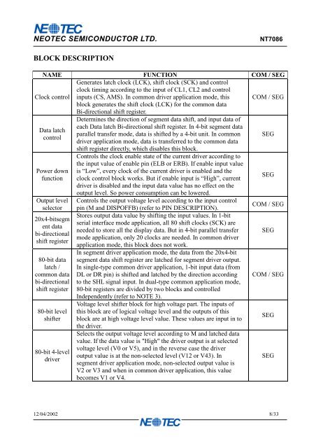
NEOTEC SEMICONDUCTOR LTD.<strong>NT7086</strong>BLOCK DESCRIPTIONNAME FUNCTION COM / SEGClock controlGenerates latch clock (LCK), shift clock (SCK) and controlclock timing according to the input of CL1, CL2 and controlinputs (CS, AMS). In common driver application mode, this COM / SEGblock generates the shift clock (LCK) for the common dataBi-directional shift register.Determines the direction of segment data shift, and input data ofeach Data latch Bi-directional shift register. In 4-bit segment dataData latchparallel transfer mode, data is shifted by a 4-bit unit. In common SEGcontroldriver application mode, data is transferred to the common datashift register directly, which disables this block.Power downfunctionOutput levelselector20x4-bitsegment databi-directionalshift register80-bit datalatch /common databi-directionalshift register80-bit levelshifter80-bit 4-leveldriverControls the clock enable state of the current driver according tothe input value of enable pin (ELB or ERB). If enable input valueis “Low”, every clock of the current driver is enabled and theclock control block works. But if enable input is “High”, currentdriver is disabled and the input data value has no effect on theoutput level. So power consumption can be lowered.Controls the output voltage level according to the input controlpin (M and DISPOFFB) (refer to PIN DESCRIPTION).Stores output data value by shifting the input values. In 1-bitserial interface mode application, all 80 shift clocks (SCK) areneeded to store all the display data. But in 4-bit parallel transfermode application, only 20 clocks are needed. In common driverapplication mode, this block does not work.In segment driver application mode, the data from the 20x4-bitsegment data shift register are latched for segment driver output.In single-type common driver application, 1-bit input data (fromDL or DR pin) is shifted and latched by the direction accordingto the SHL signal input. In dual-type common application mode,80-bit registers are divided by two blocks and controlledIndependently (refer to NOTE 3).Voltage level shifter block for high voltage part. The inputs ofthis block are of logical voltage level and the outputs of thisblock are at high voltage level value. These values are input in tothe driver.Selects the output voltage level according to M and latched datavalue. If the data value is "High" the driver output is at selectedvoltage level (V0 or V5), and in the reverse case the driveroutput value is at the non-selected level (V12 or V43). Insegment driver application mode, non-selected output value isV2 or V3 and when in common driver application, this valuebecomes V1 or V4.SEGCOM / SEGSEGCOM / SEGSEGSEG12/04/2002 8/33