HX8369-A02 - Display Future
HX8369-A02 - Display Future
HX8369-A02 - Display Future

You also want an ePaper? Increase the reach of your titles
YUMPU automatically turns print PDFs into web optimized ePapers that Google loves.
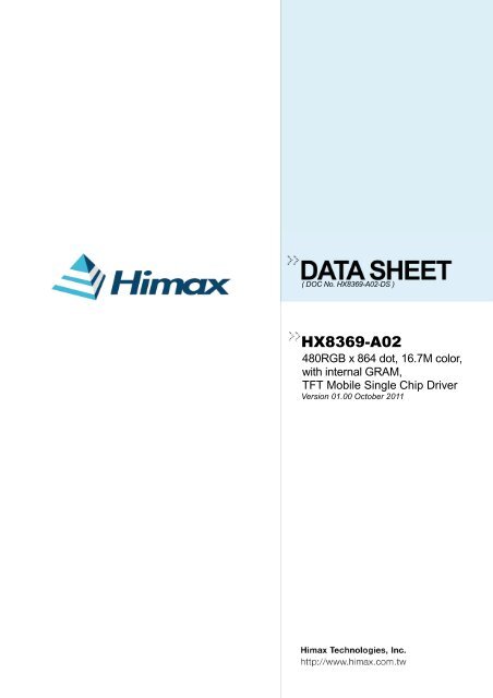
( DOC No. <strong>HX8369</strong>-<strong>A02</strong>-DS )<strong>HX8369</strong>-<strong>A02</strong>480RGB x 864 dot, 16.7M color,with internal GRAM,TFT Mobile Single Chip DriverVersion 01.00 October 2011
<strong>HX8369</strong>-<strong>A02</strong>480RGB x 864 dot, 16.7M color, with internalGRAM, TFT Mobile Single Chip DriverList of Contents1. General Description..........................................................................................................................112. Features .............................................................................................................................................122.1 <strong>Display</strong>........................................................................................................................................122.2 <strong>Display</strong> module...........................................................................................................................122.3 <strong>Display</strong> / Control interface ..........................................................................................................132.4 Input power.................................................................................................................................132.5 Miscellaneous.............................................................................................................................133. Device Overview ...............................................................................................................................143.1 Block diagram.............................................................................................................................143.2 Pin description............................................................................................................................153.3 Pin assignment...........................................................................................................................193.4 PAD coordinates.........................................................................................................................203.4.1 Bump arrangement ................................................................................................................284. Interface .............................................................................................................................................304.1 System interface.........................................................................................................................304.1.1 MIPI DBI-A / DBI-B interface..................................................................................................324.2 Serial data transfer interface (MIPI DBI-C) ................................................................................434.2.2 MIPI DPI interface (<strong>Display</strong> Pixel Interface)...........................................................................474.2.3 DSI system interface..............................................................................................................534.2.4 MDDI Interface (Mobile <strong>Display</strong> Digital Interface)..................................................................674.2.5 Terminology............................................................................................................................684.2.6 Order of data transmission.....................................................................................................694.2.7 Data-STB encoding................................................................................................................695. Function Description ........................................................................................................................825.1 <strong>Display</strong> data GRAM....................................................................................................................825.2 Address counter (AC).................................................................................................................825.3 Source, gate and memory map..................................................................................................835.3.1 480RGB x 864 resolution.......................................................................................................835.3.2 480RGB x 854 resolution.......................................................................................................845.3.3 480RGB x 800 resolution.......................................................................................................855.3.4 480RGB x 640 resolution.......................................................................................................865.3.5 360RGB x 640 resolution.......................................................................................................875.3.6 480RGB x 720 resolution.......................................................................................................885.4 MCU to memory write / read direction........................................................................................895.5 Fully display, partial display, vertical scrolling display ................................................................915.5.1 Fully display ...........................................................................................................................915.5.2 Vertical scrolling display.........................................................................................................975.5.3 Tearing effect output line......................................................................................................1005.6 Color depth conversion ............................................................................................................1045.6.1 Color depth conversion Look-up tables ...............................................................................1045.7 Oscillator...................................................................................................................................1105.8 Source driver ............................................................................................................................ 1115.9 LCD power generation scheme................................................................................................1125.10 DC/DC converter circuit............................................................................................................1135.10.1 Use PFM DC/DC converter .............................................................................................1135.10.2 Use HX5186-A.................................................................................................................1145.11 Idle display ...............................................................................................................................1155.12 Gamma characteristic correction function................................................................................1165.13 Characteristics of I/O................................................................................................................1585.13.1 Output or bi-directional (I/O) pins ....................................................................................158Himax Confidential- P.2-This information contained herein is the exclusive property of Himax and shall not be distributed, reproduced, or disclosedin whole or in part without prior written permission of Himax. October, 2011
<strong>HX8369</strong>-<strong>A02</strong>480RGB x 864 dot, 16.7M color, with internalGRAM, TFT Mobile Single Chip DriverList of Contents October, 20116.2.28 Set_scroll_area (33h) ......................................................................................................2196.2.29 Tearing effect line off (34h) ..............................................................................................2226.2.30 Set_tear_on (35h)............................................................................................................2236.2.31 Set_address_mode (36h) ................................................................................................2246.2.32 Set_scroll_start (37h).......................................................................................................2266.2.33 Idle mode off (38h)...........................................................................................................2276.2.34 Enter_Idle_mode (39h)....................................................................................................2286.2.35 Set_pixel_format (3Ah)....................................................................................................2296.2.36 Write_memory_contiune (3Ch)........................................................................................2306.2.37 Raed_memory_continue (3Eh)........................................................................................2316.2.38 Set tear scan lines (44h)..................................................................................................2326.2.39 Get the current scanline(45h) ..........................................................................................2336.2.40 Write display brightness (51h) .........................................................................................2346.2.41 Read display brightness value (52h) ...............................................................................2356.2.42 Write CTRL display (53h) ................................................................................................2366.2.43 Read CTRL value display (54h) ......................................................................................2376.2.44 Write content adaptive brightness control (55h)..............................................................2386.2.45 Read content adaptive brightness control (56h)..............................................................2396.2.46 Write CABC minimum brightness (5Eh) ..........................................................................2406.2.47 Read CABC minimum brightness (5Fh) ..........................................................................2416.2.48 Read automatic brightness control self-diagnostic result (68h) ......................................2426.2.49 Read_DDB_start (A1h)....................................................................................................2436.2.50 Read_DDB_continue (A8h) .............................................................................................2456.2.51 Read ID1 (DAh) ...............................................................................................................2466.2.52 Read ID2 (DBh) ...............................................................................................................2476.2.53 Read ID3 (DCh) ...............................................................................................................2486.2.54 SETOSC: Set internal oscillator (B0h).............................................................................2496.2.55 SETPOWER: Set power (B1h) ........................................................................................2506.2.56 SETDISP: Set display related register (B2h)...................................................................2596.2.57 SETRGBIF: Set RGB interface related register (B3h).....................................................2626.2.58 SETCYC: Set display waveform cycle (B4h)...................................................................2636.2.59 SETVCOM: Set VCOM voltage (B6h) .............................................................................2666.2.60 SETEXTC: Set extension command (B9h) .....................................................................2696.2.61 SETMIPI: (BAh) ...............................................................................................................2706.2.62 SETOTP: Set OTP (BBh) ................................................................................................2726.2.63 SETDGCLUT: Set DGC LUT (C1h) .................................................................................2736.2.64 SETID: Set ID (C3h) ........................................................................................................2756.2.65 SETCABC: Set CABC Control (C9h)...............................................................................2766.2.66 SETPANEL (CCh)............................................................................................................2786.2.67 SETGIP (D5h)..................................................................................................................2796.2.68 SETGAMMA: Set gamma curve related setting (E0h) ....................................................2866.2.69 SETOTPKEY (E9h) .........................................................................................................2886.2.70 GETHXID (F4h) ...............................................................................................................2896.2.71 SETCNCD/GETCNCD (FDh) ..........................................................................................2906.2.72 SET SPI READ INDEX (FEh)..........................................................................................2916.2.73 GETSPIREAD: Read command data (FFh) ....................................................................2927. Power Supply ..................................................................................................................................2937.1 Power supply setup ..................................................................................................................2937.1.1 Architecture 1 with PFM circuit ............................................................................................2937.1.2 Architecture 2 with HX5186-A..............................................................................................2947.2 Voltage configuration................................................................................................................2958. Electrical Characteristics ...............................................................................................................2968.1 Absolute maximum ratings.......................................................................................................296Himax Confidential- P.4-This information contained herein is the exclusive property of Himax and shall not be distributed, reproduced, or disclosedin whole or in part without prior written permission of Himax. October, 2011
<strong>HX8369</strong>-<strong>A02</strong>480RGB x 864 dot, 16.7M color, with internalGRAM, TFT Mobile Single Chip DriverList of Contents October, 20118.2 ESD protection level.................................................................................................................2968.3 DC characteristics ....................................................................................................................2978.4 AC characteristics ....................................................................................................................2988.4.1 DBI Type A interface characteristics ....................................................................................2988.4.2 DBI Type B interface characteristics ....................................................................................2998.4.3 DBI Type C interface characteristics....................................................................................3008.4.4 DPI interface characteristics ................................................................................................3018.4.5 Reset input timing ................................................................................................................3048.4.6 MDDI electrical characteristics.............................................................................................3058.4.7 DPI Interface Power On/Off Timing......................................................................................3088.4.8 DSI D-PHY electrical characteristics....................................................................................3109. Layout Recommendation ...............................................................................................................31810. Maximum Layout Resistance.........................................................................................................31911. Ordering Information ......................................................................................................................32012. Revision History..............................................................................................................................320Himax Confidential- P.5-This information contained herein is the exclusive property of Himax and shall not be distributed, reproduced, or disclosedin whole or in part without prior written permission of Himax. October, 2011
<strong>HX8369</strong>-<strong>A02</strong>480RGB x 864 dot, 16.7M color, with internalGRAM, TFT Mobile Single Chip DriverList of Figures October, 2011Figure 4.1: DBI-A system interface protocol, write to register or GRAM ...................................32Figure 4.2: DBI-A system interface protocol, read from register or GRAM................................32Figure 4.3: DBI-B system interface protocol, write to register or GRAM ...................................33Figure 4.4: DBI-B system interface protocol, read from register or GRAM................................33Figure 4.5 Example of DBI-B system 18-bit parallel bus interface.............................................34Figure 4.6: Write data for RGB 8-8-8 (16.7M colours) bit Input in 24-bit parallel interface........34Figure 4.7: Example of DBI-A- / DBI-B system 18-bit parallel bus interface..............................35Figure 4.8: Write data for RGB 5-6-5 (65k colours) bit input in 18-bit parallel interface ............35Figure 4.9: Write data for RGB 6-6-6(262k colours) bit input in 18-bit parallel interface ...........35Figure 4.10: Write data for RGB 8-8-8 (16.7M colours) bit input in 18-bit parallel interface......36Figure 4.11: Example of DBI-A- / DBI-B system 16-bit bus interface.........................................37Figure 4.12: Write data for RGB 5-6-5 (65k colours) bit input in 16-bit parallel interface ..........37Figure 4.13: Write data for RGB 6-6-6 (262k colours) bit input in 16-bit parallel interface ........38Figure 4.14: Write data for RGB 8-8-8-bit (16.7M colours) input in 16-bit parallel interface......38Figure 4.15: Example of DBI-A- / DBI-B- system 9-bit bus interface .........................................39Figure 4.16: Write data for RGB 5-6-5(65k colours) bit input in 9-bit parallel interface .............39Figure 4.17: Write data for RGB 6-6-6-bit (262k colours) input in 9-bit parallel interface..........40Figure 4.18: Write data for RGB 8-8-8-bit (16.7 M colours) input in 9-bit parallel interface.......40Figure 4.19: Example of DBI-A- / DBI-B-system 8-bit bus interface ..........................................41Figure 4.20: Write data for RGB 5-6-5 (65k colours) bit input in 8-bit parallel interface ............41Figure 4.21: Write data for RGB 6-6-6-bit (262k colours) input in 8-bit parallel interface..........42Figure 4.22: Write data for RGB 8-8-8-bit (16.7 M colours) input in 8-bit parallel interface.......42Figure 4.23: Serial data stream, write mode ..............................................................................43Figure 4.24: DBI Type C: Serial interface protocol 3-wire/4-wire, write mode ...........................44Figure 4.25: Type C:Serial interface protocol 3-wire/4-wire read mode.....................................45Figure 4.26: <strong>Display</strong> module data transfer recovery ..................................................................46Figure 4.27: PCLK cycle.............................................................................................................47Figure 4.28: General timing diagram..........................................................................................48Figure 4.29: DPI (480RGB x 864) timing diagram .....................................................................48Figure 4.30: 16-bit / pixel 65K colours order on the DPI I/F.......................................................50Figure 4.31: 18-bit / pixel: 262k colours order on the DPI I/F ....................................................51Figure 4.32: 24-bit / pixel color order on the RGB I/F ................................................................52Figure 4.33: DSI transmitter and receiver interface ...................................................................53Figure 4.34: DSI transmitter and receiver interface ...................................................................54Figure 4.35: Multiple HS transmission packets..........................................................................55Figure 4.36: Structure of the short packet..................................................................................55Figure 4.37: Structure of the long packet...................................................................................56Figure 4.38: The format of data ID. ............................................................................................56Figure 4.39: show Short- / Long-packet transmission command sequence ..............................57Figure 4.40: Physical connection of MDDI host and client.........................................................67Figure 4.41: MDDI terminology ..................................................................................................68Figure 4.42: Example of Bi-directional MDDI communication....................................................68Figure 4.43: Transmission bit ordering for each type.................................................................69Figure 4.44: Data-STB encoding................................................................................................70Figure 4.45: Data / STB generation & recovery circuit...............................................................70Figure 4.46: Differential connection between host and client ....................................................71Figure 4.47 MDDI packet structure ............................................................................................72Figure 4.48: MDDI Transceiver / Receiver state in hibernation .................................................79Figure 4.49: Host-initiated link wakeup sequence .....................................................................80Figure 4.50: MDDI operation mode............................................................................................81Figure 5.1: MCU to Memory write / read direction .....................................................................89Figure 5.2: MY, MX, MV setting of 480RGB x 864 dot ..............................................................89Figure 5.3: MY, MX, MV setting of 480RGB x 864 dot ..............................................................89Figure 5.4: Address direction settings........................................................................................90Figure 5.5: 480RGB x 864 resolution.........................................................................................91Himax Confidential- P.6-This information contained herein is the exclusive property of Himax and shall not be distributed, reproduced, or disclosedin whole or in part without prior written permission of Himax. October, 2011
<strong>HX8369</strong>-<strong>A02</strong>480RGB x 864 dot, 16.7M color, with internalGRAM, TFT Mobile Single Chip DriverList of Figures 2October, 2011Figure 5.6: 480RGB x 854 resolution.........................................................................................92Figure 5.7: 480RGB x 800 resolution.........................................................................................93Figure 5.8: 480RGB x 640 resolution.........................................................................................94Figure 5.9: 360RGB x 640 resolution.........................................................................................95Figure 5.10: 480RGB x 720 resolution.......................................................................................96Figure 5.11: Vertical scrolling .....................................................................................................97Figure 5.12: Memory map of vertical scrolling 1 ........................................................................97Figure 5.13: Memory map of vertical scrolling 2 ........................................................................98Figure 5.14: Vertical scroll example 1 ........................................................................................99Figure 5.15: Vertical scroll example 2 ........................................................................................99Figure 5.16: Tearing effect output line–mode 1........................................................................100Figure 5.17: Tearing effect output line–mode 2........................................................................100Figure 5.18: Tearing effect output line–timing diagrm ..............................................................100Figure 5.19: Tearing effect output line –tearing effect line timing.............................................101Figure 5.20: Tearing effect output line–definition of tf, tr ..........................................................101Figure 5.21: Tearing effect output line–example 1 (Timing) .....................................................102Figure 5.22: Tearing effect output line–example 1 (Image)......................................................102Figure 5.23: Tearing effect output line–example 2 (Timing) .....................................................103Figure 5.24: Tearing effect output line–example 2 (Image)......................................................103Figure 5.25: OSC aritecture .....................................................................................................110Figure 5.26: LCD power generation scheme ...........................................................................112Figure 5.27: DC/DC converter circuit (PFM Type C)–PCCS=10..............................................113Figure 5.28: DC/DC converter circuit (HX5186-A) ...................................................................114Figure 5.29: Idle mode grayscale control .................................................................................115Figure 5.30: Grayscale control .................................................................................................116Figure 5.31: Gamma resister stream and gamma reference voltage ......................................118Figure 5.32: Gamma resister stream .......................................................................................119Figure 5.33: Sleep out flow chart–command and self-diagnostic functions.............................160Figure 5.34: Sleep out flow chart internal function detection ...................................................161Figure 5.35: Case 1: RESX line is held high or unstable by host at power on ........................163Figure 5.36: Case 2: RESX line is held low by host at power on.............................................164Figure 5.37: CABC block diagram............................................................................................165Figure 5.38: Module architecture .............................................................................................166Figure 5.39: CABC gain / CABC duty generation ....................................................................167Figure 5.40: CABC_PWM_OUT output duty............................................................................168Figure 5.41: OTP programming sequence...............................................................................173Figure 5.42: OTP programming sequence example 1. ............................................................175Figure 5.43: OTP programming sequence example 2. ............................................................176Figure 5.44: OTP programming sequence index 0x1Bh read flow. .........................................177Figure 5.45: OTP programming sequence read flow. ..............................................................178Figure 7.1: Power supply with PFM circuit ...............................................................................293Figure 7.2: Power supply with HX5186-A ................................................................................294Figure 8.1: DBI Type A interface characteristics(CLK-E mode) ...............................................298Figure 8.2: DBI Type B interface characteristics ......................................................................299Figure 8.3: DBI Type C interface characteristics......................................................................300Figure 8.4: DPI interface characteristics ..................................................................................301Figure 8.5: Vertical Timings for RGB I/F...................................................................................302Figure 8.6: Horizontal Timing for RGB I/F ................................................................................303Figure 8.7: Reset input timing ..................................................................................................304Figure 8.8 Power On Timing ....................................................................................................308Figure 8.9 Power Off Timing ....................................................................................................309Figure 8.10: Electrical functions of a fully D-PHY transceiver..................................................310Figure 8.11: Shows both the HS and LP signal levels .............................................................310Figure 8.12: Input Glitch Rejections of Low-Power Receivers.................................................313Figure 8.13: DDR Clock Definition ...........................................................................................315Himax Confidential- P.7-This information contained herein is the exclusive property of Himax and shall not be distributed, reproduced, or disclosedin whole or in part without prior written permission of Himax. October, 2011
<strong>HX8369</strong>-<strong>A02</strong>480RGB x 864 dot, 16.7M color, with internalGRAM, TFT Mobile Single Chip DriverList of Figures October, 2011Figure 8.14: Data to Clock Timing Definitions..........................................................................316Figure 9.1: Layout recommendation ........................................................................................318Himax Confidential- P.8-This information contained herein is the exclusive property of Himax and shall not be distributed, reproduced, or disclosedin whole or in part without prior written permission of Himax. October, 2011
<strong>HX8369</strong>-<strong>A02</strong>480RGB x 864 dot, 16.7M color, with internalGRAM, TFT Mobile Single Chip DriverList of Tables October, 2011Table 4.1: Interface selection .....................................................................................................30Table 4.2: Pin connection based on different interface ..............................................................31Table 4.3: Data types for processor-sourced packets................................................................58Table 4.4: Shows the error report bit definitions.........................................................................65Table 4.5: The complete set of peripheral-to-processor data types...........................................66Table 4.6: List of supported MDDI packet ..................................................................................73Table 4.7: Operation mode list ...................................................................................................81Table 5.1: Addresses counter range...........................................................................................82Table 5.2: Memory map of 480RGB x 864 resolution ................................................................83Table 5.3: Memory map of 480RGB x 854 resolution ................................................................84Table 5.4: Memory map of 480RGB x 800 resolution ................................................................85Table 5.5: Memory map of 480RGB x 640 resolution ................................................................86Table 5.6: Memory map of 360RGB x640 resolution .................................................................87Table 5.7: Memory map of 480RGB x 720 resolution ................................................................88Table 5.8: 480RGB x 864 resolution (SRAM assignment) .........................................................91Table 5.9: 480RGB x 854 resolution (SRAM assignment) .........................................................92Table 5.10: 480RGB x 800 resolution (SRAM assignment) .......................................................93Table 5.11: 480RGB x 640 resolution (SRAM assignment) .......................................................94Table 5.12: 360RGB x 640 resolution (SRAM assignment) .......................................................95Table 5.13: 480RGB x 720 resolution (SRAM assignment) .......................................................96Table 5.14: AC characteristics of tearing effect signal .............................................................101Table 5.15: Look-up tables-1....................................................................................................104Table 5.16: Look-up tables-2....................................................................................................105Table 5.17: Look-up tables-3....................................................................................................106Table 5.18: Look-up tables-4....................................................................................................107Table 5.19: Look-up tables-5....................................................................................................108Table 5.20: Look-up tables-6....................................................................................................109Table 5.21: Gamma-Adjustment registers................................................................................117Table 5.22: Offset adjustment 0~5 ...........................................................................................120Table 5.23: Center adjustment .................................................................................................120Table 5.24: VinP0 .....................................................................................................................121Table 5.25: VinP1 .....................................................................................................................122Table 5.26: VinP2 .....................................................................................................................123Table 5.27: VinP14 ...................................................................................................................124Table 5.28: VinP15 ...................................................................................................................125Table 5.29: VinP16 ...................................................................................................................126Table 5.30: VinP5 .....................................................................................................................128Table 5.31: VinP11 ...................................................................................................................130Table 5.32: VinP3 .....................................................................................................................131Table 5.33: VinP4 .....................................................................................................................132Table 5.34: VinP6 .....................................................................................................................132Table 5.35: VinP7 .....................................................................................................................133Table 5.36: VinP8 .....................................................................................................................133Table 5.37: VinP9 .....................................................................................................................134Table 5.38: VinP10 ...................................................................................................................134Table 5.39: VinP12 ...................................................................................................................135Table 5.40: VinP13 ...................................................................................................................135Table 5.41: VinN0 .....................................................................................................................136Table 5.42: VinN1 .....................................................................................................................137Table 5.43: VinN2 .....................................................................................................................138Table 5.44: VinN14 ...................................................................................................................139Table 5.45: VinN15 ...................................................................................................................140Table 5.46: VinN16 ...................................................................................................................141Table 5.47: VinN5 .....................................................................................................................143Table 5.48: VinN11 ...................................................................................................................145Himax Confidential- P.9-This information contained herein is the exclusive property of Himax and shall not be distributed, reproduced, or disclosedin whole or in part without prior written permission of Himax. October, 2011
Table 5.49: VinN3 .....................................................................................................................146Table 5.50: VinN4 .....................................................................................................................147Table 5.51: VinN6 .....................................................................................................................147Table 5.52: VinN7 .....................................................................................................................148Table 5.53: VinN8 .....................................................................................................................148Table 5.54: VinN9 .....................................................................................................................149Table 5.55: VinN10 ...................................................................................................................149Table 5.56: VinN12 ...................................................................................................................150Table 5.57: VinN13 ...................................................................................................................150Table 5.58: Voltage calculation formula of 64-grayscale voltage (positive polarity).................152Table 5.59: Voltage calculation formula of 64-grayscale voltage (negative polarity) ...............154Table 5.60: Voltage calculation formula of 256-grayscale voltage (positive/negative polarity)157Table 5.61 Characteristics of output or bi-directional (I/O) pins ...............................................158Table 5.62 Characteristics of input pins ...................................................................................158Table 5.63 CABC timing table ..................................................................................................168Table 5.64: OTP Programming sequence ................................................................................174Table 7.1: Adoptability of component .......................................................................................295Table 8.1: Absolute maximum rating ........................................................................................296Table 8.2: ESD protection level ................................................................................................296Table 8.3: DC characteristic .....................................................................................................297Table 8.4: DBI Type A interface characteristics ........................................................................298Table 8.5: DBI Type B interface characteristics........................................................................299Table 8.6: DBI Type C interface characteristics .......................................................................300Table 8.7: DPI interface characteristics....................................................................................301Table 8.8 Vertical Timings for RGB I/F .....................................................................................302Table 8.9 Horizontal Timings for RGB I/F.................................................................................303Table 8.10: Reset timing...........................................................................................................304Table 8.11: LP Transmitter DC Specifications ..........................................................................311Table 8.12: LP Transmitter AC Specifications..........................................................................311Table 8.13: HS Receiver DC Specifications .............................................................................312Table 8.14: HS Receiver AC Specifications .............................................................................312Table 8.15: LP Receiver DC Specifications..............................................................................313Table 8.16: LP Receiver AC Specifications..............................................................................313Table 8.17: Contention Detector DC Specifications .................................................................314Table 8.18: HS Data Transmission Timing Parameters ...........................................................315Table 8.19: Data to Clock Timing Specifications......................................................................317Table 10.1: Maximum layout resistance ...................................................................................319Himax Confidential- P.10-This information contained herein is the exclusive property of Himax and shall not be distributed, reproduced, or disclosedin whole or in part without prior written permission of Himax. October, 2011
<strong>HX8369</strong>-<strong>A02</strong>480RGB x 864 dot, 16.7M color, with internalGRAM, TFT Mobile Single Chip DriverVersion 01 October, 20111. General DescriptionThis document describes Himax’s <strong>HX8369</strong>-<strong>A02</strong> supports WVGA resolution drivingcontroller. The <strong>HX8369</strong>-<strong>A02</strong> is designed to provide a single-chip solution thatcombines a source driver, power supply circuit to drive a TFT dot matrix LCD with480RGBx864 dots at maximum.The <strong>HX8369</strong>-<strong>A02</strong> can be operated in low-voltage condition for the interface andintegrated internal boosters that produce the liquid crystal voltage, breeder resistanceand the voltage follower circuit for liquid crystal driver. In addition, The <strong>HX8369</strong>-<strong>A02</strong>also supports various functions to reduce the power consumption of a LCD systemvia software control.The <strong>HX8369</strong>-<strong>A02</strong> supports several interface modes, including MPU MIPI DBI TypeA/Type B interface mode, MIPI DPI/DBI Type C interface mode, MIPI DSI (<strong>Display</strong>Serial Interface) interface mode and MDDI (Mobile <strong>Display</strong> Digital Interface) interfacemode. The interface mode is selected by the external hardware pins BS3~0.The <strong>HX8369</strong>-<strong>A02</strong> is suitable for any small portable battery-driven and long-termdriving products, such as small PDAs, digital cellular phones and bi-directionalpagers.Himax Confidential-P.11-This information contained herein is the exclusive property of Himax and shall not be distributed, reproduced, or disclosedin whole or in part without prior written permission of Himax. October, 2011
<strong>HX8369</strong>-<strong>A02</strong>480RGBx864dots, TFT Mobile Single Chip Driver2. FeaturesDATA SHEET V012.1 <strong>Display</strong> Single chip solution for a WVGA GIP (Gate In Panel) type TFT LCD display Resolution: 480RGB x 864 480RGB x 854 480RGB x 800 480RGB x 640 480RGB x 720 360RGB x 640 <strong>Display</strong> color modes Full color mode: 16.7M colours (24-bit 8(R):8(G):8(B)) Reduce color mode: 262k colours (18-bit 6(R):6(G):6(B)) 65k colours (16-bit 5(R):6(G):5(B)) 8 colors (Idle mode on): 8 colors (3-bit binary mode)2.2 <strong>Display</strong> module Support 1440 source channel outputs Internal level shifter for GIP gate control Supports 1-dot / 2-dot / column / Zig-Zag inversion Gamma correction (1 preset gamma curve) On module VCOM control (-2 to 0V common electrode output voltage range) On module DC/DC converter VSP=4.7 to 5.7V VSN=-5.7 to -4.7V Positive source output voltage level: VSPR=3.5V to 5V Negative source output voltage level: VSNR=-5V to -3.5V Positive gate driver output voltage level: VGH=+9V to +20V Negative gate driver output voltage level: VGL=-6V to -13.5V GIP most negative reference voltage: LVGL=VGL –VDD3 VCOM=-2.0V to 0V, a step=16mV Frame memory area 480 (H) x 864 (V) x 24-bitHimax Confidential-P.12-This information contained herein is the exclusive property of Himax and shall not be distributed, reproduced, or disclosedin whole or in part without prior written permission of Himax. October, 2011
<strong>HX8369</strong>-<strong>A02</strong>480RGBx864dots, TFT Mobile Single Chip Driver2.3 <strong>Display</strong> / Control interfaceDATA SHEET V01 <strong>Display</strong> interface types supported MPU mode MIPI-DBI Type B (80 System) interface (16- / 18- / 24-bit bus) MIPI-DBI Type A (68 System) interface (16- / 18- bit bus) MIPI-DBI Type C (Serial data transfer interface) interface MIPI-DSI (<strong>Display</strong> Serial Interface) interface Support DSI Version 1.01 Support D-PHY version 0.90 MDDI (Mobile <strong>Display</strong> Digital Interface) interface Support VESA Mobile <strong>Display</strong> Digital Interface Standard Version 1.2 RGB mode 16 bit/pixel R(5), G(6), B(5) 18 bit/pixel R(6), G(6), B(6) 24 bit/pixel R(8), G(8), B(8)2.4 Input power I/O and interface power supply (VDD1): 1.65V to 3.3V Analog power supply (VDD2): 2.3V to 4.8V Logic power supply (VDD3): 2.3V to 4.8V DSI power supply (DSI_VCC): 1.65V to 3.3V MDDI power supply (DSI_VCC): 2.3V to 3.3V OTP programming voltage (VPP): 7.5V ± 0.2V2.5 Miscellaneous Partial display mode Software programmable color depth mode Oscillator for display clock generation Low power consumption, suitable for battery operated systems CMOS compatible inputs Proprietary multi phase driving for lower power consumption GAS function for preventing image sticking when abnormal power off Optimized layout for COG assembly Temperature range: -40 to +85 °C HBM ESD (Human Body Mode)>2KV, MM(Machine Mode)>±200V andLatch up>±200mA Support inversion mode DC/DC converter for source Support DC COM driving VCOM voltage generator On-chip OTP program voltage generator OTP memory to store initialization register settings 3 times MTP for VCOM setting ,ID setting Support CABC (Content Adaptive Brightness Control) function Support DGC (Digital Gamma Correction) functionHimax ConfidentialThis information contained herein is the exclusive property of Himax and shall not be distributed, reproduced, or disclosed-P.13-in whole or in part without prior written permission of Himax.October, 2011
<strong>HX8369</strong>-<strong>A02</strong>480RGBx864dots, TFT Mobile Single Chip Driver3. Device OverviewDATA SHEET V013.1 Block diagramNote:MPU I/F display data pathRGB I/F display data pathPWM_OUTS1 ~ S1441VPPBS3-0CSXRDX_EWRX_DCXDCX_SCLDB23~0SDISDOVSYNC_TEHSYNCPCLKDERESXDSI_LDO_ENB/MDDI_LDO_ENBDSI_CLKP(MDDI_STBP) /DSI_CLKN(MDDI_STBN)DSI_D0P(MDDI_D0P)/DSI_D0N(MDDI_D0N)DSI_D1P(MDDI_D1P)/DSI_D1N(MDDI_D1N)DSI_VCC /MDDI_VCCDSI_VSS/MDDI_VSSOSCTEST2~1424222OTPMPU I/F24-bit18-bit16-bit9-bit8-bitSPI I/F3-wireRGB I/F16-bit18-bit24-bitDSI / MDDIInterfaceRC OSC24-bitdisplaydata24-bitdisplaydataGeneratorTimingInternalregisterGRAMcontrolGRAMModeselectionABC functionDigitalGammaCorrectionCABC functionTimingControlSourcedriverD/A ConvertercircuitData LatchGrayscale voltagegeneratorGamma adjusting circuitGateControlUnitV0~255220VGSVTESTOUTP /VTESTOUTNTEGOUTL_1~GOUTL_10GOUTR1~GOUTR_10VCIVSSAPFMDC / DC ConverterVCOM CricuitVoltage referenceVSSACVSSDVCSW1VCSW2VSPVSNC21AP / C21ANC22AP / C22ANC23AP / C23ANC24AP / C24ANV GHV GLC41AP / C41ANLVGLVCOMRV COMVSPRVSNRVREFVDDDVDDDNDSI_LDOHimax ConfidentialThis information contained herein is the exclusive property of Himax and shall not be distributed, reproduced, or disclosed-P.14-in whole or in part without prior written permission of Himax.October, 2011
<strong>HX8369</strong>-<strong>A02</strong>480RGBx864dots, TFT Mobile Single Chip Driver3.2 Pin descriptionDATA SHEET V01Host interface pinsSignals I/O Pin no. ConnectedwithBS3 ~ BS0 I 4VSSD /VDD1CSX I 1 MPURESX I 1MPU orreset circuitRDX_E I 1 MPUDCX_SCL I 1 MPUDescriptionSelect the MPU interface mode as listed below:BS3 BS2 BS1 BS0 MPU interface mode DB pins<strong>Display</strong>mode0 0 0 0DBI TYPE-A 8-bit DB23-DB8: Unused,(CLK-E)DB7-DB0: DataType 10 0 0 1DBI TYPE-A 9-bit DB23-DB9:Unused,(CLK-E)DB8-DB0: DataType 10 0 1 0DBI TYPE-A 16-bit DB23-DB16: Unused,(CLK-E)DB15-DB0: DataType 10 0 1 1DBI TYPE-A 18-bit DB23-DB18: Unused,(CLK-E)DB17-DB0: DataType 10 1 0 0 DBI TYPE-B 8-bitDB23-DB8: UnusedDB7-DB0: DataType 10 1 0 1 DBI TYPE-B 9-bitDB23-DB9:Unused,DB8-DB0: DataType 10 1 1 0 DBI TYPE-B 16-bitDB23-DB16: Unused,DB15-DB0: DataType 10 1 1 1 DBI TYPE-B 18-bitDB23-DB18: Unused,DB17-DB0: DataType 1DSI_CLKP,1 0 0 0DSI_CLKN,DSIDSI_D0P,(Command mode)DSI_D0N,Type 1DSI_D1P, DSI_D1N1 0 0 1MDDI _STBP,MDDI _STBN,3-wire serial + MDDIMDDI _D0P,interface + external R(note 1)MDDI _D0N,MDDI _D1P,-MDDI _D1N,1 0 1 0 DBI TYPE-B 24-bit DB23-DB0: Data Type 1MDDI _STBP,1 0 1 1MDDI _STBN,3-wire serial + MDDIMDDI _D0P,interface + internal R(note 1)MDDI _D0N,MDDI _D1P,-MDDI _D1N,DSI_CLKP,DSI_CLKN,1 1 0 0 DSI (Video mode) DSI_D0P,Type 3DSI_D0N,DSI_D1P, DSI_D1N1 1 0 1DPI/DBI TYPE-C SDI/SDO,Option 1DB23-DB0Type 31 1 1 0DPI/DBI TYPE-C SDI/SDO,Option 2DB23-DB0Type 31 1 1 1DPI/DBI TYPE-C SDI/SDO,Option 3DB23-DB0Type 3Pixel format (RGB565 / RGB666 / RGB888) is selected by DCS command (0x3Ah)Note 1: 3-wire serial Interface only active on MDDI / Hibernation mode(1-lane only).Must be connected to VSSD or VDD1.Chip select signal.Low: chip can be accessed;High: chip cannot be accessed.If this pin is not used, please connect it to VSSD or VDD1.Reset pin. Setting either pin low initializes the LSI. Must be reset afterpower is supplied (Must be connected to VSSD or VDD1).DBI Type-A: 0: Read/Write disable, 1: Read / Write enable.DBI Type-B: Serves as a read signal and read data at the low level.If not use, let it open or connected to VDD1.DBI Type-A/B: Data / Command Selection pinDBI Type-C: it servers as SCL (Serial Clock)If not use, let it open or connected to VDD1.Himax Confidential-P.15-This information contained herein is the exclusive property of Himax and shall not be distributed, reproduced, or disclosedin whole or in part without prior written permission of Himax. October, 2011
<strong>HX8369</strong>-<strong>A02</strong>480RGBx864dots, TFT Mobile Single Chip DriverDATA SHEET V01Power supply pinsPCCS0 ~ PCCS1 I 2VDD1 I 5VDD2 I 6VSSD /VDD3PowersupplyPowersupplySelect the VSP/VSN bumping method as listed below:PCCS1 PCCS0 Driving mode0 0 Setting invalid0 1 Setting invalid1 0 PFM one Inductor Mode (Type C)1 1 Charge Bump Mode(Use HX5186-A)Must be connected to VSSD or VDD3.A power supply for the I/O circuit. VDD1=1.65 to 3.3VA power supply for the analog power. VDD2=2.3 to 4.8VVDD2 input level should be same as VDD3 input level to avoid thelevel-mismatching at internal level shifter circuit.VDD3 I 6PowersupplyA power supply for the logic power, DC/DC converter VDD3=2.3 to 4.8V.VSSA P 6Power Analoge ground. VSSA=0V. When using the COG method, connect tosupply VSSD on the FPC to prevent noise.VSSAC P 2PowersupplyAnaloge ground. Must connect to VSSA on the FPC.VSSD P 16Power Ground for the internal logic. VSSD=0V. When using the COG method,supply connect to VSSA on the FPC to prevent noise.VPP I 2Power External high voltage pin used in OTP mode and operates at 7.5V.supply If not used, let it open.Output Pins of Power and reference voltageVSP I 7Stabilizing Input voltage from the set-up circuit (4.7V to 5.5V). it is generated fromcapacitor VDD3.VSN I 6Stabilizing Input voltage from the set-up circuit (-4.7V to -5.5V). it is generatedcapacitor from VDD3.VSPC I 1 VSP Positive boosting reference voltage input.VSNC I 1 VSN Negative boosting reference voltage input.VSPR O 2StabilizingcapacitorPositive regulated voltage output (3.5V to VSP - 0.5)VSNR O 2StabilizingcapacitorPositive regulated voltage output (-3.5V to VSN + 0.5)VDDD O 19StabilizingcapacitorInternal logic voltage outputVDDDN O 5StabilizingcapacitorInternal logic voltage output (-2.5V fixed)VREF O 2Stabilizing Reference voltage from internal band gap circuit. The tolerance ofcapacitor VREF voltage is ± 3 %.(1.8V fixed)VGH O 10Stabilizing Output voltage from the step-up circuit, it is generated from VSP andcapacitor VSN. Connect to a stabilizing capacitor between VSSA and VGH.VGL O 10Output voltage from the step-up circuit, it is generated from VSP andStabilizingVSN. Connect to a stabilizing capacitor between VSSA and VGL. Placecapacitora schottkey barrier diode between VSSA and VGL.LVGL O 15VCOM O 14StabilizingcapacitorStabilizingcapacitorMost negative voltage for some special GIP circuits. If not used,connect to VGL.The power supply of common voltage in DC com driving. The voltagerange is set between -2V to 0V. It must be connected a stabilizingcapacitor 2.2u to VSSD.VCOMR I 1 Input The input pad of external VCOM voltage.DC/DC pumpingC21AP, C21ANC22AP, C22ANC23AP, C23ANC24AP, C24ANI/O 16I/O 16C41AP, C41AN I/O 6Step-upCapacitorStep-upCapacitorStep-upCapacitorVCSW1 O 4 -VCSW2 O 4 -Connect to the step-up capacitors according to the DC/DC pumpingfactor by pumping the VGL voltage.Connect to the step-up capacitors according to the DC/DC pumpingfactor by pumping the VGH voltage.Connect to the step-up capacitors according to the DC/DC pumpingfactor by pumping the LVGL voltage.Boosting control output1, it needs to connect to the gate pin of NMOSon external DC/DC converter circuit. (0 to VDD3)Boosting control output2, it needs to connect to the gate pin of PMOSon external DC/DC converter circuit. (0 to VDD3)Himax ConfidentialThis information contained herein is the exclusive property of Himax and shall not be distributed, reproduced, or disclosed-P.17-in whole or in part without prior written permission of Himax.October, 2011
<strong>HX8369</strong>-<strong>A02</strong>480RGBx864dots, TFT Mobile Single Chip DriverCABC & ABC & Ambient light sensorCABC_PWM_OUT O 1 -Test PinsOSC I 1 OpenTEST1 I 1 OpenTEST2 I 1 OpenVTESTOUTP O 1 OpenVTESTOUTN O 1 OpenDUMMYR1DUMMYR2- 2 OpenDATA SHEET V01Backlight on/fff control pin. If use CABC function, the pin can connectto external LED driver IC. The output voltage range=0 to VDD1.Oscillator input for test purpose.If not used, please let it open or connected to VSSD.(weak pull low)A test pin. This pin is by internal logic function test.This pin can outputon FPC. If not used, let it open or connected to VSSD.(weak pull low)A test pin. This pin is by internal logic function test.This pin can outputon FPC. If not used, let it open or connected to VSSD.(weak pull low)A test pin. Disconnect it. This pin will output Gamma voltage. This pincan output on FPC.A test pin. Disconnect it. This pin will output Gamma voltage. This pincan output on FPC.Dummy pads. Available for measuring the COG contact resistance.They are short-circuited within the chip.DUMMY17~1 - 17 Open Not used. Let it open.IOGNDDUM - 3 Open Dummy pad. Connect to grand internally.MIPI-DSI interface partsDSI_D0P,MIPI-DSI Data differential signal input pins. (Data lane 0)I/O 6 DSI HostDSI_D0NIf not used, please let it connected to VSSD.DSI_CP,MIPI-DSI CLOCK differential signal input pins.I 6 DSI HostDSI_CNIf not used, please let it connected to VSSD.DSI_D1P,MIPI-DSI Data differential signal input pins. (Data lane 1)I 6 DSI HostDSI_D1NIf not used, please let it connected to VSSD.DSI_VCC P 5 Power Supply Power supply for the MIPI DSI analog power.DSI_VCC=1.65V to 3.3VDSI_VSS P 9 GroundMIPI DSI analogy ground. DSI_VSS=0V. When using the COG method,connect to VSSA on the FPC to prevent noise.DSI_LDO O 2 CapacitorDSI:DSI regulator output pin. (1.2V to 1.3V)Connect to a stabilizing capacitor between DSI_VSS and DSI_LDOIf not used, please open these pins.DSI_LDO_ENB I 1 InputDSI I/F:Control signal of DSI_LDO. The default setting of DSI_LDO_ENB isLow.High: Disable the DSI_LDO.Low: Enable the DSI_LDO.It must be connected to VDD1 or VSSD. (latch type)MDDI interface partsMDDI_STBP,MDDI _STBNMDDI _D0P,MDDI _D0NMDDI _D1P,MDDI _D1N- 6- 6- 6High SpeedInterfaceHostHigh SpeedInterfaceHostHigh SpeedInterfaceHostHigh Speed Interface clock differential signal input pins.When BS[3:0]=1001(MDDI interface + external R), please connect toa terminal resistance (100Ω) between MDDI_STBP and MDDI_STBN.If not used, please let it connected to VSSD.High Speed Interface Data differential signal input pins (Data lane 0).When BS[3:0]=1001(MDDI interface + external R), please connect toa terminal resistance (100Ω) between MDDI_D0P and MDDI_D0N.If not used, please let it connected to VSSD.High Speed Interface Data differential signal input pins. (Data lane 1)When BS[3:0]=1001(MDDI interface + external R), please connect toa terminal resistance (100Ω) between MDDI_D1P and MDDI_D1N.If not used, please let it connected to VSSD.MDDI _VCC P 5Power Supplyor CapacitorHigh Speed Interface I/O power supply pin, 2.3V to 3.3V.MDDI _VSS P 9 Ground High Speed Interface I/O ground pin.MDDI _LDO O 2 CapacitorHigh Speed Interface regulator output pin.Connect to a stabilizing capacitor between MDDI_VSS andMDDI_LDO.If not used, please open these pins.MDDI_LDO_ENB I 1 InputMDDI I/F:Control signal of MDDI_LDO. The default setting of MDDI_LDO_ENBis Low.High: Disable the MDDI _LDO.Low: Enable the MDDI _LDO.It must be connected to VDD1 or VSSD. (latch type)Himax ConfidentialThis information contained herein is the exclusive property of Himax and shall not be distributed, reproduced, or disclosed-P.18-in whole or in part without prior written permission of Himax.October, 2011
<strong>HX8369</strong>-<strong>A02</strong>480RGBx864dots, TFT Mobile Single Chip Driver3.3 Pin assignmentDATA SHEET V01(A1)Chip Size : 22430 x 1701 um(Include scribe line = 80 um)Chip thickness: 250 um ± 25 umPad Location: PAD CenterCoordinate Origin: Chip CenterAu Bump Size:1. 50 um x 80 umInput:No.1 ~ No.3122. 15 um x 95 umStaggered LCD output sideNo.313 ~ No.1760The chip size includes the core sizeseal ring size, and scribe line sizeAu bump pitch: Refer to Pad Coordinate .Au bump height : 12 um ± 3 umNumbers in the figure corresponds topad coordinate numbers .ChipTop ViewBUMPNO.1DUMMY1CGOUT1_LCGOUT2_LCGOUT3_LCGOUT4_LCGOUT5_LCGOUT5_LCGOUT6_LCGOUT6_LCGOUT7_LCGOUT7_LCGOUT8_LCGOUT8_LCGOUT9_LCGOUT10_LVGLVGLVGLVBIASLVGLLVGLLVGLDUMMY2VCOMVCOMVCOMDUMMY3DUMMYR1DUMMYR2DUMMY4VGLVGLVGLLVGLLVGLLVGLLVGLLVGLVCOMVCOMVCOMVCOMC41APC41APC41APC41ANC41ANC41ANVGHVGHVGHVGHVGHVGHC21APC21APC21APC21APC21ANC21ANC21ANC21ANC23APC23APC23APC23APC23ANC23ANC23ANC23ANC22APC22APC22APC22APC22ANC22ANC22ANC22ANC24APC24APC24APC24APC24ANC24ANC24ANC24ANVPPVPPVDDDNVDDDNVDDDNVDDDNVDDDNVDD2VDD2VDD2VDD2VDD2VDD2VREFVREFVSSAVSSAVSSAVSSAVSSAVSSAVSSDVSSDVSSDVSSDVSSDVSSDVSSDVSSDVDDDVDDDVDDDVDDDVDDDVDDDVDD1VDD1VDD1VDD1VDD1CABC_PWM_OUTTETEST1TEST2BS0BS1BS2BS3RESXIOGNDDUMDB23/TS7DB22/TS6DB21/TS5DB20/TS4DB19/TS3DB18/TS2DB17/TS1DB16/TS0DB15DB14DB13DB12DB11DB10DB9DB8DB7DB6DB5DB4DB3DB2DB1DB0IOGNDDUMRDX_EWRX_DCXDCX_SCLCSXIOGNDDUMSDISDOVSYNCHSYNCDEPCLKDSI_LDO_ENB/MDDI_LDO_ENBDUMMY5OSCPCCS0PCCS1DSI_VSS/MDDI_VSSDSI_D1P/MDDI_D1PDSI_D1P/MDDI_D1PDSI_D1P/MDDI_D1PDSI_D1N/MDDI_D1NDSI_D1N/MDDI_D1NDSI_D1N/MDDI_D1NDSI_VSS/MDDI_VSSDSI_CP/MDDI_STBPDSI_CP/MDDI_STBPDSI_CP/MDDI_STBPDSI_CN/MDDI_STBNDSI_CN/MDDI_STBNDSI_CN/MDDI_STBNDSI_VSS/MDDI_VSSDSI_D0P/MDDI_D0PDSI_D0P/MDDI_D0PDSI_D0P/MDDI_D0PDSI_D0N/MDDI_D0NDSI_D0N/MDDI_D0NDSI_D0N/MDDI_D0NDSI_VSS/MDDI_VSSDSI_LDO/MDDI_LDODSI_LDO/MDDI_LDODSI_VCC/MDDI_VCCDSI_VCC/MDDI_VCCDSI_VCC/MDDI_VCCDSI_VCC/MDDI_VCCDSI_VCC/MDDI_VCCDSI_VSS/MDDI_VSSDSI_VSS/MDDI_VSSDSI_VSS/MDDI_VSSDSI_VSS/MDDI_VSSDSI_VSS/MDDI_VSSVSSACVSSACVSSDVSSDVSSDVSSDVSSDVSSDVSSDVSSDVDDDVDDDVDDDVDDDVDDDVDDDVDDDVDDDVDDDVDDDVDDDVDDDVDDDVSPRVSPRVSPCVSPVSPVSPVSPVSPVSPVSPVCSW1VCSW1VCSW1VCSW1VCSW2VCSW2VCSW2VCSW2VSNRVSNRVSNCVSNVSNVSNVSNVSNVSNVDD3VDD3VDD3VDD3VDD3VDD3VGHVGHVGHVGHVCOMVCOMVCOMVCOMLVGLLVGLLVGLLVGLVTESTOUTPDUMMY6VCOMRVTESTOUTNVCOMVCOMVCOMDUMMY7DUMMY8LVGLLVGLLVGLVBIASVGLVGLVGLVGLCGOUT10_RCGOUT9_RCGOUT8_RCGOUT8_RCGOUT7_RCGOUT7_RCGOUT6_RCGOUT6_RCGOUT5_RCGOUT5_RCGOUT4_RCGOUT3_RCGOUT2_RNO.312CGOUT1_RDUMMY9DUMMY10Face Up(Bump View)<strong>HX8369</strong>-<strong>A02</strong> PinAssignmentXYDUMMY17S1441S1440S1439S1438S722S721DUMMY14DUMMY13DUMMY12DUMMY11S720S719NO.1760NO.1033S2S2S1DUMMY16DUMMY15NO.313(A2)Himax ConfidentialThis information contained herein is the exclusive property of Himax and shall not be distributed, reproduced, or disclosed-P.19-in whole or in part without prior written permission of Himax.October, 2011
<strong>HX8369</strong>-<strong>A02</strong>480RGBx864dots, TFT Mobile Single Chip Driver3.4 PAD coordinatesDATA SHEET V01No. Name X Y No. Name X Y No. Name X Y No. Name X Y1 DUMMY1 -10885 -672 61 C21AN -6685 -672 121 VDDD -2485 -672 181DSI_D1P /MDDI_D1P1715 -6722 CGOUT1_L -10815 -672 62 C21AN -6615 -672 122 VDD1 -2415 -672 182DSI_D1N /MDDI_D1N1785 -6723 CGOUT2_L -10745 -672 63 C23AP -6545 -672 123 VDD1 -2345 -672 183DSI_D1N /MDDI_D1N1855 -6724 CGOUT3_L -10675 -672 64 C23AP -6475 -672 124 VDD1 -2275 -672 184DSI_D1N /MDDI_D1N1925 -6725 CGOUT4_L -10605 -672 65 C23AP -6405 -672 125 VDD1 -2205 -672 185DSI_VSS /MDDI_VSS1995 -6726 CGOUT5_L -10535 -672 66 C23AP -6335 -672 126 VDD1 -2135 -672 186DSI_CP /MDDI_STBP2065 -6727 CGOUT5_L -10465 -672 67 C23AN -6265 -672 127 CABC_PWM_OUT -2065 -672 187DSI_CP /MDDI_STBP2135 -6728 CGOUT6_L -10395 -672 68 C23AN -6195 -672 128 TE -1995 -672 188DSI_CP /MDDI_STBP2205 -6729 CGOUT6_L -10325 -672 69 C23AN -6125 -672 129 TEST1 -1925 -672 189DSI_CN /MDDI_STBN2275 -67210 CGOUT7_L -10255 -672 70 C23AN -6055 -672 130 TEST2 -1855 -672 190DSI_CN /MDDI_STBN2345 -67211 CGOUT7_L -10185 -672 71 C22AP -5985 -672 131 BS0 -1785 -672 191DSI_CN /MDDI_STBN2415 -67212 CGOUT8_L -10115 -672 72 C22AP -5915 -672 132 BS1 -1715 -672 192DSI_VSS /MDDI_VSS2485 -67213 CGOUT8_L -10045 -672 73 C22AP -5845 -672 133 BS2 -1645 -672 193DSI_D0P /MDDI_D0P2555 -67214 CGOUT9_L -9975 -672 74 C22AP -5775 -672 134 BS3 -1575 -672 194DSI_D0P /MDDI_D0P2625 -67215 CGOUT10_L -9905 -672 75 C22AN -5705 -672 135 RESX -1505 -672 195DSI_D0P /MDDI_D0P2695 -67216 VGL -9835 -672 76 C22AN -5635 -672 136 IOGNDDUM -1435 -672 196DSI_D0N /MDDI_D0N2765 -67217 VGL -9765 -672 77 C22AN -5565 -672 137 DB23 -1365 -672 197DSI_D0N /MDDI_D0N2835 -67218 VGL -9695 -672 78 C22AN -5495 -672DSI_D0N /138 DB22 -1295 -672 198MDDI_D0N2905 -67219 VBIAS -9625 -672 79 C24AP -5425 -672DSI_VSS /139 DB21 -1225 -672 199MDDI_VSS2975 -67220 LVGL -9555 -672 80 C24AP -5355 -672 140 DB20 -1155 -672 200DSI_LDO /MDDI_LDO3045 -672DSI_LDO /21 LVGL -9485 -672 81 C24AP -5285 -672 141 DB19 -1085 -672 201MDDI_LDO3115 -67222 LVGL -9415 -672 82 C24AP -5215 -672 142 DB18 -1015 -672 202DSI_VCC /MDDI_VCC3185 -67223 DUMMY2 -9345 -672 83 C24AN -5145 -672 143 DB17 -945 -672 203DSI_VCC /MDDI_VCC3255 -67224 VCOM -9275 -672 84 C24AN -5075 -672 144 DB16 -875 -672 204DSI_VCC /MDDI_VCC3325 -67225 VCOM -9205 -672 85 C24AN -5005 -672 145 DB15 -805 -672 205DSI_VCC /MDDI_VCC3395 -67226 VCOM -9135 -672 86 C24AN -4935 -672 146 DB14 -735 -672 206DSI_VCC /MDDI_VCC3465 -67227 DUMMY3 -9065 -672 87 VPP -4865 -672 147 DB13 -665 -672 207DSI_VSS /MDDI_VSS3535 -67228 DUMMYR1 -8995 -672 88 VPP -4795 -672 148 DB12 -595 -672 208DSI_VSS /MDDI_VSS3605 -67229 DUMMYR2 -8925 -672 89 VDDDN -4725 -672 149 DB11 -525 -672 209DSI_VSS /MDDI_VSS3675 -672DSI_VSS /30 DUMMY4 -8855 -672 90 VDDDN -4655 -672 150 DB10 -455 -672 210MDDI_VSS3745 -67231 VGL -8785 -672 91 VDDDN -4585 -672 151 DB9 -385 -672 211DSI_VSS /MDDI_VSS3815 -67232 VGL -8715 -672 92 VDDDN -4515 -672 152 DB8 -315 -672 212 VSSAC 3885 -67233 VGL -8645 -672 93 VDDDN -4445 -672 153 DB7 -245 -672 213 VSSAC 3955 -67234 LVGL -8575 -672 94 VDD2 -4375 -672 154 DB6 -175 -672 214 VSSD 4025 -67235 LVGL -8505 -672 95 VDD2 -4305 -672 155 DB5 -105 -672 215 VSSD 4095 -67236 LVGL -8435 -672 96 VDD2 -4235 -672 156 DB4 -35 -672 216 VSSD 4165 -67237 LVGL -8365 -672 97 VDD2 -4165 -672 157 DB3 35 -672 217 VSSD 4235 -67238 LVGL -8295 -672 98 VDD2 -4095 -672 158 DB2 105 -672 218 VSSD 4305 -67239 VCOM -8225 -672 99 VDD2 -4025 -672 159 DB1 175 -672 219 VSSD 4375 -67240 VCOM -8155 -672 100 VREF -3955 -672 160 DB0 245 -672 220 VSSD 4445 -67241 VCOM -8085 -672 101 VREF -3885 -672 161 IOGNDDUM 315 -672 221 VSSD 4515 -67242 VCOM -8015 -672 102 VSSA -3815 -672 162 RDX_E 385 -672 222 VDDD 4585 -67243 C41AP -7945 -672 103 VSSA -3745 -672 163 WRX_DCX 455 -672 223 VDDD 4655 -67244 C41AP -7875 -672 104 VSSA -3675 -672 164 DCX_SCL 525 -672 224 VDDD 4725 -67245 C41AP -7805 -672 105 VSSA -3605 -672 165 CSX 595 -672 225 VDDD 4795 -67246 C41AN -7735 -672 106 VSSA -3535 -672 166 IOGNDDUM 665 -672 226 VDDD 4865 -67247 C41AN -7665 -672 107 VSSA -3465 -672 167 SDI 735 -672 227 VDDD 4935 -67248 C41AN -7595 -672 108 VSSD -3395 -672 168 SDO 805 -672 228 VDDD 5005 -67249 VGH -7525 -672 109 VSSD -3325 -672 169 VSYNC 875 -672 229 VDDD 5075 -67250 VGH -7455 -672 110 VSSD -3255 -672 170 HSYNC 945 -672 230 VDDD 5145 -67251 VGH -7385 -672 111 VSSD -3185 -672 171 DE 1015 -672 231 VDDD 5215 -67252 VGH -7315 -672 112 VSSD -3115 -672 172 PCLK 1085 -672 232 VDDD 5285 -67253 VGH -7245 -672 113 VSSD -3045 -672 173 DSI_LDO_ENB 1155 -672 233 VDDD 5355 -67254 VGH -7175 -672 114 VSSD -2975 -672 174 DUMMY5 1225 -672 234 VDDD 5425 -67255 C21AP -7105 -672 115 VSSD -2905 -672 175 OSC 1295 -672 235 VSPR 5495 -67256 C21AP -7035 -672 116 VDDD -2835 -672 176 PCCS0 1365 -672 236 VSPR 5565 -67257 C21AP -6965 -672 117 VDDD -2765 -672 177 PCCS1 1435 -672 237 VSPC 5635 -67258 C21AP -6895 -672 118 VDDD -2695 -672 178DSI_VSS /MDDI_VSS1505 -672 238 VSP 5705 -67259 C21AN -6825 -672 119 VDDD -2625 -672 179DSI_D1P /MDDI_D1P1575 -672 239 VSP 5775 -67260 C21AN -6755 -672 120 VDDD -2555 -672 180DSI_D1P /MDDI_D1P1645 -672 240 VSP 5845 -672Himax ConfidentialThis information contained herein is the exclusive property of Himax and shall not be distributed, reproduced, or disclosed-P.20-in whole or in part without prior written permission of Himax.October, 2011
<strong>HX8369</strong>-<strong>A02</strong>480RGBx864dots, TFT Mobile Single Chip DriverDATA SHEET V01No. Name X Y No. Name X Y No. Name X Y No. Name X Y241 VSP 5915 -672 301 CGOUT7_R 10115 -672 361 S47 10230 500 421 S107 9330 500242 VSP 5985 -672 302 CGOUT7_R 10185 -672 362 S48 10215 613 422 S108 9315 613243 VSP 6055 -672 303 CGOUT6_R 10255 -672 363 S49 10200 500 423 S109 9300 500244 VSP 6125 -672 304 CGOUT6_R 10325 -672 364 S50 10185 613 424 S110 9285 613245 VCSW1 6195 -672 305 CGOUT5_R 10395 -672 365 S51 10170 500 425 S111 9270 500246 VCSW1 6265 -672 306 CGOUT5_R 10465 -672 366 S52 10155 613 426 S112 9255 613247 VCSW1 6335 -672 307 CGOUT4_R 10535 -672 367 S53 10140 500 427 S113 9240 500248 VCSW1 6405 -672 308 CGOUT3_R 10605 -672 368 S54 10125 613 428 S114 9225 613249 VCSW2 6475 -672 309 CGOUT2_R 10675 -672 369 S55 10110 500 429 S115 9210 500250 VCSW2 6545 -672 310 CGOUT1_R 10745 -672 370 S56 10095 613 430 S116 9195 613251 VCSW2 6615 -672 311 DUMMY9 10815 -672 371 S57 10080 500 431 S117 9180 500252 VCSW2 6685 -672 312 DUMMY10 10885 -672 372 S58 10065 613 432 S118 9165 613253 VSNR 6755 -672 313 DUMMY15 10950 500 373 S59 10050 500 433 S119 9150 500254 VSNR 6825 -672 314 DUMMY16 10935 613 374 S60 10035 613 434 S120 9135 613255 VSNC 6895 -672 315 S1 10920 500 375 S61 10020 500 435 S121 9120 500256 VSN 6965 -672 316 S2 10905 613 376 S62 10005 613 436 S122 9105 613257 VSN 7035 -672 317 S3 10890 500 377 S63 9990 500 437 S123 9090 500258 VSN 7105 -672 318 S4 10875 613 378 S64 9975 613 438 S124 9075 613259 VSN 7175 -672 319 S5 10860 500 379 S65 9960 500 439 S125 9060 500260 VSN 7245 -672 320 S6 10845 613 380 S66 9945 613 440 S126 9045 613261 VSN 7315 -672 321 S7 10830 500 381 S67 9930 500 441 S127 9030 500262 VDD3 7385 -672 322 S8 10815 613 382 S68 9915 613 442 S128 9015 613263 VDD3 7455 -672 323 S9 10800 500 383 S69 9900 500 443 S129 9000 500264 VDD3 7525 -672 324 S10 10785 613 384 S70 9885 613 444 S130 8985 613265 VDD3 7595 -672 325 S11 10770 500 385 S71 9870 500 445 S131 8970 500266 VDD3 7665 -672 326 S12 10755 613 386 S72 9855 613 446 S132 8955 613267 VDD3 7735 -672 327 S13 10740 500 387 S73 9840 500 447 S133 8940 500268 VGH 7805 -672 328 S14 10725 613 388 S74 9825 613 448 S134 8925 613269 VGH 7875 -672 329 S15 10710 500 389 S75 9810 500 449 S135 8910 500270 VGH 7945 -672 330 S16 10695 613 390 S76 9795 613 450 S136 8895 613271 VGH 8015 -672 331 S17 10680 500 391 S77 9780 500 451 S137 8880 500272 VCOM 8085 -672 332 S18 10665 613 392 S78 9765 613 452 S138 8865 613273 VCOM 8155 -672 333 S19 10650 500 393 S79 9750 500 453 S139 8850 500274 VCOM 8225 -672 334 S20 10635 613 394 S80 9735 613 454 S140 8835 613275 VCOM 8295 -672 335 S21 10620 500 395 S81 9720 500 455 S141 8820 500276 LVGL 8365 -672 336 S22 10605 613 396 S82 9705 613 456 S142 8805 613277 LVGL 8435 -672 337 S23 10590 500 397 S83 9690 500 457 S143 8790 500278 LVGL 8505 -672 338 S24 10575 613 398 S84 9675 613 458 S144 8775 613279 LVGL 8575 -672 339 S25 10560 500 399 S85 9660 500 459 S145 8760 500280 VTESTOUTP 8645 -672 340 S26 10545 613 400 S86 9645 613 460 S146 8745 613281 DUMMY6 8715 -672 341 S27 10530 500 401 S87 9630 500 461 S147 8730 500282 VCOMR 8785 -672 342 S28 10515 613 402 S88 9615 613 462 S148 8715 613283 VTESTOUTN 8855 -672 343 S29 10500 500 403 S89 9600 500 463 S149 8700 500284 VCOM 8925 -672 344 S30 10485 613 404 S90 9585 613 464 S150 8685 613285 VCOM 8995 -672 345 S31 10470 500 405 S91 9570 500 465 S151 8670 500286 VCOM 9065 -672 346 S32 10455 613 406 S92 9555 613 466 S152 8655 613287 DUMMY7 9135 -672 347 S33 10440 500 407 S93 9540 500 467 S153 8640 500288 DUMMY8 9205 -672 348 S34 10425 613 408 S94 9525 613 468 S154 8625 613289 LVGL 9275 -672 349 S35 10410 500 409 S95 9510 500 469 S155 8610 500290 LVGL 9345 -672 350 S36 10395 613 410 S96 9495 613 470 S156 8595 613291 LVGL 9415 -672 351 S37 10380 500 411 S97 9480 500 471 S157 8580 500292 VBIAS 9485 -672 352 S38 10365 613 412 S98 9465 613 472 S158 8565 613293 VGL 9555 -672 353 S39 10350 500 413 S99 9450 500 473 S159 8550 500294 VGL 9625 -672 354 S40 10335 613 414 S100 9435 613 474 S160 8535 613295 VGL 9695 -672 355 S41 10320 500 415 S101 9420 500 475 S161 8520 500296 VGL 9765 -672 356 S42 10305 613 416 S102 9405 613 476 S162 8505 613297 CGOUT10_R 9835 -672 357 S43 10290 500 417 S103 9390 500 477 S163 8490 500298 CGOUT9_R 9905 -672 358 S44 10275 613 418 S104 9375 613 478 S164 8475 613299 CGOUT8_R 9975 -672 359 S45 10260 500 419 S105 9360 500 479 S165 8460 500300 CGOUT8_R 10045 -672 360 S46 10245 613 420 S106 9345 613 480 S166 8445 613Himax ConfidentialThis information contained herein is the exclusive property of Himax and shall not be distributed, reproduced, or disclosed-P.21-in whole or in part without prior written permission of Himax.October, 2011
<strong>HX8369</strong>-<strong>A02</strong>480RGBx864dots, TFT Mobile Single Chip DriverDATA SHEET V01No. Name X Y No. Name X Y No. Name X Y No. Name X Y481 S167 8430 500 541 S227 7530 500 601 S287 6630 500 661 S347 5730 500482 S168 8415 613 542 S228 7515 613 602 S288 6615 613 662 S348 5715 613483 S169 8400 500 543 S229 7500 500 603 S289 6600 500 663 S349 5700 500484 S170 8385 613 544 S230 7485 613 604 S290 6585 613 664 S350 5685 613485 S171 8370 500 545 S231 7470 500 605 S291 6570 500 665 S351 5670 500486 S172 8355 613 546 S232 7455 613 606 S292 6555 613 666 S352 5655 613487 S173 8340 500 547 S233 7440 500 607 S293 6540 500 667 S353 5640 500488 S174 8325 613 548 S234 7425 613 608 S294 6525 613 668 S354 5625 613489 S175 8310 500 549 S235 7410 500 609 S295 6510 500 669 S355 5610 500490 S176 8295 613 550 S236 7395 613 610 S296 6495 613 670 S356 5595 613491 S177 8280 500 551 S237 7380 500 611 S297 6480 500 671 S357 5580 500492 S178 8265 613 552 S238 7365 613 612 S298 6465 613 672 S358 5565 613493 S179 8250 500 553 S239 7350 500 613 S299 6450 500 673 S359 5550 500494 S180 8235 613 554 S240 7335 613 614 S300 6435 613 674 S360 5535 613495 S181 8220 500 555 S241 7320 500 615 S301 6420 500 675 S361 5520 500496 S182 8205 613 556 S242 7305 613 616 S302 6405 613 676 S362 5505 613497 S183 8190 500 557 S243 7290 500 617 S303 6390 500 677 S363 5490 500498 S184 8175 613 558 S244 7275 613 618 S304 6375 613 678 S364 5475 613499 S185 8160 500 559 S245 7260 500 619 S305 6360 500 679 S365 5460 500500 S186 8145 613 560 S246 7245 613 620 S306 6345 613 680 S366 5445 613501 S187 8130 500 561 S247 7230 500 621 S307 6330 500 681 S367 5430 500502 S188 8115 613 562 S248 7215 613 622 S308 6315 613 682 S368 5415 613503 S189 8100 500 563 S249 7200 500 623 S309 6300 500 683 S369 5400 500504 S190 8085 613 564 S250 7185 613 624 S310 6285 613 684 S370 5385 613505 S191 8070 500 565 S251 7170 500 625 S311 6270 500 685 S371 5370 500506 S192 8055 613 566 S252 7155 613 626 S312 6255 613 686 S372 5355 613507 S193 8040 500 567 S253 7140 500 627 S313 6240 500 687 S373 5340 500508 S194 8025 613 568 S254 7125 613 628 S314 6225 613 688 S374 5325 613509 S195 8010 500 569 S255 7110 500 629 S315 6210 500 689 S375 5310 500510 S196 7995 613 570 S256 7095 613 630 S316 6195 613 690 S376 5295 613511 S197 7980 500 571 S257 7080 500 631 S317 6180 500 691 S377 5280 500512 S198 7965 613 572 S258 7065 613 632 S318 6165 613 692 S378 5265 613513 S199 7950 500 573 S259 7050 500 633 S319 6150 500 693 S379 5250 500514 S200 7935 613 574 S260 7035 613 634 S320 6135 613 694 S380 5235 613515 S201 7920 500 575 S261 7020 500 635 S321 6120 500 695 S381 5220 500516 S202 7905 613 576 S262 7005 613 636 S322 6105 613 696 S382 5205 613517 S203 7890 500 577 S263 6990 500 637 S323 6090 500 697 S383 5190 500518 S204 7875 613 578 S264 6975 613 638 S324 6075 613 698 S384 5175 613519 S205 7860 500 579 S265 6960 500 639 S325 6060 500 699 S385 5160 500520 S206 7845 613 580 S266 6945 613 640 S326 6045 613 700 S386 5145 613521 S207 7830 500 581 S267 6930 500 641 S327 6030 500 701 S387 5130 500522 S208 7815 613 582 S268 6915 613 642 S328 6015 613 702 S388 5115 613523 S209 7800 500 583 S269 6900 500 643 S329 6000 500 703 S389 5100 500524 S210 7785 613 584 S270 6885 613 644 S330 5985 613 704 S390 5085 613525 S211 7770 500 585 S271 6870 500 645 S331 5970 500 705 S391 5070 500526 S212 7755 613 586 S272 6855 613 646 S332 5955 613 706 S392 5055 613527 S213 7740 500 587 S273 6840 500 647 S333 5940 500 707 S393 5040 500528 S214 7725 613 588 S274 6825 613 648 S334 5925 613 708 S394 5025 613529 S215 7710 500 589 S275 6810 500 649 S335 5910 500 709 S395 5010 500530 S216 7695 613 590 S276 6795 613 650 S336 5895 613 710 S396 4995 613531 S217 7680 500 591 S277 6780 500 651 S337 5880 500 711 S397 4980 500532 S218 7665 613 592 S278 6765 613 652 S338 5865 613 712 S398 4965 613533 S219 7650 500 593 S279 6750 500 653 S339 5850 500 713 S399 4950 500534 S220 7635 613 594 S280 6735 613 654 S340 5835 613 714 S400 4935 613535 S221 7620 500 595 S281 6720 500 655 S341 5820 500 715 S401 4920 500536 S222 7605 613 596 S282 6705 613 656 S342 5805 613 716 S402 4905 613537 S223 7590 500 597 S283 6690 500 657 S343 5790 500 717 S403 4890 500538 S224 7575 613 598 S284 6675 613 658 S344 5775 613 718 S404 4875 613539 S225 7560 500 599 S285 6660 500 659 S345 5760 500 719 S405 4860 500540 S226 7545 613 600 S286 6645 613 660 S346 5745 613 720 S406 4845 613Himax ConfidentialThis information contained herein is the exclusive property of Himax and shall not be distributed, reproduced, or disclosed-P.22-in whole or in part without prior written permission of Himax.October, 2011
<strong>HX8369</strong>-<strong>A02</strong>480RGBx864dots, TFT Mobile Single Chip DriverDATA SHEET V01No. Name X Y No. Name X Y No. Name X Y No. Name X Y721 S407 4830 500 781 S467 3930 500 841 S527 3030 500 901 S587 2130 500722 S408 4815 613 782 S468 3915 613 842 S528 3015 613 902 S588 2115 613723 S409 4800 500 783 S469 3900 500 843 S529 3000 500 903 S589 2100 500724 S410 4785 613 784 S470 3885 613 844 S530 2985 613 904 S590 2085 613725 S411 4770 500 785 S471 3870 500 845 S531 2970 500 905 S591 2070 500726 S412 4755 613 786 S472 3855 613 846 S532 2955 613 906 S592 2055 613727 S413 4740 500 787 S473 3840 500 847 S533 2940 500 907 S593 2040 500728 S414 4725 613 788 S474 3825 613 848 S534 2925 613 908 S594 2025 613729 S415 4710 500 789 S475 3810 500 849 S535 2910 500 909 S595 2010 500730 S416 4695 613 790 S476 3795 613 850 S536 2895 613 910 S596 1995 613731 S417 4680 500 791 S477 3780 500 851 S537 2880 500 911 S597 1980 500732 S418 4665 613 792 S478 3765 613 852 S538 2865 613 912 S598 1965 613733 S419 4650 500 793 S479 3750 500 853 S539 2850 500 913 S599 1950 500734 S420 4635 613 794 S480 3735 613 854 S540 2835 613 914 S600 1935 613735 S421 4620 500 795 S481 3720 500 855 S541 2820 500 915 S601 1920 500736 S422 4605 613 796 S482 3705 613 856 S542 2805 613 916 S602 1905 613737 S423 4590 500 797 S483 3690 500 857 S543 2790 500 917 S603 1890 500738 S424 4575 613 798 S484 3675 613 858 S544 2775 613 918 S604 1875 613739 S425 4560 500 799 S485 3660 500 859 S545 2760 500 919 S605 1860 500740 S426 4545 613 800 S486 3645 613 860 S546 2745 613 920 S606 1845 613741 S427 4530 500 801 S487 3630 500 861 S547 2730 500 921 S607 1830 500742 S428 4515 613 802 S488 3615 613 862 S548 2715 613 922 S608 1815 613743 S429 4500 500 803 S489 3600 500 863 S549 2700 500 923 S609 1800 500744 S430 4485 613 804 S490 3585 613 864 S550 2685 613 924 S610 1785 613745 S431 4470 500 805 S491 3570 500 865 S551 2670 500 925 S611 1770 500746 S432 4455 613 806 S492 3555 613 866 S552 2655 613 926 S612 1755 613747 S433 4440 500 807 S493 3540 500 867 S553 2640 500 927 S613 1740 500748 S434 4425 613 808 S494 3525 613 868 S554 2625 613 928 S614 1725 613749 S435 4410 500 809 S495 3510 500 869 S555 2610 500 929 S615 1710 500750 S436 4395 613 810 S496 3495 613 870 S556 2595 613 930 S616 1695 613751 S437 4380 500 811 S497 3480 500 871 S557 2580 500 931 S617 1680 500752 S438 4365 613 812 S498 3465 613 872 S558 2565 613 932 S618 1665 613753 S439 4350 500 813 S499 3450 500 873 S559 2550 500 933 S619 1650 500754 S440 4335 613 814 S500 3435 613 874 S560 2535 613 934 S620 1635 613755 S441 4320 500 815 S501 3420 500 875 S561 2520 500 935 S621 1620 500756 S442 4305 613 816 S502 3405 613 876 S562 2505 613 936 S622 1605 613757 S443 4290 500 817 S503 3390 500 877 S563 2490 500 937 S623 1590 500758 S444 4275 613 818 S504 3375 613 878 S564 2475 613 938 S624 1575 613759 S445 4260 500 819 S505 3360 500 879 S565 2460 500 939 S625 1560 500760 S446 4245 613 820 S506 3345 613 880 S566 2445 613 940 S626 1545 613761 S447 4230 500 821 S507 3330 500 881 S567 2430 500 941 S627 1530 500762 S448 4215 613 822 S508 3315 613 882 S568 2415 613 942 S628 1515 613763 S449 4200 500 823 S509 3300 500 883 S569 2400 500 943 S629 1500 500764 S450 4185 613 824 S510 3285 613 884 S570 2385 613 944 S630 1485 613765 S451 4170 500 825 S511 3270 500 885 S571 2370 500 945 S631 1470 500766 S452 4155 613 826 S512 3255 613 886 S572 2355 613 946 S632 1455 613767 S453 4140 500 827 S513 3240 500 887 S573 2340 500 947 S633 1440 500768 S454 4125 613 828 S514 3225 613 888 S574 2325 613 948 S634 1425 613769 S455 4110 500 829 S515 3210 500 889 S575 2310 500 949 S635 1410 500770 S456 4095 613 830 S516 3195 613 890 S576 2295 613 950 S636 1395 613771 S457 4080 500 831 S517 3180 500 891 S577 2280 500 951 S637 1380 500772 S458 4065 613 832 S518 3165 613 892 S578 2265 613 952 S638 1365 613773 S459 4050 500 833 S519 3150 500 893 S579 2250 500 953 S639 1350 500774 S460 4035 613 834 S520 3135 613 894 S580 2235 613 954 S640 1335 613775 S461 4020 500 835 S521 3120 500 895 S581 2220 500 955 S641 1320 500776 S462 4005 613 836 S522 3105 613 896 S582 2205 613 956 S642 1305 613777 S463 3990 500 837 S523 3090 500 897 S583 2190 500 957 S643 1290 500778 S464 3975 613 838 S524 3075 613 898 S584 2175 613 958 S644 1275 613779 S465 3960 500 839 S525 3060 500 899 S585 2160 500 959 S645 1260 500780 S466 3945 613 840 S526 3045 613 900 S586 2145 613 960 S646 1245 613Himax ConfidentialThis information contained herein is the exclusive property of Himax and shall not be distributed, reproduced, or disclosed-P.23-in whole or in part without prior written permission of Himax.October, 2011
<strong>HX8369</strong>-<strong>A02</strong>480RGBx864dots, TFT Mobile Single Chip DriverDATA SHEET V01No. Name X Y No. Name X Y No. Name X Y No. Name X Y961 S647 1230 500 1021 S707 330 500 1081 S763 -765 613 1141 S823 -1665 613962 S648 1215 613 1022 S708 315 613 1082 S764 -780 500 1142 S824 -1680 500963 S649 1200 500 1023 S709 300 500 1083 S765 -795 613 1143 S825 -1695 613964 S650 1185 613 1024 S710 285 613 1084 S766 -810 500 1144 S826 -1710 500965 S651 1170 500 1025 S711 270 500 1085 S767 -825 613 1145 S827 -1725 613966 S652 1155 613 1026 S712 255 613 1086 S768 -840 500 1146 S828 -1740 500967 S653 1140 500 1027 S713 240 500 1087 S769 -855 613 1147 S829 -1755 613968 S654 1125 613 1028 S714 225 613 1088 S770 -870 500 1148 S830 -1770 500969 S655 1110 500 1029 S715 210 500 1089 S771 -885 613 1149 S831 -1785 613970 S656 1095 613 1030 S716 195 613 1090 S772 -900 500 1150 S832 -1800 500971 S657 1080 500 1031 S717 180 500 1091 S773 -915 613 1151 S833 -1815 613972 S658 1065 613 1032 S718 165 613 1092 S774 -930 500 1152 S834 -1830 500973 S659 1050 500 1033 S719 150 500 1093 S775 -945 613 1153 S835 -1845 613974 S660 1035 613 1034 S720 135 613 1094 S776 -960 500 1154 S836 -1860 500975 S661 1020 500 1035 DUMMY11 90 613 1095 S777 -975 613 1155 S837 -1875 613976 S662 1005 613 1036 DUMMY12 30 613 1096 S778 -990 500 1156 S838 -1890 500977 S663 990 500 1037 DUMMY13 -30 613 1097 S779 -1005 613 1157 S839 -1905 613978 S664 975 613 1038 DUMMY14 -90 613 1098 S780 -1020 500 1158 S840 -1920 500979 S665 960 500 1039 S721 -135 613 1099 S781 -1035 613 1159 S841 -1935 613980 S666 945 613 1040 S722 -150 500 1100 S782 -1050 500 1160 S842 -1950 500981 S667 930 500 1041 S723 -165 613 1101 S783 -1065 613 1161 S843 -1965 613982 S668 915 613 1042 S724 -180 500 1102 S784 -1080 500 1162 S844 -1980 500983 S669 900 500 1043 S725 -195 613 1103 S785 -1095 613 1163 S845 -1995 613984 S670 885 613 1044 S726 -210 500 1104 S786 -1110 500 1164 S846 -2010 500985 S671 870 500 1045 S727 -225 613 1105 S787 -1125 613 1165 S847 -2025 613986 S672 855 613 1046 S728 -240 500 1106 S788 -1140 500 1166 S848 -2040 500987 S673 840 500 1047 S729 -255 613 1107 S789 -1155 613 1167 S849 -2055 613988 S674 825 613 1048 S730 -270 500 1108 S790 -1170 500 1168 S850 -2070 500989 S675 810 500 1049 S731 -285 613 1109 S791 -1185 613 1169 S851 -2085 613990 S676 795 613 1050 S732 -300 500 1110 S792 -1200 500 1170 S852 -2100 500991 S677 780 500 1051 S733 -315 613 1111 S793 -1215 613 1171 S853 -2115 613992 S678 765 613 1052 S734 -330 500 1112 S794 -1230 500 1172 S854 -2130 500993 S679 750 500 1053 S735 -345 613 1113 S795 -1245 613 1173 S855 -2145 613994 S680 735 613 1054 S736 -360 500 1114 S796 -1260 500 1174 S856 -2160 500995 S681 720 500 1055 S737 -375 613 1115 S797 -1275 613 1175 S857 -2175 613996 S682 705 613 1056 S738 -390 500 1116 S798 -1290 500 1176 S858 -2190 500997 S683 690 500 1057 S739 -405 613 1117 S799 -1305 613 1177 S859 -2205 613998 S684 675 613 1058 S740 -420 500 1118 S800 -1320 500 1178 S860 -2220 500999 S685 660 500 1059 S741 -435 613 1119 S801 -1335 613 1179 S861 -2235 6131000 S686 645 613 1060 S742 -450 500 1120 S802 -1350 500 1180 S862 -2250 5001001 S687 630 500 1061 S743 -465 613 1121 S803 -1365 613 1181 S863 -2265 6131002 S688 615 613 1062 S744 -480 500 1122 S804 -1380 500 1182 S864 -2280 5001003 S689 600 500 1063 S745 -495 613 1123 S805 -1395 613 1183 S865 -2295 6131004 S690 585 613 1064 S746 -510 500 1124 S806 -1410 500 1184 S866 -2310 5001005 S691 570 500 1065 S747 -525 613 1125 S807 -1425 613 1185 S867 -2325 6131006 S692 555 613 1066 S748 -540 500 1126 S808 -1440 500 1186 S868 -2340 5001007 S693 540 500 1067 S749 -555 613 1127 S809 -1455 613 1187 S869 -2355 6131008 S694 525 613 1068 S750 -570 500 1128 S810 -1470 500 1188 S870 -2370 5001009 S695 510 500 1069 S751 -585 613 1129 S811 -1485 613 1189 S871 -2385 6131010 S696 495 613 1070 S752 -600 500 1130 S812 -1500 500 1190 S872 -2400 5001011 S697 480 500 1071 S753 -615 613 1131 S813 -1515 613 1191 S873 -2415 6131012 S698 465 613 1072 S754 -630 500 1132 S814 -1530 500 1192 S874 -2430 5001013 S699 450 500 1073 S755 -645 613 1133 S815 -1545 613 1193 S875 -2445 6131014 S700 435 613 1074 S756 -660 500 1134 S816 -1560 500 1194 S876 -2460 5001015 S701 420 500 1075 S757 -675 613 1135 S817 -1575 613 1195 S877 -2475 6131016 S702 405 613 1076 S758 -690 500 1136 S818 -1590 500 1196 S878 -2490 5001017 S703 390 500 1077 S759 -705 613 1137 S819 -1605 613 1197 S879 -2505 6131018 S704 375 613 1078 S760 -720 500 1138 S820 -1620 500 1198 S880 -2520 5001019 S705 360 500 1079 S761 -735 613 1139 S821 -1635 613 1199 S881 -2535 6131020 S706 345 613 1080 S762 -750 500 1140 S822 -1650 500 1200 S882 -2550 500Himax ConfidentialThis information contained herein is the exclusive property of Himax and shall not be distributed, reproduced, or disclosed-P.24-in whole or in part without prior written permission of Himax.October, 2011
<strong>HX8369</strong>-<strong>A02</strong>480RGBx864dots, TFT Mobile Single Chip DriverDATA SHEET V01No. Name X Y No. Name X Y No. Name X Y No. Name X Y1201 S883 -2565 613 1261 S943 -3465 613 1321 S1003 -4365 613 1381 S1063 -5265 6131202 S884 -2580 500 1262 S944 -3480 500 1322 S1004 -4380 500 1382 S1064 -5280 5001203 S885 -2595 613 1263 S945 -3495 613 1323 S1005 -4395 613 1383 S1065 -5295 6131204 S886 -2610 500 1264 S946 -3510 500 1324 S1006 -4410 500 1384 S1066 -5310 5001205 S887 -2625 613 1265 S947 -3525 613 1325 S1007 -4425 613 1385 S1067 -5325 6131206 S888 -2640 500 1266 S948 -3540 500 1326 S1008 -4440 500 1386 S1068 -5340 5001207 S889 -2655 613 1267 S949 -3555 613 1327 S1009 -4455 613 1387 S1069 -5355 6131208 S890 -2670 500 1268 S950 -3570 500 1328 S1010 -4470 500 1388 S1070 -5370 5001209 S891 -2685 613 1269 S951 -3585 613 1329 S1011 -4485 613 1389 S1071 -5385 6131210 S892 -2700 500 1270 S952 -3600 500 1330 S1012 -4500 500 1390 S1072 -5400 5001211 S893 -2715 613 1271 S953 -3615 613 1331 S1013 -4515 613 1391 S1073 -5415 6131212 S894 -2730 500 1272 S954 -3630 500 1332 S1014 -4530 500 1392 S1074 -5430 5001213 S895 -2745 613 1273 S955 -3645 613 1333 S1015 -4545 613 1393 S1075 -5445 6131214 S896 -2760 500 1274 S956 -3660 500 1334 S1016 -4560 500 1394 S1076 -5460 5001215 S897 -2775 613 1275 S957 -3675 613 1335 S1017 -4575 613 1395 S1077 -5475 6131216 S898 -2790 500 1276 S958 -3690 500 1336 S1018 -4590 500 1396 S1078 -5490 5001217 S899 -2805 613 1277 S959 -3705 613 1337 S1019 -4605 613 1397 S1079 -5505 6131218 S900 -2820 500 1278 S960 -3720 500 1338 S1020 -4620 500 1398 S1080 -5520 5001219 S901 -2835 613 1279 S961 -3735 613 1339 S1021 -4635 613 1399 S1081 -5535 6131220 S902 -2850 500 1280 S962 -3750 500 1340 S1022 -4650 500 1400 S1082 -5550 5001221 S903 -2865 613 1281 S963 -3765 613 1341 S1023 -4665 613 1401 S1083 -5565 6131222 S904 -2880 500 1282 S964 -3780 500 1342 S1024 -4680 500 1402 S1084 -5580 5001223 S905 -2895 613 1283 S965 -3795 613 1343 S1025 -4695 613 1403 S1085 -5595 6131224 S906 -2910 500 1284 S966 -3810 500 1344 S1026 -4710 500 1404 S1086 -5610 5001225 S907 -2925 613 1285 S967 -3825 613 1345 S1027 -4725 613 1405 S1087 -5625 6131226 S908 -2940 500 1286 S968 -3840 500 1346 S1028 -4740 500 1406 S1088 -5640 5001227 S909 -2955 613 1287 S969 -3855 613 1347 S1029 -4755 613 1407 S1089 -5655 6131228 S910 -2970 500 1288 S970 -3870 500 1348 S1030 -4770 500 1408 S1090 -5670 5001229 S911 -2985 613 1289 S971 -3885 613 1349 S1031 -4785 613 1409 S1091 -5685 6131230 S912 -3000 500 1290 S972 -3900 500 1350 S1032 -4800 500 1410 S1092 -5700 5001231 S913 -3015 613 1291 S973 -3915 613 1351 S1033 -4815 613 1411 S1093 -5715 6131232 S914 -3030 500 1292 S974 -3930 500 1352 S1034 -4830 500 1412 S1094 -5730 5001233 S915 -3045 613 1293 S975 -3945 613 1353 S1035 -4845 613 1413 S1095 -5745 6131234 S916 -3060 500 1294 S976 -3960 500 1354 S1036 -4860 500 1414 S1096 -5760 5001235 S917 -3075 613 1295 S977 -3975 613 1355 S1037 -4875 613 1415 S1097 -5775 6131236 S918 -3090 500 1296 S978 -3990 500 1356 S1038 -4890 500 1416 S1098 -5790 5001237 S919 -3105 613 1297 S979 -4005 613 1357 S1039 -4905 613 1417 S1099 -5805 6131238 S920 -3120 500 1298 S980 -4020 500 1358 S1040 -4920 500 1418 S1100 -5820 5001239 S921 -3135 613 1299 S981 -4035 613 1359 S1041 -4935 613 1419 S1101 -5835 6131240 S922 -3150 500 1300 S982 -4050 500 1360 S1042 -4950 500 1420 S1102 -5850 5001241 S923 -3165 613 1301 S983 -4065 613 1361 S1043 -4965 613 1421 S1103 -5865 6131242 S924 -3180 500 1302 S984 -4080 500 1362 S1044 -4980 500 1422 S1104 -5880 5001243 S925 -3195 613 1303 S985 -4095 613 1363 S1045 -4995 613 1423 S1105 -5895 6131244 S926 -3210 500 1304 S986 -4110 500 1364 S1046 -5010 500 1424 S1106 -5910 5001245 S927 -3225 613 1305 S987 -4125 613 1365 S1047 -5025 613 1425 S1107 -5925 6131246 S928 -3240 500 1306 S988 -4140 500 1366 S1048 -5040 500 1426 S1108 -5940 5001247 S929 -3255 613 1307 S989 -4155 613 1367 S1049 -5055 613 1427 S1109 -5955 6131248 S930 -3270 500 1308 S990 -4170 500 1368 S1050 -5070 500 1428 S1110 -5970 5001249 S931 -3285 613 1309 S991 -4185 613 1369 S1051 -5085 613 1429 S1111 -5985 6131250 S932 -3300 500 1310 S992 -4200 500 1370 S1052 -5100 500 1430 S1112 -6000 5001251 S933 -3315 613 1311 S993 -4215 613 1371 S1053 -5115 613 1431 S1113 -6015 6131252 S934 -3330 500 1312 S994 -4230 500 1372 S1054 -5130 500 1432 S1114 -6030 5001253 S935 -3345 613 1313 S995 -4245 613 1373 S1055 -5145 613 1433 S1115 -6045 6131254 S936 -3360 500 1314 S996 -4260 500 1374 S1056 -5160 500 1434 S1116 -6060 5001255 S937 -3375 613 1315 S997 -4275 613 1375 S1057 -5175 613 1435 S1117 -6075 6131256 S938 -3390 500 1316 S998 -4290 500 1376 S1058 -5190 500 1436 S1118 -6090 5001257 S939 -3405 613 1317 S999 -4305 613 1377 S1059 -5205 613 1437 S1119 -6105 6131258 S940 -3420 500 1318 S1000 -4320 500 1378 S1060 -5220 500 1438 S1120 -6120 5001259 S941 -3435 613 1319 S1001 -4335 613 1379 S1061 -5235 613 1439 S1121 -6135 6131260 S942 -3450 500 1320 S1002 -4350 500 1380 S1062 -5250 500 1440 S1122 -6150 500Himax ConfidentialThis information contained herein is the exclusive property of Himax and shall not be distributed, reproduced, or disclosed-P.25-in whole or in part without prior written permission of Himax.October, 2011
<strong>HX8369</strong>-<strong>A02</strong>480RGBx864dots, TFT Mobile Single Chip DriverDATA SHEET V01No. Name X Y No. Name X Y No. Name X Y No. Name X Y1441 S1123 -6165 613 1501 S1183 -7065 613 1561 S1243 -7965 613 1621 S1303 -8865 6131442 S1124 -6180 500 1502 S1184 -7080 500 1562 S1244 -7980 500 1622 S1304 -8880 5001443 S1125 -6195 613 1503 S1185 -7095 613 1563 S1245 -7995 613 1623 S1305 -8895 6131444 S1126 -6210 500 1504 S1186 -7110 500 1564 S1246 -8010 500 1624 S1306 -8910 5001445 S1127 -6225 613 1505 S1187 -7125 613 1565 S1247 -8025 613 1625 S1307 -8925 6131446 S1128 -6240 500 1506 S1188 -7140 500 1566 S1248 -8040 500 1626 S1308 -8940 5001447 S1129 -6255 613 1507 S1189 -7155 613 1567 S1249 -8055 613 1627 S1309 -8955 6131448 S1130 -6270 500 1508 S1190 -7170 500 1568 S1250 -8070 500 1628 S1310 -8970 5001449 S1131 -6285 613 1509 S1191 -7185 613 1569 S1251 -8085 613 1629 S1311 -8985 6131450 S1132 -6300 500 1510 S1192 -7200 500 1570 S1252 -8100 500 1630 S1312 -9000 5001451 S1133 -6315 613 1511 S1193 -7215 613 1571 S1253 -8115 613 1631 S1313 -9015 6131452 S1134 -6330 500 1512 S1194 -7230 500 1572 S1254 -8130 500 1632 S1314 -9030 5001453 S1135 -6345 613 1513 S1195 -7245 613 1573 S1255 -8145 613 1633 S1315 -9045 6131454 S1136 -6360 500 1514 S1196 -7260 500 1574 S1256 -8160 500 1634 S1316 -9060 5001455 S1137 -6375 613 1515 S1197 -7275 613 1575 S1257 -8175 613 1635 S1317 -9075 6131456 S1138 -6390 500 1516 S1198 -7290 500 1576 S1258 -8190 500 1636 S1318 -9090 5001457 S1139 -6405 613 1517 S1199 -7305 613 1577 S1259 -8205 613 1637 S1319 -9105 6131458 S1140 -6420 500 1518 S1200 -7320 500 1578 S1260 -8220 500 1638 S1320 -9120 5001459 S1141 -6435 613 1519 S1201 -7335 613 1579 S1261 -8235 613 1639 S1321 -9135 6131460 S1142 -6450 500 1520 S1202 -7350 500 1580 S1262 -8250 500 1640 S1322 -9150 5001461 S1143 -6465 613 1521 S1203 -7365 613 1581 S1263 -8265 613 1641 S1323 -9165 6131462 S1144 -6480 500 1522 S1204 -7380 500 1582 S1264 -8280 500 1642 S1324 -9180 5001463 S1145 -6495 613 1523 S1205 -7395 613 1583 S1265 -8295 613 1643 S1325 -9195 6131464 S1146 -6510 500 1524 S1206 -7410 500 1584 S1266 -8310 500 1644 S1326 -9210 5001465 S1147 -6525 613 1525 S1207 -7425 613 1585 S1267 -8325 613 1645 S1327 -9225 6131466 S1148 -6540 500 1526 S1208 -7440 500 1586 S1268 -8340 500 1646 S1328 -9240 5001467 S1149 -6555 613 1527 S1209 -7455 613 1587 S1269 -8355 613 1647 S1329 -9255 6131468 S1150 -6570 500 1528 S1210 -7470 500 1588 S1270 -8370 500 1648 S1330 -9270 5001469 S1151 -6585 613 1529 S1211 -7485 613 1589 S1271 -8385 613 1649 S1331 -9285 6131470 S1152 -6600 500 1530 S1212 -7500 500 1590 S1272 -8400 500 1650 S1332 -9300 5001471 S1153 -6615 613 1531 S1213 -7515 613 1591 S1273 -8415 613 1651 S1333 -9315 6131472 S1154 -6630 500 1532 S1214 -7530 500 1592 S1274 -8430 500 1652 S1334 -9330 5001473 S1155 -6645 613 1533 S1215 -7545 613 1593 S1275 -8445 613 1653 S1335 -9345 6131474 S1156 -6660 500 1534 S1216 -7560 500 1594 S1276 -8460 500 1654 S1336 -9360 5001475 S1157 -6675 613 1535 S1217 -7575 613 1595 S1277 -8475 613 1655 S1337 -9375 6131476 S1158 -6690 500 1536 S1218 -7590 500 1596 S1278 -8490 500 1656 S1338 -9390 5001477 S1159 -6705 613 1537 S1219 -7605 613 1597 S1279 -8505 613 1657 S1339 -9405 6131478 S1160 -6720 500 1538 S1220 -7620 500 1598 S1280 -8520 500 1658 S1340 -9420 5001479 S1161 -6735 613 1539 S1221 -7635 613 1599 S1281 -8535 613 1659 S1341 -9435 6131480 S1162 -6750 500 1540 S1222 -7650 500 1600 S1282 -8550 500 1660 S1342 -9450 5001481 S1163 -6765 613 1541 S1223 -7665 613 1601 S1283 -8565 613 1661 S1343 -9465 6131482 S1164 -6780 500 1542 S1224 -7680 500 1602 S1284 -8580 500 1662 S1344 -9480 5001483 S1165 -6795 613 1543 S1225 -7695 613 1603 S1285 -8595 613 1663 S1345 -9495 6131484 S1166 -6810 500 1544 S1226 -7710 500 1604 S1286 -8610 500 1664 S1346 -9510 5001485 S1167 -6825 613 1545 S1227 -7725 613 1605 S1287 -8625 613 1665 S1347 -9525 6131486 S1168 -6840 500 1546 S1228 -7740 500 1606 S1288 -8640 500 1666 S1348 -9540 5001487 S1169 -6855 613 1547 S1229 -7755 613 1607 S1289 -8655 613 1667 S1349 -9555 6131488 S1170 -6870 500 1548 S1230 -7770 500 1608 S1290 -8670 500 1668 S1350 -9570 5001489 S1171 -6885 613 1549 S1231 -7785 613 1609 S1291 -8685 613 1669 S1351 -9585 6131490 S1172 -6900 500 1550 S1232 -7800 500 1610 S1292 -8700 500 1670 S1352 -9600 5001491 S1173 -6915 613 1551 S1233 -7815 613 1611 S1293 -8715 613 1671 S1353 -9615 6131492 S1174 -6930 500 1552 S1234 -7830 500 1612 S1294 -8730 500 1672 S1354 -9630 5001493 S1175 -6945 613 1553 S1235 -7845 613 1613 S1295 -8745 613 1673 S1355 -9645 6131494 S1176 -6960 500 1554 S1236 -7860 500 1614 S1296 -8760 500 1674 S1356 -9660 5001495 S1177 -6975 613 1555 S1237 -7875 613 1615 S1297 -8775 613 1675 S1357 -9675 6131496 S1178 -6990 500 1556 S1238 -7890 500 1616 S1298 -8790 500 1676 S1358 -9690 5001497 S1179 -7005 613 1557 S1239 -7905 613 1617 S1299 -8805 613 1677 S1359 -9705 6131498 S1180 -7020 500 1558 S1240 -7920 500 1618 S1300 -8820 500 1678 S1360 -9720 5001499 S1181 -7035 613 1559 S1241 -7935 613 1619 S1301 -8835 613 1679 S1361 -9735 6131500 S1182 -7050 500 1560 S1242 -7950 500 1620 S1302 -8850 500 1680 S1362 -9750 500Himax ConfidentialThis information contained herein is the exclusive property of Himax and shall not be distributed, reproduced, or disclosed-P.26-in whole or in part without prior written permission of Himax.October, 2011
<strong>HX8369</strong>-<strong>A02</strong>480RGBx864dots, TFT Mobile Single Chip DriverDATA SHEET V01No. Name X Y No. Name X Y Alignment mark X Y1681 S1363 -9765 613 1741 S1423 -10665 613 A1 -11060 6001682 S1364 -9780 500 1742 S1424 -10680 500 A2 11060 6001683 S1365 -9795 613 1743 S1425 -10695 6131684 S1366 -9810 500 1744 S1426 -10710 5001685 S1367 -9825 613 1745 S1427 -10725 6131686 S1368 -9840 500 1746 S1428 -10740 5001687 S1369 -9855 613 1747 S1429 -10755 6131688 S1370 -9870 500 1748 S1430 -10770 5001689 S1371 -9885 613 1749 S1431 -10785 6131690 S1372 -9900 500 1750 S1432 -10800 5001691 S1373 -9915 613 1751 S1433 -10815 6131692 S1374 -9930 500 1752 S1434 -10830 5001693 S1375 -9945 613 1753 S1435 -10845 6131694 S1376 -9960 500 1754 S1436 -10860 5001695 S1377 -9975 613 1755 S1437 -10875 6131696 S1378 -9990 500 1756 S1438 -10890 5001697 S1379 -10005 613 1757 S1439 -10905 6131698 S1380 -10020 500 1758 S1440 -10920 5001699 S1381 -10035 613 1759S1441 (forZig-Zag)-10935 6131700 S1382 -10050 500 1760 Dummy17 -10950 5001701 S1383 -10065 6131702 S1384 -10080 5001703 S1385 -10095 6131704 S1386 -10110 5001705 S1387 -10125 6131706 S1388 -10140 5001707 S1389 -10155 6131708 S1390 -10170 5001709 S1391 -10185 6131710 S1392 -10200 5001711 S1393 -10215 6131712 S1394 -10230 5001713 S1395 -10245 6131714 S1396 -10260 5001715 S1397 -10275 6131716 S1398 -10290 5001717 S1399 -10305 6131718 S1400 -10320 5001719 S1401 -10335 6131720 S1402 -10350 5001721 S1403 -10365 6131722 S1404 -10380 5001723 S1405 -10395 6131724 S1406 -10410 5001725 S1407 -10425 6131726 S1408 -10440 5001727 S1409 -10455 6131728 S1410 -10470 5001729 S1411 -10485 6131730 S1412 -10500 5001731 S1413 -10515 6131732 S1414 -10530 5001733 S1415 -10545 6131734 S1416 -10560 5001735 S1417 -10575 6131736 S1418 -10590 5001737 S1419 -10605 6131738 S1420 -10620 5001739 S1421 -10635 6131740 S1422 -10650 500Himax ConfidentialThis information contained herein is the exclusive property of Himax and shall not be distributed, reproduced, or disclosed-P.27-in whole or in part without prior written permission of Himax.October, 2011
<strong>HX8369</strong>-<strong>A02</strong>480RGBx864dots, TFT Mobile Single Chip Driver3.4.1 Bump arrangementDATA SHEET V0115 15 1595I/O pins(No. 313-1760)11395 18208151515Bump area = 1425 um 250Bump area = 4000 um 2I/O pins(No. 1-312)8070Himax ConfidentialThis information contained herein is the exclusive property of Himax and shall not be distributed, reproduced, or disclosed-P.28-in whole or in part without prior written permission of Himax.October, 2011
<strong>HX8369</strong>-<strong>A02</strong>480RGBx864dots, TFT Mobile Single Chip DriverDATA SHEET V01Himax ConfidentialThis information contained herein is the exclusive property of Himax and shall not be distributed, reproduced, or disclosed-P.29-in whole or in part without prior written permission of Himax.October, 2011
<strong>HX8369</strong>-<strong>A02</strong>480RGBx864dots, TFT Mobile Single Chip Driver4. InterfaceDATA SHEET V014.1 System interfaceThe <strong>HX8369</strong>-<strong>A02</strong> supports MDDI (Mobile <strong>Display</strong> Digital Interface) and MIPIinterfaces: DBI (<strong>Display</strong> Bus Interface), DPI (<strong>Display</strong> Pixel Interface), DSI (<strong>Display</strong>Serial Interface). Where DBI supports (16-/9-/8-bit interface) Parallel Interface (TypeA, Type B) and Serial interface (Type C). The interface mode can be selected byBS3-0 pins setting as show in Table 4.1.BS3 BS2 BS1 BS0 Interface <strong>Display</strong> data <strong>Display</strong> mode0 0 0 0 DBI TYPE-A 8-bit (CLK-E) GRAM Type 10 0 0 1 DBI TYPE-A 9-bit (CLK-E) GRAM Type 10 0 1 0 DBI TYPE-A 16-bit (CLK-E) GRAM Type 10 0 1 1 DBI TYPE-A 18-bit (CLK-E) GRAM Type 10 1 0 0 DBI TYPE-B 8-bit GRAM Type 10 1 0 1 DBI TYPE-B 9-bit GRAM Type 10 1 1 0 DBI TYPE-B 16-bit GRAM Type 10 1 1 1 DBI TYPE-B 18-bit GRAM Type 11 0 0 0 DSI (Command mode) GRAM Type 11 0 0 1 MDDI (3-wire serial + MDDI + external R) GRAM -1 0 1 0 DBI TYPE-B 24-bit GRAM Type 11 0 1 1 MDDI (3-wire serial + MDDI + internal R) GRAM -1 1 0 0 DSI (Video mode) DSI I/F Type 31 1 0 1 DPI / DBI TYPE-C Option 1 DPI / GRAM Type 31 1 1 0 DPI / DBI TYPE-C Option 2 DPI / GRAM Type 31 1 1 1 DPI / DBI TYPE-C Option 3 DPI / GRAM Type 3Table 4.1: Interface selectionThe <strong>HX8369</strong>-<strong>A02</strong> includes an index register (IR), which is stored the index data ofinternal control register and GRAM. When DCX=”L”, the command via DBI interfacewrite into register. When DCX=”H”, GRAM data via R2Ch register can be writtenthrough data bus. When the data is written into the GRAM from the MPU, it is firstwritten into the write-data latch and then automatically written into the GRAM byinternal operation. Data is read through the read-data latch when reading from theGRAM.When data is read from the GRAM to the MPU, it is first read from GRAM to theread-data latch and then data is read to MPU through the read-data latch in next readoperation. Therefore, the read data in data bus in first read operation is invalid, andthe read data in data bus in second and the following read operation is valid.Himax ConfidentialThis information contained herein is the exclusive property of Himax and shall not be distributed, reproduced, or disclosed-P.30-in whole or in part without prior written permission of Himax.October, 2011
<strong>HX8369</strong>-<strong>A02</strong>480RGBx864dots, TFT Mobile Single Chip DriverDATA SHEET V01Interface RDX_E WRX_DCX DCX_SCL D23–D0 or other input pinDB23–DB0: 24-bit data busDB21–DB16, DB13-DB8,DBI Type C 3-wire serialDB5-DB0: 18-bit data busUnused Unused SCLinterface + DPI interfaceDB21–DB17, DB13-DB8,DB5-DB1: 16-bit data busSDI/SDODBI Type A 8-bit parallel E RW DCXDB23–DB8: Unused,DB7–DB0: 8-bit data busDBI Type A 9-bit parallel E RW DCXDB23–DB9: Unused,DB8–DB0: 9-bit data busDBI Type A 16-bit parallel E RW DCXDB23–DB16: Unused,DB15–DB0: 16-bit data busDBI Type A 18-bit parallel E RW DCXDB23–DB18: Unused,DBI Type C 4-wire serialinterface + DPI interfaceUnused DCX SCLDB17–DB0: 18-bit data busDB23–DB0: 24-bit data busDB21–DB16, DB13-DB8,DB5-DB0: 18-bit data busDB21–DB17, DB13-DB8,DB5-DB1: 16-bit data busSDI/SDODBI Type B 8-bit parallel RDX WRX DCXDB23–DB8: Unused,D7–D0: 8-bit data busDBI Type B 9-bit parallel RDX WRX DCXDB23–DB9: Unused,DB8–DB0: 9-bit data busDBI Type B 16-bit parallel RDX WRX DCXDB23–DB16: Unused,DB15–DB0: 16-bit data busDBI Type B 18-bit parallel RDX WRX DCXDB23–DB18: Unused,DB17–DB0: 18-bit data busDBI Type B 24-bit parallel RDX WRX DCX DB23–DB0: 24-bit data busDSI(<strong>Display</strong> Serial Interface)MDDI(Mobile <strong>Display</strong> Digital Interface)Unused Unused UnusedUnused Unused UnusedTable 4.2: Pin connection based on different interfaceDSI_CP, DSI_CN,DSI_D0P, DSI_D0N,DSI_D1P, DSI_D1N,MDDI_STBP, MDDI_STBN,MDDI_D0P, MDDI_D0N,MDDI_D1P, MDDI_D1NHimax ConfidentialThis information contained herein is the exclusive property of Himax and shall not be distributed, reproduced, or disclosed-P.31-in whole or in part without prior written permission of Himax.October, 2011
<strong>HX8369</strong>-<strong>A02</strong>480RGBx864dots, TFT Mobile Single Chip Driver4.1.1 MIPI DBI-A / DBI-B interfaceDATA SHEET V01The selection of DBI interface is by BS3 pin. When this pin is low state (VSSD), theinterface is use DBI system. And use BS2 to BS0 pins to selsect DBI interfacr mode.The parallel interface timing diagram is described in Figure 4.1 to Figure 4.4.Figure 4.1: DBI-A system interface protocol, write to register or GRAMFigure 4.2: DBI-A system interface protocol, read from register or GRAMHimax ConfidentialThis information contained herein is the exclusive property of Himax and shall not be distributed, reproduced, or disclosed-P.32-in whole or in part without prior written permission of Himax.October, 2011
<strong>HX8369</strong>-<strong>A02</strong>480RGBx864dots, TFT Mobile Single Chip DriverDATA SHEET V01Figure 4.3: DBI-B system interface protocol, write to register or GRAMFigure 4.4: DBI-B system interface protocol, read from register or GRAMHimax ConfidentialThis information contained herein is the exclusive property of Himax and shall not be distributed, reproduced, or disclosed-P.33-in whole or in part without prior written permission of Himax.October, 2011
<strong>HX8369</strong>-<strong>A02</strong>480RGBx864dots, TFT Mobile Single Chip Driver4.1.1.1 24-bit parallel bus system interfaceDATA SHEET V01The DBI-B system 24-bit bus parallel data transfer can be used by setting “BS3-0”pins to “1010”. The Figure 4.5 is the example of interface with 18-bit DBI-A / DBI-Bmicrocomputer system interface.Figure 4.5 Example of DBI-B system 18-bit parallel bus interfaceThere are one type data format to write display data at 24-bit bus Interface. SeeFigure 4.6.Figure 4.6: Write data for RGB 8-8-8 (16.7M colours) bit Input in 24-bit parallel interfaceHimax ConfidentialThis information contained herein is the exclusive property of Himax and shall not be distributed, reproduced, or disclosed-P.34-in whole or in part without prior written permission of Himax.October, 2011
<strong>HX8369</strong>-<strong>A02</strong>480RGBx864dots, TFT Mobile Single Chip Driver4.1.1.2 18-bit parallel bus system interfaceDATA SHEET V01The DBI-A system 18-bit bus parallel data transfer can be used by setting “BS3-0” pinsto “0011”. And the DBI-B system 18-bit bus parallel data transfer can be used by setting“BS3-0”pins to “0111”. The Figure 4.7 is the example of interface with 18-bit DBI-A /DBI-B microcomputer system interface.Figure 4.7: Example of DBI-A- / DBI-B system 18-bit parallel bus interfaceThere are three types data format to write display data at 18-bit bus Interface. SeeFigure 4.8 to Figure 4.10. Under this type, the data format can select as 16- / 18- /24-bit by register R3Ah. (set_pixel_format)65k ColorDataMEMWR1st write2nd writeDCX011D17xxD16xxD15 D14 D13 D12 D11 D10 D9 D8 D7 D6 D5 D4 D3 D2 D1 D0GRAM Write command codeR14 R13 R12 R11 R10 G15 G14 G13 G12 G11 G10 B14 B13 B12 B11 B10R24 R23 R22 R21 R20 G25 G24 G23 G22 G21 G20 B24 B23 B22 B21 B20GRAM Write-1st pixel (R1/G1/B1)2nd pixel (R2/G2/B2)16-bit16-bitLook-Up Table for 65k Color data mapping (16-bit to 24-bit)GRAM24-bit24-bitR1 G1 B1 R2 G2 B2 R3 G3 B3262k ColorDataMEMWR1st write2nd writeFigure 4.8: Write data for RGB 5-6-5 (65k colours) bit input in 18-bit parallel interfaceDCX011D17 D16 D15 D14 D13 D12 D11R15R25D10D9D8GRAM Write command codeR14R24R13R23R12R22R11R21R10R20G15G25G14G24G13G23G12G22G11G21G10G20B15B25B14B24B13B23B12B22B11B21B10B20D7D6 D5 D4 D3 D2 D1 D0GRAM Write-1st pixel (R1/G1/B1)2nd pixel (R2/G2/B2)18-bit18-bitLook-Up Table for 262k Color data mapping (18-bit to 24-bit)GRAM24-bit24-bitR1 G1 B1 R2 G2 B2 R3 G3 B3Figure 4.9: Write data for RGB 6-6-6(262k colours) bit input in 18-bit parallel interfaceHimax ConfidentialThis information contained herein is the exclusive property of Himax and shall not be distributed, reproduced, or disclosed-P.35-in whole or in part without prior written permission of Himax.October, 2011
<strong>HX8369</strong>-<strong>A02</strong>480RGBx864dots, TFT Mobile Single Chip DriverDATA SHEET V0116.7M ColorDataMEMWR1st write2nd writeDCX0113rd write 1D17D16D15 D14 D13 D12 D11D10D9GRAM Write command codeR17 R1 6 R1 5 R1 4 R1 3 R1 2 R1 1 R1 0 x x G17 G16 G15 G14 G13 G12 G11 G10B17 B16 B15 B14 B13 B12 B11 B10 x x R27 R26 R25 R24 R23 R22 R21 R20G2 7 G26 G25 G24 G23 G22 G21 G2 0 x x B27 B26 B25 B24 B23 B22 B21 B20D8D7D6 D5 D4 D3 D2 D1 D0GRAM Write-1st pixel (R1/G1/B1)x2nd pixel (R2/G2/B2)GRAM24-bit24-bitR1 G1 B1 R2 G2 B2 R3 G3 B316.7M ColorDataMEMWR1st write2nd writeDCX0113rd write 1D17D16D15 D14 D13 D12 D11D10GRAM Write command codeR17 R16 R15 R14 R13 R12 R11 R10 x x G17 G16B17 B16 B15 B14 B13 B12 B11 B10 x x R27 R26D9D8D7D6 D5 D4 D3 D2 D1 D0G13R23G12 G11 G10R22 R21 R20R2 7 R2 6 R2 5 R2 4 R2 3 R2 2 R2 1 R2 0 x x G27 G26 G25 G24 G23 G22 G21 G20B27 B26 B25 B24 B23 B22 B21 B20 x x R37 R36 R35 R34 R33 R32 R31 R30G37 G36 G35 G34 G33 G32 G31 G30 x x B37 B36 B35 B34 B33 B32 B31 B30G15R25G14R24GRAM Write-1st pixel (R1/G1/B1)-- 0 The other command -MEMWR 0 GRAM Write command code -1st write2nd write112nd pixel (R2/G2/B2)-3rd pixel (R3/G3/B3)GRAM24-bit24-bitR27 ~ R20 will be neglected and are not usedR1 G1 B1 R2 G2 B2 R3 G3 B3Figure 4.10: Write data for RGB 8-8-8 (16.7M colours) bit input in 18-bit parallel interfaceHimax ConfidentialThis information contained herein is the exclusive property of Himax and shall not be distributed, reproduced, or disclosed-P.36-in whole or in part without prior written permission of Himax.October, 2011
<strong>HX8369</strong>-<strong>A02</strong>480RGBx864dots, TFT Mobile Single Chip Driver4.1.1.3 16-bit parallel bus system interfaceDATA SHEET V01The DBI-A system 16-bit bus parallel data transfer can be used by setting “BS3-0”pins to “0010”. And the DBI-B system 16-bit bus parallel data transfer can be used bysetting “BS3-0” pins to “0110”. The Figure 4.11 is the example of interface with 16-bitDBI-A / DBI-B microcomputer system interface.Figure 4.11: Example of DBI-A- / DBI-B system 16-bit bus interfaceThere are three types data format to write display data at 16-bit bus Interface. SeeFigure 4.12 to Figure 4. 14. Under this type, the data format can select as 16- / 18- /24-bit by register R3Ah. (set_pixel_format)65k ColorDataMEMWR1st write2nd writeDCX011D15 D14 D13 D12 D11 D10 D9 D8 D7 D6 D5 D4 D3 D2 D1 D0GRAM Write command codeR14 R13 R12 R11 R10 G15 G14 G13 G12 G11 G10 B14 B13 B12 B11 B10R24 R23 R22 R21 R20 G25 G24 G23 G22 G21 G20 B24 B23 B22 B21 B20GRAM Write-1st pixel (R1/G1/B1)2nd pixel (R2/G2/B2)16-bit16-bitLook-Up Table for 65k Color data mapping (16-bit to 24-bit)GRAM24-bit24-bitR1 G1 B1 R2 G2 B2 R3 G3 B3Figure 4.12: Write data for RGB 5-6-5 (65k colours) bit input in 16-bit parallel interfaceHimax ConfidentialThis information contained herein is the exclusive property of Himax and shall not be distributed, reproduced, or disclosed-P.37-in whole or in part without prior written permission of Himax.October, 2011
<strong>HX8369</strong>-<strong>A02</strong>480RGBx864dots, TFT Mobile Single Chip DriverDATA SHEET V01Figure 4.13: Write data for RGB 6-6-6 (262k colours) bit input in 16-bit parallel interfaceFigure 4.14: Write data for RGB 8-8-8-bit (16.7M colours) input in 16-bit parallel interfaceHimax ConfidentialThis information contained herein is the exclusive property of Himax and shall not be distributed, reproduced, or disclosed-P.38-in whole or in part without prior written permission of Himax.October, 2011
<strong>HX8369</strong>-<strong>A02</strong>480RGBx864dots, TFT Mobile Single Chip Driver4.1.1.4 9-bit parallel bus system interfaceDATA SHEET V01The DBI-A system 9-bit bus parallel data transfer can be used by setting “BS3-0” pinsto “0001”. And the DBI-B system 9-bit bus parallel data transfer can be used bysetting “BS3-0” pins to “0101”. The Figure 4.15 is the example of interface with 9-bitDBI-A / DBI-B microcomputer system interface.Figure 4.15: Example of DBI-A- / DBI-B- system 9-bit bus interfaceThere are three types data format to write display data at 9-bit bus Interface. SeeFigure 4.16 to Figure 4. 18. Under this type, the data format can select as 16-/18-/24-bit by register R3Ah. (set_pixel_format)65k ColorDataDCXD8D7D6 D5 D4 D3 D2 D1 D0GRAM WriteMEMWR1st write2nd write3rd write4th write01111xxxxGRAM Write command codeR14G12R13G11R12G10R11B14R10B13G15B12G14B11G13B10R24 R23 R22 R21 R20 G25 G24 G23G22 G21 G20 B24 B23 B22 B21 B20--1st pixel (R1/G1/B1)-2nd pixel (R2/G2/B2)16-bit16-bitLook-Up Table for 65k Color data mapping ( 16-bit to 24-bit )GRAM24-bit24-bitR1 G1 B1 R2 G2 B2 R3 G3 B3Figure 4.16: Write data for RGB 5-6-5(65k colours) bit input in 9-bit parallel interfaceHimax ConfidentialThis information contained herein is the exclusive property of Himax and shall not be distributed, reproduced, or disclosed-P.39-in whole or in part without prior written permission of Himax.October, 2011
<strong>HX8369</strong>-<strong>A02</strong>480RGBx864dots, TFT Mobile Single Chip Driver262k ColorDataMEMWR1st write2nd write3rd write4th writeDCX01111D8D7D6 D5 D4 D3 D2 D1 D0GRAM Write command codeR15G12R14G11R13G10R12B15R11B14R10B13G15B12G14B11G13B10R25 R24 R23 R22 R21 R20 G25 G24 G23G22 G21 G20 B25 B24 B23 B22 B21 B20DATA SHEET V01GRAM Write--1st pixel (R1/G1/B1)-2nd pixel (R2/G2/B2)18-bit18-bitLook-Up Table for 262k Color data mapping ( 18-bit to 24-bit )GRAM24-bit24-bitR1 G1 B1 R2 G2 B2 R3 G3 B3Figure 4.17: Write data for RGB 6-6-6-bit (262k colours) input in 9-bit parallel interface16.7MColor DataDCXD8D7D6 D5 D4 D3 D2 D1 D0GRAM WriteMEMWR1st write2nd write3rd write4th write5th write6th write0111111R17G17B17R27G27B27R16G16B16R26G26B26GRAM Write command codeR15G15R14G14R13G13R12G12R11G11R10G10B15 B14 B13 B12 B11 B10R25 R24 R23 R22 R21 R20G25 G24 G23 G22 G21 G20B25 B24 B23 B22 B21 B20xxxxxx---1st pixel (R1/G1/B1)--2nd pixel (R2/G2/B2)GRAM24-bit24-bitR1 G1 B1 R2 G2 B2 R3 G3 B3Figure 4.18: Write data for RGB 8-8-8-bit (16.7 M colours) input in 9-bit parallel interfaceHimax ConfidentialThis information contained herein is the exclusive property of Himax and shall not be distributed, reproduced, or disclosed-P.40-in whole or in part without prior written permission of Himax.October, 2011
<strong>HX8369</strong>-<strong>A02</strong>480RGBx864dots, TFT Mobile Single Chip Driver4.1.1.5 8-bit parallel bus system interfaceDATA SHEET V01The DBI-A system 8-bit bus parallel data transfer can be used by setting “BS3-0” pinsto “0000”. And the DBI-B system 8-bit bus parallel data transfer can be used bysetting “BS3-0” pins to “0100”. The Figure 4.19 is the example of interface with 8-bitDBI-A / DBI-B microcomputer system interface.Figure 4.19: Example of DBI-A- / DBI-B-system 8-bit bus interfaceThere are three types data format to write display data at 8-bit bus Interface. SeeFigure 4. 20 to Figure 4. 22. Under this type, the data format can select as 16-/18-/24-bit by register R3Ah. (set_pixel_format)65k ColorDataDCXD7D6 D5 D4 D3 D2 D1 D0GRAM WriteMEMWR1st write2nd write3rd write4th write01111GRAM Write command codeR14G12R13G11R12G10R11B14R10B13G15B12G14B11G13B10R24 R23 R22 R21 R20 G25 G24 G23G22 G21 G20 B24 B23 B22 B21 B20--1st pixel (R1/G1/B1)-2nd pixel (R2/G2/B2)16-bit16-bitLook-Up Table for 65k Color data mapping ( 16-bit to 24-bit )GRAM24-bit24-bitR1 G1 B1 R2 G2 B2 R3 G3 B3Figure 4.20: Write data for RGB 5-6-5 (65k colours) bit input in 8-bit parallel interfaceHimax ConfidentialThis information contained herein is the exclusive property of Himax and shall not be distributed, reproduced, or disclosed-P.41-in whole or in part without prior written permission of Himax.October, 2011
<strong>HX8369</strong>-<strong>A02</strong>480RGBx864dots, TFT Mobile Single Chip Driver262k ColorDataMEMWR1st write2nd write3rd write4th write5th write6th writeDCX0111111D7D6 D5 D4 D3 D2 D1 D0GRAM Write command codeR15G15R14G14R13G13R12G12R11G11R10G10xxB15 B14 B13 B12 B11 B10 xR25 R24 R23 R22 R21 R20 xG25 G24 G23 G22 G21 G20 xB25 B24 B23 B22 B21 B20 xxxxxxxGRAM Write---1st pixel (R1/G1/B1)--2nd pixel (R2/G2/B2)DATA SHEET V0118-bit18-bitLook-Up Table for 262k Color data mapping ( 18-bit to 24-bit )GRAM24-bit24-bitR1 G1 B1 R2 G2 B2 R3 G3 B3Figure 4.21: Write data for RGB 6-6-6-bit (262k colours) input in 8-bit parallel interface16.7MColor DataDCXD7D6 D5 D4 D3 D2 D1 D0GRAM WriteMEMWR1st write2nd write3rd write4th write5th write6th write0111111R17G17B17R27G27B27GRAM Write command codeR16G16R15G15R14G14R13G13R12G12R11G11R10G10B16 B15 B14 B13 B12 B11 B10R26 R25 R24 R23 R22 R21 R20G26 G25 G24 G23 G22 G21 G20B26 B25 B24 B23 B22 B21 B20---1st pixel (R1/G1/B1)--2nd pixel (R2/G2/B2)GRAM24-bit24-bitR1 G1 B1 R2 G2 B2 R3 G3 B3Figure 4.22: Write data for RGB 8-8-8-bit (16.7 M colours) input in 8-bit parallel interfaceHimax ConfidentialThis information contained herein is the exclusive property of Himax and shall not be distributed, reproduced, or disclosed-P.42-in whole or in part without prior written permission of Himax.October, 2011
<strong>HX8369</strong>-<strong>A02</strong>480RGBx864dots, TFT Mobile Single Chip Driver4.2 Serial data transfer interface (MIPI DBI-C)DATA SHEET V01The <strong>HX8369</strong>-<strong>A02</strong> supports three type serial data transfer interface, the interfaceselection by setting BS3-0 pins. The BS3-0 set “1101” is select 3-wire option 1 serialbus. The BS3-0 set “1110” is select 3-wire option 2 serial bus. The BS3-0 is set “1111”when select 4-wire option 3 serial bus.The 3-wire serial bus is use: chip select line (CSX), serial input/output data (SDI andSDO) and the serial transfer clock line (DCX_SCL).The 4-wire serial bus is use: chipselect line (CSX), data/command select (WRX_DCX), serial input/output data (SDIand SDO) and the serial transfer clock line (DCX_SCL).4.2.1.1 Serial data write modeThe 3-pin serial data packet contains a control bit D/CX and a transmission byte andin 4-pin serial case, data packet contains just transmission byte and control signalD/CX is transferred by WRX_DCX pin. If DCX is low, the transmission byte iscommand byte. If D/CX is high, the transmission byte is stored in to command registeror GRAM. The MSB is transmitted first. The serial interface is initialized when CSX ishigh. In this state, SCL clock pulse or serial input/output data (SDI and SDO) have noeffect. A falling edge on CSX enables the serial interface and indicates the start ofdata transmission. Where 3-wire serial write format include two types (8-/16-bit) isaccording command code.Figure 4.23: Serial data stream, write modeHimax ConfidentialThis information contained herein is the exclusive property of Himax and shall not be distributed, reproduced, or disclosed-P.43-in whole or in part without prior written permission of Himax.October, 2011
<strong>HX8369</strong>-<strong>A02</strong>480RGBx864dots, TFT Mobile Single Chip DriverDATA SHEET V01Figure 4.24: DBI Type C: Serial interface protocol 3-wire/4-wire, write modeHimax ConfidentialThis information contained herein is the exclusive property of Himax and shall not be distributed, reproduced, or disclosed-P.44-in whole or in part without prior written permission of Himax.October, 2011
<strong>HX8369</strong>-<strong>A02</strong>480RGBx864dots, TFT Mobile Single Chip Driver4.2.1.2 Serial data read modeDATA SHEET V01The micro-controller first has to send a command and then the following byte istransmitted in the opposite direction. The 3-wire serial read data format which justneeds 8-bit.Figure 4.25: Type C:Serial interface protocol 3-wire/4-wire read modeHimax ConfidentialThis information contained herein is the exclusive property of Himax and shall not be distributed, reproduced, or disclosed-P.45-in whole or in part without prior written permission of Himax.October, 2011
<strong>HX8369</strong>-<strong>A02</strong>480RGBx864dots, TFT Mobile Single Chip DriverDATA SHEET V01If there is a break on data transmission when transmit a command before a whole bytehas been completed, then the display module will have reset the interface such that itwill be ready to receive the same byte re-transmitted when the chip select line (CSX) isnext activated. See the following figure.Figure 4.26: <strong>Display</strong> module data transfer recoveryHimax Confidential-P.46-This information contained herein is the exclusive property of Himax and shall not be distributed, reproduced, or disclosedin whole or in part without prior written permission of Himax. October, 2011
<strong>HX8369</strong>-<strong>A02</strong>480RGBx864dots, TFT Mobile Single Chip Driver4.2.2 MIPI DPI interface (<strong>Display</strong> Pixel Interface)DATA SHEET V01The <strong>HX8369</strong>-<strong>A02</strong> uses 16 or 18-bit or 24-bit parallel RGB interface which includes:HS, VSYNC, DE, PCLK, DB23~DB0. The interface is active after Power On sequence.Pixel clock (PCLK) is running all the time without stopping and it is used to enteringHSYNC, VSYNC, DE and DB23~DB0– lines states when there is a rising edge of thePCLK. The PCLK cannot be used as continue internal clock for other functions of thedisplay module e.g. Sleep In– mode etc. Vertical synchronization (VSYNC) is used totell when there is received a new frame of the display. This is negative (“-“, “0”, low)active and its state is read to the display module by a rising edge of the PCLK-line.Horizontal synchronization (HSYNC) is used to tell when there is received a new lineof the frame. This is negative (“-“, “0”, low) active and its state is read to the displaymodule by a rising edge of the PCLK- line. Data enable (DE) is used to tell when thereis received RGB information that should be transferred on the display. This is positive(“+”, “1”, high) active and its state is read to the display module by a rising edge of thePCLK-line. DB23~DB0 (24 bit: R7-R0, G7-G0 and B7-B0; 18 bit: R5- R0, G5-G0 andB5-B0; 16 bit: R4- R0, G5-G0 and B4-B0) are used to tell what is the information ofthe image that is transferred on the display (when DE=1 and there is a rising edge ofPCLK). DB23~DB0– lines can be set to “0” (low) or “1” (high). These lines are read bya rising edge of the PCLK-line.The pixel clock cycle is described in the following figure.Note: PCLK is an unsynchronized signal (It can be stopped).Figure 4.27: PCLK cycleHimax ConfidentialThis information contained herein is the exclusive property of Himax and shall not be distributed, reproduced, or disclosed-P.47-in whole or in part without prior written permission of Himax.October, 2011
<strong>HX8369</strong>-<strong>A02</strong>480RGBx864dots, TFT Mobile Single Chip Driver4.2.2.1 General timing diagramDATA SHEET V01Vertical Sync.0 1VsyncVBPVAdrInvisble Image= Timing information what is not possible to see on the display= Blanking TimeDE = 0 (Low)<strong>Display</strong> Area(VAdr + HAdr) – periodwhen valid display data aretransferred from host todisplay moduleDE = 1 (High)VFPHorizontal Sync.10HsyncHBPHAdrHFPHPFigure 4.28: General timing diagramFigure 4.29: DPI (480RGB x 864) timing diagramThe image information must be correct on the display, when the timings are in rangeon the interface. However, the image information can be incorrect on the display,when timings are out of the range on the interface (Out of the range timings cannotcause any damage on the display module or it cannot cause any damage on the hostside). The correct image information must be displayed automatically (by the displaymodule) on the next frame (vertical sync.), when there is returned from out of therange to in range interface timings.Himax ConfidentialThis information contained herein is the exclusive property of Himax and shall not be distributed, reproduced, or disclosed-P.48-in whole or in part without prior written permission of Himax.October, 2011
<strong>HX8369</strong>-<strong>A02</strong>480RGBx864dots, TFT Mobile Single Chip DriverDATA SHEET V01The MIPI DPI interface includes two types which are 16-/18-/24-bit data format byregister 3Ah (set_pixel_format) to select.DPI interface displaying moving pictures can be selected to rewrite into the GRAM ornot through GRAM. The selection is set by register DM[1:0] and RM.RM The bit is used to select an interface for the Frame Memory access operation.The Frame Memory is accessed only via the interface defined by RM bit. Because theinterface can be selected separately from display operation mode, writing data to theFrame Memory is possible via system interface when RM = 0, even in the DPI displayoperation.RM setting is enabled from the next frame. Wait 1 frame to transfer data after setting.RMInterface for RAM access0 DBI Interface (CPU)1 DPI Interface (RGB)DM[1:0] The bit is used to select display operation mode. The setting allows switchingbetween display operation in synchronization with internal oscillation clock, VSYNC,or DPI signal.Note that switching between VSYNC and DPI operation is prohibited.DM 1 DM 0 <strong>Display</strong> Mode0 0 Internal oscillation clock0 1 DPI signal (VSYNC+HSYNC)1 0 VSYNC signal only1 1 RGB data bypass GRAM modeOperation ModeFrame Memory AccessSetting (RM)Internal clock operationMPU interface(displaying still pictures)(RM=0)RGB interface : capture mode 1RGB interface(displaying moving pictures)(RM=1)RGB interface : capture mode 2MPU interface(rewriting still pictures while(RM=0)displaying moving pictures)RGB interface : through mode(displaying moving pictures)Bypass frame memoryInternal clock operationRGB interfaceRGB data format(RM=1)Note: RGB interface capture mode is only for 24-bit / pixel color order.<strong>Display</strong> Operation Mode(DM[1:0])Internal clock operation(DM[1:0]=00)RGB interface : VS & HS(DM[1:0]=01)RGB interface : VS & HS(DM[1:0]=01)RGB interface : VS & HS(DM[1:0]=11)Internal clock operation(DM[1:0]=00)Himax ConfidentialThis information contained herein is the exclusive property of Himax and shall not be distributed, reproduced, or disclosed-P.49-in whole or in part without prior written permission of Himax.October, 2011
<strong>HX8369</strong>-<strong>A02</strong>480RGBx864dots, TFT Mobile Single Chip Driver4.2.2.2 16-bit / pixel color order on the DPI I/FDATA SHEET V01Note: The data order is shown as follows, MSB=DB23, LSB=DB0 and picture data is MSB=Bit5, LSB=Bit0 forGreen data and MSB=Bit4, LSB=Bit0 for Red and Blue data. Un-used pin DB23, DB22, DB16, DB15, DB14,DB7, DB6 and DB0 are set to open.Figure 4.30: 16-bit / pixel 65K colours order on the DPI I/FHimax Confidential-P.50-This information contained herein is the exclusive property of Himax and shall not be distributed, reproduced, or disclosedin whole or in part without prior written permission of Himax. October, 2011
<strong>HX8369</strong>-<strong>A02</strong>480RGBx864dots, TFT Mobile Single Chip Driver4.2.2.3 18-bit / pixel color order on the DPI I/FDATA SHEET V01Note: The Data order is shown as follows, MSB = DB23, LSB = DB0 and Picture Data is MSB = Bit5, LSB = Bit0 forRed, Green and Blue data. Un-used pin DB23, DB22, DB15, DB14, DB7 and DB6 are set to open.Figure 4.31: 18-bit / pixel: 262k colours order on the DPI I/FHimax ConfidentialThis information contained herein is the exclusive property of Himax and shall not be distributed, reproduced, or disclosed-P.51-in whole or in part without prior written permission of Himax.October, 2011
<strong>HX8369</strong>-<strong>A02</strong>480RGBx864dots, TFT Mobile Single Chip Driver4.2.2.4 24-bit / pixel color order on the RGB I/FDATA SHEET V01Note: The Data order is shown as follows, MSB = DB23, LSB = DB0 and Picture Data is MSB = Bit7, LSB = Bit0 forRed, Green and Blue data.Figure 4.32: 24-bit / pixel color order on the RGB I/FHimax ConfidentialThis information contained herein is the exclusive property of Himax and shall not be distributed, reproduced, or disclosed-P.52-in whole or in part without prior written permission of Himax.October, 2011
<strong>HX8369</strong>-<strong>A02</strong>480RGBx864dots, TFT Mobile Single Chip Driver4.2.3 DSI system interfaceDATA SHEET V01The selection of interface is by BS(3-0) =”1000 “ or “1100”, the DSI specifies theinterface between a host processor and a peripheral such as a display module. Figure4.33 shows a simplified DSI interface. From a conceptual viewpoint, a DSI-compliantinterface also sends pixels or commands to the peripheral, and can read back statusor pixel information from the peripheral. The main difference is that DSI serializes allpixel data, commands, and events that. DSI-compliant peripherals support CommandMode. Which mode is used depends on the architecture and capabilities of theperipheral. The mode definitions reflect the primary intended use of DSI for display.Command Mode refers to operation in which transactions primarily take the form ofsending Commands and data to a peripheral, such as a display module, thatincorporates a display controller. The display controller may include local registersand a frame buffer. Systems using Command Mode write to, and read from, theregisters and frame buffer memory. The host processor indirectly controls activity atthe peripheral by sending commands, parameters and data to the display controller.The host processor can also read display module status information or the contents ofthe frame memory. Command Mode operation requires a bidirectional interface.Figure 4.33: DSI transmitter and receiver interfacePlease refer to “DRAFT MIPI Alliance Standard for DSI” for DSI detailed specifications.Himax ConfidentialThis information contained herein is the exclusive property of Himax and shall not be distributed, reproduced, or disclosed-P.53-in whole or in part without prior written permission of Himax.October, 2011
<strong>HX8369</strong>-<strong>A02</strong>480RGBx864dots, TFT Mobile Single Chip Driver4.2.3.1 DSI layer definitionsDATA SHEET V01According Figure 4.34 DSI transmitter and Receiver interface to understand simpleinterface block diagram. Then under diagram is internal block for DSI which includefour types: PHY Layer, Lane Management Layer, Low level protocol and ApplicationLayer.The PHY Layer specifies the characteristics of transmission medium and electricalparameters for signaling the timing relationship between clock and Data Lanes.The Lane Management Layer specifies DSI is Lane-scalable for increasedperformance. The data signals maybe transmission through one or more channeldepending on the bandwidth requirements of the application.The Protocol Layer specifies at the lowest level, DSI protocol specifies the sequenceand value of bits and bytes traversing the interface. It specifies how bytes areorganized into defined groups called packets.The Application Layer describes higher-level encoding and interpretation of datacontained in the data stream. The DSI specification describes the mapping of pixelvalues, commands and command’s parameters to bytes in the packet assembly.Figure 4.34: DSI transmitter and receiver interfaceHimax ConfidentialThis information contained herein is the exclusive property of Himax and shall not be distributed, reproduced, or disclosed-P.54-in whole or in part without prior written permission of Himax.October, 2011
<strong>HX8369</strong>-<strong>A02</strong>480RGBx864dots, TFT Mobile Single Chip Driver4.2.3.2 DSI protocolDATA SHEET V01The protocol layer appends packet-protocol information and headers. The receiverside of a DSI Link performs the converse of the transmitter side, decomposing thepacket into parallel data, signal events and commands. The DSI protocol permitsmultiple packets which is useful for events such as peripheral initialization, wheremany registers may be loaded separate write commands at system startup. Figure4.35 illustrates multiple HS Transmission packets.LPS:Low power stateSOT:Start of TransmissionSP:Short PacketLP:Long PacketEOT:End of TransmissionFigure 4.35: Multiple HS transmission packetsThe packet includes two types which are Long packet and short packet. The first byteof the packet, the Data Identifier (DI), includes information specifying the length of thepacket. Command Mode systems send commands and an associated set ofparameters, with the number of parameters depending on the command type.Short packets specify the payload length using the Data Type field and are from twoto nine bytes in length. Short packet is used for most Command Mode commands andassociated parameters. Where short packets format include an 8-bit Data ID followedby zero to seven bytes and an 8-bit ECC. Figure 4.36 shows the structure of the Shortpacket.DI(Data ID):Contain Virtual Channel Identifier and Data Type.ECC(Error Correction Code):The Error Correction Code allows single-bit errors tobe corrected and 2-bit errors to be detected in the Packet Header.Figure 4.36: Structure of the short packetHimax ConfidentialThis information contained herein is the exclusive property of Himax and shall not be distributed, reproduced, or disclosed-P.55-in whole or in part without prior written permission of Himax.October, 2011
<strong>HX8369</strong>-<strong>A02</strong>480RGBx864dots, TFT Mobile Single Chip DriverDATA SHEET V01Long packets specify the payload length using a two-byte Word Count field and thenthe payload maybe from 0 to 65,541 bytes in length. Long packets permittransmission of large blocks of pixel or other data.. Figure 4.37 shows the structure ofthe Long packet. Long Packet Header composed of three elements: an 8-bit DataIdentifier, a 16-bit Word Count, and 8-bit ECC. The Packet Footer has one element, a16-bit checksum. Long packets can be from 6 to 65,541 bytes in length.Where 65,541 bytes = (2 16 -1) + 4 bytes PH + 2 bytes PFDI (Data ID):Contain Virtual Channel Identifier and Data Type.WC (Word Count):The receiver use WC to define packet end.ECC (Error Correction Code):The Error Correction Code allows single-bit errors tobe corrected and 2-bit errors to be detected in the Packet Header.PF(Packet Footer):Mean 16-bit Checksum.Figure 4.37: Structure of the long packetAccording to packet form, basic elements include DI and ECC. Figure 4.38 the showsformat of Data ID.DI7 DI6 DI5 DI4 DI3 DI2 DI1 DI0VC (Virtual Channel) DT (Data Type)DI[7:6] These two bits identify the data as directed to one of four virtual channels.DI[5:0]: These six bits specify the Data Type, which specifies the size, format and, insome cases, the interpretation of the packet contents.Figure 4.38: The format of data ID.Himax ConfidentialThis information contained herein is the exclusive property of Himax and shall not be distributed, reproduced, or disclosed-P.56-in whole or in part without prior written permission of Himax.October, 2011
<strong>HX8369</strong>-<strong>A02</strong>480RGBx864dots, TFT Mobile Single Chip DriverDATA SHEET V01Due to Data Type (DT) mean format of transmission type, Figure 4.39 show Short- /Long-packet transmission command sequence.Long packet write Command / Parameters / Pixel DatasShort packet write Command / ParametersFigure 4.39: show Short- / Long-packet transmission command sequenceHimax ConfidentialThis information contained herein is the exclusive property of Himax and shall not be distributed, reproduced, or disclosed-P.57-in whole or in part without prior written permission of Himax.October, 2011
<strong>HX8369</strong>-<strong>A02</strong>480RGBx864dots, TFT Mobile Single Chip Driver4.2.3.3 Processor to peripheral direction packets data typesDATA SHEET V01The set of transaction types sent from the host processor to a peripheral, such as adisplay module, are shown in Table 4.3 Data Types for Processor-sourced Packets.Data type, hex Data type, binary Description packet Size01h 00 0001 Sync Event, V Sync Start Short11h 01 0001 Sync Event, V Sync End Short21h 10 0001 Sync Event, H Sync Start Short31h 11 0001 Sync Event, H Sync End Short22h 10 0010 Shut Down Peripheral Command Short32h 11 0010 Turn On Peripheral Command Short05h 000101 DCS WRITE, no parameter Short15h 010101 DCS WRITE, 1 parameter Short06h 00 0110 DCS READ, no parameters Short37h 11 0111 Set Maximum Return Packet Size Short09h 00 1001 Null Packet, no data Long19h 01 1001 Blanking Packet, no data Long39h 11 1001 DCS Long Write/write_LUT Command Packet Long0Eh 00 1110 Packed Pixel Stream, 16-bit RGB, 5-6-5 Format Long1Eh 01 1110 Packed Pixel Stream, 18-bit RGB, 6-6-6 Format Long2Eh 10 1110Loosely Packed Pixel Stream, 18-bit RGB, 6-6-6FormatLong3Eh 11 1110Packed Pixel Stream, 24-bit RGB, 8-8-8 Format(This project is not use)LongX0h and XFh, unspecifiedxx 0000xx 1111DO NOT USEAll unspecified codes are reserved-Table 4.3: Data types for processor-sourced packetsHimax ConfidentialThis information contained herein is the exclusive property of Himax and shall not be distributed, reproduced, or disclosed-P.58-in whole or in part without prior written permission of Himax.October, 2011
<strong>HX8369</strong>-<strong>A02</strong>480RGBx864dots, TFT Mobile Single Chip DriverUnder tables list all detail function of all data typesDATA SHEET V01Sync event (H start, H end, V start, V end), data type=xx 0001 (x1h)Data type, hex Function description Number of bytes01hV Sync start, Start of VSA pulse.11hV Sync End, End of VSA pulse.4 bytes21hH Sync Start, Start of HSA pulse.(DI+Data0+Data1+ECC)31hH Sync End, End of HSA pulse.Note: V Sync Start and V Sync End event represents the start and end of the VSA, respectively. Similarly H Sync Startand H Sync End event represents the start and end of the HSA, respectively.<strong>Display</strong> status (shutdown command, turn-on command )Data type, hex Function description Number of bytes22hShutdown Peripheral command that turns off the display in aVideo Mode display for power saving.4 bytes32hTurn On Peripheral command that turns on the display in Video (DI+Data0+Data1+ECC)Mode display for normal display.Note: When use shutdown command, interface shall remain powered in order to receive the turn-on, or wake-up, command.Color mode status (Color Mode On, Color Mode Off)Data type, hex Function description Number of bytes05h and 15h DCS Short Write command, 0 or 1 parameter, Data Types = 000101(05h), 01 0101 (15h), Respectively.4 bytes(DI+Data0+Data1+ECC)NOTE: (1) For write part, If DCS Short Write command, followed by BTA, the peripheral shall respond with ACK whenwithout error was detected in the transmission (Host Slave). Unless an error was detected, the peripheralshall respond with Acknowledge with Error Report.For example: 05h DCS WRITE for no parameter command set.For example: 15h DCS WRITE for only one parameter command set.DCS command settingData type, hex Function description Number of bytes06hDCS Read command, the returned data may be of Short or4 bytesLong packet format.(DI+Data0+Data1+ECC)39hUp to 65541 bytesDCS Long Write/ Write _ LUT Command is used to send larger( DI + WC + ECCblocks of data to a display module that implements the <strong>Display</strong>+ DCS CMD.Command Set.+ Payload DATA + PF )NOTE: (1) When use DCS Read Command, the Set Max Return Packet Size command will limit the size of returningpackets.(2) The peripheral shall respond to DCS Read Command Request in one of the following ways:◆ If an error was detected by the peripheral, it shall send Acknowledge with Error Report. So the peripheralshall transmit the requested READ data packet with suitable ECC in the same transmission.◆ If no error was detected by the peripheral, it shall send the requested READ packet (Short or Long) withappropriate ECC and Checksum, if either or both features are enabled.(3) One byte
<strong>HX8369</strong>-<strong>A02</strong>480RGBx864dots, TFT Mobile Single Chip DriverDATA SHEET V01Return packet size settingData type, hex Function description Number of bytes37hSet Maximum Return Packet Size that specifies the maximum4 bytessize of the payload in a Long packet transmitted from peripheral(DI + WC + ECC)back to the host processor.Note: The two-byte value is transmitted with LS byte first. And during a power-on or Reset sequence, the Maximum ReturnPacket Size shall be set by the peripheral to a default value of one.Variable data packetData type, hex Function description Number of bytes09hNull Packet is a mechanism for keeping the serial Data Lane(s)in High-Speed mode while sending dummy data.19hBlanking packet is used to convey blanking timing informationin a Long packet.Up to 65541 bytes( DI + WC + ECC+ DCS CMD.+ Payload DATA +PF )Note: (1) When Null Packet, the Payload Data belong “null” Data, actual data values sent are irrelevant because theperipheral does not capture or store the data.(2) When Blanking packet, the packet represents a period between active scan lines of a Video Mode display,Data stream formatData type, hex Function description Number of bytesPacked Pixel Stream 16-Bit Format is used to transmit image Up to 65541 bytes0Ehdata formatted as 16-bit pixels to a Video Mode display ( DI + WC + ECCmodule. Pixel format is “(5 bits) red, (6 bits) green and (5 bits) + DCS CMD.blue”.+ Payload DATA + PF )1 byte 1 byteD0 D7D0 D7R0 R4G0 G5 B0 B45b 6b 5bPixel 11 byte 2 bytes 1 byte 1 byte 1 byte 1 byte 1 byte 2 bytesVirtual ChannelData Type5b 6b 5b 5b 6b 5bWord Count ECCChecksumPixel 1Pixel nPH (Packet Header) Variable Payload data PF (Packet Footer)Note: Within a color component, the “LSB is sent first, the MSB last “.Himax ConfidentialThis information contained herein is the exclusive property of Himax and shall not be distributed, reproduced, or disclosed-P.60-in whole or in part without prior written permission of Himax.October, 2011
<strong>HX8369</strong>-<strong>A02</strong>480RGBx864dots, TFT Mobile Single Chip DriverDATA SHEET V01Data stream formatData type, hex Function description Number of bytesPacked Pixel Stream 18-Bit Format is used to transmit image Up to 65541 bytes1Ehdata formatted as 18-bit pixels to a Video Mode display ( DI + WC + ECCmodule. Pixel format is “(6 bits) red, (6 bits) green and (6 bits) + DCS CMD.blue”.+ Payload DATA + PF )1 byte 1 byteD0 D7 D0 D7R0 R5G0 G5 B0 B56b 6b 6bPixel 11 byte 2 bytes 1 byte 1 byte 1 byte 1 byte 1 byte 1 byte 1 byte 1 byte 1 byte 1 byteVirtual ChannelData Type6b 6b 6b 6b 6b 6b 6b 6b 6b 6b 6b 6bWord Count ECCPixel 1 Pixel 2 Pixel 3 Pixel 4PH (Packet Header)Variable Payload Data (First 4 pixels packed at 9 bytes)1 byte 1 byte 1 byte 1 byte1 byte 1 byte 1 byte 1 byte 1 byte 2 bytes6b 6b 6b 6b 6b 6b 6b 6b 6b 6b 6b 6bChecksumPixel n-3Pixel n-2 Pixel n-1 Pixel nVariable Payload Data (First 4 pixels packed at 9 bytes)PF (Packet Footer)Note: Within a color component, the LSB is sent first and the MSB last and pixel boundaries only line up with byteboundaries every four pixels (nine bytes). Preferably, display modules employing this format have a horizontal extent(width in pixels) evenly divisible by four, so no partial bytes remain at the end of the display line data. It is possible tosend pixel data that represent a line width that is not a multiple of four pixels, but display logic on the receiver endshall dispose of the extra bits of the partial byte at the end of active display and ensure a “clean start” for the next line.Himax ConfidentialThis information contained herein is the exclusive property of Himax and shall not be distributed, reproduced, or disclosed-P.61-in whole or in part without prior written permission of Himax.October, 2011
<strong>HX8369</strong>-<strong>A02</strong>480RGBx864dots, TFT Mobile Single Chip DriverDATA SHEET V01Data stream formatData type, hex Function description Number of bytesPacked Pixel Stream 18-Bit Format, each R, G, or B color Up to 65541 bytes2Ehcomponent is one byte form, but the valid pixel bits occupy bits ( DI + WC + ECC[7:2] and bits [1:0] of are ignored. Pixel format is “(6 bits) red, + DCS CMD.(6 bits) green and (6 bits) blue”.+ Payload DATA + PF )1 byte 1 byte 1 byteD0D7 D0 D7 D0 D7R0 R5 G0 G5 B0 B56b 6b 6bPixel 11 byte 2 bytes 1 byte1 byte 1 byte 1 byte1 byte 1 byte 1 byte2 bytesVirtual ChannelData TypeWord CountECC6b 6b 6bPixel 16b 6b 6bPixel nChecksumPH (Packet Header) Variable Payload Data PF (Packet Footer)Note: Within a color component, the LSB is sent first, the MSB last and With this format, pixel boundaries line up with byteboundaries every three bytes.Himax ConfidentialThis information contained herein is the exclusive property of Himax and shall not be distributed, reproduced, or disclosed-P.62-in whole or in part without prior written permission of Himax.October, 2011
<strong>HX8369</strong>-<strong>A02</strong>480RGBx864dots, TFT Mobile Single Chip DriverDATA SHEET V01Packed pixel stream, 24-bit formatData type, hex Function description Number of bytesPacked Pixel Stream 24-Bit Format is used to transmit image Up to 65541 bytes3Ehdata formatted as 24-bit pixels to a Video Mode display ( DI + WC + ECCmodule. Pixel format is (8 bits) red, (8 bits) green and (8 bits) + DCS CMD.blue.+ Payload DATA + PF )1 byte 1 byte 1 byteD0 D7D0 D7D0 D7R0 R7G0 G7B0 B78b 8b 8bPixel 11 byte 2 bytes 1 byte1 byte 1 byte 1 byte8b 8b 8b1 byte 1 byte 1 byte8b 8b 8b2 bytesVirtual ChannelData TypeWord CountECCPixel 1Pixel nChecksumPH (Packet Header) Variable Payload Data PF (Packet Footer)Note: Within a color component, the LSB is sent first, the MSB last and With this format, pixel boundaries line up with byteboundaries every three bytes.Himax ConfidentialThis information contained herein is the exclusive property of Himax and shall not be distributed, reproduced, or disclosed-P.63-in whole or in part without prior written permission of Himax.October, 2011
<strong>HX8369</strong>-<strong>A02</strong>480RGBx864dots, TFT Mobile Single Chip Driver4.2.3.4 Peripheral to processor (reverse direction)DATA SHEET V01All Command Mode systems require bidirectional capability for returning READ data,ACK or error information to the host processor. Command Mode that use DCS shallhave a bidirectional data path. Short packets and the header of Long packets mayuse ECC and Checksum to provide a higher level of data integrity. The Checksumfeature enables detection of errors in the payload of Long packets. The packetstructure for peripheral-to-processor transactions is the same as for theprocessor-to-peripheral direction.Peripheral-to-processor transactions are of four basic types:A. Tearing Effect is a Trigger message sent to convey display timing information tothe host processor. Trigger messages ate signal byte packets sent by aperipheral’s PHY layer in response to a signal form the DSI protocol layer.B. Acknowledge is a Trigger Message sent when the current transmission, as well asall preceding transmissions since the last peripheral to host communication.C. Acknowledge and Error Report is a Short packet sent if any errors were detectedin preceding transmission from the host processor. Once reported, accumulatederrors in the error register are cleared.D. Response to Read Request may be Short or Long packet that returns datarequested by the preceding READ command from the processor.In general, if the host processor completes a transmission to the peripheral with BTAasserted, the peripheral shall respond with one or more appropriate packet(s), andthen return bus ownership to the host processor. If BTA is not asserted following atransmission from the host processor, the peripheral shall not communicate anAcknowledge or other error information back to the host processor.The processor-to-peripheral transactions with BTA asserted, can contain under form.A. Following a non-Read command in which no error was detected, the peripheralshall respond with Acknowledge.B. Following a Read request in which no error was detected, the peripheral shallsend the requested READ data.C. Following a Read request in which the ECC error was detected and corrected,the Peripheral shall send the requested READ data in a Long or Short packet,followed by a 4-byte (Acknowledge with Error Report) packet in the same LPtransmission. The Error Report shall have the ECC Error flag set.D. Following a non-Read command in which the ECC error was detected andcorrected, the peripheral shall proceed to execute the command, and shallrespond to BTA by sending a 4-byte (Acknowledge with Error Report) packet, theError Report shall have the ECC Error flag set.E. Following any command in which SoT Error, SoT Sync Error, EoT Sync Error,LP Transmit Sync Error, checksum error or DSI VC ID Invalid was detected,or the DSI command was not recognized, the peripheral shall send a 4-byteAcknowledge with Error Report response, with the appropriate error flags set inthe two-byte error field. Only the ACK/Error Report packet shall be transmitted; noread or write accesses shall take place on the peripheral in response.Himax ConfidentialThis information contained herein is the exclusive property of Himax and shall not be distributed, reproduced, or disclosed-P.64-in whole or in part without prior written permission of Himax.October, 2011
<strong>HX8369</strong>-<strong>A02</strong>480RGBx864dots, TFT Mobile Single Chip DriverWhich,DATA SHEET V01A. “Acknowledge” includes 2 bytes which are DI (VC + Acknowledge Data Type)and ECC.B. “Acknowledge with Error Report” include 4 bytes which are DI, 2 bytes Errorreport and ECC.C. “Response to Read Request” contains 2 types which are Short packet and longpacket.An error report is comprised of two bytes following the DI byte, with an ECC bytefollowing the error report bytes. Table 4.4 shows the Error Report Bit Definitions. AndTable 4.5 list complete set of peripheral-to-processor Data Types.BitDescription0 SoT Error1 SoT Sync Error2 reserved3 Escape Mode Entry Command Error4 Low-Power Transmit Sync Error5 LP-TX Timeout Error6 reserved7 reserved8 ECC Error, single-bit (detected and corrected)9 ECC Error, multi-bit (detected, not corrected)10 Checksum Error (long packet only)11 DSI Data Type Not Recognized12 DSI VC ID Invalid13 reserved14 reserved15 reservedTable 4.4: Shows the error report bit definitions.Himax ConfidentialThis information contained herein is the exclusive property of Himax and shall not be distributed, reproduced, or disclosed-P.65-in whole or in part without prior written permission of Himax.October, 2011
<strong>HX8369</strong>-<strong>A02</strong>480RGBx864dots, TFT Mobile Single Chip DriverDATA SHEET V01Data type, hexData type,binaryDescription packetSize02h 00 0010 Acknowledge with Error Report Short1Ch 01 1100 DCS Long READ Response LongOthers (00h3Fh) Reserved -Table 4.5: The complete set of peripheral-to-processor data types.Acknowledge typesData type, hex Function description Number of bytes02Get Acknowledge with Error report when Error occursfrom processor transmission.4 bytesNote:When processor transmits complete Payload, following signal by BTA, peripheral must respond to processor.With errorAcknowledge with error report, Without error Acknowledge.DCS Read typesData type, hex Function description Number of bytesUp to 65541 bytes1ChThis is the long-packet response to DCS Long Read ( DI + WC + ECC + DCSRequest.CMD. + Payload DATA +PF )Note: If the peripheral is Checksum capable, is shall return a calculated two-byte Checksum appended to the N-bytepayload data. If the peripheral does not support Checksum, it shall return 0000h.If the DCS command itself is possibly corrupt, due to an uncorrectable ECC error, SoT or SoT Sync error, therequested READ data packet shall not be sent after the Acknowledge with Error Report packet be sent.Himax ConfidentialThis information contained herein is the exclusive property of Himax and shall not be distributed, reproduced, or disclosed-P.66-in whole or in part without prior written permission of Himax.October, 2011
<strong>HX8369</strong>-<strong>A02</strong>480RGBx864dots, TFT Mobile Single Chip Driver4.2.4 MDDI Interface (Mobile <strong>Display</strong> Digital Interface)DATA SHEET V014.2.4.1 Introduction of MDDIThe <strong>HX8369</strong>-<strong>A02</strong> support MDDI, which is a differential serial interface withhigh-speed、low voltage swing characteristics. Both command and display image datacan be transferred by MDDI. The devices connected by Data and STB link are hostand client part.Host transfer data to client in “forward” direction, client transfer data to host in“reverse” direction. The Data line is Dual direction, both command and image data areall send through the Data line. The STB line send strobe signal from host to client.Data transferred in MDDI link are encoded as packet type.Figure 4.40: Physical connection of MDDI host and clientHimax ConfidentialThis information contained herein is the exclusive property of Himax and shall not be distributed, reproduced, or disclosed-P.67-in whole or in part without prior written permission of Himax.October, 2011
<strong>HX8369</strong>-<strong>A02</strong>480RGBx864dots, TFT Mobile Single Chip Driver4.2.5 TerminologyDATA SHEET V01The devices connected by the MDDI link are called the host and client. Data goingfrom the host to the client travels in the forward direction, and data from the client tothe host travels in the reverse direction.Figure 4.41: MDDI terminologyFigure 4.42: Example of Bi-directional MDDI communicationHimax ConfidentialThis information contained herein is the exclusive property of Himax and shall not be distributed, reproduced, or disclosed-P.68-in whole or in part without prior written permission of Himax.October, 2011
<strong>HX8369</strong>-<strong>A02</strong>480RGBx864dots, TFT Mobile Single Chip Driver4.2.6 Order of data transmissionDATA SHEET V01All fields are transmitted with the LSB first and the MSB transmitted last. Parameters thatare more than one byte in length are transmitted in little-endian format, i.e. the leastsignificant byte first. The data fields of each packet are transmitted in the exact order thatthey are defined in the subsequent sections below, with the first field listed beingtransmitted first, and the last field described being transmitted last.MDDI_Data0 is always aligned with bit 0 of bytes transmitted on the interface in any mode:Type 1, Type 2, Type 3, or Type 4.4.2.7 Data-STB encodingFigure 4.43: Transmission bit ordering for each typeData is encoded using a DATA-STB format. DATA is carried over a bi-directionaldifferential cable, while STB is carried over a unidirectional differential cable drivenonly by the host. Figure 4.44 illustrates how the data sequence “1110001011” istransmitted by using DATA-STB encoding.Himax ConfidentialThis information contained herein is the exclusive property of Himax and shall not be distributed, reproduced, or disclosed-P.69-in whole or in part without prior written permission of Himax.October, 2011
<strong>HX8369</strong>-<strong>A02</strong>480RGBx864dots, TFT Mobile Single Chip DriverDATA SHEET V01Figure 4.44: Data-STB encodingFigure 4.45 shows a sample circuit to generate DATA and STB from input data, andthen decodes the DATA and STB to the Output Data.Figure 4.45: Data / STB generation & recovery circuitHimax ConfidentialThis information contained herein is the exclusive property of Himax and shall not be distributed, reproduced, or disclosed-P.70-in whole or in part without prior written permission of Himax.October, 2011
<strong>HX8369</strong>-<strong>A02</strong>480RGBx864dots, TFT Mobile Single Chip Driver4.2.7.1 MDDI data / STBDATA SHEET V01The data (MDP/MDN) and STB (MSP/MSN) signals are always operated in adifferential mode to maximize noise immunity. Each differential pair isparallel-terminated with the characteristic impedance of the cable. Allparallel-terminations are in the client device. Figure below illustrates the configurationof the drivers, receivers, and terminations. The driver of each signal pair has adifferential current output. While receiving MDDI packets the MDDI_DATA andMDDI_STB pairs use a conventional differential receiver with a differential voltagethreshold of zero volts. In the hibernation state the driver outputs are disabled and theparallel termination resistors pull the differential voltage on each signal pair to zerovolts. During hibernation a special receiver on the MDDI_DATA pairs has an offsetinput differential voltage threshold of positive 125 mV, which causes the hibernationline receiver to interpret the un-driven signal pair as logic-zero level.Figure 4.46: Differential connection between host and clientHimax ConfidentialThis information contained herein is the exclusive property of Himax and shall not be distributed, reproduced, or disclosed-P.71-in whole or in part without prior written permission of Himax.October, 2011
<strong>HX8369</strong>-<strong>A02</strong>480RGBx864dots, TFT Mobile Single Chip Driver4.2.7.2 MDDI packetDATA SHEET V01Data transmission over the MDDI link is grouped into packets. Several packets formatis supported in <strong>HX8369</strong>-<strong>A02</strong>. Most packets are in forward direction, transferred fromhost to client; reverse encapsulation packet is in reverse direction, transferred fromMDDI client to host. A number of packets, started by sub-frame header packet,construct one sub frame.Figure 4.47 MDDI packet structureRefer to MDDI frame structure, sub-frame header packet is placed in front of asub-frame, and some sub-frames make up a media-frame.The length of sub-frame has three mode Fixed, Flexible and Unlimited.Fixed sub-frame length means the total byte in a sub-frame will meet the value whichdefined in the sub-frame header packet in front of a sub-frame.In flexible sub-frame When a packet is requested to be transmitted, it will never beblocked. This may cause a packet to cross a sub-frame boundary. The host thereforemust maintain the sub-frame timing within its core to keep track of sub-frames thathavelengths greater than the target length, to then transmit a matched number andlength of sub-frames that areHimax ConfidentialThis information contained herein is the exclusive property of Himax and shall not be distributed, reproduced, or disclosed-P.72-in whole or in part without prior written permission of Himax.October, 2011
<strong>HX8369</strong>-<strong>A02</strong>480RGBx864dots, TFT Mobile Single Chip DriverDATA SHEET V01less than the target sub-frame length to ensure an average sub-frame length thatmatches the target length.hibernation to help the client sync up with the unique word pattern. The MDDI host isallowed to transmit a sub-frame at any time if it wishes, however it is not required.<strong>HX8369</strong>-<strong>A02</strong> support these packets, which described in the table below.Packet Function DirectionSub-frame header packet Header of each sub frame ForwardRegister access packet Register setting ForwardVideo stream packet Video data transfer ForwardWindowless Video stream packet Video data transfer ForwardFlexible Video stream packet Video data transfer ForwardFiller packet Fill empty packet space ForwardReverse link encapsulation packet Reverse data packet ReverseRound-trip delay measurement packet Host->client->host delay check Forward/ReverseEnhancedHost->client->host delay check Forward/ReverseRound-trip delay measurement packetClient capability packet Capability of client check ReverseClient request and status packet Information about client status ReverseForward Link Skew Calibration Packet Use to Calibrate the delay skew ForwardPerform Type Handoff Packet Change operate Type ForwardLink shutdown packet End of frame ForwardTable 4.6: List of supported MDDI packetHimax ConfidentialThis information contained herein is the exclusive property of Himax and shall not be distributed, reproduced, or disclosed-P.73-in whole or in part without prior written permission of Himax.October, 2011
<strong>HX8369</strong>-<strong>A02</strong>480RGBx864dots, TFT Mobile Single Chip DriverSub-frame header packetDATA SHEET V01packet length : total number of bytes in the packet not including the packet length field, always 20packet type : packet type, 0x3bffh for sub-frame header packetunique word : link packet type to form a 32-bit unique word for good autocorrelation.reserved 1 : not used(all zero)sub-frame length :In fixed Sub-Frame mode, this value specifies number of bytes per sub-frame.In the Flexible Sub-Frame mode ,this value represents the target length.In the unlimited Sub-Frame mode, the value is set to zero: All zero define the length of the sub-frame is undefined.protocol version : set all zerosub-frame count : specifies number of sub-frame header packet.media frame count : specifies number of media frameCRC : error checkRegister access packetpacket lengthpacket typebClient IDRead/Write Inforegister addressparameter CRCregister data list: total number of bytes in the packet not including the packet length field: packet type, 146(decimal) for register access packet: set all zero: when write value to register, bit[15:14] = “00”when request data from register, bit[15:14]=“10”when data from client, bit[15:14] = “11”bit[13:0]:A 14-bit unsigned integer that specifies the number of 32-bitregisterData List items to be transferred in the Register Data List field: Register address is set written here.: To error check from packet length to register address: A list of 4-byte register data values.Himax ConfidentialThis information contained herein is the exclusive property of Himax and shall not be distributed, reproduced, or disclosed-P.74-in whole or in part without prior written permission of Himax.October, 2011
<strong>HX8369</strong>-<strong>A02</strong>480RGBx864dots, TFT Mobile Single Chip DriverVideo stream packetPacketLength2 bytespixelcountPacket type=162 bytesparameterCRCbClient ID2 bytespixel datavideo dataformatdescriptor2 bytespixel dataattributes2 bytespixel dataCRC2 bytes 2 bytes packet length - 2 bytes26 bytesX leftedge2 bytesY topedge2 bytesX rightedgeY bottomdedgeDATA SHEET V01X startY start2 bytes 2 bytes 2 bytes 2 bytespacket lengthpacket typebClient IDvideo data format descriptorpixel data attributesX left edgeX top edgeX right edgeY bottom edgeX startY startPixel countPatameter CRCpixel datapixel data CRC:total number of bytes in the packet not including the packet length field:packet type, 16 (decimal) for register access packet:set all zero:bits[15:13]=010, raw RGB format (fixed value)bit[12]=1,only packed type is available (fixed value)bits[11:0]=number of bits per pixel,bits[11:8]=for Red,bits[7:4]=for Green,bits[3:0]=for Blue:bits[1:0]=11, displayed both eyes (fixed value): others are all zero:X coordinate of the left edge of the active window filled by the Pixel Data field.:Y coordinate of the top edge of the active window filled by the Pixel Data field:X coordinate of the right edge of the active window filled by the Pixel Data field.:Y coordinate of the bottom edge of the active window filled by the Pixel Data field.:X coordinate of the first pixel in the Pixel Data field below:X coordinate of the first pixel in the Pixel Data field below:Write number of pixel:To error check from packet length to pixel count:pixel data info. Number of pixel data must not be over 65509:To pixel data error check.Windowless video stream packetHimax ConfidentialThis information contained herein is the exclusive property of Himax and shall not be distributed, reproduced, or disclosed-P.75-in whole or in part without prior written permission of Himax.October, 2011
<strong>HX8369</strong>-<strong>A02</strong>480RGBx864dots, TFT Mobile Single Chip DriverFlexible video stream packetPacketLength2 bytesPacket type=202 bytesbClient ID2 bytesField PresentFlagsvideo dataformatdescriptor2 bytespixel dataattributes2 bytesX leftedge2 bytesY topedge2 bytesX rightedgeY bottomdedgeDATA SHEET V01X startY start2 bytes 2 bytes 2 bytes 2 bytespixelcountparameterCRCpixel datapixel dataCRC2 bytes 2 bytes packet length – 2 bytespresent header bytespacket lengthpacket typebClient IDField Present Flagsvideo dataformat descriptorpixel data attributes: total number of bytes in the packet not including the packet length field: packet type, 16 (decimal) for register access packet: set all zero: A value of '1' for each bit indicates that the field is present in thepacket.A value of '0' for the bit indicates that the field is not present.o Bit 0 indicates the presence of the Video Data Format Descriptorfield.o Bit 1 indicates the presence of the Pixel Data Attributes field.o Bit 2 indicates the presence of the X Left Edge field.o Bit 3 indicates the presence of the Y Top Edge field.o Bit 4 indicates the presence of the X Right Edge field.o Bit 5 indicates the presence of the Y Bottom Edge field.o Bit 6 indicates the presence of the X Start field.o Bit 7 indicates the presence of the Y Start field.o Bit 8 indicates the presence of the Pixel Count field.o Bits [15:9] must be set to ‘0’.: bits[15:13]=010, raw RGB format (fixed value)bit[12]=1,only packed type is available (fixed value)bits[11:0]=number of bits per pixel,bits[11:8]=for Red,bits[7:4]=for Green,bits[3:0]=for Blue: bits[1:0]=11, displayed both eyes (fixed value)others are all zero: X coordinate of the left edge of the active window filled by the Pixel Data field.: Y coordinate of the top edge of the active window filled by the Pixel Data field: X coordinate of the right edge of the active window filled by the Pixel Data field.: Y coordinate of the bottom edge of the active window filled by the Pixel Data field.: X coordinate of the first pixel in the Pixel Data field below: X coordinate of the first pixel in the Pixel Data field below: Write number of pixel: To error check from packet length to pixel countX left edgeX top edgeX right edgeY bottom edgeX startY startPixel countPatameter CRCpixel data : pixel data info. Number of pixel data must not be over 65509pixel data CRC: To pixel data error check.Himax ConfidentialThis information contained herein is the exclusive property of Himax and shall not be distributed, reproduced, or disclosed-P.76-in whole or in part without prior written permission of Himax.October, 2011
<strong>HX8369</strong>-<strong>A02</strong>480RGBx864dots, TFT Mobile Single Chip DriverPerform type handoff packetDATA SHEET V01packet lengthpacket typeinterface typeReserved1delay fillerCRC: total number of bytes in the packet not including the packet length field: packet type, 77(decimal) for perform type handoff packet: contain the new type to be used.Bit[2:0], define the forward link1: handoff to type12: handoff to type2others: not used.Bit[5:3], define the reverse link1: handoff to type1others not usedbit[7:6], set all zero.: Set all zero: Set all zeroForward link is Type1, Delay filler is 16byteForward link is Type2, Delay filler is 32byte: To error checkForward link skew calibration packPacketLength2 bytesPacket type=832 byteshClient ID2 bytesCRC2 bytesAll Zero18 bytesCalibration DataSequencePacket Length –22 bytesAll Zero28 bytespacket lengthpacket typehClient IDCRCAll Zero 1CalibrationDataSequenceAll Zero 2: total number of bytes in the packet not including the packet length field: packet type, 83(decimal) for perform type handoff packet: contain the new type to be used.: To error check: Set all zero: a data sequence that causes the MDDI_Data signals to toggle at everydata period.o Type 1 – (64 byte data sequence) AAh, AAh … or 55h, 55h…o Type 2 – (128 byte data sequence) CCh, CCh … or 33h, 33h…Set all zeroHimax ConfidentialThis information contained herein is the exclusive property of Himax and shall not be distributed, reproduced, or disclosed-P.77-in whole or in part without prior written permission of Himax.October, 2011
<strong>HX8369</strong>-<strong>A02</strong>480RGBx864dots, TFT Mobile Single Chip DriverFiller packetDATA SHEET V01Link shutdown packetFor more information about MDDI packet refer to VESA MDDI spec.Himax ConfidentialThis information contained herein is the exclusive property of Himax and shall not be distributed, reproduced, or disclosed-P.78-in whole or in part without prior written permission of Himax.October, 2011
<strong>HX8369</strong>-<strong>A02</strong>480RGBx864dots, TFT Mobile Single Chip Driver4.2.7.3 Hibernation / Wake upDATA SHEET V01<strong>HX8369</strong>-<strong>A02</strong> MDDI provides the hibernation mode to reduce the power consumption.The MDDI link can enter the hibernation state quickly and wake up from hibernationquickly. This allows the system to force the MDDI link into hibernation frequently toreduce power consumption. In hibernation mode, hi-speed drivers and receivers aredisabled and low-speed & low-power receivers are enabled to detect wake-upsequence.Figure 4.48: MDDI Transceiver / Receiver state in hibernationWhen the link wakes up from hibernation the host and client exchange a sequence ofpulses. These pulses can be detected using low-speed line receivers that consume onlya fraction of the current as the differential receivers required to receive the signals at themaximum link operating speed.Himax ConfidentialThis information contained herein is the exclusive property of Himax and shall not be distributed, reproduced, or disclosed-P.79-in whole or in part without prior written permission of Himax.October, 2011
<strong>HX8369</strong>-<strong>A02</strong>480RGBx864dots, TFT Mobile Single Chip Driver4.2.7.4 MDDI link wakeup sequenceDATA SHEET V01Figure below provide a host-initiated wake-up is described below without contentionfrom the client trying to wake up at the same time. The labeled events are:Figure 4.49: Host-initiated link wakeup sequenceAn example of a typical client-initiated service request event with no contention is illustratedin below figure. The labeled events are:A. The host sends a Link Shutdown Packet to inform the client that the link will transitionto the low-power hibernation state.B. Following the CRC of the Link Shutdown Packet the host toggles MDDI_Stb for 64cycles to allow processing in the client to finish before it stops MDDI_Stb from togglingwhich stops the recovered clock in the client device. Also during this interval the hostinitially sets MDDI_Data0 to a logic-zero level, and then disables the MDDI_Data0output in the range of 16 to 48 MDDI_Stb cycles (including output disable propagationdelays) after the CRC. It may be desirable for the client to place its high-speedreceivers for MDDI_Data0 and MDDI_Stb into a low power state any time after 48MDDI_Stb cycles after the CRC and before point C.C. The host enters the low-power hibernation state by disabling the MDDI_Data0 andMDDI_Stb drivers and by placing the host controller into a low-power hibernation state.It is also allowable for MDDI_Stb to be driven to a logic-zero level or to continuetoggling during hibernation. The client is also in the low-power hibernation state.D. After a while, the host begins the link restart sequence by enabling the MDDI_Data0and MDDI_Stb driver outputs. The host drives MDDI_Data0 to a logic-one level andMDDI_Stb to a logic-zero level for at least the time it takes for the drivers to fully enabletheir outputs. The host shall wait at least 200 nsec after MDDI_Data0 reaches a validlogic-one level and MDDI_Stb reaches a valid logic-zero level before driving pulses onMDDI_Stb. This gives the client sufficient time to prepare to receive high-speed pulseson MDDI_Stb. The client first detects the wake-up pulse using a low-power differentialreceiver having a +125mV input offset voltage.E. The host drivers are fully enabled and MDDI_Data0 is being driven to a logic-one level.The host begins to toggle MDDI_Stb in a manner consistent with having a logic-zerolevel on MDDI_Data0 for a duration of 150 MDDI_Stb cycles.F. The host drives MDDI_Data0 to a logic-zero level for 50 MDDI_Stb cycles. The clientbegins to look for the Sub-frame Header Packet after MDDI_Data0 is at a logic-zerolevel for 40 MDDI_Stb cycles.G. The host begins to transmit data on the forward link by sending a Sub-frame HeaderPacket. Beginning at point G the MDDI host generates MDDI_Stb based on the logiclevel on MDDI_Data0 so that proper data-strobe encoding commences from point G.Himax ConfidentialThis information contained herein is the exclusive property of Himax and shall not be distributed, reproduced, or disclosed-P.80-in whole or in part without prior written permission of Himax.October, 2011
<strong>HX8369</strong>-<strong>A02</strong>480RGBx864dots, TFT Mobile Single Chip Driver4.2.7.5 MDDI operation modeDATA SHEET V01The MDDI Link provides six operation modes, the mode flow is illustrated as below.Figure 4.50: MDDI operation modeThe MDDI link provides five operation modes that are listed in the Table 4.7.Function RESET SLEEP WAIT NORMAL IDLEMDDI hibernation receiver OFF ON OFF OFF ONMDDI normal receiver or normal driver OFF OFF ON ON OFFRegister and RAM access Disable Disable Enable Enable DisableInternal oscillator(OSC) OFF OFF ON/OFF (1) ON (2) ON (2)Booster(VSP,VSN,VGH,VGL) OFF OFF OFF ON ONRegulator (VCOM,VSPR,VSNR) OFF OFF OFF ON ONNote: (1) While OSC_EN = 0 is defined the operation as OFF, and OSC_EN = 1 is ON.(2) Do not set OSC_EN = 1 in Normal mode, If OSC stopped, indication also stops.Table 4.7: Operation mode listHimax ConfidentialThis information contained herein is the exclusive property of Himax and shall not be distributed, reproduced, or disclosed-P.81-in whole or in part without prior written permission of Himax.October, 2011
<strong>HX8369</strong>-<strong>A02</strong>480RGBx864dots, TFT Mobile Single Chip Driver5. Function DescriptionDATA SHEET V015.1 <strong>Display</strong> data GRAM<strong>HX8369</strong>-<strong>A02</strong> support the display data RAM that stores display dots and consists of9,953,280 bits (480x864x24 bits). There is no restriction on access to the RAM evenwhen the display data on the same address is loaded to DAC There will be noabnormal visible effect on the display when there is a simultaneous Panel Read andInterface Read or Write to the same location of the Frame Memory.5.2 Address counter (AC)The <strong>HX8369</strong>-<strong>A02</strong> contains an address counter (AC) which assigns address forwriting/reading pixel data to/from GRAM. The address pointers set the position ofGRAM whose addresses range:RES_SEL2 RES_SEL 1 RES_SEL 0 MV X range Y range Panel resolution0 0 00 0~479d. 0~863d.1 0~863d. 0~479d.480RGBX864 dot0 0 10 0~479d.. 0~853d.1 0~853d. 0~479d.480RGBX854 dot0 1 00 0~479d. 0~799d.1 0~799d. 0~479d.480RGBX800 dot0 1 10 0~479d. 0~639d.1 0~639d. 0~479d.480RGBX640 dot1 0 00 0~359d. 0~639d.1 0~639d. 0~359d.360 RGBX640 dot1 0 10 0~479d. 0~719d.1 0~719d. 0~479d.480RGBX720 dotTable 5.1: Addresses counter rangeEvery time when a pixel data is written into the GRAM, the X address or Y address ofAC will be automatically increased by 1 (or decreased by 1), which is decided by theregister (MV, MX and MY bit) setting.To simplify the address control of GRAM access, the window address function allowsfor writing data only to a window area of GRAM specified by registers. After data iswritten to the GRAM, the AC will be increased or decreased within setting windowaddress-range which is specified by the Column address register (start: SC, end: EC)or the Row address register (start: SP, end: EP). Therefore, the data can be writtenconsecutively without thinking a data wrap by those bit function.Himax ConfidentialThis information contained herein is the exclusive property of Himax and shall not be distributed, reproduced, or disclosed-P.82-in whole or in part without prior written permission of Himax.October, 2011
<strong>HX8369</strong>-<strong>A02</strong>480RGBx864dots, TFT Mobile Single Chip Driver5.3 Source, gate and memory mapDATA SHEET V015.3.1 480RGB x 864 resolutionSource OutMY=00123456789::RAMY=1863862861860859858857856855854::S1 S2 S3 S4 S5 S6 S1435 S1436 S1437 S1438 S1439 S1440RGB=0::::RGB=1::RGB=0::::RGB=1::---------------------------------:R0 7-0 G0 7-0 B07-0 R1 7-0 G1 7-0 B17-0 R478 7-0 G478 7-0 B478 7-0 R4797-0 G479 7-0 B479 7-0:RGB=0::::RGB=1::RGB=0::::RGB=1::ML=00123456789::SAML=1863862861860859858857856855854::::::::::::::::::::856857858859860861862863CA:76543210MX=0MX=1:::::::------------------------------0 1 478 479479 478 1 0:::::::856857858859860861862863:76543210Note:RA=Row AddressCA=Colum AddressSA=Scan AddressMX=Colum address direction parameterMY=Row address direction parameterML=Scan direction parameterRGB=Red,Green and Blue pixel position changeTable 5.2: Memory map of 480RGB x 864 resolutionHimax ConfidentialThis information contained herein is the exclusive property of Himax and shall not be distributed, reproduced, or disclosed-P.83-in whole or in part without prior written permission of Himax.October, 2011
<strong>HX8369</strong>-<strong>A02</strong>480RGBx864dots, TFT Mobile Single Chip Driver5.3.2 480RGB x 854 resolutionDATA SHEET V01Source OutMY=00123456789::RAMY=1853852851850849848847846845844::S1 S2 S3 S4 S5 S6 S1435 S1436 S1437 S1438 S1439 S1440RGB=0::::RGB=1::RGB=0::::RGB=1::---------------------------------:R0 7-0 G0 7-0 B07-0 R1 7-0 G1 7-0 B17-0 R478 7-0 G478 7-0 B478 7-0 R4797-0 G479 7-0 B479 7-0:RGB=0::::RGB=1::RGB=0::::RGB=1::ML=00123456789::SAML=1853852851850849848847846845844::::::::::::::::::::846847848849850851852853CA:76543210MX=0MX=1:::::::------------------------------0 1 478 479479 478 1 0:::::::846847848849850851852853:76543210Note:RA=Row AddressCA=Colum AddressSA=Scan AddressMX=Colum address direction parameterMY=Row address direction parameterML=Scan direction parameterRGB=Red,Green and Blue pixel position changeTable 5.3: Memory map of 480RGB x 854 resolutionHimax ConfidentialThis information contained herein is the exclusive property of Himax and shall not be distributed, reproduced, or disclosed-P.84-in whole or in part without prior written permission of Himax.October, 2011
<strong>HX8369</strong>-<strong>A02</strong>480RGBx864dots, TFT Mobile Single Chip Driver5.3.3 480RGB x 800 resolutionDATA SHEET V01Source OutMY=00123456789::RAMY=1799798797796795794793792791790::S1 S2 S3 S4 S5 S6 S1435 S1436 S1437 S1438 S1439 S1440RGB=0::::RGB=1::RGB=0::::RGB=1::---------------------------------:R0 7-0 G0 7-0 B07-0 R1 7-0 G1 7-0 B17-0 R478 7-0 G478 7-0 B478 7-0 R4797-0 G479 7-0 B479 7-0:RGB=0::::RGB=1::RGB=0::::RGB=1::ML=00123456789::SAML=1799798797796795794793792791790::::::::::::::::::::792793794795796797798799CA:76543210MX=0MX=1:::::::------------------------------0 1 478 479479 478 1 0:::::::792793794795796797798799:76543210Note:RA=Row AddressCA=Colum AddressSA=Scan AddressMX=Colum address direction parameterMY=Row address direction parameterML=Scan direction parameterRGB=Red,Green and Blue pixel position changeTable 5.4: Memory map of 480RGB x 800 resolutionHimax ConfidentialThis information contained herein is the exclusive property of Himax and shall not be distributed, reproduced, or disclosed-P.85-in whole or in part without prior written permission of Himax.October, 2011
<strong>HX8369</strong>-<strong>A02</strong>480RGBx864dots, TFT Mobile Single Chip Driver5.3.4 480RGB x 640 resolutionDATA SHEET V01Source OutMY=00123456789::RAMY=1639638637636635634633632631630::S1 S2 S3 S4 S5 S6 S1435 S1436 S1437 S1438 S1439 S1440RGB=0::::RGB=1::RGB=0::::RGB=1::---------------------------------:R0 7-0 G0 7-0 B07-0 R1 7-0 G1 7-0 B17-0 R478 7-0 G478 7-0 B478 7-0 R4797-0 G479 7-0 B479 7-0:RGB=0::::RGB=1::RGB=0::::RGB=1::ML=00123456789::SAML=1639638637636635634633632631630::::::::::::::::::::632633634635636637638639CA:76543210MX=0MX=1:::::::------------------------------0 1 478 479479 478 1 0:::::::632633634635636637638639:76543210Note:RA=Row AddressCA=Colum AddressSA=Scan AddressMX=Colum address direction parameterMY=Row address direction parameterML=Scan direction parameterRGB=Red,Green and Blue pixel position changeTable 5.5: Memory map of 480RGB x 640 resolutionHimax ConfidentialThis information contained herein is the exclusive property of Himax and shall not be distributed, reproduced, or disclosed-P.86-in whole or in part without prior written permission of Himax.October, 2011
<strong>HX8369</strong>-<strong>A02</strong>480RGBx864dots, TFT Mobile Single Chip Driver5.3.5 360RGB x 640 resolutionDATA SHEET V01Source OutMY=00123456789::RAMY=1639638637636635634633632631630::RGB=0S1 S2 S3 S4 S5 S6 S1435 S1436 S1437 S1438 S1439 S1440::::RGB=1::RGB=0::::RGB=1::---------------------------------:R0 7-0 G0 7-0 B07-0 R1 7-0 G1 7-0 B17-0 R358 7-0 G358 7-0 B358 7-0 R3597-0 G359 7-0 B359 7-0:RGB=0::::RGB=1::RGB=0::::RGB=1::ML=00123456789::SAML=1639638637636635634633632631630::::::::::::::::::::632633634635636637638639CA:76543210MX=0MX=1:::::::------------------------------0 1 358 359359 358 1 0:::::::632633634635636637638639:76543210Note:RA=Row AddressCA=Colum AddressSA=Scan AddressMX=Colum address direction parameterMY=Row address direction parameterML=Scan direction parameterRGB=Red,Green and Blue pixel position changeTable 5.6: Memory map of 360RGB x640 resolutionHimax ConfidentialThis information contained herein is the exclusive property of Himax and shall not be distributed, reproduced, or disclosed-P.87-in whole or in part without prior written permission of Himax.October, 2011
<strong>HX8369</strong>-<strong>A02</strong>480RGBx864dots, TFT Mobile Single Chip Driver5.3.6 480RGB x 720 resolutionDATA SHEET V01Source OutMY=00123456789::RAMY=1719718717716715714713712711710::S1 S2 S3 S4 S5 S6 S1435 S1436 S1437 S1438 S1439 S1440RGB=0::::RGB=1::RGB=0::::RGB=1::---------------------------------:R0 7-0 G0 7-0 B07-0 R1 7-0 G1 7-0 B17-0 R478 7-0 G478 7-0 B478 7-0 R4797-0 G479 7-0 B479 7-0:RGB=0::::RGB=1::RGB=0::::RGB=1::ML=00123456789::SAML=1719718717716715714713712711710::::::::::::::::::::712713714715716717718719CA:76543210MX=0MX=1:::::::------------------------------0 1 478 479479 478 1 0:::::::712713714715716717718719:76543210Note:RA=Row AddressCA=Colum AddressSA=Scan AddressMX=Colum address direction parameterMY=Row address direction parameterML=Scan direction parameterRGB=Red,Green and Blue pixel position changeTable 5.7: Memory map of 480RGB x 720 resolutionHimax Confidential-P.88-This information contained herein is the exclusive property of Himax and shall not be distributed, reproduced, or disclosedin whole or in part without prior written permission of Himax. October, 2011
<strong>HX8369</strong>-<strong>A02</strong>480RGBx864dots, TFT Mobile Single Chip Driver5.4 MCU to memory write / read directionDATA SHEET V01BData stream from MCU is likethis figureEFigure 5.1: MCU to Memory write / read directionThe data is written in the order as illustrated above. The counter that dictates whichphysical memory the data is to be written is controlled by “Memory Access Control”Command, Bits MY, MX, MV as described below.MVMXMYPhysical Row PointerFigure 5.2: MY, MX, MV setting of 480RGB x 864 dotMV MX MY CASET PASET0 0 0 Direct to Physical Column Pointer Direct to Physical Row Pointer0 0 1 Direct to Physical Column PointerDirect to (863-Physical Row Pointer)with SC0 1 0 Direct to (479-Physical Column Pointer) Direct to Physical Row Pointer0 1 1 Direct to (479-Physical Column Pointer) Direct to (863-Physical Row Pointer)1 0 0 Direct to Physical Row Pointer Direct to Physical Column Pointer1 0 1 Direct to (863-Physical Row Pointer) Direct to Physical Column Pointer1 1 0 Direct to Physical Row Pointer Direct to (479-Physical Column Pointer)1 1 1 Direct to (863-Physical Row Pointer) Direct to (479-Physical Column Pointer)Figure 5.3: MY, MX, MV setting of 480RGB x 864 dotHimax ConfidentialThis information contained herein is the exclusive property of Himax and shall not be distributed, reproduced, or disclosed-P.89-in whole or in part without prior written permission of Himax.October, 2011
<strong>HX8369</strong>-<strong>A02</strong>480RGBx864dots, TFT Mobile Single Chip DriverThe following figure depicts the update method set by MV, MX and MY bit.DATA SHEET V01<strong>Display</strong> DataDirectionMemory AccessControlMV MX MYImage in the HostImage in the Driver (GRAM)BH/W Position (0,0)BNormal 0 0 0X,Y address (0,0)X: CASETY: RASETEEBH/W Position (0,0)EY-Mirror 0 0 1EX,Y address (0,0)X: CASETY: RASETBBX-Mirror 0 1 0EBX-MirrorY-Mirror0 1 1EBH/W Position (0,0)BX-YExchange1 0 0X,Y address (0,0)X: CASETY: RASETEEX-YExchangeY-Mirror1 0 1BEH/W Position (0,0)X,Y address (0,0)X: CASETY: RASETBEX-YExchangeX-Mirror1 1 0BEH/W Position (0,0)EBX,Y address (0,0)X: CASETY: RASETX-YExchangeX-MirrorY-Mirror1 1 1BEH/W Position (0,0)Figure 5.4: Address direction settingsEBX,Y address (0,0)X: CASETY: RASETHimax ConfidentialThis information contained herein is the exclusive property of Himax and shall not be distributed, reproduced, or disclosed-P.90-in whole or in part without prior written permission of Himax.October, 2011
<strong>HX8369</strong>-<strong>A02</strong>480RGBx864dots, TFT Mobile Single Chip Driver5.5 Fully display, partial display, vertical scrolling displayDATA SHEET V015.5.1 Fully displayExample: (1) 480RGBx864 dot display mode.(2) NORON (Normal <strong>Display</strong> Mode On) instruction (R13h).(3) SC=0x000h, EC=0x1DFh (R2Ah) and SP=0x000h, EP=0x35Fh (R2Bh), ML=0.000h 001h --------- 1DEh 1DFhGRAM DB---DB DB---DBDB---DB DB---DB---------23 ---0 23 ---023 ---0 23 ---0000h 000000H 000001H --------- 0001DEH 0001DFH001h 001000H 001001H --------- 0011DEH 0011DFH002h 002000H 002001H --------- 0021DEH 0021DFH003h 003000H 003001H --------- 0031DEH 0031DFH004h 004000H 004001H --------- 0041DEH 0041DFH005h 005000H 005001H --------- 0051DEH 0051DFH--------------------------------------------35Ah 35A000H 35A001H --------- 35A1DEH 35A1DFH35Bh 35B000H 35B001H --------- 35B1DEH 35B1DFH35Ch 35C000H 35C001H --------- 35C1DEH 35C1DFH35Dh 35D000H 35D001H --------- 35D1DEH 35D1DFH35Eh 35E000H 35E001H --------- 35E1DEH 35E1DFH35Fh 35F000H 35F001H --------- 35F1DEH 35F1DFHTable 5.8: 480RGB x 864 resolution (SRAM assignment)480 columns1DFh1DEh1DDh01h00h1DFh1DEh1DDh01h00h00h0001 02 03 04 05 0V 0W 0X 0Y0Z00h0001 02 03 04 05 0V 0W 0X 0Y0Z01h1011 12 1314 1W 1X1Y1Z01h1011 12 1314 1W 1X1Y1Z2021 22 232X2Y2Z2021 22 232X2Y2Z3031 323Y3Z3031 323Y3Z864lines480 x 864 x24bitFrame memory864lines480 x 864LCD panelW0W1WX WY WZW0W1WX WY WZ35DhX0X1X2XWXXXYXZ35DhX0X1X2XWXXXYXZ35EhY0Y1Y2Y3YWYXYYYZ35EhY0Y1Y2Y3YWYXYYYZ35FhZ0Z1 Z2 Z3 Z4 Z5 ZV ZW ZX ZYZZ35FhZ0Z1 Z2 Z3 Z4 Z5 ZV ZW ZX ZYZZ480 columnsFigure 5.5: 480RGB x 864 resolutionHimax ConfidentialThis information contained herein is the exclusive property of Himax and shall not be distributed, reproduced, or disclosed-P.91-in whole or in part without prior written permission of Himax.October, 2011
<strong>HX8369</strong>-<strong>A02</strong>480RGBx864dots, TFT Mobile Single Chip DriverDATA SHEET V01Example: (1) 480RGBx854 dot display mode.(2) NORON (Normal <strong>Display</strong> Mode On) instruction (R13h).(3) SC=0x000h, EC=0x1DFh (R2Ah) and SP=0x000h, EP=0x355h (R2Bh), ML=0.000h 001h --------- 1DEh 1DFhGRAMDB---DB23 ---0DB---DB23 ---0---------DB---DB23 ---0DB---DB23 ---0000h 000000H 000001H --------- 0001DEH 0001DFH001h 001000H 001001H --------- 0011DEH 0011DFH002h 002000H 002001H --------- 0021DEH 0021DFH003h 003000H 003001H --------- 0031DEH 0031DFH004h 004000H 004001H --------- 0041DEH 0041DFH005h 005000H 005001H --------- 0051DEH 0051DFH--------------------------------------------350h 350000H 350001H --------- 3501DEH 3501DFH351h 351000H 351001H --------- 3511DEH 3511DFH352h 352000H 352001H --------- 3521DEH 3521DFH353h 353000H 353001H --------- 3531DEH 3531DFH354h 354000H 354001H --------- 3541DEH 3541DFH355h 355000H 355001H --------- 3551DEH 3551DFHTable 5.9: 480RGB x 854 resolution (SRAM assignment)1DFh1DEh1DDh01h00h1DFh1DEh1DDh01h00h854 lines854 linesFigure 5.6: 480RGB x 854 resolutionHimax ConfidentialThis information contained herein is the exclusive property of Himax and shall not be distributed, reproduced, or disclosed-P.92-in whole or in part without prior written permission of Himax.October, 2011
<strong>HX8369</strong>-<strong>A02</strong>480RGBx864dots, TFT Mobile Single Chip DriverDATA SHEET V01Example: (1) 480RGBx800 dot display mode.(2) NORON (Normal <strong>Display</strong> Mode On) instruction (R13h).(3) SC=0x000h, EC=0x1DFh (R2Ah) and SP=0x000h, EP=0x31Fh (R2Bh), ML=0.000h 001h --------- 1DEh 1DFhGRAM DB---DB DB---DBDB---DB DB---DB---------23 ---0 23 ---023 ---0 23 ---0000h 000000H 000001H --------- 0001DEH 0001DFH001h 001000H 001001H --------- 0011DEH 0011DFH002h 002000H 002001H --------- 0021DEH 0021DFH003h 003000H 003001H --------- 0031DEH 0031DFH004h 004000H 004001H --------- 0041DEH 0041DFH005h 005000H 005001H --------- 0051DEH 0051DFH--------------------------------------------31Ah 31A000H 31A001H --------- 31A1DEH 31A1DFH31Bh 31B000H 31B001H --------- 31B1DEH 31B1DFH31Ch 31C000H 31C001H --------- 31C1DEH 31C1DFH31Dh 31D000H 31D001H --------- 31D1DEH 31D1DFH31Eh 31E000H 31E001H --------- 31E1DEH 31E1DFH31Fh 31F000H 31F001H --------- 31F1DEH 31F1DFHTable 5.10: 480RGB x 800 resolution (SRAM assignment)Figure 5.7: 480RGB x 800 resolutionHimax ConfidentialThis information contained herein is the exclusive property of Himax and shall not be distributed, reproduced, or disclosed-P.93-in whole or in part without prior written permission of Himax.October, 2011
<strong>HX8369</strong>-<strong>A02</strong>480RGBx864dots, TFT Mobile Single Chip DriverDATA SHEET V01Example: (1) 480RGBx640 dot display mode.(2) NORON (Normal <strong>Display</strong> Mode On) instruction (R13h).(3) SC=0x000h, EC=0x1DFh (R2Ah) and SP=0x000h, EP=0x27Fh (R2Bh), ML=0.000h 001h --------- 1DEh 1DFhGRAM DB---DB DB---DBDB---DB DB---DB---------23 ---0 23 ---023 ---0 23 ---0000h 000000H 000001H --------- 0001DEH 0001DFH001h 001000H 001001H --------- 0011DEH 0011DFH002h 002000H 002001H --------- 0021DEH 0021DFH003h 003000H 003001H --------- 0031DEH 0031DFH004h 004000H 004001H --------- 0041DEH 0041DFH005h 005000H 005001H --------- 0051DEH 0051DFH--------------------------------------------27Ah 27A000H 27A001H --------- 27A1DEH 27A1DFH27Bh 27B000H 27B001H --------- 27B1DEH 27B1DFH27Ch 27C000H 27C001H --------- 27C1DEH 27C1DFH27Dh 27D000H 27D001H --------- 27D1DEH 27D1DFH27Eh 27E000H 27E001H --------- 27E1DEH 27E1DFH27Fh 27F000H 27F001H --------- 27F1DEH 27F1DFHTable 5.11: 480RGB x 640 resolution (SRAM assignment)1DFh1DEh1DDh01h00h1DFh1DEh1DDh01h00h640lines640linesFigure 5.8: 480RGB x 640 resolutionHimax ConfidentialThis information contained herein is the exclusive property of Himax and shall not be distributed, reproduced, or disclosed-P.94-in whole or in part without prior written permission of Himax.October, 2011
<strong>HX8369</strong>-<strong>A02</strong>480RGBx864dots, TFT Mobile Single Chip DriverDATA SHEET V01Example: (1) 360RGBx640 dot display mode.(2) NORON (Normal <strong>Display</strong> Mode On) instruction (R13h).(3) SC=0x000h, EC=0x167h (R2Ah) and SP=0x000h, EP=0x27Fh (R2Bh), ML=0.000h 001h --------- 166h 167hGRAM DB---DB DB---DBDB---DB DB---DB---------23 ---0 23 ---023 ---0 23 ---0000h 000000H 000001H --------- 000166H 000167H001h 001000H 001001H --------- 001166H 001167H002h 002000H 002001H --------- 002166H 002167H003h 003000H 003001H --------- 003166H 003167H004h 004000H 004001H --------- 004166H 004167H005h 005000H 005001H --------- 005166H 005167H--------------------------------------------27Ah 27A000H 27A001H --------- 27A166H 27A167H27Bh 27B000H 27B001H --------- 27B166H 27B167H27Ch 27C000H 27C001H --------- 27C166H 27C167H27Dh 27D000H 27D001H --------- 27D166H 27D167H27Eh 27E000H 27E001H --------- 27E166H 27E167H27Fh 27F000H 27F001H --------- 27F166H 27F167HTable 5.12: 360RGB x 640 resolution (SRAM assignment)Figure 5.9: 360RGB x 640 resolutionHimax ConfidentialThis information contained herein is the exclusive property of Himax and shall not be distributed, reproduced, or disclosed-P.95-in whole or in part without prior written permission of Himax.October, 2011
<strong>HX8369</strong>-<strong>A02</strong>480RGBx864dots, TFT Mobile Single Chip DriverDATA SHEET V01Example: (1) 480RGBx720 dot display mode.(2) NORON (Normal <strong>Display</strong> Mode On) instruction (R13h).(3) SC=0x000h, EC=0x1DFh (R2Ah) and SP=0x000h, EP=0x2CFh (R2Bh), ML=0.000h 001h --------- 1DEh 1DFhGRAM DB---DB DB---DBDB---DB DB---DB---------23 ---0 23 ---023 ---0 23 ---0000h 000000H 000001H --------- 0001DEH 0001DFH001h 001000H 001001H --------- 0011DEH 0011DFH002h 002000H 002001H --------- 0021DEH 0021DFH003h 003000H 003001H --------- 0031DEH 0031DFH004h 004000H 004001H --------- 0041DEH 0041DFH005h 005000H 005001H --------- 0051DEH 0051DFH--------------------------------------------2CAh 2CA000H 2CA001H --------- 2CA1DEH 2CA1DFH2CBh 2CB000H 2CB001H --------- 2CB1DEH 2CB1DFH2CCh 2CC000H 2CC001H --------- 2CC1DEH 2CC1DFH2CDh 2CD000H 2CD001H --------- 2CD1DEH 2CD1DFH2CEh 2CE000H 2CE001H --------- 2CE1DEH 2CE1DFH2CFh 2CF000H 2CF001H --------- 2CF1DEH 2CF1DFHTable 5.13: 480RGB x 720 resolution (SRAM assignment)Figure 5.10: 480RGB x 720 resolutionHimax Confidential-P.96-This information contained herein is the exclusive property of Himax and shall not be distributed, reproduced, or disclosedin whole or in part without prior written permission of Himax. October, 2011
<strong>HX8369</strong>-<strong>A02</strong>480RGBx864dots, TFT Mobile Single Chip Driver5.5.2 Vertical scrolling displayDATA SHEET V01The vertical scrolling display is specified by VSCRDEF instruction (R33h) andVSCRSADD instruction (R37h).OriginalScrollingTFAVSABFAFigure 5.11: Vertical scrollingWhen Vertical Scrolling Definition Parameters (TFA+VSA+BFA)=Panel total scanlines. In this case, scrolling is applied as shown below.5.5.2.1 Example: 480RGB X 864When Vertical Scrolling Definition Parameters (TFA+VSA+BFA)=864. In this case,scrolling is applied as shown below.Example (1) TFA=2, VSA=862, BFA=0 when MADCTL B4=0Figure 5.12: Memory map of vertical scrolling 1Himax ConfidentialThis information contained herein is the exclusive property of Himax and shall not be distributed, reproduced, or disclosed-P.97-in whole or in part without prior written permission of Himax.October, 2011
<strong>HX8369</strong>-<strong>A02</strong>480RGBx864dots, TFT Mobile Single Chip DriverExample (2) TFA=2, VSA=860, BFA=2 when MADCTL B4=0DATA SHEET V01Figure 5.13: Memory map of vertical scrolling 2Himax ConfidentialThis information contained herein is the exclusive property of Himax and shall not be distributed, reproduced, or disclosed-P.98-in whole or in part without prior written permission of Himax.October, 2011
<strong>HX8369</strong>-<strong>A02</strong>480RGBx864dots, TFT Mobile Single Chip Driver5.5.2.2 Vertical scroll exampleDATA SHEET V01There are 2 types of vertical scrolling, which are determined by the commands“Vertical Scrolling Definition” (33h) and “Vertical Scrolling Start Address” (37h).Case 1: TFA + VSA + BFA≠864Do not set TFA + VSA + BFA≠864. In that case, unexpected picture will be shown.Case 2: TFA + VSA + BFA=864 (Scrolling)Example (1) When TFA=0, VSA=864, BFA=0 and VSCRSADD=40.MADCTLparameter B4=”0”M e m o ry P h ysica l A xis(0 ,0 )P h y s ic a l L in eP o in t e rD isp la yA xis (0 , 0 )V S C R S A D D2 112F ra m eM e m o ryIn cre m e n tV S C R S A D DD is p la yP h y s ic a l L in eP o in t e rD isp la yA xis (0 ,0 )V S C R S A D D2 112F ra m eM e m o ryFigure 5.14: Vertical scroll example 1D is p la yExample (2) TFA=30, VSA=834, BFA=0 and VSCRSADD =80. MADCTRL parameter B4=”1”Memory Physical Axis(0,0)Physical LinePointer<strong>Display</strong>Axis (0,0)VSCRSADDTFAFrameMemory2 3 1IncrementVSCRSADD32 1<strong>Display</strong>TFAMemory Physical Axis(0,0)Physical LinePointer<strong>Display</strong>Axis (0,0)VSCRSADDTFAFrameMemory2 3 1Figure 5.15: Vertical scroll example 232 1<strong>Display</strong>TFAHimax ConfidentialThis information contained herein is the exclusive property of Himax and shall not be distributed, reproduced, or disclosed-P.99-in whole or in part without prior written permission of Himax.October, 2011
<strong>HX8369</strong>-<strong>A02</strong>480RGBx864dots, TFT Mobile Single Chip Driver5.5.3 Tearing effect output lineDATA SHEET V01The Tearing Effect output line supplies to the MPU a Panel synchronization signal.This signal can be enabled or disabled by the Tearing Effect Line Off & On commands.The mode of the Tearing Effect signal is defined by the parameter of the TearingEffect Line On command. The signal can be used by the MPU to synchronize FrameMemory Writing when displaying video images.Tearing Effect Line ModesMode 1, the Tearing Effect Output signal consists of V-Blanking Information only:t vdlt vdhFigure 5.16: Tearing effect output line–mode 1tvdh=The LCD display is not updated from the Frame Memorytvdl=The LCD display is updated from the Frame Memory (except Invisible Line – see below)Mode 2, the Tearing Effect Output signal consists of V-Blanking and H-BlankingInformation, there is one V-sync and N H-sync pulses per field.N: If RES_SEL [2:0] set to = 3’b000, the resolution is 480 RGB X 864, the N=864.Figure 5.17: Tearing effect output line–mode 2thdh=The LCD display is not updated from the Frame Memorythdl=The LCD display is updated from the Frame Memory (except Invisible Line – see above)BottomLineTop Line2nd LineTE (Mode 2)TE (Mode 1)t vdhNote: During Sleep In Mode, the Tearing Output Pin is active Low.Figure 5.18: Tearing effect output line–timing diagrmHimax ConfidentialThis information contained herein is the exclusive property of Himax and shall not be distributed, reproduced, or disclosed-P.100-in whole or in part without prior written permission of Himax.October, 2011
<strong>HX8369</strong>-<strong>A02</strong>480RGBx864dots, TFT Mobile Single Chip Driver5.5.3.1 Tearing effect line timingDATA SHEET V01The Tearing Effect signal is described below:t vdlt vdhVertical TimingHorizontal Timingt hdlt hdhFigure 5.19: Tearing effect output line –tearing effect line timingIdle Mode Off (Resolution 480x800 RGB, Frame Rate = 60.5 Hz)Symbol Parameter Min. Max. Unittvdl Vertical Timing Low Duration 15 - mstvdh Vertical Timing High Duration 1000 - usthdl Horizontal Timing Low Duration 18 - usthdh Horizontal Timing High Duration 0.13 500 ustr Rise time - 15 nstf Fall time - 15 nsNote: The timings in Table 5.13 apply when MADCTL ML=0 and ML=1Table 5.14: AC characteristics of tearing effect signalThe signal’s rise and fall times (tf, tr) are stipulated to be equal to or less than 15ns.trtf0.8*VDD10.8*VDD10.2*VDD10.2*VDD1Figure 5.20: Tearing effect output line–definition of tf, trHimax ConfidentialThis information contained herein is the exclusive property of Himax and shall not be distributed, reproduced, or disclosed-P.101-in whole or in part without prior written permission of Himax.October, 2011
<strong>HX8369</strong>-<strong>A02</strong>480RGBx864dots, TFT Mobile Single Chip DriverDATA SHEET V01The Tearing Effect Output Line is fed back to the MPU and should be used as shownbelow to avoid Tearing Effect.Example 1: MPU write is faster than panel read.Figure 5.21: Tearing effect output line–example 1 (Timing)Data write to Frame Memory is now synchronized to the Panel Scan. It should bewritten during the vertical sync pulse of the Tearing Effect Output Line. This ensuresthat data is always written ahead of the panel scan and each Panel Frame refresh hasa complete new image:Data to be senta b c dImage on LCDFigure 5.22: Tearing effect output line–example 1 (Image)Himax ConfidentialThis information contained herein is the exclusive property of Himax and shall not be distributed, reproduced, or disclosed-P.102-in whole or in part without prior written permission of Himax.October, 2011
<strong>HX8369</strong>-<strong>A02</strong>480RGBx864dots, TFT Mobile Single Chip DriverExample 2: MPU write is slower than panel read.DATA SHEET V01MCU to Memory1st864thTimeTE output signalTimeMemory to LCD1st864thImage on LCD a b c dFigure 5.23: Tearing effect output line–example 2 (Timing)efTimeThe MPU to Frame Memory write begins just after Panel Read has commenced i.e.after one horizontal sync pulse of the Tearing Effect Output Line. This allows time forthe image to download behind the Panel Read pointer and finishing download duringthe subsequent Frame before the Read Pointer “catches” the MPU to Frame memorywrite position.Data to be senta b c defImage on LCDFigure 5.24: Tearing effect output line–example 2 (Image)Himax ConfidentialThis information contained herein is the exclusive property of Himax and shall not be distributed, reproduced, or disclosed-P.103-in whole or in part without prior written permission of Himax.October, 2011
<strong>HX8369</strong>-<strong>A02</strong>480RGBx864dots, TFT Mobile Single Chip Driver5.6 Color depth conversionDATA SHEET V015.6.1 Color depth conversion Look-up tablesR input (5-bit) R input (6-bit) R output (8-bit)16-bit / pixelmode18-bit / pixelmode24-bit / pixelmode65,536colours262,144colours16,777,216coloursRGBSETParameter00000 000000 R007 R006R005 R004R003R002R001R000 100001 000001 R017R016R015R014R013R012R011R010 200010 000010 R027R026R025R024R023R022R021R020 300011 000011 R037R036R035R034R033R032R031R030 400100 000100 R047R046R045R044R043R042R041R040 500101 000101 R057R056R055R054R053R052R051R050 600110 000110 R067R066R065R064R063R062R061R060 700111 000111 R077R076R075R074R073R072R071R070 801000 001000 R087R086R085R084R083R082R081R080 901001 001001 R097R096R095R094R093R092R091R090 1001010 001010 R107R106R105R104R103R102R101R100 1101011 001011 R117R116R115R114R113R112R111R110 1201100 001100 R127R126R125R124R123R122R121R120 1301101 001101 R137R136R135R134R133R132R131R130 1401110 001110 R147R146R145R144R143R142R141R140 1501111 001111 R157R156R155R154R153R152R151R150 1610000 010000 R167 R166R165 R164R163R162R161R160 1710001 010001 R177R176R175R174R173R172R171R170 1810010 010010 R187R186R185R184R183R182R181R180 1910011 010011 R197R196R195R194R193R192R191R190 2010100 010100 R207R206R205R204R203R202R201R200 2110101 010101 R217R216R215R214R213R212R211R210 2210110 010110 R227R226R225R224R223R222R221R220 2310111 010111 R237R236R235R234R233R232R231R230 2411000 011000 R247R246R245R244R243R242R241R240 2511001 011001 R257R256R255R254R253R252R251R250 2611010 011010 R267R266R265R264R263R262R261R260 2711011 011011 R277R276R275R274R273R272R271R270 2811100 011100 R287R286R285R284R283R282R281R280 2911101 011101 R297R296R295R294R293R292R291R290 3011110 011110 R307R306R305R304R303R302R301R300 3111111 011111 R317R316R315R314R313R312R311R310 32Table 5.15: Look-up tables-1Himax ConfidentialThis information contained herein is the exclusive property of Himax and shall not be distributed, reproduced, or disclosed-P.104-in whole or in part without prior written permission of Himax.October, 2011
<strong>HX8369</strong>-<strong>A02</strong>480RGBx864dots, TFT Mobile Single Chip DriverDATA SHEET V01R input (5-bit) R input (6-bit) R output (8-bit)16-bit / pixel 18-bit / pixel24-bit / pixelRGBSETmode modemodeParameter65,536 262,14416,777,216colours colourscoloursNo Input 100000 R327 R326R325 R324R323R322R321R320 33No Input 100001 R337R336R335R334R333R332R331R330 34No Input 100010 R347R346R345R344R343R342R341R340 35No Input 100011 R357R356R355R354R353R352R351R350 36No Input 100100 R367R366R365R364R363R362R361R360 37No Input 100101 R377R376R375R374R373R372R371R370 38No Input 100110 R387R386R385R384R383R382R381R380 39No Input 100111 R397R396R395R394R393R392R391R390 40No Input 101000 R407R406R405R404R403R402R401R400 41No Input 101001 R417R416R415R414R413R412R411R410 42No Input 101010 R427R426R425R424R423R422R421R420 43No Input 101011 R437R436R435R434R433R432R431R430 44No Input 101100 R447R446R445R444R443R442R441R440 45No Input 101101 R457R456R455R454R453R452R451R450 46No Input 101110 R467R466R465R464R463R462R461R460 47No Input 101111 R477R476R475R474R473R472R471R470 48No Input 110000 R487 R486R485 R484R483R482R481R480 49No Input 110001 R497R496R495R494R493R492R491R490 50No Input 110010 R507R506R505R504R503R502R501R500 51No Input 110011 R517R516R515R514R513R512R511R510 52No Input 110100 R527R526R525R524R523R522R521R520 53No Input 110101 R537R536R535R534R533R532R531R530 54No Input 110110 R547R546R545R544R543R542R541R540 55No Input 110111 R557R556R555R554R553R552R551R550 56No Input 111000 R567R566R565R564R563R562R561R560 57No Input 111001 R577R576R575R574R573R572R571R570 58No Input 111010 R587R586R585R584R583R582R581R580 59No Input 111011 R597R596R595R594R593R592R591R590 60No Input 111100 R607R606R605R604R603R602R601R600 61No Input 111101 R617R616R615R614R613R612R611R610 62No Input 111110 R627R626R625R624R623R622R621R620 63No Input 111111 R637R636R635R634R633R632R631R630 64Table 5.16: Look-up tables-2Himax ConfidentialThis information contained herein is the exclusive property of Himax and shall not be distributed, reproduced, or disclosed-P.105-in whole or in part without prior written permission of Himax.October, 2011
<strong>HX8369</strong>-<strong>A02</strong>480RGBx864dots, TFT Mobile Single Chip DriverDATA SHEET V01G input (5-bit) G input (6-bit) G output (8-bit)16-bit / pixel 18-bit / pixel24-bit / pixelRGBSETmodemodemodeParameter65,536 262,14416,777,216colours colourscolours000000 000000 G007 G006G005 G004G003G002G001G000 65000001 000001 G017G016G015G014G013G012G011G010 66000010 000010 G027G026G025G024G023G022G021G020 67000011 000011 G037G036G035G034G033G032G031G030 68000100 000100 G047G046G045G044G043G042G041G040 69000101 000101 G057G056G055G054G053G052G051G050 70000110 000110 G067G066G065G064G063G062G061G060 71000111 000111 G077G076G075G074G073G072G071G070 72001000 001000 G087G086G085G084G083G082G081G080 73001001 001001 G097G096G095G094G093G092G091G090 74001010 001010 G107G106G105G104G103G102G101G100 75001011 001011 G117G116G115G114G113G112G111G110 76001100 001100 G127G126G125G124G123G122G121G120 77001101 001101 G137G136G135G134G133G132G131G130 78001110 001110 G147G146G145G144G143G142G141G140 79001111 001111 G157G156G155G154G153G152G151G150 80010000 010000 G167 G166G165 G164G163G162G161G160 81010001 010001 G177G176G175G174G173G172G171G170 82010010 010010 G187G186G185G184G183G182G181G180 83010011 010011 G197G196G195G194G193G192G191G190 84010100 010100 G207G206G205G204G203G202G201G200 85010101 010101 G217G216G215G214G213G212G211G210 86010110 010110 G227G226G225G224G223G222G221G220 87010111 010111 G237G236G235G234G233G232G231G230 88011000 011000 G247G246G245G244G243G242G241G240 89011001 011001 G257G256G255G254G253G252G251G250 90011010 011010 G267G266G265G264G263G262G261G260 91011011 011011 G277G276G275G274G273G272G271G270 92011100 011100 G287G286G285G284G283G282G281G280 93011101 011101 G297G296G295G294G293G292G291G290 94011110 011110 G307G306G305G304G303G302G301G300 95011111 011111 G317G316G315G314G313G312G311G310 96Table 5.17: Look-up tables-3Himax ConfidentialThis information contained herein is the exclusive property of Himax and shall not be distributed, reproduced, or disclosed-P.106-in whole or in part without prior written permission of Himax.October, 2011
<strong>HX8369</strong>-<strong>A02</strong>480RGBx864dots, TFT Mobile Single Chip DriverDATA SHEET V01G input (5-bit) G input (6-bit) G output (8-bit)16-bit / pixel 18-bit / pixel24-bit / pixelRGBSETmodemodemodeParameter65,536 262,14416,777,216colours colourscolours100000 100000 G327 G326G325 G324G323G322G321G320 97100001 100001 G337G336G335G334G333G332G331G330 98100010 100010 G347G346G345G344G343G342G341G340 99100011 100011 G357G356G355G354G353G352G351G350 100100100 100100 G367G366G365G364G363G362G361G360 101100101 100101 G377G376G375G374G373G372G371G370 102100110 100110 G387G386G385G384G383G382G381G380 103100111 100111 G397G396G395G394G393G392G391G390 104101000 101000 G407G406G405G404G403G402G401G400 105101001 101001 G417G416G415G414G413G412G411G410 106101010 101010 G427G426G425G424G423G422G421G420 107101011 101011 G437G436G435G434G433G432G431G430 108101100 101100 G447G446G445G444G443G442G441G440 109101101 101101 G457G456G455G454G453G452G451G450 110101110 101110 G467G466G465G464G463G462G461G460 111101111 101111 G477G476G475G474G473G472G471G470 112110000 110000 G487 G486G485 G484G483G482G481G480 113110001 110001 G497G496G495G494G493G492G491G490 114110010 110010 G507G506G505G504G503G502G501G500 115110011 110011 G517G516G515G514G513G512G511G510 116110100 110100 G527G526G525G524G523G522G521G520 117110101 110101 G537G536G535G534G533G532G531G530 118110110 110110 G547G546G545G544G543G542G541G540 119110111 110111 G557G556G555G554G553G552G551G550 120111000 111000 G567G566G565G564G563G562G561G560 121111001 111001 G577G576G575G574G573G572G571G570 122111010 111010 G587G586G585G584G583G582G581G580 123111011 111011 G597G596G595G594G593G592G591G590 124111100 111100 G607G606G605G604G603G602G601G600 125111101 111101 G617G616G615G614G613G612G611G610 126111110 111110 G627G626G625G624G623G622G621G620 127111111 111111 G637G636G635G634G633G632G631G630 128Table 5.18: Look-up tables-4Himax ConfidentialThis information contained herein is the exclusive property of Himax and shall not be distributed, reproduced, or disclosed-P.107-in whole or in part without prior written permission of Himax.October, 2011
<strong>HX8369</strong>-<strong>A02</strong>480RGBx864dots, TFT Mobile Single Chip DriverDATA SHEET V01B input (5-bit) B input (6-bit) B output (8-bit)16-bit / pixel 18-bit / pixel24-bit / pixelRGBSETmodemodemodeParameter65,536 262,14416,777,216colours colourscolours00000 000000 B007 B006B005 B004B003B002B001B000 12900001 000001 B017B016B015B014B013B012B011B010 13000010 000010 B027B026B025B024B023B022B021B020 13100011 000011 B037B036B035B034B033B032B031B030 13200100 000100 B047B046B045B044B043B042B041B040 13300101 000101 B057B056B055B054B053B052B051B050 13400110 000110 B067B066B065B064B063B062B061B060 13500111 000111 B077B076B075B074B073B072B071B070 13601000 001000 B087B086B085B084B083B082B081B080 13701001 001001 B097B096B095B094B093B092B091B090 13801010 001010 B107B106B105B104B103B102B101B100 13901011 001011 B117B116B115B114B113B112B111B110 14001100 001100 B127B126B125B124B123B122B121B120 14101101 001101 B137B136B135B134B133B132B131B130 14201110 001110 B147B146B145B144B143B142B141B140 14301111 001111 B157B156B155B154B153B152B151B150 14410000 010000 B167 B166B165 B164B163B162B161B160 14510001 010001 B177B176B175B174B173B172B171B170 14610010 010010 B187B186B185B184B183B182B181B180 14710011 010011 B197B196B195B194B193B192B191B190 14810100 010100 B207B206B205B204B203B202B201B200 14910101 010101 B217B216B215B214B213B212B211B210 15010110 010110 B227B226B225B224B223B222B221B220 15110111 010111 B237B236B235B234B233B232B231B230 15211000 011000 B247B246B245B244B243B242B241B240 15311001 011001 B257B256B255B254B253B252B251B250 15411010 011010 B267B266B265B264B263B262B261B260 15511011 011011 B277B276B275B274B273B272B271B270 15611100 011100 B287B286B285B284B283B282B281B280 15711101 011101 B297B296B295B294B293B292B291B290 15811110 011110 B307B306B305B304B303B302B301B300 15911111 011111 B317B316B315B314B313B312B311B310 160Table 5.19: Look-up tables-5Himax ConfidentialThis information contained herein is the exclusive property of Himax and shall not be distributed, reproduced, or disclosed-P.108-in whole or in part without prior written permission of Himax.October, 2011
<strong>HX8369</strong>-<strong>A02</strong>480RGBx864dots, TFT Mobile Single Chip DriverDATA SHEET V01B input (5-bit) B input (6-bit) B output (8-bit)16-bit / pixel 18-bit / pixel24-bit / pixelRGBSETmodemodemodeParameter65,536 262,14416,777,216colours colourscoloursNo Input 100000 B327 B326B325 B324B323B322B321B320 161No Input 100001 B337B336B335B334B333B332B331B330 162No Input 100010 B347B346B345B344B343B342B341B340 163No Input 100011 B357B356B355B354B353B352B351B350 164No Input 100100 B367B366B365B364B363B362B361B360 165No Input 100101 B377B376B375B374B373B372B371B370 166No Input 100110 B387B386B385B384B383B382B381B380 167No Input 100111 B397B396B395B394B393B392B391B390 168No Input 101000 B407B406B405B404B403B402B401B400 169No Input 101001 B417B416B415B414B413B412B411B410 170No Input 101010 B427B426B425B424B423B422B421B420 171No Input 101011 B437B436B435B434B433B432B431B430 172No Input 101100 B447B446B445B444B443B442B441B440 173No Input 101101 B457B456B455B454B453B452B451B450 174No Input 101110 B467B466B465B464B463B462B461B460 175No Input 101111 B477B476B475B474B473B472B471B470 176No Input 110000 B487 B486B485 B484B483B482B481B480 177No Input 110001 B497B496B495B494B493B492B491B490 178No Input 110010 B507B506B505B504B503B502B501B500 179No Input 110011 B517B516B515B514B513B512B511B510 180No Input 110100 B527B526B525B524B523B522B521B520 181No Input 110101 B537B536B535B534B533B532B531B530 182No Input 110110 B547B546B545B544B543B542B541B540 183No Input 110111 B557B556B555B554B553B552B551B550 184No Input 111000 B567B566B565B564B563B562B561B560 185No Input 111001 B577B576B575B574B573B572B571B570 186No Input 111010 B587B586B585B584B583B582B581B580 187No Input 111011 B597B596B595B594B593B592B591B590 188No Input 111100 B607B606B605B604B603B602B601B600 189No Input 111101 B617B616B615B614B613B612B611B610 190No Input 111110 B627B626B625B624B623B622B621B620 191No Input 111111 B637B636B635B634B633B632B631B630 192Table 5.20: Look-up tables-6Himax ConfidentialThis information contained herein is the exclusive property of Himax and shall not be distributed, reproduced, or disclosed-P.109-in whole or in part without prior written permission of Himax.October, 2011
<strong>HX8369</strong>-<strong>A02</strong>480RGBx864dots, TFT Mobile Single Chip Driver5.7 OscillatorDATA SHEET V01The <strong>HX8369</strong>-<strong>A02</strong> can oscillate an internal R-C oscillator with an internal oscillationresistor (Rf). The oscillation frequency is changed according to the UADJ[3:0] internalregister. Please refer to OSC control register (RB0h). The default frequency is15MHz.PCLKRGB <strong>Display</strong> Mode<strong>Display</strong>ControllerInternal <strong>Display</strong> ModeOscillatorClock15MHzUADJ[3:0]foscFrequencyDivider 2FS1[1:0]Step up Circuit( for VGH,VGLVGL)PCLKRGB <strong>Display</strong> ModeCABC_PWMPWM_CLK(for Backlight CABC)Figure 5.25: OSC aritectureHimax ConfidentialThis information contained herein is the exclusive property of Himax and shall not be distributed, reproduced, or disclosed-P.110-in whole or in part without prior written permission of Himax.October, 2011
<strong>HX8369</strong>-<strong>A02</strong>480RGBx864dots, TFT Mobile Single Chip Driver5.8 Source driverDATA SHEET V01The <strong>HX8369</strong>-<strong>A02</strong> contains a 1440 channels of source driver (normal S1~S1440;Zig-zag S1~S1441) which is used for driving the source line of TFT LCD panel. Thesource driver converts the digital data from GRAM into the analog voltage for 1440channels and generates corresponding gray scale voltage output, which can realize a16.7M colors display simultaneously. Since the output circuit of this source driverincorporates an operational amplifier, a positive and a negative voltage can bealternately outputted from each channel.Normal typeColumn inversionZigZag typeDateLine#1DateLine#2DateLine#3DateLine#1438DateLine#1439DateLine#1440DateLine#1DateLine#2DateLine#3DateLine#1438DateLine#1439DateLine#1440DateLine#1441Gate#1Gate#3111222333.........1438 1439 1440143814381439143914401440Gate#2Gate#1Gate#3121232343.........1438143914391440144014411438 1439 1440Gate#2123...143814391440Gate#4234...143914401441Gate#4DateLine#1DateLine#2DateLine#3DateLine#1438DateLine#1439DateLine#1440DateLine#1DateLine#2DateLine#3DateLine#1438DateLine#1439DateLine#1440DateLine#1441Gate#1Gate#3+++---+++.........- + ---++--Gate#2Gate#1Gate#3+-+-+-+-+.........-++-- + --+Gate#2+-+...-+-Gate#4-+-...+-+Gate#4Himax Confidential-P.111-This information contained herein is the exclusive property of Himax and shall not be distributed, reproduced, or disclosedin whole or in part without prior written permission of Himax. October, 2011
<strong>HX8369</strong>-<strong>A02</strong>480RGBx864dots, TFT Mobile Single Chip Driver5.9 LCD power generation schemeDATA SHEET V01VGH (+14V~ +20V)VSP, VSPC (4.7V ~ 5.5V)VSPR(3.5V ~ (VSP-0.5V))VDD2, VDD3(2.3V ~ 4.8V)VDD1 (1.65V ~ 3.3V)DC/DCconverterDSI_VCC (1.65V ~ 3.3V)VDDD (1.6V ~ 2.0V)VREF (1.8V)VSSD,VSSADSI_LDO (1.2V ~ 1.3V)VCOM(-2V ~ 0V)DC/DCconverterVDDDN (-2.5V)VSNR (-3.5V ~ (VSN+0.5V))VSN, VSNC(-4.7V ~ -5.5V)VGL(-7V~ -13.5V)Figure 5.26: LCD power generation schemeHimax Confidential-P.112-This information contained herein is the exclusive property of Himax and shall not be distributed, reproduced, or disclosedin whole or in part without prior written permission of Himax. October, 2011
<strong>HX8369</strong>-<strong>A02</strong>480RGBx864dots, TFT Mobile Single Chip Driver5.10 DC/DC converter circuitDATA SHEET V015.10.1 Use PFM DC/DC converterThe PFM DC-DC converter generates the high voltage level VSP/VSN required forsource drivers. <strong>HX8369</strong>-<strong>A02</strong> contains sub-circuits of the PFM boost converter,including a precision 1.8V reference voltage, comparator, PFM controlling logic, andthe output buffer. The boost converter uses a external power transistor to providemaximum efficiency and to minimize the number of external components. The outputvoltage of the boost converter can be set from 4.7 to 5.5 (VSP) and -4.7 to -5.5V(VSN)Figure 5.27: DC/DC converter circuit (PFM Type C)–PCCS=10Himax ConfidentialThis information contained herein is the exclusive property of Himax and shall not be distributed, reproduced, or disclosed-P.113-in whole or in part without prior written permission of Himax.October, 2011
<strong>HX8369</strong>-<strong>A02</strong>480RGBx864dots, TFT Mobile Single Chip Driver5.10.2 Use HX5186-ADATA SHEET V01The HX5186-A is highly efficient switching voltage generator circuits that generate thehigh voltage level VSP/VSN required for source drivers. <strong>HX8369</strong>-<strong>A02</strong> containsCharge Pump Controller for HX5186-A, including a comparator for VSP/VSNfeedback control. HX5186-A can provide maximum efficiency and use minimumnumber of external components. The output voltage of the boost converter can be setfrom 4.7 to 5.5 (VSP) and -4.7 to -5.5V (VSN)Figure 5.28: DC/DC converter circuit (HX5186-A)Himax Confidential-P.114-This information contained herein is the exclusive property of Himax and shall not be distributed, reproduced, or disclosedin whole or in part without prior written permission of Himax. October, 2011
<strong>HX8369</strong>-<strong>A02</strong>480RGBx864dots, TFT Mobile Single Chip Driver5.11 Idle displayDATA SHEET V01The <strong>HX8369</strong>-<strong>A02</strong> supports an idle display mode. The grayscale level to be used is V0and V64 with R7, G7, B7 decoding, and the other levels (V1-V63) are halted to reducepower consumption. In idle display mode, the Gamma-micro-adjustment registers areinvalid and only the upper bits of RGB are used for display.Positive Polarity RegisterR R R R R R7 6 5 4 3 28- bit GrayscaleD/ A Converter< R >1R R1 0Graphics(Input data)G G GGG G GG7 6 5 4 3 2 1 0Output Driver Output Driver Output Driver18- bit GrayscaleD/ A Converter< G >B B B B B B B B7 6 5 4 3 2 1 08- bit GrayscaleD/ A Converter< B >1V0P/V0NV1P/V1NV255P/V255NGrayscaleVoltageGeneratorG1_VRP0[5:0]G1_VRP1[5:0]G1_VRP2[5:0]G1_VRP3[5:0]G1_VRP4[5:0]G1_VRP5[5:0]G1_PRP0[6:0]G1_PRP1[6:0]G1_CGMP0[1:0] G1_ PKP0[4:0]G1_CGMP1[1:0] G1_PKP1[4:0]G1_CGMP2[1:0] G1_PKP2[4:0]G1_CGMP3[1:0] G1_PKP3[4:0]G1_CGMP5 G1_CGMP4 G1_PKP4[4:0]G1_PKP5[4:0]G1_PKP6[4:0]G1_PKP7[4:0]G1_PKP8[4:0]Negative Polarity RegisterG1_VRN0[5:0]G1_VRN1[5:0]G1_VRN2[5:0]G1_VRN3[5:0]R G BLCDG1_VRN4[5:0]G1_VRN5[5:0]G1_PRN0[6:0]G1_PRN1[6:0]G1_CGMN0[1:0] G1_ PKN0[4:0]G1_CGMN1[1:0] G1_PKN1[4:0]G1_CGMN2[1:0] G1_PKN2[4:0]G1_CGMN3[1:0] G1_PKN3[4:0]G1_CGMN5 G1_CGMN4 G1_PKN4[4:0]G1_PKN5[4:0]G1_PKN6[4:0]G1_PKN7[4:0]G1_PKN8[4:0]Figure 5.29: Idle mode grayscale controlHimax ConfidentialThis information contained herein is the exclusive property of Himax and shall not be distributed, reproduced, or disclosed-P.115-in whole or in part without prior written permission of Himax.October, 2011
<strong>HX8369</strong>-<strong>A02</strong>480RGBx864dots, TFT Mobile Single Chip Driver5.12 Gamma characteristic correction functionDATA SHEET V01The <strong>HX8369</strong>-<strong>A02</strong> incorporates gamma adjustment function for the 16,777,216-colordisplay (256 grayscale for each R, G, B color). Gamma adjustment operation isimplemented by deciding the16 grayscale levels firstly in gamma adjustment controlregisters to match the LCD panel. Then total 512 grayscale levels are generated ingrayscale voltage generator. These registers are available for both polarities.Positive Polarity RegisterR R R R R R7 6 5 4 3 28- bit GrayscaleD/ A Converter< R >8R R1 0Graphics(Input data)G G GGG G GG7 6 5 4 3 2 1 0Output Driver Output Driver Output Driver88- bit GrayscaleD/ A Converter< G >B B B B B B B B7 6 5 4 3 2 1 08- bit GrayscaleD/ A Converter< B >8V0P/V0NV1P/V1NV255P/V255NGrayscaleVoltageGeneratorG1_VRP0[5:0]G1_VRP1[5:0]G1_VRP2[5:0]G1_VRP3[5:0]G1_VRP4[5:0]G1_VRP5[5:0]G1_PRP0[6:0]G1_PRP1[6:0]G1_CGMP0[1:0] G1_ PKP0[4:0]G1_CGMP1[1:0] G1_PKP1[4:0]G1_CGMP2[1:0] G1_PKP2[4:0]G1_CGMP3[1:0] G1_PKP3[4:0]G1_CGMP5 G1_CGMP4 G1_PKP4[4:0]G1_PKP5[4:0]G1_PKP6[4:0]G1_PKP7[4:0]G1_PKP8[4:0]Negative Polarity RegisterG1_VRN0[5:0]G1_VRN1[5:0]G1_VRN2[5:0]G1_VRN3[5:0]R G BLCDG1_VRN4[5:0]G1_VRN5[5:0]G1_PRN0[6:0]G1_PRN1[6:0]G1_CGMN0[1:0] G1_ PKN0[4:0]G1_CGMN1[1:0] G1_PKN1[4:0]G1_CGMN2[1:0] G1_PKN2[4:0]G1_CGMN3[1:0] G1_PKN3[4:0]G1_CGMN5 G1_CGMN4 G1_PKN4[4:0]G1_PKN5[4:0]G1_PKN6[4:0]G1_PKN7[4:0]G1_PKN8[4:0]Figure 5.30: Grayscale controlHimax ConfidentialThis information contained herein is the exclusive property of Himax and shall not be distributed, reproduced, or disclosed-P.116-in whole or in part without prior written permission of Himax.October, 2011
<strong>HX8369</strong>-<strong>A02</strong>480RGBx864dots, TFT Mobile Single Chip DriverGamma-Characteristics adjustment registerDATA SHEET V01This <strong>HX8369</strong>-<strong>A02</strong> has register groups for specifying a series grayscale voltage thatmeets the Gamma-characteristics for the LCD panel used. These registers are dividedinto two groups, which correspond to the gradient, amplitude, and macro adjustment ofthe voltage for the grayscale characteristics. The polarity of each register can bespecified independently.(1) Offset adjustment registersThe offset adjustment variable registers are used to adjust the amplitude of thegrayscale voltage. This function is implemented by controlling these variable resisters inthe top and bottom of the gamma resister stream for reference gamma voltagegeneration. These registers are available for both positive and negative polarities.(2) Gamma center adjustment registersThe gamma center adjustment registers are used to adjust the reference gammavoltage in the middle level of grayscale without changing the dynamic range. Thisfunction is implemented by choosing one input of 88 to 1 selector in the gamma resisterstream for reference gamma voltage generation. These registers are available for bothpositive and negative polarities.(3) Gamma macro adjustment registersThe gamma macro adjustment registers can be used for fine adjustment of thereference gamma voltage. This function is implemented by controlling the 32-to-1selectors (PKP/N0~5), each of which has 5 inputs and generates one reference voltageoutput (Vg(P/N)3, 7, 19, 25, 32, 38, 44, 56, 60).Register Positive NegativeGroups Polarity PolarityDescriptionCenter PRP0 6-0 PRN0 6-0 Variable resistor (PRP/N0) for center adjustmentAdjustment PRP1 6-0 PRN1 6-0 Variable resistor (PRP/N1)for center adjustmentPKP0 4-0 PKN0 4-0 32-to-1 selector (voltage level of grayscale 3)PKP1 4-0 PKN1 4-0 32-to-1 selector (voltage level of grayscale 7)PKP2 4-0 PKN2 4-0 32-to-1 selector (voltage level of grayscale 19)PKP3 4-0 PKN3 4-0 32-to-1 selector (voltage level of grayscale 25)Macro32-to-1 selector (voltage level of grayscale 32 for positivePKP4 4-0 PKN4 4-0Adjustmentpolarity and grayscale 31 for negative polarity)OffsetAdjustmentPKP5 4-0 PKN5 4-0 32-to-1 selector (voltage level of grayscale 38)PKP6 4-0 PKN6 4-0 32-to-1 selector (voltage level of grayscale 44)PKP7 4-0 PKN7 4-0 32-to-1 selector (voltage level of grayscale 56)PKP8 4-0 PKN8 4-0 32-to-1 selector (voltage level of grayscale 60)VRP0 5-0 VRN0 5-0 Variable resistor (VRP/N0)for offset adjustmentVRP1 5-0 VRN1 5-0 Variable resistor (VRP/N1)for offset adjustmentVRP2 5-0 VRN2 5-0 Variable resistor (VRP/N2)for offset adjustmentVRP3 5-0 VRN3 5-0 Variable resistor (VRP/N3)for offset adjustmentVRP4 5-0 VRN4 5-0 Variable resistor (VRP/N4)for offset adjustmentVRP5 5-0 VRN5 5-0 Variable resistor (VRP/N5)for offset adjustmentTable 5.21: Gamma-Adjustment registersHimax Confidential-P.117-This information contained herein is the exclusive property of Himax and shall not be distributed, reproduced, or disclosedin whole or in part without prior written permission of Himax. October, 2011
<strong>HX8369</strong>-<strong>A02</strong>480RGBx864dots, TFT Mobile Single Chip DriverGamma resister stream and 8 to 1 selectorDATA SHEET V01Figure 5.31: Gamma resister stream and gamma reference voltageHimax ConfidentialThis information contained herein is the exclusive property of Himax and shall not be distributed, reproduced, or disclosed-P.118-in whole or in part without prior written permission of Himax.October, 2011
<strong>HX8369</strong>-<strong>A02</strong>480RGBx864dots, TFT Mobile Single Chip DriverCGMP/N00 1 2 31R 3R 3.5R 3.5R1R1R1R2.5R 2.5R 2.5R2R2R1.8R1.5R2R2RV3V4V5V6V7CGMP/N10 1 2 31R1R1R2R2R 1.8R1.5R 2R2.5R 2.5R 2.5R1R 3R 3.5R 3.5RDATA SHEET V012RV56V57V58V59V60CGMP/N20 1 2 31R 3R 4R 4.5R1R1R1R3R2.5R2.5R3R3R3R4R3R3R1R 2.5R 2.5R 2.5R1R 2.5R 2.5R 2.5RV7V8V9V10V11V12V13CGMP/N30 1 2 31R1R1R1R1R2.5R2.5R2.5R2.5R3R2.5R2.5R3R3R3R2.5R2.5R3R3R4R1R 3R 4R 4.5RV50V51V52V53V54V55V56CGMP/N40 11R 1.5R1R 1R1R 1R1R 1R1R 1R1R 1RV13V14V15V16V17V18V19CGMP/N50 11R 1R1R 1R1R 1R1R 1R1R 1R1R 1.5RV44V45V46V47V48V49V50Figure 5.32: Gamma resister streamHimax Confidential-P.119-This information contained herein is the exclusive property of Himax and shall not be distributed, reproduced, or disclosedin whole or in part without prior written permission of Himax. October, 2011
<strong>HX8369</strong>-<strong>A02</strong>480RGBx864dots, TFT Mobile Single Chip DriverDATA SHEET V01Variable resisterThere are two types of variable resistors, one is for center adjustment and the other is foroffset adjustment. The resistances are decided by setting values in the center adjustment,offset adjustment registers. Their relationships are shown below.Value in RegisterVR(P/N)0 5-0ResistanceVR(P/N)0Value in RegisterVR(P/N)1 5-0ResistanceVR(P/N)1Value inRegisterVR(P/N)2 5-0ResistanceVR(P/N)2000000 0R 000000 0R 000000 0R000001 20R 000001 2R 000001 2R000010 22R 000010 4R 000010 4R000011 24R 000011 6R 000011 6R••••••••••••011101 76R 011101 58R 011101 58R011110 78R 011110 60R 011110 60R011111 80R 011111 62R 011111 62R100000 82R 100000 64R 100000 64R100001 84R 100001 66R 100001 66R100010 86R 100010 68R 100010 68R••••••••••••111101 140R 111101 122R 111101 122R111110 142R 111110 124R 111110 124R111111 144R 111111 126R 111111 126RValue in RegisterVR(P/N)3 5-0ResistanceVR(P/N)3Value in RegisterVR(P/N)4 5-0ResistanceVR(P/N)4Value inRegisterVR(P/N)5 5-0ResistanceVR(P/N)2000000 0R 000000 0R 000000 0R000001 2R 000001 2R 000001 2R000010 4R 000010 4R 000010 4R••••••••••••011101 58R 011101 58R 011101 58R011110 60R 011110 60R 011110 60R011111 62R 011111 62R 011111 62R100000 64R 100000 64R 100000 64R100001 66R 100001 66R 100001 66R100010 68R 100010 68R 100010 68R••••••••••••111100 120R 111100 120R 111100 120R111101 122R 111101 122R 111101 122R111110 124R 111110 124R 111110 124R111111 126R 111111 126R 111111 144RTable 5.22: Offset adjustment 0~5Value in RegisterPR(P/N)0 6-0ResistancePR(P/N)0Value in RegisterPR(P/N)1 6-0ResistancePR(P/N)10000000 0R 0000000 0R0000001 2R 0000001 2R0000010 4R 0000010 4R••••••••1010101 170R 1010101 170R1010110 172R 1010110 172R1010111 174R 1010111 174RTable 5.23: Center adjustmentHimax ConfidentialThis information contained herein is the exclusive property of Himax and shall not be distributed, reproduced, or disclosed-P.120-in whole or in part without prior written permission of Himax.October, 2011
<strong>HX8369</strong>-<strong>A02</strong>480RGBx864dots, TFT Mobile Single Chip DriverThe grayscale levels are determined by the following formulas:ReferencevoltageVinP0Macro adjustment valueVRP0 5-0 = 000000VRP0 5-0 = 000001VRP0 5-0 = 000010VRP0 5-0 = 000011VRP0 5-0 = 000100VRP0 5-0 = 000101VRP0 5-0 = 000110VRP0 5-0 = 000111VRP0 5-0 = 001000VRP0 5-0 = 001001VRP0 5-0 = 001010VRP0 5-0 = 001011VRP0 5-0 = 001100VRP0 5-0 = 001101VRP0 5-0 = 001110VRP0 5-0 = 001111VRP0 5-0 = 010000VRP0 5-0 = 010001VRP0 5-0 = 010010VRP0 5-0 = 010011VRP0 5-0 = 010100VRP0 5-0 = 010101VRP0 5-0 = 010110VRP0 5-0 = 010111VRP0 5-0 = 011000VRP0 5-0 = 011001VRP0 5-0 = 011010VRP0 5-0 = 011011VRP0 5-0 = 011100VRP0 5-0 = 011101VRP0 5-0 = 011110VRP0 5-0 = 011111VRP0 5-0 = 100000VRP0 5-0 = 100001VRP0 5-0 = 100010VRP0 5-0 = 100011VRP0 5-0 = 100100VRP0 5-0 = 100101VRP0 5-0 = 100110VRP0 5-0 = 100111VRP0 5-0 = 101000VRP0 5-0 = 101001VRP0 5-0 = 101010VRP0 5-0 = 101011VRP0 5-0 = 101100VRP0 5-0 = 101101VRP0 5-0 = 101110VRP0 5-0 = 101111VRP0 5-0 = 110000VRP0 5-0 = 110001VRP0 5-0 = 110010VRP0 5-0 = 110011VRP0 5-0 = 110100VRP0 5-0 = 110101VRP0 5-0 = 110110VRP0 5-0 = 110111VRP0 5-0 = 111000VRP0 5-0 = 111001VRP0 5-0 = 111010VRP0 5-0 = 111011VRP0 5-0 = 111100VRP0 5-0 = 111101VRP0 5-0 = 111110VRP0 5-0 = 111111VinP0 formulaVSPR((450R - 20R ) / 450R) * (VSPR - VGSP) + VGSP((450R - 22R ) / 450R) * (VSPR - VGSP) + VGSP((450R - 24R ) / 450R) * (VSPR - VGSP) + VGSP((450R - 26R ) / 450R) * (VSPR - VGSP) + VGSP((450R - 28R ) / 450R) * (VSPR - VGSP) + VGSP((450R - 30R ) / 450R) * (VSPR - VGSP) + VGSP((450R - 32R ) / 450R) * (VSPR - VGSP) + VGSP((450R - 34R ) / 450R) * (VSPR - VGSP) + VGSP((450R - 36R ) / 450R) * (VSPR - VGSP) + VGSP((450R - 38R ) / 450R) * (VSPR - VGSP) + VGSP((450R - 40R ) / 450R) * (VSPR - VGSP) + VGSP((450R - 42R ) / 450R) * (VSPR - VGSP) + VGSP((450R - 44R ) / 450R) * (VSPR - VGSP) + VGSP((450R - 46R ) / 450R) * (VSPR - VGSP) + VGSP((450R - 48R ) / 450R) * (VSPR - VGSP) + VGSP((450R - 50R ) / 450R) * (VSPR - VGSP) + VGSP((450R - 52R ) / 450R) * (VSPR - VGSP) + VGSP((450R - 54R ) / 450R) * (VSPR - VGSP) + VGSP((450R - 56R ) / 450R) * (VSPR - VGSP) + VGSP((450R - 58R ) / 450R) * (VSPR - VGSP) + VGSP((450R - 60R ) / 450R) * (VSPR - VGSP) + VGSP((450R - 62R ) / 450R) * (VSPR - VGSP) + VGSP((450R - 64R ) / 450R) * (VSPR - VGSP) + VGSP((450R - 66R ) / 450R) * (VSPR - VGSP) + VGSP((450R - 68R ) / 450R) * (VSPR - VGSP) + VGSP((450R - 70R ) / 450R) * (VSPR - VGSP) + VGSP((450R - 72R ) / 450R) * (VSPR - VGSP) + VGSP((450R - 74R ) / 450R) * (VSPR - VGSP) + VGSP((450R - 76R ) / 450R) * (VSPR - VGSP) + VGSP((450R - 78R ) / 450R) * (VSPR - VGSP) + VGSP((450R - 80R ) / 450R) * (VSPR - VGSP) + VGSP((450R - 82R ) / 450R) * (VSPR - VGSP) + VGSP((450R - 84R ) / 450R) * (VSPR - VGSP) + VGSP((450R - 86R ) / 450R) * (VSPR - VGSP) + VGSP((450R - 88R ) / 450R) * (VSPR - VGSP) + VGSP((450R - 90R ) / 450R) * (VSPR - VGSP) + VGSP((450R - 92R ) / 450R) * (VSPR - VGSP) + VGSP((450R - 94R ) / 450R) * (VSPR - VGSP) + VGSP((450R - 96R ) / 450R) * (VSPR - VGSP) + VGSP((450R - 98R ) / 450R) * (VSPR - VGSP) + VGSP((450R - 100R) / 450R) * (VSPR - VGSP) + VGSP((450R - 102R) / 450R) * (VSPR - VGSP) + VGSP((450R - 104R) / 450R) * (VSPR - VGSP) + VGSP((450R - 106R) / 450R) * (VSPR - VGSP) + VGSP((450R - 108R) / 450R) * (VSPR - VGSP) + VGSP((450R - 110R) / 450R) * (VSPR - VGSP) + VGSP((450R - 112R) / 450R) * (VSPR - VGSP) + VGSP((450R - 114R) / 450R) * (VSPR - VGSP) + VGSP((450R - 116R) / 450R) * (VSPR - VGSP) + VGSP((450R - 118R) / 450R) * (VSPR - VGSP) + VGSP((450R - 120R) / 450R) * (VSPR - VGSP) + VGSP((450R - 122R) / 450R) * (VSPR - VGSP) + VGSP((450R - 124R) / 450R) * (VSPR - VGSP) + VGSP((450R - 126R) / 450R) * (VSPR - VGSP) + VGSP((450R - 128R) / 450R) * (VSPR - VGSP) + VGSP((450R - 130R) / 450R) * (VSPR - VGSP) + VGSP((450R - 132R) / 450R) * (VSPR - VGSP) + VGSP((450R - 134R) / 450R) * (VSPR - VGSP) + VGSP((450R - 136R) / 450R) * (VSPR - VGSP) + VGSP((450R - 138R) / 450R) * (VSPR - VGSP) + VGSP((450R - 140R) / 450R) * (VSPR - VGSP) + VGSP((450R - 142R) / 450R) * (VSPR - VGSP) + VGSP((450R - 144R) / 450R) * (VSPR - VGSP) + VGSPTable 5.24: VinP0DATA SHEET V01Himax ConfidentialThis information contained herein is the exclusive property of Himax and shall not be distributed, reproduced, or disclosed-P.121-in whole or in part without prior written permission of Himax.October, 2011
<strong>HX8369</strong>-<strong>A02</strong>480RGBx864dots, TFT Mobile Single Chip DriverDATA SHEET V01ReferencevoltageVinP1Macro adjustment valueVRP1 5-0 = 000000VRP1 5-0 = 000001VRP1 5-0 = 000010VRP1 5-0 = 000011VRP1 5-0 = 000100VRP1 5-0 = 000101VRP1 5-0 = 000110VRP1 5-0 = 000111VRP1 5-0 = 001000VRP1 5-0 = 001001VRP1 5-0 = 001010VRP1 5-0 = 001011VRP1 5-0 = 001100VRP1 5-0 = 001101VRP1 5-0 = 001110VRP1 5-0 = 001111VRP1 5-0 = 010000VRP1 5-0 = 010001VRP1 5-0 = 010010VRP1 5-0 = 010011VRP1 5-0 = 010100VRP1 5-0 = 010101VRP1 5-0 = 010110VRP1 5-0 = 010111VRP1 5-0 = 011000VRP1 5-0 = 011001VRP1 5-0 = 011010VRP1 5-0 = 011011VRP1 5-0 = 011100VRP1 5-0 = 011101VRP1 5-0 = 011110VRP1 5-0 = 011111VRP1 5-0 = 100000VRP1 5-0 = 100001VRP1 5-0 = 100010VRP1 5-0 = 100011VRP1 5-0 = 100100VRP1 5-0 = 100101VRP1 5-0 = 100110VRP1 5-0 = 100111VRP1 5-0 = 101000VRP1 5-0 = 101001VRP1 5-0 = 101010VRP1 5-0 = 101011VRP1 5-0 = 101100VRP1 5-0 = 101101VRP1 5-0 = 101110VRP1 5-0 = 101111VRP1 5-0 = 110000VRP1 5-0 = 110001VRP1 5-0 = 110010VRP1 5-0 = 110011VRP1 5-0 = 110100VRP1 5-0 = 110101VRP1 5-0 = 110110VRP1 5-0 = 110111VRP1 5-0 = 111000VRP1 5-0 = 111001VRP1 5-0 = 111010VRP1 5-0 = 111011VRP1 5-0 = 111100VRP1 5-0 = 111101VRP1 5-0 = 111110VRP1 5-0 = 111111VinP1 formula(430R / 450R) * (VSPR - VGSP) + VGSP((430R - 2R ) / 450R) * (VSPR - VGSP) + VGSP((430R - 4R ) / 450R) * (VSPR - VGSP) + VGSP((430R - 6R ) / 450R) * (VSPR - VGSP) + VGSP((430R - 8R ) / 450R) * (VSPR - VGSP) + VGSP((430R - 10R ) / 450R) * (VSPR - VGSP) + VGSP((430R - 12R ) / 450R) * (VSPR - VGSP) + VGSP((430R - 14R ) / 450R) * (VSPR - VGSP) + VGSP((430R - 16R ) / 450R) * (VSPR - VGSP) + VGSP((430R - 18R ) / 450R) * (VSPR - VGSP) + VGSP((430R - 20R ) / 450R) * (VSPR - VGSP) + VGSP((430R - 22R ) / 450R) * (VSPR - VGSP) + VGSP((430R - 24R ) / 450R) * (VSPR - VGSP) + VGSP((430R - 26R ) / 450R) * (VSPR - VGSP) + VGSP((430R - 28R ) / 450R) * (VSPR - VGSP) + VGSP((430R - 30R ) / 450R) * (VSPR - VGSP) + VGSP((430R - 32R ) / 450R) * (VSPR - VGSP) + VGSP((430R - 34R ) / 450R) * (VSPR - VGSP) + VGSP((430R - 36R ) / 450R) * (VSPR - VGSP) + VGSP((430R - 38R ) / 450R) * (VSPR - VGSP) + VGSP((430R - 40R ) / 450R) * (VSPR - VGSP) + VGSP((430R - 42R ) / 450R) * (VSPR - VGSP) + VGSP((430R - 44R ) / 450R) * (VSPR - VGSP) + VGSP((430R - 46R ) / 450R) * (VSPR - VGSP) + VGSP((430R - 48R ) / 450R) * (VSPR - VGSP) + VGSP((430R - 50R ) / 450R) * (VSPR - VGSP) + VGSP((430R - 52R ) / 450R) * (VSPR - VGSP) + VGSP((430R - 54R ) / 450R) * (VSPR - VGSP) + VGSP((430R - 56R ) / 450R) * (VSPR - VGSP) + VGSP((430R - 58R ) / 450R) * (VSPR - VGSP) + VGSP((430R - 60R ) / 450R) * (VSPR - VGSP) + VGSP((430R - 62R ) / 450R) * (VSPR - VGSP) + VGSP((430R - 64R ) / 450R) * (VSPR - VGSP) + VGSP((430R - 66R ) / 450R) * (VSPR - VGSP) + VGSP((430R - 68R ) / 450R) * (VSPR - VGSP) + VGSP((430R - 70R ) / 450R) * (VSPR - VGSP) + VGSP((430R - 72R ) / 450R) * (VSPR - VGSP) + VGSP((430R - 74R ) / 450R) * (VSPR - VGSP) + VGSP((430R - 76R ) / 450R) * (VSPR - VGSP) + VGSP((430R - 78R ) / 450R) * (VSPR - VGSP) + VGSP((430R - 80R ) / 450R) * (VSPR - VGSP) + VGSP((430R - 82R ) / 450R) * (VSPR - VGSP) + VGSP((430R - 84R ) / 450R) * (VSPR - VGSP) + VGSP((430R - 86R ) / 450R) * (VSPR - VGSP) + VGSP((430R - 88R ) / 450R) * (VSPR - VGSP) + VGSP((430R - 90R ) / 450R) * (VSPR - VGSP) + VGSP((430R - 92R ) / 450R) * (VSPR - VGSP) + VGSP((430R - 94R ) / 450R) * (VSPR - VGSP) + VGSP((430R - 96R ) / 450R) * (VSPR - VGSP) + VGSP((430R - 98R ) / 450R) * (VSPR - VGSP) + VGSP((430R - 100R) / 450R) * (VSPR - VGSP) + VGSP((430R - 102R) / 450R) * (VSPR - VGSP) + VGSP((430R - 104R) / 450R) * (VSPR - VGSP) + VGSP((430R - 106R) / 450R) * (VSPR - VGSP) + VGSP((430R - 108R) / 450R) * (VSPR - VGSP) + VGSP((430R - 110R) / 450R) * (VSPR - VGSP) + VGSP((430R - 112R) / 450R) * (VSPR - VGSP) + VGSP((430R - 114R) / 450R) * (VSPR - VGSP) + VGSP((430R - 116R) / 450R) * (VSPR - VGSP) + VGSP((430R - 118R) / 450R) * (VSPR - VGSP) + VGSP((430R - 120R) / 450R) * (VSPR - VGSP) + VGSP((430R - 122R) / 450R) * (VSPR - VGSP) + VGSP((430R - 124R) / 450R) * (VSPR - VGSP) + VGSP((430R - 126R) / 450R) * (VSPR - VGSP) + VGSPTable 5.25: VinP1Himax ConfidentialThis information contained herein is the exclusive property of Himax and shall not be distributed, reproduced, or disclosed-P.122-in whole or in part without prior written permission of Himax.October, 2011
<strong>HX8369</strong>-<strong>A02</strong>480RGBx864dots, TFT Mobile Single Chip DriverDATA SHEET V01ReferencevoltageVinP2Macro adjustment valueVRP2 5-0 = 000000VRP2 5-0 = 000001VRP2 5-0 = 000010VRP2 5-0 = 000011VRP2 5-0 = 000100VRP2 5-0 = 000101VRP2 5-0 = 000110VRP2 5-0 = 000111VRP2 5-0 = 001000VRP2 5-0 = 001001VRP2 5-0 = 001010VRP2 5-0 = 001011VRP2 5-0 = 001100VRP2 5-0 = 001101VRP2 5-0 = 001110VRP2 5-0 = 001111VRP2 5-0 = 010000VRP2 5-0 = 010001VRP2 5-0 = 010010VRP2 5-0 = 010011VRP2 5-0 = 010100VRP2 5-0 = 010101VRP2 5-0 = 010110VRP2 5-0 = 010111VRP2 5-0 = 011000VRP2 5-0 = 011001VRP2 5-0 = 011010VRP2 5-0 = 011011VRP2 5-0 = 011100VRP2 5-0 = 011101VRP2 5-0 = 011110VRP2 5-0 = 011111VRP2 5-0 = 100000VRP2 5-0 = 100001VRP2 5-0 = 100010VRP2 5-0 = 100011VRP2 5-0 = 100100VRP2 5-0 = 100101VRP2 5-0 = 100110VRP2 5-0 = 100111VRP2 5-0 = 101000VRP2 5-0 = 101001VRP2 5-0 = 101010VRP2 5-0 = 101011VRP2 5-0 = 101100VRP2 5-0 = 101101VRP2 5-0 = 101110VRP2 5-0 = 101111VRP2 5-0 = 110000VRP2 5-0 = 110001VRP2 5-0 = 110010VRP2 5-0 = 110011VRP2 5-0 = 110100VRP2 5-0 = 110101VRP2 5-0 = 110110VRP2 5-0 = 110111VRP2 5-0 = 111000VRP2 5-0 = 111001VRP2 5-0 = 111010VRP2 5-0 = 111011VRP2 5-0 = 111100VRP2 5-0 = 111101VRP2 5-0 = 111110VRP2 5-0 = 111111VinP2 formula(420R / 450R) * (VSPR - VGSP) + VGSP((420R - 2R ) / 450R) * (VSPR - VGSP) + VGSP((420R - 4R ) / 450R) * (VSPR - VGSP) + VGSP((420R - 6R ) / 450R) * (VSPR - VGSP) + VGSP((420R - 8R ) / 450R) * (VSPR - VGSP) + VGSP((420R - 10R ) / 450R) * (VSPR - VGSP) + VGSP((420R - 12R ) / 450R) * (VSPR - VGSP) + VGSP((420R - 14R ) / 450R) * (VSPR - VGSP) + VGSP((420R - 16R ) / 450R) * (VSPR - VGSP) + VGSP((420R - 18R ) / 450R) * (VSPR - VGSP) + VGSP((420R - 20R ) / 450R) * (VSPR - VGSP) + VGSP((420R - 22R ) / 450R) * (VSPR - VGSP) + VGSP((420R - 24R ) / 450R) * (VSPR - VGSP) + VGSP((420R - 26R ) / 450R) * (VSPR - VGSP) + VGSP((420R - 28R ) / 450R) * (VSPR - VGSP) + VGSP((420R - 30R ) / 450R) * (VSPR - VGSP) + VGSP((420R - 32R ) / 450R) * (VSPR - VGSP) + VGSP((420R - 34R ) / 450R) * (VSPR - VGSP) + VGSP((420R - 36R ) / 450R) * (VSPR - VGSP) + VGSP((420R - 38R ) / 450R) * (VSPR - VGSP) + VGSP((420R - 40R ) / 450R) * (VSPR - VGSP) + VGSP((420R - 42R ) / 450R) * (VSPR - VGSP) + VGSP((420R - 44R ) / 450R) * (VSPR - VGSP) + VGSP((420R - 46R ) / 450R) * (VSPR - VGSP) + VGSP((420R - 48R ) / 450R) * (VSPR - VGSP) + VGSP((420R - 50R ) / 450R) * (VSPR - VGSP) + VGSP((420R - 52R ) / 450R) * (VSPR - VGSP) + VGSP((420R - 54R ) / 450R) * (VSPR - VGSP) + VGSP((420R - 56R ) / 450R) * (VSPR - VGSP) + VGSP((420R - 58R ) / 450R) * (VSPR - VGSP) + VGSP((420R - 60R ) / 450R) * (VSPR - VGSP) + VGSP((420R - 62R ) / 450R) * (VSPR - VGSP) + VGSP((420R - 64R ) / 450R) * (VSPR - VGSP) + VGSP((420R - 66R ) / 450R) * (VSPR - VGSP) + VGSP((420R - 68R ) / 450R) * (VSPR - VGSP) + VGSP((420R - 70R ) / 450R) * (VSPR - VGSP) + VGSP((420R - 72R ) / 450R) * (VSPR - VGSP) + VGSP((420R - 74R ) / 450R) * (VSPR - VGSP) + VGSP((420R - 76R ) / 450R) * (VSPR - VGSP) + VGSP((420R - 78R ) / 450R) * (VSPR - VGSP) + VGSP((420R - 80R ) / 450R) * (VSPR - VGSP) + VGSP((420R - 82R ) / 450R) * (VSPR - VGSP) + VGSP((420R - 84R ) / 450R) * (VSPR - VGSP) + VGSP((420R - 86R ) / 450R) * (VSPR - VGSP) + VGSP((420R - 88R ) / 450R) * (VSPR - VGSP) + VGSP((420R - 90R ) / 450R) * (VSPR - VGSP) + VGSP((420R - 92R ) / 450R) * (VSPR - VGSP) + VGSP((420R - 94R ) / 450R) * (VSPR - VGSP) + VGSP((420R - 96R ) / 450R) * (VSPR - VGSP) + VGSP((420R - 98R ) / 450R) * (VSPR - VGSP) + VGSP((420R - 100R) / 450R) * (VSPR - VGSP) + VGSP((420R - 102R) / 450R) * (VSPR - VGSP) + VGSP((420R - 104R) / 450R) * (VSPR - VGSP) + VGSP((420R - 106R) / 450R) * (VSPR - VGSP) + VGSP((420R - 108R) / 450R) * (VSPR - VGSP) + VGSP((420R - 110R) / 450R) * (VSPR - VGSP) + VGSP((420R - 112R) / 450R) * (VSPR - VGSP) + VGSP((420R - 114R) / 450R) * (VSPR - VGSP) + VGSP((420R - 116R) / 450R) * (VSPR - VGSP) + VGSP((420R - 118R) / 450R) * (VSPR - VGSP) + VGSP((420R - 120R) / 450R) * (VSPR - VGSP) + VGSP((420R - 122R) / 450R) * (VSPR - VGSP) + VGSP((420R - 124R) / 450R) * (VSPR - VGSP) + VGSP((420R - 126R) / 450R) * (VSPR - VGSP) + VGSPTable 5.26: VinP2Himax ConfidentialThis information contained herein is the exclusive property of Himax and shall not be distributed, reproduced, or disclosed-P.123-in whole or in part without prior written permission of Himax.October, 2011
<strong>HX8369</strong>-<strong>A02</strong>480RGBx864dots, TFT Mobile Single Chip DriverReferencevoltageVinP14Macro adjustment valueVRP3 5-0 = 000000VRP3 5-0 = 000001VRP3 5-0 = 000010VRP3 5-0 = 000011VRP3 5-0 = 000100VRP3 5-0 = 000101VRP3 5-0 = 000110VRP3 5-0 = 000111VRP3 5-0 = 001000VRP3 5-0 = 001001VRP3 5-0 = 001010VRP3 5-0 = 001011VRP3 5-0 = 001100VRP3 5-0 = 001101VRP3 5-0 = 001110VRP3 5-0 = 001111VRP3 5-0 = 010000VRP3 5-0 = 010001VRP3 5-0 = 010010VRP3 5-0 = 010011VRP3 5-0 = 010100VRP3 5-0 = 010101VRP3 5-0 = 010110VRP3 5-0 = 010111VRP3 5-0 = 011000VRP3 5-0 = 011001VRP3 5-0 = 011010VRP3 5-0 = 011011VRP3 5-0 = 011100VRP3 5-0 = 011101VRP3 5-0 = 011110VRP3 5-0 = 011111VRP3 5-0 = 100000VRP3 5-0 = 100001VRP3 5-0 = 100010VRP3 5-0 = 100011VRP3 5-0 = 100100VRP3 5-0 = 100101VRP3 5-0 = 100110VRP3 5-0 = 100111VRP3 5-0 = 101000VRP3 5-0 = 101001VRP3 5-0 = 101010VRP3 5-0 = 101011VRP3 5-0 = 101100VRP3 5-0 = 101101VRP3 5-0 = 101110VRP3 5-0 = 101111VRP3 5-0 = 110000VRP3 5-0 = 110001VRP3 5-0 = 110010VRP3 5-0 = 110011VRP3 5-0 = 110100VRP3 5-0 = 110101VRP3 5-0 = 110110VRP3 5-0 = 110111VRP3 5-0 = 111000VRP3 5-0 = 111001VRP3 5-0 = 111010VRP3 5-0 = 111011VRP3 5-0 = 111100VRP3 5-0 = 111101VRP3 5-0 = 111110VRP3 5-0 = 111111DATA SHEET V01VinP14 formula(156R / 450R) * (VSPR - VGSP) + VGSP((156R - 2R ) / 450R) * (VSPR - VGSP) + VGSP((156R - 4R ) / 450R) * (VSPR - VGSP) + VGSP((156R - 6R ) / 450R) * (VSPR - VGSP) + VGSP((156R - 8R ) / 450R) * (VSPR - VGSP) + VGSP((156R - 10R ) / 450R) * (VSPR - VGSP) + VGSP((156R - 12R ) / 450R) * (VSPR - VGSP) + VGSP((156R - 14R ) / 450R) * (VSPR - VGSP) + VGSP((156R - 16R ) / 450R) * (VSPR - VGSP) + VGSP((156R - 18R ) / 450R) * (VSPR - VGSP) + VGSP((156R - 20R ) / 450R) * (VSPR - VGSP) + VGSP((156R - 22R ) / 450R) * (VSPR - VGSP) + VGSP((156R - 24R ) / 450R) * (VSPR - VGSP) + VGSP((156R - 26R ) / 450R) * (VSPR - VGSP) + VGSP((156R - 28R ) / 450R) * (VSPR - VGSP) + VGSP((156R - 30R ) / 450R) * (VSPR - VGSP) + VGSP((156R - 32R ) / 450R) * (VSPR - VGSP) + VGSP((156R - 34R ) / 450R) * (VSPR - VGSP) + VGSP((156R - 36R ) / 450R) * (VSPR - VGSP) + VGSP((156R - 38R ) / 450R) * (VSPR - VGSP) + VGSP((156R - 40R ) / 450R) * (VSPR - VGSP) + VGSP((156R - 42R ) / 450R) * (VSPR - VGSP) + VGSP((156R - 44R ) / 450R) * (VSPR - VGSP) + VGSP((156R - 46R ) / 450R) * (VSPR - VGSP) + VGSP((156R - 48R ) / 450R) * (VSPR - VGSP) + VGSP((156R - 50R ) / 450R) * (VSPR - VGSP) + VGSP((156R - 52R ) / 450R) * (VSPR - VGSP) + VGSP((156R - 54R ) / 450R) * (VSPR - VGSP) + VGSP((156R - 56R ) / 450R) * (VSPR - VGSP) + VGSP((156R - 58R ) / 450R) * (VSPR - VGSP) + VGSP((156R - 60R ) / 450R) * (VSPR - VGSP) + VGSP((156R - 62R ) / 450R) * (VSPR - VGSP) + VGSP((156R - 64R ) / 450R) * (VSPR - VGSP) + VGSP((156R - 66R ) / 450R) * (VSPR - VGSP) + VGSP((156R - 68R ) / 450R) * (VSPR - VGSP) + VGSP((156R - 70R ) / 450R) * (VSPR - VGSP) + VGSP((156R - 72R ) / 450R) * (VSPR - VGSP) + VGSP((156R - 74R ) / 450R) * (VSPR - VGSP) + VGSP((156R - 76R ) / 450R) * (VSPR - VGSP) + VGSP((156R - 78R ) / 450R) * (VSPR - VGSP) + VGSP((156R - 80R ) / 450R) * (VSPR - VGSP) + VGSP((156R - 82R ) / 450R) * (VSPR - VGSP) + VGSP((156R - 84R ) / 450R) * (VSPR - VGSP) + VGSP((156R - 86R ) / 450R) * (VSPR - VGSP) + VGSP((156R - 88R ) / 450R) * (VSPR - VGSP) + VGSP((156R - 90R ) / 450R) * (VSPR - VGSP) + VGSP((156R - 92R ) / 450R) * (VSPR - VGSP) + VGSP((156R - 94R ) / 450R) * (VSPR - VGSP) + VGSP((156R - 96R ) / 450R) * (VSPR - VGSP) + VGSP((156R - 98R ) / 450R) * (VSPR - VGSP) + VGSP((156R - 100R) / 450R) * (VSPR - VGSP) + VGSP((156R - 102R) / 450R) * (VSPR - VGSP) + VGSP((156R - 104R) / 450R) * (VSPR - VGSP) + VGSP((156R - 106R) / 450R) * (VSPR - VGSP) + VGSP((156R - 108R) / 450R) * (VSPR - VGSP) + VGSP((156R - 110R) / 450R) * (VSPR - VGSP) + VGSP((156R - 112R) / 450R) * (VSPR - VGSP) + VGSP((156R - 114R) / 450R) * (VSPR - VGSP) + VGSP((156R - 116R) / 450R) * (VSPR - VGSP) + VGSP((156R - 118R) / 450R) * (VSPR - VGSP) + VGSP((156R - 120R) / 450R) * (VSPR - VGSP) + VGSP((156R - 122R) / 450R) * (VSPR - VGSP) + VGSP((156R - 124R) / 450R) * (VSPR - VGSP) + VGSP((156R - 126R) / 450R) * (VSPR - VGSP) + VGSPTable 5.27: VinP14Himax ConfidentialThis information contained herein is the exclusive property of Himax and shall not be distributed, reproduced, or disclosed-P.124-in whole or in part without prior written permission of Himax.October, 2011
<strong>HX8369</strong>-<strong>A02</strong>480RGBx864dots, TFT Mobile Single Chip DriverReferencevoltageVinP15Macro adjustment valueVRP4 5-0 = 000000VRP4 5-0 = 000001VRP4 5-0 = 000010VRP4 5-0 = 000011VRP4 5-0 = 000100VRP4 5-0 = 000101VRP4 5-0 = 000110VRP4 5-0 = 000111VRP4 5-0 = 001000VRP4 5-0 = 001001VRP4 5-0 = 001010VRP4 5-0 = 001011VRP4 5-0 = 001100VRP4 5-0 = 001101VRP4 5-0 = 001110VRP4 5-0 = 001111VRP4 5-0 = 010000VRP4 5-0 = 010001VRP4 5-0 = 010010VRP4 5-0 = 010011VRP4 5-0 = 010100VRP4 5-0 = 010101VRP4 5-0 = 010110VRP4 5-0 = 010111VRP4 5-0 = 011000VRP4 5-0 = 011001VRP4 5-0 = 011010VRP4 5-0 = 011011VRP4 5-0 = 011100VRP4 5-0 = 011101VRP4 5-0 = 011110VRP4 5-0 = 011111VRP4 5-0 = 100000VRP4 5-0 = 100001VRP4 5-0 = 100010VRP4 5-0 = 100011VRP4 5-0 = 100100VRP4 5-0 = 100101VRP4 5-0 = 100110VRP4 5-0 = 100111VRP4 5-0 = 101000VRP4 5-0 = 101001VRP4 5-0 = 101010VRP4 5-0 = 101011VRP4 5-0 = 101100VRP4 5-0 = 101101VRP4 5-0 = 101110VRP4 5-0 = 101111VRP4 5-0 = 110000VRP4 5-0 = 110001VRP4 5-0 = 110010VRP4 5-0 = 110011VRP4 5-0 = 110100VRP4 5-0 = 110101VRP4 5-0 = 110110VRP4 5-0 = 110111VRP4 5-0 = 111000VRP4 5-0 = 111001VRP4 5-0 = 111010VRP4 5-0 = 111011VRP4 5-0 = 111100VRP4 5-0 = 111101VRP4 5-0 = 111110VRP4 5-0 = 111111DATA SHEET V01VinP15 formula(146R / 450R) * (VSPR - VGSP) + VGSP((146R - 2R ) / 450R) * (VSPR - VGSP) + VGSP((146R - 4R ) / 450R) * (VSPR - VGSP) + VGSP((146R - 6R ) / 450R) * (VSPR - VGSP) + VGSP((146R - 8R ) / 450R) * (VSPR - VGSP) + VGSP((146R - 10R ) / 450R) * (VSPR - VGSP) + VGSP((146R - 12R ) / 450R) * (VSPR - VGSP) + VGSP((146R - 14R ) / 450R) * (VSPR - VGSP) + VGSP((146R - 16R ) / 450R) * (VSPR - VGSP) + VGSP((146R - 18R ) / 450R) * (VSPR - VGSP) + VGSP((146R - 20R ) / 450R) * (VSPR - VGSP) + VGSP((146R - 22R ) / 450R) * (VSPR - VGSP) + VGSP((146R - 24R ) / 450R) * (VSPR - VGSP) + VGSP((146R - 26R ) / 450R) * (VSPR - VGSP) + VGSP((146R - 28R ) / 450R) * (VSPR - VGSP) + VGSP((146R - 30R ) / 450R) * (VSPR - VGSP) + VGSP((146R - 32R ) / 450R) * (VSPR - VGSP) + VGSP((146R - 34R ) / 450R) * (VSPR - VGSP) + VGSP((146R - 36R ) / 450R) * (VSPR - VGSP) + VGSP((146R - 38R ) / 450R) * (VSPR - VGSP) + VGSP((146R - 40R ) / 450R) * (VSPR - VGSP) + VGSP((146R - 42R ) / 450R) * (VSPR - VGSP) + VGSP((146R - 44R ) / 450R) * (VSPR - VGSP) + VGSP((146R - 46R ) / 450R) * (VSPR - VGSP) + VGSP((146R - 48R ) / 450R) * (VSPR - VGSP) + VGSP((146R - 50R ) / 450R) * (VSPR - VGSP) + VGSP((146R - 52R ) / 450R) * (VSPR - VGSP) + VGSP((146R - 54R ) / 450R) * (VSPR - VGSP) + VGSP((146R - 56R ) / 450R) * (VSPR - VGSP) + VGSP((146R - 58R ) / 450R) * (VSPR - VGSP) + VGSP((146R - 60R ) / 450R) * (VSPR - VGSP) + VGSP((146R - 62R ) / 450R) * (VSPR - VGSP) + VGSP((146R - 64R ) / 450R) * (VSPR - VGSP) + VGSP((146R - 66R ) / 450R) * (VSPR - VGSP) + VGSP((146R - 68R ) / 450R) * (VSPR - VGSP) + VGSP((146R - 70R ) / 450R) * (VSPR - VGSP) + VGSP((146R - 72R ) / 450R) * (VSPR - VGSP) + VGSP((146R - 74R ) / 450R) * (VSPR - VGSP) + VGSP((146R - 76R ) / 450R) * (VSPR - VGSP) + VGSP((146R - 78R ) / 450R) * (VSPR - VGSP) + VGSP((146R - 80R ) / 450R) * (VSPR - VGSP) + VGSP((146R - 82R ) / 450R) * (VSPR - VGSP) + VGSP((146R - 84R ) / 450R) * (VSPR - VGSP) + VGSP((146R - 86R ) / 450R) * (VSPR - VGSP) + VGSP((146R - 88R ) / 450R) * (VSPR - VGSP) + VGSP((146R - 90R ) / 450R) * (VSPR - VGSP) + VGSP((146R - 92R ) / 450R) * (VSPR - VGSP) + VGSP((146R - 94R ) / 450R) * (VSPR - VGSP) + VGSP((146R - 96R ) / 450R) * (VSPR - VGSP) + VGSP((146R - 98R ) / 450R) * (VSPR - VGSP) + VGSP((146R - 100R) / 450R) * (VSPR - VGSP) + VGSP((146R - 102R) / 450R) * (VSPR - VGSP) + VGSP((146R - 104R) / 450R) * (VSPR - VGSP) + VGSP((146R - 106R) / 450R) * (VSPR - VGSP) + VGSP((146R - 108R) / 450R) * (VSPR - VGSP) + VGSP((146R - 110R) / 450R) * (VSPR - VGSP) + VGSP((146R - 112R) / 450R) * (VSPR - VGSP) + VGSP((146R - 114R) / 450R) * (VSPR - VGSP) + VGSP((146R - 116R) / 450R) * (VSPR - VGSP) + VGSP((146R - 118R) / 450R) * (VSPR - VGSP) + VGSP((146R - 120R) / 450R) * (VSPR - VGSP) + VGSP((146R - 122R) / 450R) * (VSPR - VGSP) + VGSP((146R - 124R) / 450R) * (VSPR - VGSP) + VGSP((146R - 126R) / 450R) * (VSPR - VGSP) + VGSPTable 5.28: VinP15Himax ConfidentialThis information contained herein is the exclusive property of Himax and shall not be distributed, reproduced, or disclosed-P.125-in whole or in part without prior written permission of Himax.October, 2011
<strong>HX8369</strong>-<strong>A02</strong>480RGBx864dots, TFT Mobile Single Chip DriverDATA SHEET V01ReferencevoltageVinP16Macro adjustment valueVRP5 5-0 = 000000VRP5 5-0 = 000001VRP5 5-0 = 000010VRP5 5-0 = 000011VRP5 5-0 = 000100VRP5 5-0 = 000101VRP5 5-0 = 000110VRP5 5-0 = 000111VRP5 5-0 = 001000VRP5 5-0 = 001001VRP5 5-0 = 001010VRP5 5-0 = 001011VRP5 5-0 = 001100VRP5 5-0 = 001101VRP5 5-0 = 001110VRP5 5-0 = 001111VRP5 5-0 = 010000VRP5 5-0 = 010001VRP5 5-0 = 010010VRP5 5-0 = 010011VRP5 5-0 = 010100VRP5 5-0 = 010101VRP5 5-0 = 010110VRP5 5-0 = 010111VRP5 5-0 = 011000VRP5 5-0 = 011001VRP5 5-0 = 011010VRP5 5-0 = 011011VRP5 5-0 = 011100VRP5 5-0 = 011101VRP5 5-0 = 011110VRP5 5-0 = 011111VRP5 5-0 = 100000VRP5 5-0 = 100001VRP5 5-0 = 100010VRP5 5-0 = 100011VRP5 5-0 = 100100VRP5 5-0 = 100101VRP5 5-0 = 100110VRP5 5-0 = 100111VRP5 5-0 = 101000VRP5 5-0 = 101001VRP5 5-0 = 101010VRP5 5-0 = 101011VRP5 5-0 = 101100VRP5 5-0 = 101101VRP5 5-0 = 101110VRP5 5-0 = 101111VRP5 5-0 = 110000VRP5 5-0 = 110001VRP5 5-0 = 110010VRP5 5-0 = 110011VRP5 5-0 = 110100VRP5 5-0 = 110101VRP5 5-0 = 110110VRP5 5-0 = 110111VRP5 5-0 = 111000VRP5 5-0 = 111001VRP5 5-0 = 111010VRP5 5-0 = 111011VRP5 5-0 = 111100VRP5 5-0 = 111101VRP5 5-0 = 111110VRP5 5-0 = 111111VinP16 formula(144R / 450R) * (VSPR - VGSP) + VGSP((144R - 2R ) / 450R) * (VSPR - VGSP) + VGSP((144R - 4R ) / 450R) * (VSPR - VGSP) + VGSP((144R - 6R ) / 450R) * (VSPR - VGSP) + VGSP((144R - 8R ) / 450R) * (VSPR - VGSP) + VGSP((144R - 10R ) / 450R) * (VSPR - VGSP) + VGSP((144R - 12R ) / 450R) * (VSPR - VGSP) + VGSP((144R - 14R ) / 450R) * (VSPR - VGSP) + VGSP((144R - 16R ) / 450R) * (VSPR - VGSP) + VGSP((144R - 18R ) / 450R) * (VSPR - VGSP) + VGSP((144R - 20R ) / 450R) * (VSPR - VGSP) + VGSP((144R - 22R ) / 450R) * (VSPR - VGSP) + VGSP((144R - 24R ) / 450R) * (VSPR - VGSP) + VGSP((144R - 26R ) / 450R) * (VSPR - VGSP) + VGSP((144R - 28R ) / 450R) * (VSPR - VGSP) + VGSP((144R - 30R ) / 450R) * (VSPR - VGSP) + VGSP((144R - 32R ) / 450R) * (VSPR - VGSP) + VGSP((144R - 34R ) / 450R) * (VSPR - VGSP) + VGSP((144R - 36R ) / 450R) * (VSPR - VGSP) + VGSP((144R - 38R ) / 450R) * (VSPR - VGSP) + VGSP((144R - 40R ) / 450R) * (VSPR - VGSP) + VGSP((144R - 42R ) / 450R) * (VSPR - VGSP) + VGSP((144R - 44R ) / 450R) * (VSPR - VGSP) + VGSP((144R - 46R ) / 450R) * (VSPR - VGSP) + VGSP((144R - 48R ) / 450R) * (VSPR - VGSP) + VGSP((144R - 50R ) / 450R) * (VSPR - VGSP) + VGSP((144R - 52R ) / 450R) * (VSPR - VGSP) + VGSP((144R - 54R ) / 450R) * (VSPR - VGSP) + VGSP((144R - 56R ) / 450R) * (VSPR - VGSP) + VGSP((144R - 58R ) / 450R) * (VSPR - VGSP) + VGSP((144R - 60R ) / 450R) * (VSPR - VGSP) + VGSP((144R - 62R ) / 450R) * (VSPR - VGSP) + VGSP((144R - 64R ) / 450R) * (VSPR - VGSP) + VGSP((144R - 66R ) / 450R) * (VSPR - VGSP) + VGSP((144R - 68R ) / 450R) * (VSPR - VGSP) + VGSP((144R - 70R ) / 450R) * (VSPR - VGSP) + VGSP((144R - 72R ) / 450R) * (VSPR - VGSP) + VGSP((144R - 74R ) / 450R) * (VSPR - VGSP) + VGSP((144R - 76R ) / 450R) * (VSPR - VGSP) + VGSP((144R - 78R ) / 450R) * (VSPR - VGSP) + VGSP((144R - 80R ) / 450R) * (VSPR - VGSP) + VGSP((144R - 82R ) / 450R) * (VSPR - VGSP) + VGSP((144R - 84R ) / 450R) * (VSPR - VGSP) + VGSP((144R - 86R ) / 450R) * (VSPR - VGSP) + VGSP((144R - 88R ) / 450R) * (VSPR - VGSP) + VGSP((144R - 90R ) / 450R) * (VSPR - VGSP) + VGSP((144R - 92R ) / 450R) * (VSPR - VGSP) + VGSP((144R - 94R ) / 450R) * (VSPR - VGSP) + VGSP((144R - 96R ) / 450R) * (VSPR - VGSP) + VGSP((144R - 98R ) / 450R) * (VSPR - VGSP) + VGSP((144R - 100R) / 450R) * (VSPR - VGSP) + VGSP((144R - 102R) / 450R) * (VSPR - VGSP) + VGSP((144R - 104R) / 450R) * (VSPR - VGSP) + VGSP((144R - 106R) / 450R) * (VSPR - VGSP) + VGSP((144R - 108R) / 450R) * (VSPR - VGSP) + VGSP((144R - 110R) / 450R) * (VSPR - VGSP) + VGSP((144R - 112R) / 450R) * (VSPR - VGSP) + VGSP((144R - 114R) / 450R) * (VSPR - VGSP) + VGSP((144R - 116R) / 450R) * (VSPR - VGSP) + VGSP((144R - 118R) / 450R) * (VSPR - VGSP) + VGSP((144R - 120R) / 450R) * (VSPR - VGSP) + VGSP((144R - 122R) / 450R) * (VSPR - VGSP) + VGSP((144R - 124R) / 450R) * (VSPR - VGSP) + VGSPVGSPTable 5.29: VinP16Himax ConfidentialThis information contained herein is the exclusive property of Himax and shall not be distributed, reproduced, or disclosed-P.126-in whole or in part without prior written permission of Himax.October, 2011
<strong>HX8369</strong>-<strong>A02</strong>480RGBx864dots, TFT Mobile Single Chip DriverDATA SHEET V01ReferencevoltageVinP5Macro adjustment valuePRP0 6-0 = 0000000PRP0 6-0 = 0000001PRP0 6-0 = 0000010PRP0 6-0 = 0000011PRP0 6-0 = 0000100PRP0 6-0 = 0000101PRP0 6-0 = 0000110PRP0 6-0 = 0000111PRP0 6-0 = 0001000PRP0 6-0 = 0001001PRP0 6-0 = 0001010PRP0 6-0 = 0001011PRP0 6-0 = 0001100PRP0 6-0 = 0001101PRP0 6-0 = 0001110PRP0 6-0 = 0001111PRP0 6-0 = 0010000PRP0 6-0 = 0010001PRP0 6-0 = 0010010PRP0 6-0 = 0010011PRP0 6-0 = 0010100PRP0 6-0 = 0010101PRP0 6-0 = 0010110PRP0 6-0 = 0010111PRP0 6-0 = 0011000PRP0 6-0 = 0011001PRP0 6-0 = 0011010PRP0 6-0 = 0011011PRP0 6-0 = 0011100PRP0 6-0 = 0011101PRP0 6-0 = 0011110PRP0 6-0 = 0011111PRP0 6-0 = 0100000PRP0 6-0 = 0100001PRP0 6-0 = 0100010PRP0 6-0 = 0100011PRP0 6-0 = 0100100PRP0 6-0 = 0100101PRP0 6-0 = 0100110PRP0 6-0 = 0100111PRP0 6-0 = 0101000PRP0 6-0 = 0101001PRP0 6-0 = 0101010PRP0 6-0 = 0101011PRP0 6-0 = 0101100PRP0 6-0 = 0101101PRP0 6-0 = 0101110PRP0 6-0 = 0101111PRP0 6-0 = 0110000PRP0 6-0 = 0110001PRP0 6-0 = 0110010PRP0 6-0 = 0110011PRP0 6-0 = 0110100PRP0 6-0 = 0110101PRP0 6-0 = 0110110PRP0 6-0 = 0110111PRP0 6-0 = 0111000PRP0 6-0 = 0111001PRP0 6-0 = 0111010PRP0 6-0 = 0111011PRP0 6-0 = 0111100PRP0 6-0 = 0111101PRP0 6-0 = 0111110PRP0 6-0 = 0111111PRP0 6-0 = 1000000PRP0 6-0 = 1000001PRP0 6-0 = 1000010PRP0 6-0 = 1000011PRP0 6-0 = 1000100VinP5 formula(350R / 450R) (VSPR - VGSP) + VGSP((350R - 2R) / 450R) * (VSPR - VGSP) + VGSP((350R - 4R) / 450R) * (VSPR - VGSP) + VGSP((350R – 6R) / 450R) * (VSPR - VGSP) + VGSP((350R – 8R) / 450R) * (VSPR - VGSP) + VGSP((350R – 10R) / 450R) * (VSPR - VGSP) + VGSP((350R – 12R) / 450R) * (VSPR - VGSP) + VGSP((350R - 14R) / 450R) * (VSPR - VGSP) + VGSP((350R – 16R) / 450R) * (VSPR - VGSP) + VGSP((350R – 18R) / 450R) * (VSPR - VGSP) + VGSP((350R – 20R) / 450R) * (VSPR - VGSP) + VGSP((350R – 22R) / 450R) * (VSPR - VGSP) + VGSP((350R – 24R) / 450R) * (VSPR - VGSP) + VGSP((350R – 26R) / 450R) * (VSPR - VGSP) + VGSP((350R – 28R) / 450R) * (VSPR - VGSP) + VGSP((350R – 30R) / 450R) * (VSPR - VGSP) + VGSP((350R – 32R) / 450R) * (VSPR - VGSP) + VGSP((350R - 34R) / 450R) * (VSPR - VGSP) + VGSP((350R – 36R) / 450R) * (VSPR - VGSP) + VGSP((350R – 38R) / 450R) * (VSPR - VGSP) + VGSP((350R – 40R) / 450R) * (VSPR - VGSP) + VGSP((350R – 42R) / 450R) * (VSPR - VGSP) + VGSP((350R – 44R) / 450R) * (VSPR - VGSP) + VGSP((350R – 46R) / 450R) * (VSPR - VGSP) + VGSP((350R – 48R) / 450R) * (VSPR - VGSP) + VGSP((350R – 50R) / 450R) * (VSPR - VGSP) + VGSP((350R – 52R) / 450R) * (VSPR - VGSP) + VGSP((350R - 54R) / 450R) * (VSPR - VGSP) + VGSP((350R – 56R) / 450R) * (VSPR - VGSP) + VGSP((350R – 58R) / 450R) * (VSPR - VGSP) + VGSP((350R – 60R) / 450R) * (VSPR - VGSP) + VGSP((350R – 62R) / 450R) * (VSPR - VGSP) + VGSP((350R - 64R) / 450R) * (VSPR - VGSP) + VGSP((350R – 66R) / 450R) * (VSPR - VGSP) + VGSP((350R – 68R) / 450R) * (VSPR - VGSP) + VGSP((350R – 70R) / 450R) * (VSPR - VGSP) + VGSP((350R – 72R) / 450R) * (VSPR - VGSP) + VGSP((350R – 74R) / 450R) * (VSPR - VGSP) + VGSP((350R – 76R) / 450R) * (VSPR - VGSP) + VGSP((350R – 78R) / 450R) * (VSPR - VGSP) + VGSP((350R – 80R) / 450R) * (VSPR - VGSP) + VGSP((350R – 82R) / 450R) * (VSPR - VGSP) + VGSP((350R - 84R) / 450R) * (VSPR - VGSP) + VGSP((350R – 86R) / 450R) * (VSPR - VGSP) + VGSP((350R – 88R) / 450R) * (VSPR - VGSP) + VGSP((350R – 90R) / 450R) * (VSPR - VGSP) + VGSP((350R – 92R) / 450R) * (VSPR - VGSP) + VGSP((350R – 94R) / 450R) * (VSPR - VGSP) + VGSP((350R – 96R) / 450R) * (VSPR - VGSP) + VGSP((350R – 98R) / 450R) * (VSPR - VGSP) + VGSP((350R – 100R) / 450R) * (VSPR - VGSP) + VGSP((350R – 102R) / 450R) * (VSPR - VGSP) + VGSP((350R – 104R) / 450R) * (VSPR - VGSP) + VGSP((350R – 106R) / 450R) * (VSPR - VGSP) + VGSP((350R – 108R) / 450R) * (VSPR - VGSP) + VGSP((350R – 110R) / 450R) * (VSPR - VGSP) + VGSP((350R – 112R) / 450R) * (VSPR - VGSP) + VGSP((350R – 114R) / 450R) * (VSPR - VGSP) + VGSP((350R – 116R) / 450R) * (VSPR - VGSP) + VGSP((350R – 118R) / 450R) * (VSPR - VGSP) + VGSP((350R – 120R) / 450R) * (VSPR - VGSP) + VGSP((350R – 122R) / 450R) * (VSPR - VGSP) + VGSP((350R - 124R) / 450R) * (VSPR - VGSP) + VGSP((350R – 126R) / 450R) * (VSPR - VGSP) + VGSP((350R – 128R) / 450R) * (VSPR - VGSP) + VGSP((350R – 130R) / 450R) * (VSPR - VGSP) + VGSP((350R - 132R) / 450R) * (VSPR - VGSP) + VGSP((350R – 134R) / 450R) * (VSPR - VGSP) + VGSP((350R – 136R) / 450R) * (VSPR - VGSP) + VGSPHimax ConfidentialThis information contained herein is the exclusive property of Himax and shall not be distributed, reproduced, or disclosed-P.127-in whole or in part without prior written permission of Himax.October, 2011
<strong>HX8369</strong>-<strong>A02</strong>480RGBx864dots, TFT Mobile Single Chip DriverPRP0 6-0 = 1000101PRP0 6-0 = 1000110PRP0 6-0 = 1000111PRP0 6-0 = 1001000PRP0 6-0 = 1001001PRP0 6-0 = 1001010PRP0 6-0 = 1001011PRP0 6-0 = 1001100PRP0 6-0 = 1001101PRP0 6-0 = 1001110PRP0 6-0 = 1001111PRP0 6-0 = 1010000PRP0 6-0 = 1010001PRP0 6-0 = 1010010PRP0 6-0 = 1010011PRP0 6-0 = 1010100PRP0 6-0 = 1010101PRP0 6-0 = 1010110PRP0 6-0 = 1010111PRP0 6-0 = 1011000PRP0 6-0 = 1011001PRP0 6-0 = 1011010PRP0 6-0 = 1011011PRP0 6-0 = 1011100PRP0 6-0 = 1011101PRP0 6-0 = 1011110PRP0 6-0 = 1011111PRP0 6-0 = 1100000PRP0 6-0 = 1100001PRP0 6-0 = 1100010PRP0 6-0 = 1100011PRP0 6-0 = 1100100PRP0 6-0 = 1100101PRP0 6-0 = 1100110PRP0 6-0 = 1100111PRP0 6-0 = 1101000PRP0 6-0 = 1101001PRP0 6-0 = 1101010PRP0 6-0 = 1101011PRP0 6-0 = 1101100PRP0 6-0 = 1101101PRP0 6-0 = 1101110PRP0 6-0 = 1101111PRP0 6-0 = 1110000PRP0 6-0 = 1110001PRP0 6-0 = 1110010PRP0 6-0 = 1110011PRP0 6-0 = 1110100PRP0 6-0 = 1110101PRP0 6-0 = 1110110PRP0 6-0 = 1110111PRP0 6-0 = 1111000PRP0 6-0 = 1111001PRP0 6-0 = 1111010PRP0 6-0 = 1111011PRP0 6-0 = 1111100PRP0 6-0 = 1111101PRP0 6-0 = 1111110PRP0 6-0 = 1111111((350R – 138R) / 450R) * (VSPR - VGSP) + VGSP((350R – 140R) / 450R) * (VSPR - VGSP) + VGSP((350R – 142R) / 450R) * (VSPR - VGSP) + VGSP((350R – 144R) / 450R) * (VSPR - VGSP) + VGSP((350R – 146R) / 450R) * (VSPR - VGSP) + VGSP((350R – 148R) / 450R) * (VSPR - VGSP) + VGSP((350R – 150R) / 450R) * (VSPR - VGSP) + VGSP((350R - 152R) / 450R) * (VSPR - VGSP) + VGSP((350R – 154R) / 450R) * (VSPR - VGSP) + VGSP((350R – 156R) / 450R) * (VSPR - VGSP) + VGSP((350R – 158R) / 450R) * (VSPR - VGSP) + VGSP((350R – 160R) / 450R) * (VSPR - VGSP) + VGSP((350R – 162R) / 450R) * (VSPR - VGSP) + VGSP((350R – 164R) / 450R) * (VSPR - VGSP) + VGSP((350R – 166R) / 450R) * (VSPR - VGSP) + VGSP((350R – 168R) / 450R) * (VSPR - VGSP) + VGSP((350R – 170R) / 450R) * (VSPR - VGSP) + VGSP((350R – 172R) / 450R) * (VSPR - VGSP) + VGSP((350R - 174R) / 450R) * (VSPR - VGSP) + VGSPinhibitinhibitinhibitinhibitinhibitinhibitinhibitinhibitinhibitinhibitinhibitinhibitinhibitinhibitinhibitinhibitinhibitinhibitinhibitinhibitinhibitinhibitinhibitinhibitinhibitinhibitinhibitinhibitinhibitinhibitinhibitinhibitinhibitinhibitinhibitinhibitinhibitinhibitinhibitinhibitTable 5.30: VinP5DATA SHEET V01Himax ConfidentialThis information contained herein is the exclusive property of Himax and shall not be distributed, reproduced, or disclosed-P.128-in whole or in part without prior written permission of Himax.October, 2011
<strong>HX8369</strong>-<strong>A02</strong>480RGBx864dots, TFT Mobile Single Chip DriverDATA SHEET V01ReferencevoltageVinP11Macro adjustment valuePRP1 6-0 = 0000000PRP1 6-0 = 0000001PRP1 6-0 = 0000010PRP1 6-0 = 0000011PRP1 6-0 = 0000100PRP1 6-0 = 0000101PRP1 6-0 = 0000110PRP1 6-0 = 0000111PRP1 6-0 = 0001000PRP1 6-0 = 0001001PRP1 6-0 = 0001010PRP1 6-0 = 0001011PRP1 6-0 = 0001100PRP1 6-0 = 0001101PRP1 6-0 = 0001110PRP1 6-0 = 0001111PRP1 6-0 = 0010000PRP1 6-0 = 0010001PRP1 6-0 = 0010010PRP1 6-0 = 0010011PRP1 6-0 = 0010100PRP1 6-0 = 0010101PRP1 6-0 = 0010110PRP1 6-0 = 0010111PRP1 6-0 = 0011000PRP1 6-0 = 0011001PRP1 6-0 = 0011010PRP1 6-0 = 0011011PRP1 6-0 = 0011100PRP1 6-0 = 0011101PRP1 6-0 = 0011110PRP1 6-0 = 0011111PRP1 6-0 = 0100000PRP1 6-0 = 0100001PRP1 6-0 = 0100010PRP1 6-0 = 0100011PRP1 6-0 = 0100100PRP1 6-0 = 0100101PRP1 6-0 = 0100110PRP1 6-0 = 0100111PRP1 6-0 = 0101000PRP1 6-0 = 0101001PRP1 6-0 = 0101010PRP1 6-0 = 0101011PRP1 6-0 = 0101100PRP1 6-0 = 0101101PRP1 6-0 = 0101110PRP1 6-0 = 0101111PRP1 6-0 = 0110000PRP1 6-0 = 0110001PRP1 6-0 = 0110010PRP1 6-0 = 0110011PRP1 6-0 = 0110100PRP1 6-0 = 0110101PRP1 6-0 = 0110110PRP1 6-0 = 0110111PRP1 6-0 = 0111000PRP1 6-0 = 0111001PRP1 6-0 = 0111010PRP1 6-0 = 0111011PRP1 6-0 = 0111100PRP1 6-0 = 0111101PRP1 6-0 = 0111110PRP1 6-0 = 0111111PRP1 6-0 = 1000000PRP1 6-0 = 1000001PRP1 6-0 = 1000010PRP1 6-0 = 1000011PRP1 6-0 = 1000100VinP11 formula(274R / 450R) (VSPR - VGSP) + VGSP((274R - 2R) / 450R) * (VSPR - VGSP) + VGSP((274R - 4R) / 450R) * (VSPR - VGSP) + VGSP((274R – 6R) / 450R) * (VSPR - VGSP) + VGSP((274R – 8R) / 450R) * (VSPR - VGSP) + VGSP((274R – 10R) / 450R) * (VSPR - VGSP) + VGSP((274R – 12R) / 450R) * (VSPR - VGSP) + VGSP((274R - 14R) / 450R) * (VSPR - VGSP) + VGSP((274R – 16R) / 450R) * (VSPR - VGSP) + VGSP((274R – 18R) / 450R) * (VSPR - VGSP) + VGSP((274R – 20R) / 450R) * (VSPR - VGSP) + VGSP((274R – 22R) / 450R) * (VSPR - VGSP) + VGSP((274R – 24R) / 450R) * (VSPR - VGSP) + VGSP((274R – 26R) / 450R) * (VSPR - VGSP) + VGSP((274R – 28R) / 450R) * (VSPR - VGSP) + VGSP((274R – 30R) / 450R) * (VSPR - VGSP) + VGSP((274R – 32R) / 450R) * (VSPR - VGSP) + VGSP((274R - 34R) / 450R) * (VSPR - VGSP) + VGSP((274R – 36R) / 450R) * (VSPR - VGSP) + VGSP((274R – 38R) / 450R) * (VSPR - VGSP) + VGSP((274R – 40R) / 450R) * (VSPR - VGSP) + VGSP((274R – 42R) / 450R) * (VSPR - VGSP) + VGSP((274R – 44R) / 450R) * (VSPR - VGSP) + VGSP((274R – 46R) / 450R) * (VSPR - VGSP) + VGSP((274R – 48R) / 450R) * (VSPR - VGSP) + VGSP((274R – 50R) / 450R) * (VSPR - VGSP) + VGSP((274R – 52R) / 450R) * (VSPR - VGSP) + VGSP((274R - 54R) / 450R) * (VSPR - VGSP) + VGSP((274R – 56R) / 450R) * (VSPR - VGSP) + VGSP((274R – 58R) / 450R) * (VSPR - VGSP) + VGSP((274R – 60R) / 450R) * (VSPR - VGSP) + VGSP((274R – 62R) / 450R) * (VSPR - VGSP) + VGSP((274R - 64R) / 450R) * (VSPR - VGSP) + VGSP((274R – 66R) / 450R) * (VSPR - VGSP) + VGSP((274R – 68R) / 450R) * (VSPR - VGSP) + VGSP((274R – 70R) / 450R) * (VSPR - VGSP) + VGSP((274R – 72R) / 450R) * (VSPR - VGSP) + VGSP((274R – 74R) / 450R) * (VSPR - VGSP) + VGSP((274R – 76R) / 450R) * (VSPR - VGSP) + VGSP((274R – 78R) / 450R) * (VSPR - VGSP) + VGSP((274R – 80R) / 450R) * (VSPR - VGSP) + VGSP((274R – 82R) / 450R) * (VSPR - VGSP) + VGSP((274R - 84R) / 450R) * (VSPR - VGSP) + VGSP((274R – 86R) / 450R) * (VSPR - VGSP) + VGSP((274R – 88R) / 450R) * (VSPR - VGSP) + VGSP((274R – 90R) / 450R) * (VSPR - VGSP) + VGSP((274R – 92R) / 450R) * (VSPR - VGSP) + VGSP((274R – 94R) / 450R) * (VSPR - VGSP) + VGSP((274R – 96R) / 450R) * (VSPR - VGSP) + VGSP((274R – 98R) / 450R) * (VSPR - VGSP) + VGSP((274R – 100R) / 450R) * (VSPR - VGSP) + VGSP((274R – 102R) / 450R) * (VSPR - VGSP) + VGSP((274R – 104R) / 450R) * (VSPR - VGSP) + VGSP((274R – 106R) / 450R) * (VSPR - VGSP) + VGSP((274R – 108R) / 450R) * (VSPR - VGSP) + VGSP((274R – 110R) / 450R) * (VSPR - VGSP) + VGSP((274R – 112R) / 450R) * (VSPR - VGSP) + VGSP((274R – 114R) / 450R) * (VSPR - VGSP) + VGSP((274R – 116R) / 450R) * (VSPR - VGSP) + VGSP((274R – 118R) / 450R) * (VSPR - VGSP) + VGSP((274R – 120R) / 450R) * (VSPR - VGSP) + VGSP((274R – 122R) / 450R) * (VSPR - VGSP) + VGSP((274R - 124R) / 450R) * (VSPR - VGSP) + VGSP((274R – 126R) / 450R) * (VSPR - VGSP) + VGSP((274R – 128R) / 450R) * (VSPR - VGSP) + VGSP((274R – 130R) / 450R) * (VSPR - VGSP) + VGSP((274R - 132R) / 450R) * (VSPR - VGSP) + VGSP((274R – 134R) / 450R) * (VSPR - VGSP) + VGSP((274R – 136R) / 450R) * (VSPR - VGSP) + VGSPHimax ConfidentialThis information contained herein is the exclusive property of Himax and shall not be distributed, reproduced, or disclosed-P.129-in whole or in part without prior written permission of Himax.October, 2011
<strong>HX8369</strong>-<strong>A02</strong>480RGBx864dots, TFT Mobile Single Chip DriverPRP1 6-0 = 1000101PRP1 6-0 = 1000110PRP1 6-0 = 1000111PRP1 6-0 = 1001000PRP1 6-0 = 1001001PRP1 6-0 = 1001010PRP1 6-0 = 1001011PRP1 6-0 = 1001100PRP1 6-0 = 1001101PRP1 6-0 = 1001110PRP1 6-0 = 1001111PRP1 6-0 = 1010000PRP1 6-0 = 1010001PRP1 6-0 = 1010010PRP1 6-0 = 1010011PRP1 6-0 = 1010100PRP1 6-0 = 1010101PRP1 6-0 = 1010110PRP1 6-0 = 1010111PRP1 6-0 = 1011000PRP1 6-0 = 1011001PRP1 6-0 = 1011010PRP1 6-0 = 1011011PRP1 6-0 = 1011100PRP1 6-0 = 1011101PRP1 6-0 = 1011110PRP1 6-0 = 1011111PRP1 6-0 = 1100000PRP1 6-0 = 1100001PRP1 6-0 = 1100010PRP1 6-0 = 1100011PRP1 6-0 = 1100100PRP1 6-0 = 1100101PRP1 6-0 = 1100110PRP1 6-0 = 1100111PRP1 6-0 = 1101000PRP1 6-0 = 1101001PRP1 6-0 = 1101010PRP1 6-0 = 1101011PRP1 6-0 = 1101100PRP1 6-0 = 1101101PRP1 6-0 = 1101110PRP1 6-0 = 1101111PRP1 6-0 = 1110000PRP1 6-0 = 1110001PRP1 6-0 = 1110010PRP1 6-0 = 1110011PRP1 6-0 = 1110100PRP1 6-0 = 1110101PRP1 6-0 = 1110110PRP1 6-0 = 1110111PRP1 6-0 = 1111000PRP1 6-0 = 1111001PRP1 6-0 = 1111010PRP1 6-0 = 1111011PRP1 6-0 = 1111100PRP1 6-0 = 1111101PRP1 6-0 = 1111110PRP1 6-0 = 1111111((274R – 138R) / 450R) * (VSPR - VGSP) + VGSP((274R – 140R) / 450R) * (VSPR - VGSP) + VGSP((274R – 142R) / 450R) * (VSPR - VGSP) + VGSP((274R – 144R) / 450R) * (VSPR - VGSP) + VGSP((274R – 146R) / 450R) * (VSPR - VGSP) + VGSP((274R – 148R) / 450R) * (VSPR - VGSP) + VGSP((274R – 150R) / 450R) * (VSPR - VGSP) + VGSP((274R - 152R) / 450R) * (VSPR - VGSP) + VGSP((274R – 154R) / 450R) * (VSPR - VGSP) + VGSP((274R – 156R) / 450R) * (VSPR - VGSP) + VGSP((274R – 158R) / 450R) * (VSPR - VGSP) + VGSP((274R – 160R) / 450R) * (VSPR - VGSP) + VGSP((274R – 162R) / 450R) * (VSPR - VGSP) + VGSP((274R – 164R) / 450R) * (VSPR - VGSP) + VGSP((274R – 166R) / 450R) * (VSPR - VGSP) + VGSP((274R – 168R) / 450R) * (VSPR - VGSP) + VGSP((274R – 170R) / 450R) * (VSPR - VGSP) + VGSP((274R – 172R) / 450R) * (VSPR - VGSP) + VGSP((274R - 174R) / 450R) * (VSPR - VGSP) + VGSPinhibitinhibitinhibitinhibitinhibitinhibitinhibitinhibitinhibitinhibitinhibitinhibitinhibitinhibitinhibitinhibitinhibitinhibitinhibitinhibitinhibitinhibitinhibitinhibitinhibitinhibitinhibitinhibitinhibitinhibitinhibitinhibitinhibitinhibitinhibitinhibitinhibitinhibitinhibitinhibitTable 5.31: VinP11DATA SHEET V01Himax ConfidentialThis information contained herein is the exclusive property of Himax and shall not be distributed, reproduced, or disclosed-P.130-in whole or in part without prior written permission of Himax.October, 2011
<strong>HX8369</strong>-<strong>A02</strong>480RGBx864dots, TFT Mobile Single Chip DriverDATA SHEET V01ReferencevoltageVinP3Macro adjustment valuePKP0 4-0 = 00000PKP0 4-0 = 00001PKP0 4-0 = 00010PKP0 4-0 = 00011PKP0 4-0 = 00100PKP0 4-0 = 00101PKP0 4-0 = 00110PKP0 4-0 = 00111PKP0 4-0 = 01000PKP0 4-0 = 01001PKP0 4-0 = 01010PKP0 4-0 = 01011PKP0 4-0 = 01100PKP0 4-0 = 01101PKP0 4-0 = 01110PKP0 4-0 = 01111PKP0 4-0 = 10000PKP0 4-0 = 10001PKP0 4-0 = 10010PKP0 4-0 = 10011PKP0 4-0 = 10100PKP0 4-0 = 10101PKP0 4-0 = 10110PKP0 4-0 = 10111PKP0 4-0 = 11000PKP0 4-0 = 11001PKP0 4-0 = 11010PKP0 4-0 = 11011PKP0 4-0 = 11100PKP0 4-0 = 11101PKP0 4-0 = 11110PKP0 4-0 = 11111VinP3 formula(47R / 48R) * (VinP2 - VinP5) + VinP5((47R – 1R) / 48R) * (VinP2 - VinP5) + VinP5((47R – 2R) / 48R) * (VinP2 - VinP5) + VinP5((47R – 3R) / 48R) * (VinP2 - VinP5) + VinP5((47R – 4R) / 48R) * (VinP2 - VinP5) + VinP5((47R – 5R) / 48R) * (VinP2 - VinP5) + VinP5((47R – 6R) / 48R) * (VinP2 - VinP5) + VinP5((47R – 7R) / 48R) * (VinP2 - VinP5) + VinP5((47R – 8R) / 48R) * (VinP2 - VinP5) + VinP5((47R – 9R) / 48R) * (VinP2 - VinP5) + VinP5((47R - 10R) / 48R) * (VinP2 - VinP5) + VinP5((47R - 11R) / 48R) * (VinP2 - VinP5) + VinP5((47R - 12R) / 48R) * (VinP2 - VinP5) + VinP5((47R - 13R) / 48R) * (VinP2 - VinP5) + VinP5((47R - 14R) / 48R) * (VinP2 - VinP5) + VinP5((47R - 15R) / 48R) * (VinP2 - VinP5) + VinP5((47R - 16R) / 48R) * (VinP2 - VinP5) + VinP5((47R - 17R) / 48R) * (VinP2 - VinP5) + VinP5((47R - 18R) / 48R) * (VinP2 - VinP5) + VinP5((47R - 19R) / 48R) * (VinP2 - VinP5) + VinP5((47R - 20R) / 48R) * (VinP2 - VinP5) + VinP5((47R - 21R) / 48R) * (VinP2 - VinP5) + VinP5((47R - 22R) / 48R) * (VinP2 - VinP5) + VinP5((47R - 23R) / 48R) * (VinP2 - VinP5) + VinP5((47R - 24R) / 48R) * (VinP2 - VinP5) + VinP5((47R - 25R) / 48R) * (VinP2 - VinP5) + VinP5((47R - 26R) / 48R) * (VinP2 - VinP5) + VinP5((47R - 27R) / 48R) * (VinP2 - VinP5) + VinP5((47R - 28R) / 48R) * (VinP2 - VinP5) + VinP5((47R - 29R) / 48R) * (VinP2 - VinP5) + VinP5((47R - 30R) / 48R) * (VinP2 - VinP5) + VinP5((47R - 31R) / 48R) * (VinP2 - VinP5) + VinP5Table 5.32: VinP3Himax ConfidentialThis information contained herein is the exclusive property of Himax and shall not be distributed, reproduced, or disclosed-P.131-in whole or in part without prior written permission of Himax.October, 2011
<strong>HX8369</strong>-<strong>A02</strong>480RGBx864dots, TFT Mobile Single Chip DriverReferencevoltageVinP4ReferencevoltageVinP6Macro adjustment valuePKP1 4-0 = 00000PKP1 4-0 = 00001PKP1 4-0 = 00010PKP1 4-0 = 00011PKP1 4-0 = 00100PKP1 4-0 = 00101PKP1 4-0 = 00110PKP1 4-0 = 00111PKP1 4-0 = 01000PKP1 4-0 = 01001PKP1 4-0 = 01010PKP1 4-0 = 01011PKP1 4-0 = 01100PKP1 4-0 = 01101PKP1 4-0 = 01110PKP1 4-0 = 01111PKP1 4-0 = 10000PKP1 4-0 = 10001PKP1 4-0 = 10010PKP1 4-0 = 10011PKP1 4-0 = 10100PKP1 4-0 = 10101PKP1 4-0 = 10110PKP1 4-0 = 10111PKP1 4-0 = 11000PKP1 4-0 = 11001PKP1 4-0 = 11010PKP1 4-0 = 11011PKP1 4-0 = 11100PKP1 4-0 = 11101PKP1 4-0 = 11110PKP1 4-0 = 11111Macro adjustment valuePKP2 4-0 = 00000PKP2 4-0 = 00001PKP2 4-0 = 00010PKP2 4-0 = 00011PKP2 4-0 = 00100PKP2 4-0 = 00101PKP2 4-0 = 00110PKP2 4-0 = 00111PKP2 4-0 = 01000PKP2 4-0 = 01001PKP2 4-0 = 01010PKP2 4-0 = 01011PKP2 4-0 = 01100PKP2 4-0 = 01101PKP2 4-0 = 01110PKP2 4-0 = 01111PKP2 4-0 = 10000PKP2 4-0 = 10001PKP2 4-0 = 10010PKP2 4-0 = 10011PKP2 4-0 = 10100PKP2 4-0 = 10101PKP2 4-0 = 10110PKP2 4-0 = 10111PKP2 4-0 = 11000PKP2 4-0 = 11001PKP2 4-0 = 11010PKP2 4-0 = 11011PKP2 4-0 = 11100PKP2 4-0 = 11101PKP2 4-0 = 11110PKP2 4-0 = 11111VinP4 formula(32R / 48R) * (VinP2 - VinP5) + VinP5((32R - 1R) / 48R) * (VinP2 - VinP5) + VinP5((32R - 2R) / 48R) * (VinP2 - VinP5) + VinP5((32R - 3R) / 48R) * (VinP2 - VinP5) + VinP5((32R - 4R) / 48R) * (VinP2 - VinP5) + VinP5((32R - 5R) / 48R) * (VinP2 - VinP5) + VinP5((32R - 6R) / 48R) * (VinP2 - VinP5) + VinP5((32R - 7R) / 48R) * (VinP2 - VinP5) + VinP5((32R - 8R) / 48R) * (VinP2 - VinP5) + VinP5((32R - 9R) / 48R) * (VinP2 - VinP5) + VinP5((32R - 10R) / 48R) * (VinP2 - VinP5) + VinP5((32R - 11R) / 48R) * (VinP2 - VinP5) + VinP5((32R - 12R) / 48R) * (VinP2 - VinP5) + VinP5((32R - 13R) / 48R) * (VinP2 - VinP5) + VinP5((32R - 14R) / 48R) * (VinP2 - VinP5) + VinP5((32R - 15R) / 48R) * (VinP2 - VinP5) + VinP5((32R - 16R) / 48R) * (VinP2 - VinP5) + VinP5((32R - 17R) / 48R) * (VinP2 - VinP5) + VinP5((32R - 18R) / 48R) * (VinP2 - VinP5) + VinP5((32R - 19R) / 48R) * (VinP2 - VinP5) + VinP5((32R - 20R) / 48R) * (VinP2 - VinP5) + VinP5((32R - 21R) / 48R) * (VinP2 - VinP5) + VinP5((32R - 22R) / 48R) * (VinP2 - VinP5) + VinP5((32R - 23R) / 48R) * (VinP2 - VinP5) + VinP5((32R - 24R) / 48R) * (VinP2 - VinP5) + VinP5((32R - 25R) / 48R) * (VinP2 - VinP5) + VinP5((32R - 26R) / 48R) * (VinP2 - VinP5) + VinP5((32R - 27R) / 48R) * (VinP2 - VinP5) + VinP5((32R - 28R) / 48R) * (VinP2 - VinP5) + VinP5((32R - 29R) / 48R) * (VinP2 - VinP5) + VinP5((32R - 30R) / 48R) * (VinP2 - VinP5) + VinP5((32R - 31R) / 48R) * (VinP2 - VinP5) + VinP5Table 5.33: VinP4VinP6 formula(220R / 223R) * (VinP5 - VinP11) + VinP11((220R - 3R) / 223R) * (VinP5 - VinP11) + VinP11((220R - 6R) / 223R) * (VinP5 - VinP11) + VinP11((220R - 9R) / 223R) * (VinP5 - VinP11) + VinP11((220R - 12R) / 223R) * (VinP5 - VinP11) + VinP11((220R - 15R) / 223R) * (VinP5 - VinP11) + VinP11((220R - 18R) / 223R) * (VinP5 - VinP11) + VinP11((220R - 21R) / 223R) * (VinP5 - VinP11) + VinP11((220R - 24R) / 223R) * (VinP5 - VinP11) + VinP11((220R - 27R) / 223R) * (VinP5 - VinP11) + VinP11((220R - 30R) / 223R) * (VinP5 - VinP11) + VinP11((220R - 33R) / 223R) * (VinP5 - VinP11) + VinP11((220R - 36R) / 223R) * (VinP5 - VinP11) + VinP11((220R - 39R) / 223R) * (VinP5 - VinP11) + VinP11((220R - 42R) / 223R) * (VinP5 - VinP11) + VinP11((220R - 45R) / 223R) * (VinP5 - VinP11) + VinP11((220R - 48R) / 223R) * (VinP5 - VinP11) + VinP11((220R - 51R) / 223R) * (VinP5 - VinP11) + VinP11((220R - 54R) / 223R) * (VinP5 - VinP11) + VinP11((220R - 57R) / 223R) * (VinP5 - VinP11) + VinP11((220R - 60R) / 223R) * (VinP5 - VinP11) + VinP11((220R - 63R) / 223R) * (VinP5 - VinP11) + VinP11((220R - 66R) / 223R) * (VinP5 - VinP11) + VinP11((220R - 69R) / 223R) * (VinP5 - VinP11) + VinP11((220R - 72R) / 223R) * (VinP5 - VinP11) + VinP11((220R - 75R) / 223R) * (VinP5 - VinP11) + VinP11((220R - 78R) / 223R) * (VinP5 - VinP11) + VinP11((220R - 81R) / 223R) * (VinP5 - VinP11) + VinP11((220R - 84R) / 223R) * (VinP5 - VinP11) + VinP11((220R - 87R) / 223R) * (VinP5 - VinP11) + VinP11((220R - 90R) / 223R) * (VinP5 - VinP11) + VinP11((220R - 93R) / 223R) * (VinP5 - VinP11) + VinP11Table 5.34: VinP6DATA SHEET V01Himax ConfidentialThis information contained herein is the exclusive property of Himax and shall not be distributed, reproduced, or disclosed-P.132-in whole or in part without prior written permission of Himax.October, 2011
<strong>HX8369</strong>-<strong>A02</strong>480RGBx864dots, TFT Mobile Single Chip DriverReferencevoltageVinP7ReferencevoltageVinP8Macro adjustment valuePKP3 4-0 = 00000PKP3 4-0 = 00001PKP3 4-0 = 00010PKP3 4-0 = 00011PKP3 4-0 = 00100PKP3 4-0 = 00101PKP3 4-0 = 00110PKP3 4-0 = 00111PKP3 4-0 = 01000PKP3 4-0 = 01001PKP3 4-0 = 01010PKP3 4-0 = 01011PKP3 4-0 = 01100PKP3 4-0 = 01101PKP3 4-0 = 01110PKP3 4-0 = 01111PKP3 4-0 = 10000PKP3 4-0 = 10001PKP3 4-0 = 10010PKP3 4-0 = 10011PKP3 4-0 = 10100PKP3 4-0 = 10101PKP3 4-0 = 10110PKP3 4-0 = 10111PKP3 4-0 = 11000PKP3 4-0 = 11001PKP3 4-0 = 11010PKP3 4-0 = 11011PKP3 4-0 = 11100PKP3 4-0 = 11101PKP3 4-0 = 11110PKP3 4-0 = 11111Macro adjustment valuePKP4 4-0 = 00000PKP4 4-0 = 00001PKP4 4-0 = 00010PKP4 4-0 = 00011PKP4 4-0 = 00100PKP4 4-0 = 00101PKP4 4-0 = 00110PKP4 4-0 = 00111PKP4 4-0 = 01000PKP4 4-0 = 01001PKP4 4-0 = 01010PKP4 4-0 = 01011PKP4 4-0 = 01100PKP4 4-0 = 01101PKP4 4-0 = 01110PKP4 4-0 = 01111PKP4 4-0 = 10000PKP4 4-0 = 10001PKP4 4-0 = 10010PKP4 4-0 = 10011PKP4 4-0 = 10100PKP4 4-0 = 10101PKP4 4-0 = 10110PKP4 4-0 = 10111PKP4 4-0 = 11000PKP4 4-0 = 11001PKP4 4-0 = 11010PKP4 4-0 = 11011PKP4 4-0 = 11100PKP4 4-0 = 11101PKP4 4-0 = 11110PKP4 4-0 = 11111VinP7 formula(193R / 223R) * (VinP5 - VinP11) + VinP11((193R - 3R) / 223R) * (VinP5 - VinP11) + VinP11((193R - 6R) / 223R) * (VinP5 - VinP11) + VinP11((193R - 9R) / 223R) * (VinP5 - VinP11) + VinP11((193R - 12R) / 223R) * (VinP5 - VinP11) + VinP11((193R - 15R) / 223R) * (VinP5 - VinP11) + VinP11((193R - 18R) / 223R) * (VinP5 - VinP11) + VinP11((193R - 21R) / 223R) * (VinP5 - VinP11) + VinP11((193R - 24R) / 223R) * (VinP5 - VinP11) + VinP11((193R - 27R) / 223R) * (VinP5 - VinP11) + VinP11((193R - 30R) / 223R) * (VinP5 - VinP11) + VinP11((193R - 33R) / 223R) * (VinP5 - VinP11) + VinP11((193R - 36R) / 223R) * (VinP5 - VinP11) + VinP11((193R - 39R) / 223R) * (VinP5 - VinP11) + VinP11((193R - 42R) / 223R) * (VinP5 - VinP11) + VinP11((193R - 45R) / 223R) * (VinP5 - VinP11) + VinP11((193R - 48R) / 223R) * (VinP5 - VinP11) + VinP11((193R - 51R) / 223R) * (VinP5 - VinP11) + VinP11((193R - 54R) / 223R) * (VinP5 - VinP11) + VinP11((193R - 57R) / 223R) * (VinP5 - VinP11) + VinP11((193R - 60R) / 223R) * (VinP5 - VinP11) + VinP11((193R - 63R) / 223R) * (VinP5 - VinP11) + VinP11((193R - 66R) / 223R) * (VinP5 - VinP11) + VinP11((193R - 69R) / 223R) * (VinP5 - VinP11) + VinP11((193R - 72R) / 223R) * (VinP5 - VinP11) + VinP11((193R - 75R) / 223R) * (VinP5 - VinP11) + VinP11((193R - 78R) / 223R) * (VinP5 - VinP11) + VinP11((193R - 81R) / 223R) * (VinP5 - VinP11) + VinP11((193R - 84R) / 223R) * (VinP5 - VinP11) + VinP11((193R - 87R) / 223R) * (VinP5 - VinP11) + VinP11((193R - 90R) / 223R) * (VinP5 - VinP11) + VinP11((193R - 93R) / 223R) * (VinP5 - VinP11) + VinP11Table 5.35: VinP7VinP8 formula(158R / 223R) * (VinP5 - VinP11) + VinP11((158R - 3R) / 223R) * (VinP5 - VinP11) + VinP11((158R - 6R) / 223R) * (VinP5 - VinP11) + VinP11((158R - 9R) / 223R) * (VinP5 - VinP11) + VinP11((158R - 12R) / 223R) * (VinP5 - VinP11) + VinP11((158R - 15R) / 223R) * (VinP5 - VinP11) + VinP11((158R - 18R) / 223R) * (VinP5 - VinP11) + VinP11((158R - 21R) / 223R) * (VinP5 - VinP11) + VinP11((158R - 24R) / 223R) * (VinP5 - VinP11) + VinP11((158R - 27R) / 223R) * (VinP5 - VinP11) + VinP11((158R - 30R) / 223R) * (VinP5 - VinP11) + VinP11((158R - 33R) / 223R) * (VinP5 - VinP11) + VinP11((158R - 36R) / 223R) * (VinP5 - VinP11) + VinP11((158R - 39R) / 223R) * (VinP5 - VinP11) + VinP11((158R - 42R) / 223R) * (VinP5 - VinP11) + VinP11((158R - 45R) / 223R) * (VinP5 - VinP11) + VinP11((158R - 48R) / 223R) * (VinP5 - VinP11) + VinP11((158R - 51R) / 223R) * (VinP5 - VinP11) + VinP11((158R - 54R) / 223R) * (VinP5 - VinP11) + VinP11((158R - 57R) / 223R) * (VinP5 - VinP11) + VinP11((158R - 60R) / 223R) * (VinP5 - VinP11) + VinP11((158R - 63R) / 223R) * (VinP5 - VinP11) + VinP11((158R - 66R) / 223R) * (VinP5 - VinP11) + VinP11((158R - 69R) / 223R) * (VinP5 - VinP11) + VinP11((158R - 72R) / 223R) * (VinP5 - VinP11) + VinP11((158R - 75R) / 223R) * (VinP5 - VinP11) + VinP11((158R - 78R) / 223R) * (VinP5 - VinP11) + VinP11((158R - 81R) / 223R) * (VinP5 - VinP11) + VinP11((158R - 84R) / 223R) * (VinP5 - VinP11) + VinP11((158R - 87R) / 223R) * (VinP5 - VinP11) + VinP11((158R - 90R) / 223R) * (VinP5 - VinP11) + VinP11((158R - 93R) / 223R) * (VinP5 - VinP11) + VinP11Table 5.36: VinP8DATA SHEET V01Himax ConfidentialThis information contained herein is the exclusive property of Himax and shall not be distributed, reproduced, or disclosed-P.133-in whole or in part without prior written permission of Himax.October, 2011
<strong>HX8369</strong>-<strong>A02</strong>480RGBx864dots, TFT Mobile Single Chip DriverReferencevoltageVinP9ReferencevoltageVinP10Macro adjustment valuePKP5 4-0 = 00000PKP5 4-0 = 00001PKP5 4-0 = 00010PKP5 4-0 = 00011PKP5 4-0 = 00100PKP5 4-0 = 00101PKP5 4-0 = 00110PKP5 4-0 = 00111PKP5 4-0 = 01000PKP5 4-0 = 01001PKP5 4-0 = 01010PKP5 4-0 = 01011PKP5 4-0 = 01100PKP5 4-0 = 01101PKP5 4-0 = 01110PKP5 4-0 = 01111PKP5 4-0 = 10000PKP5 4-0 = 10001PKP5 4-0 = 10010PKP5 4-0 = 10011PKP5 4-0 = 10100PKP5 4-0 = 10101PKP5 4-0 = 10110PKP5 4-0 = 10111PKP5 4-0 = 11000PKP5 4-0 = 11001PKP5 4-0 = 11010PKP5 4-0 = 11011PKP5 4-0 = 11100PKP5 4-0 = 11101PKP5 4-0 = 11110PKP5 4-0 = 11111Macro adjustment valuePKP6 4-0 = 00000PKP6 4-0 = 00001PKP6 4-0 = 00010PKP6 4-0 = 00011PKP6 4-0 = 00100PKP6 4-0 = 00101PKP6 4-0 = 00110PKP6 4-0 = 00111PKP6 4-0 = 01000PKP6 4-0 = 01001PKP6 4-0 = 01010PKP6 4-0 = 01011PKP6 4-0 = 01100PKP6 4-0 = 01101PKP6 4-0 = 01110PKP6 4-0 = 01111PKP6 4-0 = 10000PKP6 4-0 = 10001PKP6 4-0 = 10010PKP6 4-0 = 10011PKP6 4-0 = 10100PKP6 4-0 = 10101PKP6 4-0 = 10110PKP6 4-0 = 10111PKP6 4-0 = 11000PKP6 4-0 = 11001PKP6 4-0 = 11010PKP6 4-0 = 11011PKP6 4-0 = 11100PKP6 4-0 = 11101PKP6 4-0 = 11110PKP6 4-0 = 11111VinP9 formula(123R / 223R) * (VinP5 - VinP11) + VinP11((123R - 3R) / 223R) * (VinP5 - VinP11) + VinP11((123R - 6R) / 223R) * (VinP5 - VinP11) + VinP11((123R - 9R) / 223R) * (VinP5 - VinP11) + VinP11((123R - 12R) / 223R) * (VinP5 - VinP11) + VinP11((123R - 15R) / 223R) * (VinP5 - VinP11) + VinP11((123R - 18R) / 223R) * (VinP5 - VinP11) + VinP11((123R - 21R) / 223R) * (VinP5 - VinP11) + VinP11((123R - 24R) / 223R) * (VinP5 - VinP11) + VinP11((123R - 27R) / 223R) * (VinP5 - VinP11) + VinP11((123R - 30R) / 223R) * (VinP5 - VinP11) + VinP11((123R - 33R) / 223R) * (VinP5 - VinP11) + VinP11((123R - 36R) / 223R) * (VinP5 - VinP11) + VinP11((123R - 39R) / 223R) * (VinP5 - VinP11) + VinP11((123R - 42R) / 223R) * (VinP5 - VinP11) + VinP11((123R - 45R) / 223R) * (VinP5 - VinP11) + VinP11((123R - 48R) / 223R) * (VinP5 - VinP11) + VinP11((123R - 51R) / 223R) * (VinP5 - VinP11) + VinP11((123R - 54R) / 223R) * (VinP5 - VinP11) + VinP11((123R - 57R) / 223R) * (VinP5 - VinP11) + VinP11((123R - 60R) / 223R) * (VinP5 - VinP11) + VinP11((123R - 63R) / 223R) * (VinP5 - VinP11) + VinP11((123R - 66R) / 223R) * (VinP5 - VinP11) + VinP11((123R - 69R) / 223R) * (VinP5 - VinP11) + VinP11((123R - 72R) / 223R) * (VinP5 - VinP11) + VinP11((123R - 75R) / 223R) * (VinP5 - VinP11) + VinP11((123R - 78R) / 223R) * (VinP5 - VinP11) + VinP11((123R - 81R) / 223R) * (VinP5 - VinP11) + VinP11((123R - 84R) / 223R) * (VinP5 - VinP11) + VinP11((123R - 87R) / 223R) * (VinP5 - VinP11) + VinP11((123R - 90R) / 223R) * (VinP5 - VinP11) + VinP11((123R - 93R) / 223R) * (VinP5 - VinP11) + VinP11Table 5.37: VinP9VinP10 formula(96R / 223R) * (VinP5 - VinP11) + VinP11((96R - 3R) / 223R) * (VinP5 - VinP11) + VinP11((96R - 6R) / 223R) * (VinP5 - VinP11) + VinP11((96R - 9R) / 223R) * (VinP5 - VinP11) + VinP11((96R - 12R) / 223R) * (VinP5 - VinP11) + VinP11((96R - 15R) / 223R) * (VinP5 - VinP11) + VinP11((96R - 18R) / 223R) * (VinP5 - VinP11) + VinP11((96R - 21R) / 223R) * (VinP5 - VinP11) + VinP11((96R - 24R) / 223R) * (VinP5 - VinP11) + VinP11((96R - 27R) / 223R) * (VinP5 - VinP11) + VinP11((96R - 30R) / 223R) * (VinP5 - VinP11) + VinP11((96R - 33R) / 223R) * (VinP5 - VinP11) + VinP11((96R - 36R) / 223R) * (VinP5 - VinP11) + VinP11((96R - 39R) / 223R) * (VinP5 - VinP11) + VinP11((96R - 42R) / 223R) * (VinP5 - VinP11) + VinP11((96R - 45R) / 223R) * (VinP5 - VinP11) + VinP11((96R - 48R) / 223R) * (VinP5 - VinP11) + VinP11((96R - 51R) / 223R) * (VinP5 - VinP11) + VinP11((96R - 54R) / 223R) * (VinP5 - VinP11) + VinP11((96R - 57R) / 223R) * (VinP5 - VinP11) + VinP11((96R - 60R) / 223R) * (VinP5 - VinP11) + VinP11((96R - 63R) / 223R) * (VinP5 - VinP11) + VinP11((96R - 66R) / 223R) * (VinP5 - VinP11) + VinP11((96R - 69R) / 223R) * (VinP5 - VinP11) + VinP11((96R - 72R) / 223R) * (VinP5 - VinP11) + VinP11((96R - 75R) / 223R) * (VinP5 - VinP11) + VinP11((96R - 78R) / 223R) * (VinP5 - VinP11) + VinP11((96R - 81R) / 223R) * (VinP5 - VinP11) + VinP11((96R - 84R) / 223R) * (VinP5 - VinP11) + VinP11((96R - 87R) / 223R) * (VinP5 - VinP11) + VinP11((96R - 90R) / 223R) * (VinP5 - VinP11) + VinP11((96R - 93R) / 223R) * (VinP5 - VinP11) + VinP11Table 5.38: VinP10DATA SHEET V01Himax ConfidentialThis information contained herein is the exclusive property of Himax and shall not be distributed, reproduced, or disclosed-P.134-in whole or in part without prior written permission of Himax.October, 2011
<strong>HX8369</strong>-<strong>A02</strong>480RGBx864dots, TFT Mobile Single Chip DriverReferencevoltageVinP12ReferencevoltageVinP13Macro adjustment valuePKP7 4-0 = 00000PKP7 4-0 = 00001PKP7 4-0 = 00010PKP7 4-0 = 00011PKP7 4-0 = 00100PKP7 4-0 = 00101PKP7 4-0 = 00110PKP7 4-0 = 00111PKP7 4-0 = 01000PKP7 4-0 = 01001PKP7 4-0 = 01010PKP7 4-0 = 01011PKP7 4-0 = 01100PKP7 4-0 = 01101PKP7 4-0 = 01110PKP7 4-0 = 01111PKP7 4-0 = 10000PKP7 4-0 = 10001PKP7 4-0 = 10010PKP7 4-0 = 10011PKP7 4-0 = 10100PKP7 4-0 = 10101PKP7 4-0 = 10110PKP7 4-0 = 10111PKP7 4-0 = 11000PKP7 4-0 = 11001PKP7 4-0 = 11010PKP7 4-0 = 11011PKP7 4-0 = 11100PKP7 4-0 = 11101PKP7 4-0 = 11110PKP7 4-0 = 11111Macro adjustment valuePKP8 4-0 = 00000PKP8 4-0 = 00001PKP8 4-0 = 00010PKP8 4-0 = 00011PKP8 4-0 = 00100PKP8 4-0 = 00101PKP8 4-0 = 00110PKP8 4-0 = 00111PKP8 4-0 = 01000PKP8 4-0 = 01001PKP8 4-0 = 01010PKP8 4-0 = 01011PKP8 4-0 = 01100PKP8 4-0 = 01101PKP8 4-0 = 01110PKP8 4-0 = 01111PKP8 4-0 = 10000PKP8 4-0 = 10001PKP8 4-0 = 10010PKP8 4-0 = 10011PKP8 4-0 = 10100PKP8 4-0 = 10101PKP8 4-0 = 10110PKP8 4-0 = 10111PKP8 4-0 = 11000PKP8 4-0 = 11001PKP8 4-0 = 11010PKP8 4-0 = 11011PKP8 4-0 = 11100PKP8 4-0 = 11101PKP8 4-0 = 11110PKP8 4-0 = 11111VinP12 formula(47R / 48R) * (VinP11 - VinP14) + VinP14((47R - 1R) / 48R) * (VinP11 - VinP14) + VinP14((47R - 2R) / 48R) * (VinP11 - VinP14) + VinP14((47R - 3R) / 48R) * (VinP11 - VinP14) + VinP14((47R - 4R) / 48R) * (VinP11 - VinP14) + VinP14((47R - 5R) / 48R) * (VinP11 - VinP14) + VinP14((47R - 6R) / 48R) * (VinP11 - VinP14) + VinP14((47R - 7R) / 48R) * (VinP11 - VinP14) + VinP14((47R - 8R) / 48R) * (VinP11 - VinP14) + VinP14((47R - 9R) / 48R) * (VinP11 - VinP14) + VinP14((47R - 10R) / 48R) * (VinP11 - VinP14) + VinP14((47R - 11R) / 48R) * (VinP11 - VinP14) + VinP14((47R - 12R) / 48R) * (VinP11 - VinP14) + VinP14((47R - 13R) / 48R) * (VinP11 - VinP14) + VinP14((47R - 14R) / 48R) * (VinP11 - VinP14) + VinP14((47R - 15R) / 48R) * (VinP11 - VinP14) + VinP14((47R - 16R) / 48R) * (VinP11 - VinP14) + VinP14((47R - 17R) / 48R) * (VinP11 - VinP14) + VinP14((47R - 18R) / 48R) * (VinP11 - VinP14) + VinP14((47R - 19R) / 48R) * (VinP11 - VinP14) + VinP14((47R - 20R) / 48R) * (VinP11 - VinP14) + VinP14((47R - 21R) / 48R) * (VinP11 - VinP14) + VinP14((47R - 22R) / 48R) * (VinP11 - VinP14) + VinP14((47R - 23R) / 48R) * (VinP11 - VinP14) + VinP14((47R - 24R) / 48R) * (VinP11 - VinP14) + VinP14((47R - 25R) / 48R) * (VinP11 - VinP14) + VinP14((47R - 26R) / 48R) * (VinP11 - VinP14) + VinP14((47R - 27R) / 48R) * (VinP11 - VinP14) + VinP14((47R - 28R) / 48R) * (VinP11 - VinP14) + VinP14((47R - 29R) / 48R) * (VinP11 - VinP14) + VinP14((47R - 30R) / 48R) * (VinP11 - VinP14) + VinP14((47R - 31R) / 48R) * (VinP11 - VinP14) + VinP14Table 5.39: VinP12VinP13 formula(32R / 48R) * (VinP11 - VinP14) + VinP14((32R - 1R) / 48R) * (VinP11 - VinP14) + VinP14((32R - 2R) / 48R) * (VinP11 - VinP14) + VinP14((32R - 3R) / 48R) * (VinP11 - VinP14) + VinP14((32R - 4R) / 48R) * (VinP11 - VinP14) + VinP14((32R - 5R) / 48R) * (VinP11 - VinP14) + VinP14((32R - 6R) / 48R) * (VinP11 - VinP14) + VinP14((32R - 7R) / 48R) * (VinP11 - VinP14) + VinP14((32R - 8R) / 48R) * (VinP11 - VinP14) + VinP14((32R - 9R) / 48R) * (VinP11 - VinP14) + VinP14((32R - 10R) / 48R) * (VinP11 - VinP14) + VinP14((32R - 11R) / 48R) * (VinP11 - VinP14) + VinP14((32R - 12R) / 48R) * (VinP11 - VinP14) + VinP14((32R - 13R) / 48R) * (VinP11 - VinP14) + VinP14((32R - 14R) / 48R) * (VinP11 - VinP14) + VinP14((32R - 15R) / 48R) * (VinP11 - VinP14) + VinP14((32R - 16R) / 48R) * (VinP11 - VinP14) + VinP14((32R - 17R) / 48R) * (VinP11 - VinP14) + VinP14((32R - 18R) / 48R) * (VinP11 - VinP14) + VinP14((32R - 19R) / 48R) * (VinP11 - VinP14) + VinP14((32R - 20R) / 48R) * (VinP11 - VinP14) + VinP14((32R - 21R) / 48R) * (VinP11 - VinP14) + VinP14((32R - 22R) / 48R) * (VinP11 - VinP14) + VinP14((32R - 23R) / 48R) * (VinP11 - VinP14) + VinP14((32R - 24R) / 48R) * (VinP11 - VinP14) + VinP14((32R - 25R) / 48R) * (VinP11 - VinP14) + VinP14((32R - 26R) / 48R) * (VinP11 - VinP14) + VinP14((32R - 27R) / 48R) * (VinP11 - VinP14) + VinP14((32R - 28R) / 48R) * (VinP11 - VinP14) + VinP14((32R - 29R) / 48R) * (VinP11 - VinP14) + VinP14((32R - 30R) / 48R) * (VinP11 - VinP14) + VinP14((32R - 31R) / 48R) * (VinP11 - VinP14) + VinP14Table 5.40: VinP13DATA SHEET V01Himax ConfidentialThis information contained herein is the exclusive property of Himax and shall not be distributed, reproduced, or disclosed-P.135-in whole or in part without prior written permission of Himax.October, 2011
<strong>HX8369</strong>-<strong>A02</strong>480RGBx864dots, TFT Mobile Single Chip DriverDATA SHEET V01ReferencevoltageVinN0Macro adjustment valueVRN0 5-0 = 000000VRN0 5-0 = 000001VRN0 5-0 = 000010VRN0 5-0 = 000011VRN0 5-0 = 000100VRN0 5-0 = 000101VRN0 5-0 = 000110VRN0 5-0 = 000111VRN0 5-0 = 001000VRN0 5-0 = 001001VRN0 5-0 = 001010VRN0 5-0 = 001011VRN0 5-0 = 001100VRN0 5-0 = 001101VRN0 5-0 = 001110VRN0 5-0 = 001111VRN0 5-0 = 010000VRN0 5-0 = 010001VRN0 5-0 = 010010VRN0 5-0 = 010011VRN0 5-0 = 010100VRN0 5-0 = 010101VRN0 5-0 = 010110VRN0 5-0 = 010111VRN0 5-0 = 011000VRN0 5-0 = 011001VRN0 5-0 = 011010VRN0 5-0 = 011011VRN0 5-0 = 011100VRN0 5-0 = 011101VRN0 5-0 = 011110VRN0 5-0 = 011111VRN0 5-0 = 100000VRN0 5-0 = 100001VRN0 5-0 = 100010VRN0 5-0 = 100011VRN0 5-0 = 100100VRN0 5-0 = 100101VRN0 5-0 = 100110VRN0 5-0 = 100111VRN0 5-0 = 101000VRN0 5-0 = 101001VRN0 5-0 = 101010VRN0 5-0 = 101011VRN0 5-0 = 101100VRN0 5-0 = 101101VRN0 5-0 = 101110VRN0 5-0 = 101111VRN0 5-0 = 110000VRN0 5-0 = 110001VRN0 5-0 = 110010VRN0 5-0 = 110011VRN0 5-0 = 110100VRN0 5-0 = 110101VRN0 5-0 = 110110VRN0 5-0 = 110111VRN0 5-0 = 111000VRN0 5-0 = 111001VRN0 5-0 = 111010VRN0 5-0 = 111011VRN0 5-0 = 111100VRN0 5-0 = 111101VRN0 5-0 = 111110VRN0 5-0 = 111111VinN0 formulaVSNR((450R - 20R ) / 450R) * (VSNR - VGSN) + VGSN((450R - 22R ) / 450R) * (VSNR - VGSN) + VGSN((450R - 24R ) / 450R) * (VSNR - VGSN) + VGSN((450R - 26R ) / 450R) * (VSNR - VGSN) + VGSN((450R - 28R ) / 450R) * (VSNR - VGSN) + VGSN((450R - 30R ) / 450R) * (VSNR - VGSN) + VGSN((450R - 32R ) / 450R) * (VSNR - VGSN) + VGSN((450R - 34R ) / 450R) * (VSNR - VGSN) + VGSN((450R - 36R ) / 450R) * (VSNR - VGSN) + VGSN((450R - 38R ) / 450R) * (VSNR - VGSN) + VGSN((450R - 40R ) / 450R) * (VSNR - VGSN) + VGSN((450R - 42R ) / 450R) * (VSNR - VGSN) + VGSN((450R - 44R ) / 450R) * (VSNR - VGSN) + VGSN((450R - 46R ) / 450R) * (VSNR - VGSN) + VGSN((450R - 48R ) / 450R) * (VSNR - VGSN) + VGSN((450R - 50R ) / 450R) * (VSNR - VGSN) + VGSN((450R - 52R ) / 450R) * (VSNR - VGSN) + VGSN((450R - 54R ) / 450R) * (VSNR - VGSN) + VGSN((450R - 56R ) / 450R) * (VSNR - VGSN) + VGSN((450R - 58R ) / 450R) * (VSNR - VGSN) + VGSN((450R - 60R ) / 450R) * (VSNR - VGSN) + VGSN((450R - 62R ) / 450R) * (VSNR - VGSN) + VGSN((450R - 64R ) / 450R) * (VSNR - VGSN) + VGSN((450R - 66R ) / 450R) * (VSNR - VGSN) + VGSN((450R - 68R ) / 450R) * (VSNR - VGSN) + VGSN((450R - 70R ) / 450R) * (VSNR - VGSN) + VGSN((450R - 72R ) / 450R) * (VSNR - VGSN) + VGSN((450R - 74R ) / 450R) * (VSNR - VGSN) + VGSN((450R - 76R ) / 450R) * (VSNR - VGSN) + VGSN((450R - 78R ) / 450R) * (VSNR - VGSN) + VGSN((450R - 80R ) / 450R) * (VSNR - VGSN) + VGSN((450R - 82R ) / 450R) * (VSNR - VGSN) + VGSN((450R - 84R ) / 450R) * (VSNR - VGSN) + VGSN((450R - 86R ) / 450R) * (VSNR - VGSN) + VGSN((450R - 88R ) / 450R) * (VSNR - VGSN) + VGSN((450R - 90R ) / 450R) * (VSNR - VGSN) + VGSN((450R - 92R ) / 450R) * (VSNR - VGSN) + VGSN((450R - 94R ) / 450R) * (VSNR - VGSN) + VGSN((450R - 96R ) / 450R) * (VSNR - VGSN) + VGSN((450R - 98R ) / 450R) * (VSNR - VGSN) + VGSN((450R - 100R) / 450R) * (VSNR - VGSN) + VGSN((450R - 102R) / 450R) * (VSNR - VGSN) + VGSN((450R - 104R) / 450R) * (VSNR - VGSN) + VGSN((450R - 106R) / 450R) * (VSNR - VGSN) + VGSN((450R - 108R) / 450R) * (VSNR - VGSN) + VGSN((450R - 110R) / 450R) * (VSNR - VGSN) + VGSN((450R - 112R) / 450R) * (VSNR - VGSN) + VGSN((450R - 114R) / 450R) * (VSNR - VGSN) + VGSN((450R - 116R) / 450R) * (VSNR - VGSN) + VGSN((450R - 118R) / 450R) * (VSNR - VGSN) + VGSN((450R - 120R) / 450R) * (VSNR - VGSN) + VGSN((450R - 122R) / 450R) * (VSNR - VGSN) + VGSN((450R - 124R) / 450R) * (VSNR - VGSN) + VGSN((450R - 126R) / 450R) * (VSNR - VGSN) + VGSN((450R - 128R) / 450R) * (VSNR - VGSN) + VGSN((450R - 130R) / 450R) * (VSNR - VGSN) + VGSN((450R - 132R) / 450R) * (VSNR - VGSN) + VGSN((450R - 134R) / 450R) * (VSNR - VGSN) + VGSN((450R - 136R) / 450R) * (VSNR - VGSN) + VGSN((450R - 138R) / 450R) * (VSNR - VGSN) + VGSN((450R - 140R) / 450R) * (VSNR - VGSN) + VGSN((450R - 142R) / 450R) * (VSNR - VGSN) + VGSN((450R - 144R) / 450R) * (VSNR - VGSN) + VGSNTable 5.41: VinN0Himax ConfidentialThis information contained herein is the exclusive property of Himax and shall not be distributed, reproduced, or disclosed-P.136-in whole or in part without prior written permission of Himax.October, 2011
<strong>HX8369</strong>-<strong>A02</strong>480RGBx864dots, TFT Mobile Single Chip DriverReferencevoltageVinN1Macro adjustment valueVRN1 5-0 = 000000VRN1 5-0 = 000001VRN1 5-0 = 000010VRN1 5-0 = 000011VRN1 5-0 = 000100VRN1 5-0 = 000101VRN1 5-0 = 000110VRN1 5-0 = 000111VRN1 5-0 = 001000VRN1 5-0 = 001001VRN1 5-0 = 001010VRN1 5-0 = 001011VRN1 5-0 = 001100VRN1 5-0 = 001101VRN1 5-0 = 001110VRN1 5-0 = 001111VRN1 5-0 = 010000VRN1 5-0 = 010001VRN1 5-0 = 010010VRN1 5-0 = 010011VRN1 5-0 = 010100VRN1 5-0 = 010101VRN1 5-0 = 010110VRN1 5-0 = 010111VRN1 5-0 = 011000VRN1 5-0 = 011001VRN1 5-0 = 011010VRN1 5-0 = 011011VRN1 5-0 = 011100VRN1 5-0 = 011101VRN1 5-0 = 011110VRN1 5-0 = 011111VRN1 5-0 = 100000VRN1 5-0 = 100001VRN1 5-0 = 100010VRN1 5-0 = 100011VRN1 5-0 = 100100VRN1 5-0 = 100101VRN1 5-0 = 100110VRN1 5-0 = 100111VRN1 5-0 = 101000VRN1 5-0 = 101001VRN1 5-0 = 101010VRN1 5-0 = 101011VRN1 5-0 = 101100VRN1 5-0 = 101101VRN1 5-0 = 101110VRN1 5-0 = 101111VRN1 5-0 = 110000VRN1 5-0 = 110001VRN1 5-0 = 110010VRN1 5-0 = 110011VRN1 5-0 = 110100VRN1 5-0 = 110101VRN1 5-0 = 110110VRN1 5-0 = 110111VRN1 5-0 = 111000VRN1 5-0 = 111001VRN1 5-0 = 111010VRN1 5-0 = 111011VRN1 5-0 = 111100VRN1 5-0 = 111101VRN1 5-0 = 111110VRN1 5-0 = 111111VinN1 formula(430R / 450R) * (VSNR - VGSN) + VGSN((430R - 2R ) / 450R) * (VSNR - VGSN) + VGSN((430R - 4R ) / 450R) * (VSNR - VGSN) + VGSN((430R - 6R ) / 450R) * (VSNR - VGSN) + VGSN((430R - 8R ) / 450R) * (VSNR - VGSN) + VGSN((430R - 10R ) / 450R) * (VSNR - VGSN) + VGSN((430R - 12R ) / 450R) * (VSNR - VGSN) + VGSN((430R - 14R ) / 450R) * (VSNR - VGSN) + VGSN((430R - 16R ) / 450R) * (VSNR - VGSN) + VGSN((430R - 18R ) / 450R) * (VSNR - VGSN) + VGSN((430R - 20R ) / 450R) * (VSNR - VGSN) + VGSN((430R - 22R ) / 450R) * (VSNR - VGSN) + VGSN((430R - 24R ) / 450R) * (VSNR - VGSN) + VGSN((430R - 26R ) / 450R) * (VSNR - VGSN) + VGSN((430R - 28R ) / 450R) * (VSNR - VGSN) + VGSN((430R - 30R ) / 450R) * (VSNR - VGSN) + VGSN((430R - 32R ) / 450R) * (VSNR - VGSN) + VGSN((430R - 34R ) / 450R) * (VSNR - VGSN) + VGSN((430R - 36R ) / 450R) * (VSNR - VGSN) + VGSN((430R - 38R ) / 450R) * (VSNR - VGSN) + VGSN((430R - 40R ) / 450R) * (VSNR - VGSN) + VGSN((430R - 42R ) / 450R) * (VSNR - VGSN) + VGSN((430R - 44R ) / 450R) * (VSNR - VGSN) + VGSN((430R - 46R ) / 450R) * (VSNR - VGSN) + VGSN((430R - 48R ) / 450R) * (VSNR - VGSN) + VGSN((430R - 50R ) / 450R) * (VSNR - VGSN) + VGSN((430R - 52R ) / 450R) * (VSNR - VGSN) + VGSN((430R - 54R ) / 450R) * (VSNR - VGSN) + VGSN((430R - 56R ) / 450R) * (VSNR - VGSN) + VGSN((430R - 58R ) / 450R) * (VSNR - VGSN) + VGSN((430R - 60R ) / 450R) * (VSNR - VGSN) + VGSN((430R - 62R ) / 450R) * (VSNR - VGSN) + VGSN((430R - 64R ) / 450R) * (VSNR - VGSN) + VGSN((430R - 66R ) / 450R) * (VSNR - VGSN) + VGSN((430R - 68R ) / 450R) * (VSNR - VGSN) + VGSN((430R - 70R ) / 450R) * (VSNR - VGSN) + VGSN((430R - 72R ) / 450R) * (VSNR - VGSN) + VGSN((430R - 74R ) / 450R) * (VSNR - VGSN) + VGSN((430R - 76R ) / 450R) * (VSNR - VGSN) + VGSN((430R - 78R ) / 450R) * (VSNR - VGSN) + VGSN((430R - 80R ) / 450R) * (VSNR - VGSN) + VGSN((430R - 82R ) / 450R) * (VSNR - VGSN) + VGSN((430R - 84R ) / 450R) * (VSNR - VGSN) + VGSN((430R - 86R ) / 450R) * (VSNR - VGSN) + VGSN((430R - 88R ) / 450R) * (VSNR - VGSN) + VGSN((430R - 90R ) / 450R) * (VSNR - VGSN) + VGSN((430R - 92R ) / 450R) * (VSNR - VGSN) + VGSN((430R - 94R ) / 450R) * (VSNR - VGSN) + VGSN((430R - 96R ) / 450R) * (VSNR - VGSN) + VGSN((430R - 98R ) / 450R) * (VSNR - VGSN) + VGSN((430R - 100R) / 450R) * (VSNR - VGSN) + VGSN((430R - 102R) / 450R) * (VSNR - VGSN) + VGSN((430R - 104R) / 450R) * (VSNR - VGSN) + VGSN((430R - 106R) / 450R) * (VSNR - VGSN) + VGSN((430R - 108R) / 450R) * (VSNR - VGSN) + VGSN((430R - 110R) / 450R) * (VSNR - VGSN) + VGSN((430R - 112R) / 450R) * (VSNR - VGSN) + VGSN((430R - 114R) / 450R) * (VSNR - VGSN) + VGSN((430R - 116R) / 450R) * (VSNR - VGSN) + VGSN((430R - 118R) / 450R) * (VSNR - VGSN) + VGSN((430R - 120R) / 450R) * (VSNR - VGSN) + VGSN((430R - 122R) / 450R) * (VSNR - VGSN) + VGSN((430R - 124R) / 450R) * (VSNR - VGSN) + VGSN((430R - 126R) / 450R) * (VSNR - VGSN) + VGSNTable 5.42: VinN1DATA SHEET V01Himax ConfidentialThis information contained herein is the exclusive property of Himax and shall not be distributed, reproduced, or disclosed-P.137-in whole or in part without prior written permission of Himax.October, 2011
<strong>HX8369</strong>-<strong>A02</strong>480RGBx864dots, TFT Mobile Single Chip DriverDATA SHEET V01ReferencevoltageVinN2Macro adjustment valueVRN2 5-0 = 000000VRN2 5-0 = 000001VRN2 5-0 = 000010VRN2 5-0 = 000011VRN2 5-0 = 000100VRN2 5-0 = 000101VRN2 5-0 = 000110VRN2 5-0 = 000111VRN2 5-0 = 001000VRN2 5-0 = 001001VRN2 5-0 = 001010VRN2 5-0 = 001011VRN2 5-0 = 001100VRN2 5-0 = 001101VRN2 5-0 = 001110VRN2 5-0 = 001111VRN2 5-0 = 010000VRN2 5-0 = 010001VRN2 5-0 = 010010VRN2 5-0 = 010011VRN2 5-0 = 010100VRN2 5-0 = 010101VRN2 5-0 = 010110VRN2 5-0 = 010111VRN2 5-0 = 011000VRN2 5-0 = 011001VRN2 5-0 = 011010VRN2 5-0 = 011011VRN2 5-0 = 011100VRN2 5-0 = 011101VRN2 5-0 = 011110VRN2 5-0 = 011111VRN2 5-0 = 100000VRN2 5-0 = 100001VRN2 5-0 = 100010VRN2 5-0 = 100011VRN2 5-0 = 100100VRN2 5-0 = 100101VRN2 5-0 = 100110VRN2 5-0 = 100111VRN2 5-0 = 101000VRN2 5-0 = 101001VRN2 5-0 = 101010VRN2 5-0 = 101011VRN2 5-0 = 101100VRN2 5-0 = 101101VRN2 5-0 = 101110VRN2 5-0 = 101111VRN2 5-0 = 110000VRN2 5-0 = 110001VRN2 5-0 = 110010VRN2 5-0 = 110011VRN2 5-0 = 110100VRN2 5-0 = 110101VRN2 5-0 = 110110VRN2 5-0 = 110111VRN2 5-0 = 111000VRN2 5-0 = 111001VRN2 5-0 = 111010VRN2 5-0 = 111011VRN2 5-0 = 111100VRN2 5-0 = 111101VRN2 5-0 = 111110VRN2 5-0 = 111111VinN2 formula(420R / 450R) * (VSNR - VGSN) + VGSN((420R - 2R ) / 450R) * (VSNR - VGSN) + VGSN((420R - 4R ) / 450R) * (VSNR - VGSN) + VGSN((420R - 6R ) / 450R) * (VSNR - VGSN) + VGSN((420R - 8R ) / 450R) * (VSNR - VGSN) + VGSN((420R - 10R ) / 450R) * (VSNR - VGSN) + VGSN((420R - 12R ) / 450R) * (VSNR - VGSN) + VGSN((420R - 14R ) / 450R) * (VSNR - VGSN) + VGSN((420R - 16R ) / 450R) * (VSNR - VGSN) + VGSN((420R - 18R ) / 450R) * (VSNR - VGSN) + VGSN((420R - 20R ) / 450R) * (VSNR - VGSN) + VGSN((420R - 22R ) / 450R) * (VSNR - VGSN) + VGSN((420R - 24R ) / 450R) * (VSNR - VGSN) + VGSN((420R - 26R ) / 450R) * (VSNR - VGSN) + VGSN((420R - 28R ) / 450R) * (VSNR - VGSN) + VGSN((420R - 30R ) / 450R) * (VSNR - VGSN) + VGSN((420R - 32R ) / 450R) * (VSNR - VGSN) + VGSN((420R - 34R ) / 450R) * (VSNR - VGSN) + VGSN((420R - 36R ) / 450R) * (VSNR - VGSN) + VGSN((420R - 38R ) / 450R) * (VSNR - VGSN) + VGSN((420R - 40R ) / 450R) * (VSNR - VGSN) + VGSN((420R - 42R ) / 450R) * (VSNR - VGSN) + VGSN((420R - 44R ) / 450R) * (VSNR - VGSN) + VGSN((420R - 46R ) / 450R) * (VSNR - VGSN) + VGSN((420R - 48R ) / 450R) * (VSNR - VGSN) + VGSN((420R - 50R ) / 450R) * (VSNR - VGSN) + VGSN((420R - 52R ) / 450R) * (VSNR - VGSN) + VGSN((420R - 54R ) / 450R) * (VSNR - VGSN) + VGSN((420R - 56R ) / 450R) * (VSNR - VGSN) + VGSN((420R - 58R ) / 450R) * (VSNR - VGSN) + VGSN((420R - 60R ) / 450R) * (VSNR - VGSN) + VGSN((420R - 62R ) / 450R) * (VSNR - VGSN) + VGSN((420R - 64R ) / 450R) * (VSNR - VGSN) + VGSN((420R - 66R ) / 450R) * (VSNR - VGSN) + VGSN((420R - 68R ) / 450R) * (VSNR - VGSN) + VGSN((420R - 70R ) / 450R) * (VSNR - VGSN) + VGSN((420R - 72R ) / 450R) * (VSNR - VGSN) + VGSN((420R - 74R ) / 450R) * (VSNR - VGSN) + VGSN((420R - 76R ) / 450R) * (VSNR - VGSN) + VGSN((420R - 78R ) / 450R) * (VSNR - VGSN) + VGSN((420R - 80R ) / 450R) * (VSNR - VGSN) + VGSN((420R - 82R ) / 450R) * (VSNR - VGSN) + VGSN((420R - 84R ) / 450R) * (VSNR - VGSN) + VGSN((420R - 86R ) / 450R) * (VSNR - VGSN) + VGSN((420R - 88R ) / 450R) * (VSNR - VGSN) + VGSN((420R - 90R ) / 450R) * (VSNR - VGSN) + VGSN((420R - 92R ) / 450R) * (VSNR - VGSN) + VGSN((420R - 94R ) / 450R) * (VSNR - VGSN) + VGSN((420R - 96R ) / 450R) * (VSNR - VGSN) + VGSN((420R - 98R ) / 450R) * (VSNR - VGSN) + VGSN((420R - 100R) / 450R) * (VSNR - VGSN) + VGSN((420R - 102R) / 450R) * (VSNR - VGSN) + VGSN((420R - 104R) / 450R) * (VSNR - VGSN) + VGSN((420R - 106R) / 450R) * (VSNR - VGSN) + VGSN((420R - 108R) / 450R) * (VSNR - VGSN) + VGSN((420R - 110R) / 450R) * (VSNR - VGSN) + VGSN((420R - 112R) / 450R) * (VSNR - VGSN) + VGSN((420R - 114R) / 450R) * (VSNR - VGSN) + VGSN((420R - 116R) / 450R) * (VSNR - VGSN) + VGSN((420R - 118R) / 450R) * (VSNR - VGSN) + VGSN((420R - 120R) / 450R) * (VSNR - VGSN) + VGSN((420R - 122R) / 450R) * (VSNR - VGSN) + VGSN((420R - 124R) / 450R) * (VSNR - VGSN) + VGSN((420R - 126R) / 450R) * (VSNR - VGSN) + VGSNTable 5.43: VinN2Himax ConfidentialThis information contained herein is the exclusive property of Himax and shall not be distributed, reproduced, or disclosed-P.138-in whole or in part without prior written permission of Himax.October, 2011
<strong>HX8369</strong>-<strong>A02</strong>480RGBx864dots, TFT Mobile Single Chip DriverReferencevoltageVinN14Macro adjustment valueVRN3 5-0 = 000000VRN3 5-0 = 000001VRN3 5-0 = 000010VRN3 5-0 = 000011VRN3 5-0 = 000100VRN3 5-0 = 000101VRN3 5-0 = 000110VRN3 5-0 = 000111VRN3 5-0 = 001000VRN3 5-0 = 001001VRN3 5-0 = 001010VRN3 5-0 = 001011VRN3 5-0 = 001100VRN3 5-0 = 001101VRN3 5-0 = 001110VRN3 5-0 = 001111VRN3 5-0 = 010000VRN3 5-0 = 010001VRN3 5-0 = 010010VRN3 5-0 = 010011VRN3 5-0 = 010100VRN3 5-0 = 010101VRN3 5-0 = 010110VRN3 5-0 = 010111VRN3 5-0 = 011000VRN3 5-0 = 011001VRN3 5-0 = 011010VRN3 5-0 = 011011VRN3 5-0 = 011100VRN3 5-0 = 011101VRN3 5-0 = 011110VRN3 5-0 = 011111VRN3 5-0 = 100000VRN3 5-0 = 100001VRN3 5-0 = 100010VRN3 5-0 = 100011VRN3 5-0 = 100100VRN3 5-0 = 100101VRN3 5-0 = 100110VRN3 5-0 = 100111VRN3 5-0 = 101000VRN3 5-0 = 101001VRN3 5-0 = 101010VRN3 5-0 = 101011VRN3 5-0 = 101100VRN3 5-0 = 101101VRN3 5-0 = 101110VRN3 5-0 = 101111VRN3 5-0 = 110000VRN3 5-0 = 110001VRN3 5-0 = 110010VRN3 5-0 = 110011VRN3 5-0 = 110100VRN3 5-0 = 110101VRN3 5-0 = 110110VRN3 5-0 = 110111VRN3 5-0 = 111000VRN3 5-0 = 111001VRN3 5-0 = 111010VRN3 5-0 = 111011VRN3 5-0 = 111100VRN3 5-0 = 111101VRN3 5-0 = 111110VRN3 5-0 = 111111DATA SHEET V01VinN14 formula(156R / 450R) * (VSNR - VGSN) + VGSN((156R - 2R ) / 450R) * (VSNR - VGSN) + VGSN((156R - 4R ) / 450R) * (VSNR - VGSN) + VGSN((156R - 6R ) / 450R) * (VSNR - VGSN) + VGSN((156R - 8R ) / 450R) * (VSNR - VGSN) + VGSN((156R - 10R ) / 450R) * (VSNR - VGSN) + VGSN((156R - 12R ) / 450R) * (VSNR - VGSN) + VGSN((156R - 14R ) / 450R) * (VSNR - VGSN) + VGSN((156R - 16R ) / 450R) * (VSNR - VGSN) + VGSN((156R - 18R ) / 450R) * (VSNR - VGSN) + VGSN((156R - 20R ) / 450R) * (VSNR - VGSN) + VGSN((156R - 22R ) / 450R) * (VSNR - VGSN) + VGSN((156R - 24R ) / 450R) * (VSNR - VGSN) + VGSN((156R - 26R ) / 450R) * (VSNR - VGSN) + VGSN((156R - 28R ) / 450R) * (VSNR - VGSN) + VGSN((156R - 30R ) / 450R) * (VSNR - VGSN) + VGSN((156R - 32R ) / 450R) * (VSNR - VGSN) + VGSN((156R - 34R ) / 450R) * (VSNR - VGSN) + VGSN((156R - 36R ) / 450R) * (VSNR - VGSN) + VGSN((156R - 38R ) / 450R) * (VSNR - VGSN) + VGSN((156R - 40R ) / 450R) * (VSNR - VGSN) + VGSN((156R - 42R ) / 450R) * (VSNR - VGSN) + VGSN((156R - 44R ) / 450R) * (VSNR - VGSN) + VGSN((156R - 46R ) / 450R) * (VSNR - VGSN) + VGSN((156R - 48R ) / 450R) * (VSNR - VGSN) + VGSN((156R - 50R ) / 450R) * (VSNR - VGSN) + VGSN((156R - 52R ) / 450R) * (VSNR - VGSN) + VGSN((156R - 54R ) / 450R) * (VSNR - VGSN) + VGSN((156R - 56R ) / 450R) * (VSNR - VGSN) + VGSN((156R - 58R ) / 450R) * (VSNR - VGSN) + VGSN((156R - 60R ) / 450R) * (VSNR - VGSN) + VGSN((156R - 62R ) / 450R) * (VSNR - VGSN) + VGSN((156R - 64R ) / 450R) * (VSNR - VGSN) + VGSN((156R - 66R ) / 450R) * (VSNR - VGSN) + VGSN((156R - 68R ) / 450R) * (VSNR - VGSN) + VGSN((156R - 70R ) / 450R) * (VSNR - VGSN) + VGSN((156R - 72R ) / 450R) * (VSNR - VGSN) + VGSN((156R - 74R ) / 450R) * (VSNR - VGSN) + VGSN((156R - 76R ) / 450R) * (VSNR - VGSN) + VGSN((156R - 78R ) / 450R) * (VSNR - VGSN) + VGSN((156R - 80R ) / 450R) * (VSNR - VGSN) + VGSN((156R - 82R ) / 450R) * (VSNR - VGSN) + VGSN((156R - 84R ) / 450R) * (VSNR - VGSN) + VGSN((156R - 86R ) / 450R) * (VSNR - VGSN) + VGSN((156R - 88R ) / 450R) * (VSNR - VGSN) + VGSN((156R - 90R ) / 450R) * (VSNR - VGSN) + VGSN((156R - 92R ) / 450R) * (VSNR - VGSN) + VGSN((156R - 94R ) / 450R) * (VSNR - VGSN) + VGSN((156R - 96R ) / 450R) * (VSNR - VGSN) + VGSN((156R - 98R ) / 450R) * (VSNR - VGSN) + VGSN((156R - 100R) / 450R) * (VSNR - VGSN) + VGSN((156R - 102R) / 450R) * (VSNR - VGSN) + VGSN((156R - 104R) / 450R) * (VSNR - VGSN) + VGSN((156R - 106R) / 450R) * (VSNR - VGSN) + VGSN((156R - 108R) / 450R) * (VSNR - VGSN) + VGSN((156R - 110R) / 450R) * (VSNR - VGSN) + VGSN((156R - 112R) / 450R) * (VSNR - VGSN) + VGSN((156R - 114R) / 450R) * (VSNR - VGSN) + VGSN((156R - 116R) / 450R) * (VSNR - VGSN) + VGSN((156R - 118R) / 450R) * (VSNR - VGSN) + VGSN((156R - 120R) / 450R) * (VSNR - VGSN) + VGSN((156R - 122R) / 450R) * (VSNR - VGSN) + VGSN((156R - 124R) / 450R) * (VSNR - VGSN) + VGSN((156R - 126R) / 450R) * (VSNR - VGSN) + VGSNTable 5.44: VinN14Himax ConfidentialThis information contained herein is the exclusive property of Himax and shall not be distributed, reproduced, or disclosed-P.139-in whole or in part without prior written permission of Himax.October, 2011
<strong>HX8369</strong>-<strong>A02</strong>480RGBx864dots, TFT Mobile Single Chip DriverReferencevoltageVinN15Macro adjustment valueVRN4 5-0 = 000000VRN4 5-0 = 000001VRN4 5-0 = 000010VRN4 5-0 = 000011VRN4 5-0 = 000100VRN4 5-0 = 000101VRN4 5-0 = 000110VRN4 5-0 = 000111VRN4 5-0 = 001000VRN4 5-0 = 001001VRN4 5-0 = 001010VRN4 5-0 = 001011VRN4 5-0 = 001100VRN4 5-0 = 001101VRN4 5-0 = 001110VRN4 5-0 = 001111VRN4 5-0 = 010000VRN4 5-0 = 010001VRN4 5-0 = 010010VRN4 5-0 = 010011VRN4 5-0 = 010100VRN4 5-0 = 010101VRN4 5-0 = 010110VRN4 5-0 = 010111VRN4 5-0 = 011000VRN4 5-0 = 011001VRN4 5-0 = 011010VRN4 5-0 = 011011VRN4 5-0 = 011100VRN4 5-0 = 011101VRN4 5-0 = 011110VRN4 5-0 = 011111VRN4 5-0 = 100000VRN4 5-0 = 100001VRN4 5-0 = 100010VRN4 5-0 = 100011VRN4 5-0 = 100100VRN4 5-0 = 100101VRN4 5-0 = 100110VRN4 5-0 = 100111VRN4 5-0 = 101000VRN4 5-0 = 101001VRN4 5-0 = 101010VRN4 5-0 = 101011VRN4 5-0 = 101100VRN4 5-0 = 101101VRN4 5-0 = 101110VRN4 5-0 = 101111VRN4 5-0 = 110000VRN4 5-0 = 110001VRN4 5-0 = 110010VRN4 5-0 = 110011VRN4 5-0 = 110100VRN4 5-0 = 110101VRN4 5-0 = 110110VRN4 5-0 = 110111VRN4 5-0 = 111000VRN4 5-0 = 111001VRN4 5-0 = 111010VRN4 5-0 = 111011VRN4 5-0 = 111100VRN4 5-0 = 111101VRN4 5-0 = 111110VRN4 5-0 = 111111DATA SHEET V01VinN15 formula(146R / 450R) * (VSNR - VGSN) + VGSN((146R - 2R ) / 450R) * (VSNR - VGSN) + VGSN((146R - 4R ) / 450R) * (VSNR - VGSN) + VGSN((146R - 6R ) / 450R) * (VSNR - VGSN) + VGSN((146R - 8R ) / 450R) * (VSNR - VGSN) + VGSN((146R - 10R ) / 450R) * (VSNR - VGSN) + VGSN((146R - 12R ) / 450R) * (VSNR - VGSN) + VGSN((146R - 14R ) / 450R) * (VSNR - VGSN) + VGSN((146R - 16R ) / 450R) * (VSNR - VGSN) + VGSN((146R - 18R ) / 450R) * (VSNR - VGSN) + VGSN((146R - 20R ) / 450R) * (VSNR - VGSN) + VGSN((146R - 22R ) / 450R) * (VSNR - VGSN) + VGSN((146R - 24R ) / 450R) * (VSNR - VGSN) + VGSN((146R - 26R ) / 450R) * (VSNR - VGSN) + VGSN((146R - 28R ) / 450R) * (VSNR - VGSN) + VGSN((146R - 30R ) / 450R) * (VSNR - VGSN) + VGSN((146R - 32R ) / 450R) * (VSNR - VGSN) + VGSN((146R - 34R ) / 450R) * (VSNR - VGSN) + VGSN((146R - 36R ) / 450R) * (VSNR - VGSN) + VGSN((146R - 38R ) / 450R) * (VSNR - VGSN) + VGSN((146R - 40R ) / 450R) * (VSNR - VGSN) + VGSN((146R - 42R ) / 450R) * (VSNR - VGSN) + VGSN((146R - 44R ) / 450R) * (VSNR - VGSN) + VGSN((146R - 46R ) / 450R) * (VSNR - VGSN) + VGSN((146R - 48R ) / 450R) * (VSNR - VGSN) + VGSN((146R - 50R ) / 450R) * (VSNR - VGSN) + VGSN((146R - 52R ) / 450R) * (VSNR - VGSN) + VGSN((146R - 54R ) / 450R) * (VSNR - VGSN) + VGSN((146R - 56R ) / 450R) * (VSNR - VGSN) + VGSN((146R - 58R ) / 450R) * (VSNR - VGSN) + VGSN((146R - 60R ) / 450R) * (VSNR - VGSN) + VGSN((146R - 62R ) / 450R) * (VSNR - VGSN) + VGSN((146R - 64R ) / 450R) * (VSNR - VGSN) + VGSN((146R - 66R ) / 450R) * (VSNR - VGSN) + VGSN((146R - 68R ) / 450R) * (VSNR - VGSN) + VGSN((146R - 70R ) / 450R) * (VSNR - VGSN) + VGSN((146R - 72R ) / 450R) * (VSNR - VGSN) + VGSN((146R - 74R ) / 450R) * (VSNR - VGSN) + VGSN((146R - 76R ) / 450R) * (VSNR - VGSN) + VGSN((146R - 78R ) / 450R) * (VSNR - VGSN) + VGSN((146R - 80R ) / 450R) * (VSNR - VGSN) + VGSN((146R - 82R ) / 450R) * (VSNR - VGSN) + VGSN((146R - 84R ) / 450R) * (VSNR - VGSN) + VGSN((146R - 86R ) / 450R) * (VSNR - VGSN) + VGSN((146R - 88R ) / 450R) * (VSNR - VGSN) + VGSN((146R - 90R ) / 450R) * (VSNR - VGSN) + VGSN((146R - 92R ) / 450R) * (VSNR - VGSN) + VGSN((146R - 94R ) / 450R) * (VSNR - VGSN) + VGSN((146R - 96R ) / 450R) * (VSNR - VGSN) + VGSN((146R - 98R ) / 450R) * (VSNR - VGSN) + VGSN((146R - 100R) / 450R) * (VSNR - VGSN) + VGSN((146R - 102R) / 450R) * (VSNR - VGSN) + VGSN((146R - 104R) / 450R) * (VSNR - VGSN) + VGSN((146R - 106R) / 450R) * (VSNR - VGSN) + VGSN((146R - 108R) / 450R) * (VSNR - VGSN) + VGSN((146R - 110R) / 450R) * (VSNR - VGSN) + VGSN((146R - 112R) / 450R) * (VSNR - VGSN) + VGSN((146R - 114R) / 450R) * (VSNR - VGSN) + VGSN((146R - 116R) / 450R) * (VSNR - VGSN) + VGSN((146R - 118R) / 450R) * (VSNR - VGSN) + VGSN((146R - 120R) / 450R) * (VSNR - VGSN) + VGSN((146R - 122R) / 450R) * (VSNR - VGSN) + VGSN((146R - 124R) / 450R) * (VSNR - VGSN) + VGSN((146R - 126R) / 450R) * (VSNR - VGSN) + VGSNTable 5.45: VinN15Himax ConfidentialThis information contained herein is the exclusive property of Himax and shall not be distributed, reproduced, or disclosed-P.140-in whole or in part without prior written permission of Himax.October, 2011
<strong>HX8369</strong>-<strong>A02</strong>480RGBx864dots, TFT Mobile Single Chip DriverDATA SHEET V01ReferencevoltageVinN16Macro adjustment valueVRN5 5-0 = 000000VRN5 5-0 = 000001VRN5 5-0 = 000010VRN5 5-0 = 000011VRN5 5-0 = 000100VRN5 5-0 = 000101VRN5 5-0 = 000110VRN5 5-0 = 000111VRN5 5-0 = 001000VRN5 5-0 = 001001VRN5 5-0 = 001010VRN5 5-0 = 001011VRN5 5-0 = 001100VRN5 5-0 = 001101VRN5 5-0 = 001110VRN5 5-0 = 001111VRN5 5-0 = 010000VRN5 5-0 = 010001VRN5 5-0 = 010010VRN5 5-0 = 010011VRN5 5-0 = 010100VRN5 5-0 = 010101VRN5 5-0 = 010110VRN5 5-0 = 010111VRN5 5-0 = 011000VRN5 5-0 = 011001VRN5 5-0 = 011010VRN5 5-0 = 011011VRN5 5-0 = 011100VRN5 5-0 = 011101VRN5 5-0 = 011110VRN5 5-0 = 011111VRN5 5-0 = 100000VRN5 5-0 = 100001VRN5 5-0 = 100010VRN5 5-0 = 100011VRN5 5-0 = 100100VRN5 5-0 = 100101VRN5 5-0 = 100110VRN5 5-0 = 100111VRN5 5-0 = 101000VRN5 5-0 = 101001VRN5 5-0 = 101010VRN5 5-0 = 101011VRN5 5-0 = 101100VRN5 5-0 = 101101VRN5 5-0 = 101110VRN5 5-0 = 101111VRN5 5-0 = 110000VRN5 5-0 = 110001VRN5 5-0 = 110010VRN5 5-0 = 110011VRN5 5-0 = 110100VRN5 5-0 = 110101VRN5 5-0 = 110110VRN5 5-0 = 110111VRN5 5-0 = 111000VRN5 5-0 = 111001VRN5 5-0 = 111010VRN5 5-0 = 111011VRN5 5-0 = 111100VRN5 5-0 = 111101VRN5 5-0 = 111110VRN5 5-0 = 111111VinN16 formula(144R / 450R) * (VSNR - VGSN) + VGSN((144R - 2R ) / 450R) * (VSNR - VGSN) + VGSN((144R - 4R ) / 450R) * (VSNR - VGSN) + VGSN((144R - 6R ) / 450R) * (VSNR - VGSN) + VGSN((144R - 8R ) / 450R) * (VSNR - VGSN) + VGSN((144R - 10R ) / 450R) * (VSNR - VGSN) + VGSN((144R - 12R ) / 450R) * (VSNR - VGSN) + VGSN((144R - 14R ) / 450R) * (VSNR - VGSN) + VGSN((144R - 16R ) / 450R) * (VSNR - VGSN) + VGSN((144R - 18R ) / 450R) * (VSNR - VGSN) + VGSN((144R - 20R ) / 450R) * (VSNR - VGSN) + VGSN((144R - 22R ) / 450R) * (VSNR - VGSN) + VGSN((144R - 24R ) / 450R) * (VSNR - VGSN) + VGSN((144R - 26R ) / 450R) * (VSNR - VGSN) + VGSN((144R - 28R ) / 450R) * (VSNR - VGSN) + VGSN((144R - 30R ) / 450R) * (VSNR - VGSN) + VGSN((144R - 32R ) / 450R) * (VSNR - VGSN) + VGSN((144R - 34R ) / 450R) * (VSNR - VGSN) + VGSN((144R - 36R ) / 450R) * (VSNR - VGSN) + VGSN((144R - 38R ) / 450R) * (VSNR - VGSN) + VGSN((144R - 40R ) / 450R) * (VSNR - VGSN) + VGSN((144R - 42R ) / 450R) * (VSNR - VGSN) + VGSN((144R - 44R ) / 450R) * (VSNR - VGSN) + VGSN((144R - 46R ) / 450R) * (VSNR - VGSN) + VGSN((144R - 48R ) / 450R) * (VSNR - VGSN) + VGSN((144R - 50R ) / 450R) * (VSNR - VGSN) + VGSN((144R - 52R ) / 450R) * (VSNR - VGSN) + VGSN((144R - 54R ) / 450R) * (VSNR - VGSN) + VGSN((144R - 56R ) / 450R) * (VSNR - VGSN) + VGSN((144R - 58R ) / 450R) * (VSNR - VGSN) + VGSN((144R - 60R ) / 450R) * (VSNR - VGSN) + VGSN((144R - 62R ) / 450R) * (VSNR - VGSN) + VGSN((144R - 64R ) / 450R) * (VSNR - VGSN) + VGSN((144R - 66R ) / 450R) * (VSNR - VGSN) + VGSN((144R - 68R ) / 450R) * (VSNR - VGSN) + VGSN((144R - 70R ) / 450R) * (VSNR - VGSN) + VGSN((144R - 72R ) / 450R) * (VSNR - VGSN) + VGSN((144R - 74R ) / 450R) * (VSNR - VGSN) + VGSN((144R - 76R ) / 450R) * (VSNR - VGSN) + VGSN((144R - 78R ) / 450R) * (VSNR - VGSN) + VGSN((144R - 80R ) / 450R) * (VSNR - VGSN) + VGSN((144R - 82R ) / 450R) * (VSNR - VGSN) + VGSN((144R - 84R ) / 450R) * (VSNR - VGSN) + VGSN((144R - 86R ) / 450R) * (VSNR - VGSN) + VGSN((144R - 88R ) / 450R) * (VSNR - VGSN) + VGSN((144R - 90R ) / 450R) * (VSNR - VGSN) + VGSN((144R - 92R ) / 450R) * (VSNR - VGSN) + VGSN((144R - 94R ) / 450R) * (VSNR - VGSN) + VGSN((144R - 96R ) / 450R) * (VSNR - VGSN) + VGSN((144R - 98R ) / 450R) * (VSNR - VGSN) + VGSN((144R - 100R) / 450R) * (VSNR - VGSN) + VGSN((144R - 102R) / 450R) * (VSNR - VGSN) + VGSN((144R - 104R) / 450R) * (VSNR - VGSN) + VGSN((144R - 106R) / 450R) * (VSNR - VGSN) + VGSN((144R - 108R) / 450R) * (VSNR - VGSN) + VGSN((144R - 110R) / 450R) * (VSNR - VGSN) + VGSN((144R - 112R) / 450R) * (VSNR - VGSN) + VGSN((144R - 114R) / 450R) * (VSNR - VGSN) + VGSN((144R - 116R) / 450R) * (VSNR - VGSN) + VGSN((144R - 118R) / 450R) * (VSNR - VGSN) + VGSN((144R - 120R) / 450R) * (VSNR - VGSN) + VGSN((144R - 122R) / 450R) * (VSNR - VGSN) + VGSN((144R - 124R) / 450R) * (VSNR - VGSN) + VGSNVGSNTable 5.46: VinN16Himax ConfidentialThis information contained herein is the exclusive property of Himax and shall not be distributed, reproduced, or disclosed-P.141-in whole or in part without prior written permission of Himax.October, 2011
<strong>HX8369</strong>-<strong>A02</strong>480RGBx864dots, TFT Mobile Single Chip DriverDATA SHEET V01ReferencevoltageVinN5Macro adjustment valuePRN0 6-0 = 0000000PRN0 6-0 = 0000001PRN0 6-0 = 0000010PRN0 6-0 = 0000011PRN0 6-0 = 0000100PRN0 6-0 = 0000101PRN0 6-0 = 0000110PRN0 6-0 = 0000111PRN0 6-0 = 0001000PRN0 6-0 = 0001001PRN0 6-0 = 0001010PRN0 6-0 = 0001011PRN0 6-0 = 0001100PRN0 6-0 = 0001101PRN0 6-0 = 0001110PRN0 6-0 = 0001111PRN0 6-0 = 0010000PRN0 6-0 = 0010001PRN0 6-0 = 0010010PRN0 6-0 = 0010011PRN0 6-0 = 0010100PRN0 6-0 = 0010101PRN0 6-0 = 0010110PRN0 6-0 = 0010111PRN0 6-0 = 0011000PRN0 6-0 = 0011001PRN0 6-0 = 0011010PRN0 6-0 = 0011011PRN0 6-0 = 0011100PRN0 6-0 = 0011101PRN0 6-0 = 0011110PRN0 6-0 = 0011111PRN0 6-0 = 0100000PRN0 6-0 = 0100001PRN0 6-0 = 0100010PRN0 6-0 = 0100011PRN0 6-0 = 0100100PRN0 6-0 = 0100101PRN0 6-0 = 0100110PRN0 6-0 = 0100111PRN0 6-0 = 0101000PRN0 6-0 = 0101001PRN0 6-0 = 0101010PRN0 6-0 = 0101011PRN0 6-0 = 0101100PRN0 6-0 = 0101101PRN0 6-0 = 0101110PRN0 6-0 = 0101111PRN0 6-0 = 0110000PRN0 6-0 = 0110001PRN0 6-0 = 0110010PRN0 6-0 = 0110011PRN0 6-0 = 0110100PRN0 6-0 = 0110101PRN0 6-0 = 0110110PRN0 6-0 = 0110111PRN0 6-0 = 0111000PRN0 6-0 = 0111001PRN0 6-0 = 0111010PRN0 6-0 = 0111011PRN0 6-0 = 0111100PRN0 6-0 = 0111101PRN0 6-0 = 0111110PRN0 6-0 = 0111111PRN0 6-0 = 1000000PRN0 6-0 = 1000001PRN0 6-0 = 1000010PRN0 6-0 = 1000011PRN0 6-0 = 1000100VinN5 formula(350R / 450R) (VSNR - VGSN) + VGSN((350R - 2R) / 450R) * (VSNR - VGSN) + VGSN((350R - 4R) / 450R) * (VSNR - VGSN) + VGSN((350R – 6R) / 450R) * (VSNR - VGSN) + VGSN((350R – 8R) / 450R) * (VSNR - VGSN) + VGSN((350R – 10R) / 450R) * (VSNR - VGSN) + VGSN((350R – 12R) / 450R) * (VSNR - VGSN) + VGSN((350R - 14R) / 450R) * (VSNR - VGSN) + VGSN((350R – 16R) / 450R) * (VSNR - VGSN) + VGSN((350R – 18R) / 450R) * (VSNR - VGSN) + VGSN((350R – 20R) / 450R) * (VSNR - VGSN) + VGSN((350R – 22R) / 450R) * (VSNR - VGSN) + VGSN((350R – 24R) / 450R) * (VSNR - VGSN) + VGSN((350R – 26R) / 450R) * (VSNR - VGSN) + VGSN((350R – 28R) / 450R) * (VSNR - VGSN) + VGSN((350R – 30R) / 450R) * (VSNR - VGSN) + VGSN((350R – 32R) / 450R) * (VSNR - VGSN) + VGSN((350R - 34R) / 450R) * (VSNR - VGSN) + VGSN((350R – 36R) / 450R) * (VSNR - VGSN) + VGSN((350R – 38R) / 450R) * (VSNR - VGSN) + VGSN((350R – 40R) / 450R) * (VSNR - VGSN) + VGSN((350R – 42R) / 450R) * (VSNR - VGSN) + VGSN((350R – 44R) / 450R) * (VSNR - VGSN) + VGSN((350R – 46R) / 450R) * (VSNR - VGSN) + VGSN((350R – 48R) / 450R) * (VSNR - VGSN) + VGSN((350R – 50R) / 450R) * (VSNR - VGSN) + VGSN((350R – 52R) / 450R) * (VSNR - VGSN) + VGSN((350R - 54R) / 450R) * (VSNR - VGSN) + VGSN((350R – 56R) / 450R) * (VSNR - VGSN) + VGSN((350R – 58R) / 450R) * (VSNR - VGSN) + VGSN((350R – 60R) / 450R) * (VSNR - VGSN) + VGSN((350R – 62R) / 450R) * (VSNR - VGSN) + VGSN((350R - 64R) / 450R) * (VSNR - VGSN) + VGSN((350R – 66R) / 450R) * (VSNR - VGSN) + VGSN((350R – 68R) / 450R) * (VSNR - VGSN) + VGSN((350R – 70R) / 450R) * (VSNR - VGSN) + VGSN((350R – 72R) / 450R) * (VSNR - VGSN) + VGSN((350R – 74R) / 450R) * (VSNR - VGSN) + VGSN((350R – 76R) / 450R) * (VSNR - VGSN) + VGSN((350R – 78R) / 450R) * (VSNR - VGSN) + VGSN((350R – 80R) / 450R) * (VSNR - VGSN) + VGSN((350R – 82R) / 450R) * (VSNR - VGSN) + VGSN((350R - 84R) / 450R) * (VSNR - VGSN) + VGSN((350R – 86R) / 450R) * (VSNR - VGSN) + VGSN((350R – 88R) / 450R) * (VSNR - VGSN) + VGSN((350R – 90R) / 450R) * (VSNR - VGSN) + VGSN((350R – 92R) / 450R) * (VSNR - VGSN) + VGSN((350R – 94R) / 450R) * (VSNR - VGSN) + VGSN((350R – 96R) / 450R) * (VSNR - VGSN) + VGSN((350R – 98R) / 450R) * (VSNR - VGSN) + VGSN((350R – 100R) / 450R) * (VSNR - VGSN) + VGSN((350R – 102R) / 450R) * (VSNR - VGSN) + VGSN((350R – 104R) / 450R) * (VSNR - VGSN) + VGSN((350R – 106R) / 450R) * (VSNR - VGSN) + VGSN((350R – 108R) / 450R) * (VSNR - VGSN) + VGSN((350R – 110R) / 450R) * (VSNR - VGSN) + VGSN((350R – 112R) / 450R) * (VSNR - VGSN) + VGSN((350R – 114R) / 450R) * (VSNR - VGSN) + VGSN((350R – 116R) / 450R) * (VSNR - VGSN) + VGSN((350R – 118R) / 450R) * (VSNR - VGSN) + VGSN((350R – 120R) / 450R) * (VSNR - VGSN) + VGSN((350R – 122R) / 450R) * (VSNR - VGSN) + VGSN((350R - 124R) / 450R) * (VSNR - VGSN) + VGSN((350R – 126R) / 450R) * (VSNR - VGSN) + VGSN((350R – 128R) / 450R) * (VSNR - VGSN) + VGSN((350R – 130R) / 450R) * (VSNR - VGSN) + VGSN((350R - 132R) / 450R) * (VSNR - VGSN) + VGSN((350R – 134R) / 450R) * (VSNR - VGSN) + VGSN((350R – 136R) / 450R) * (VSNR - VGSN) + VGSNHimax ConfidentialThis information contained herein is the exclusive property of Himax and shall not be distributed, reproduced, or disclosed-P.142-in whole or in part without prior written permission of Himax.October, 2011
<strong>HX8369</strong>-<strong>A02</strong>480RGBx864dots, TFT Mobile Single Chip DriverPRN0 6-0 = 1000101PRN0 6-0 = 1000110PRN0 6-0 = 1000111PRN0 6-0 = 1001000PRN0 6-0 = 1001001PRN0 6-0 = 1001010PRN0 6-0 = 1001011PRN0 6-0 = 1001100PRN0 6-0 = 1001101PRN0 6-0 = 1001110PRN0 6-0 = 1001111PRN0 6-0 = 1010000PRN0 6-0 = 1010001PRN0 6-0 = 1010010PRN0 6-0 = 1010011PRN0 6-0 = 1010100PRN0 6-0 = 1010101PRN0 6-0 = 1010110PRN0 6-0 = 1010111PRN0 6-0 = 1011000PRN0 6-0 = 1011001PRN0 6-0 = 1011010PRN0 6-0 = 1011011PRN0 6-0 = 1011100PRN0 6-0 = 1011101PRN0 6-0 = 1011110PRN0 6-0 = 1011111PRN0 6-0 = 1100000PRN0 6-0 = 1100001PRN0 6-0 = 1100010PRN0 6-0 = 1100011PRN0 6-0 = 1100100PRN0 6-0 = 1100101PRN0 6-0 = 1100110PRN0 6-0 = 1100111PRN0 6-0 = 1101000PRN0 6-0 = 1101001PRN0 6-0 = 1101010PRN0 6-0 = 1101011PRN0 6-0 = 1101100PRN0 6-0 = 1101101PRN0 6-0 = 1101110PRN0 6-0 = 1101111PRN0 6-0 = 1110000PRN0 6-0 = 1110001PRN0 6-0 = 1110010PRN0 6-0 = 1110011PRN0 6-0 = 1110100PRN0 6-0 = 1110101PRN0 6-0 = 1110110PRN0 6-0 = 1110111PRN0 6-0 = 1111000PRN0 6-0 = 1111001PRN0 6-0 = 1111010PRN0 6-0 = 1111011PRN0 6-0 = 1111100PRN0 6-0 = 1111101PRN0 6-0 = 1111110PRN0 6-0 = 1111111((350R – 138R) / 450R) * (VSNR - VGSN) + VGSN((350R – 140R) / 450R) * (VSNR - VGSN) + VGSN((350R – 142R) / 450R) * (VSNR - VGSN) + VGSN((350R – 144R) / 450R) * (VSNR - VGSN) + VGSN((350R – 146R) / 450R) * (VSNR - VGSN) + VGSN((350R – 148R) / 450R) * (VSNR - VGSN) + VGSN((350R – 150R) / 450R) * (VSNR - VGSN) + VGSN((350R - 152R) / 450R) * (VSNR - VGSN) + VGSN((350R – 154R) / 450R) * (VSNR - VGSN) + VGSN((350R – 156R) / 450R) * (VSNR - VGSN) + VGSN((350R – 158R) / 450R) * (VSNR - VGSN) + VGSN((350R – 160R) / 450R) * (VSNR - VGSN) + VGSN((350R – 162R) / 450R) * (VSNR - VGSN) + VGSN((350R – 164R) / 450R) * (VSNR - VGSN) + VGSN((350R – 166R) / 450R) * (VSNR - VGSN) + VGSN((350R – 168R) / 450R) * (VSNR - VGSN) + VGSN((350R – 170R) / 450R) * (VSNR - VGSN) + VGSN((350R – 172R) / 450R) * (VSNR - VGSN) + VGSN((350R - 174R) / 450R) * (VSNR - VGSN) + VGSNinhibitinhibitinhibitinhibitinhibitinhibitinhibitinhibitinhibitinhibitinhibitinhibitinhibitinhibitinhibitinhibitinhibitinhibitinhibitinhibitinhibitinhibitinhibitinhibitinhibitinhibitinhibitinhibitinhibitinhibitinhibitinhibitinhibitinhibitinhibitinhibitinhibitinhibitinhibitinhibitTable 5.47: VinN5DATA SHEET V01Himax ConfidentialThis information contained herein is the exclusive property of Himax and shall not be distributed, reproduced, or disclosed-P.143-in whole or in part without prior written permission of Himax.October, 2011
<strong>HX8369</strong>-<strong>A02</strong>480RGBx864dots, TFT Mobile Single Chip DriverDATA SHEET V01ReferencevoltageVinN11Macro adjustment valuePRN1 6-0 = 0000000PRN1 6-0 = 0000001PRN1 6-0 = 0000010PRN1 6-0 = 0000011PRN1 6-0 = 0000100PRN1 6-0 = 0000101PRN1 6-0 = 0000110PRN1 6-0 = 0000111PRN1 6-0 = 0001000PRN1 6-0 = 0001001PRN1 6-0 = 0001010PRN1 6-0 = 0001011PRN1 6-0 = 0001100PRN1 6-0 = 0001101PRN1 6-0 = 0001110PRN1 6-0 = 0001111PRN1 6-0 = 0010000PRN1 6-0 = 0010001PRN1 6-0 = 0010010PRN1 6-0 = 0010011PRN1 6-0 = 0010100PRN1 6-0 = 0010101PRN1 6-0 = 0010110PRN1 6-0 = 0010111PRN1 6-0 = 0011000PRN1 6-0 = 0011001PRN1 6-0 = 0011010PRN1 6-0 = 0011011PRN1 6-0 = 0011100PRN1 6-0 = 0011101PRN1 6-0 = 0011110PRN1 6-0 = 0011111PRN1 6-0 = 0100000PRN1 6-0 = 0100001PRN1 6-0 = 0100010PRN1 6-0 = 0100011PRN1 6-0 = 0100100PRN1 6-0 = 0100101PRN1 6-0 = 0100110PRN1 6-0 = 0100111PRN1 6-0 = 0101000PRN1 6-0 = 0101001PRN1 6-0 = 0101010PRN1 6-0 = 0101011PRN1 6-0 = 0101100PRN1 6-0 = 0101101PRN1 6-0 = 0101110PRN1 6-0 = 0101111PRN1 6-0 = 0110000PRN1 6-0 = 0110001PRN1 6-0 = 0110010PRN1 6-0 = 0110011PRN1 6-0 = 0110100PRN1 6-0 = 0110101PRN1 6-0 = 0110110PRN1 6-0 = 0110111PRN1 6-0 = 0111000PRN1 6-0 = 0111001PRN1 6-0 = 0111010PRN1 6-0 = 0111011PRN1 6-0 = 0111100PRN1 6-0 = 0111101PRN1 6-0 = 0111110PRN1 6-0 = 0111111PRN1 6-0 = 1000000PRN1 6-0 = 1000001PRN1 6-0 = 1000010PRN1 6-0 = 1000011PRN1 6-0 = 1000100VinN11 formula(274R / 450R) (VSNR - VGSN) + VGSN((274R - 2R) / 450R) * (VSNR - VGSN) + VGSN((274R - 4R) / 450R) * (VSNR - VGSN) + VGSN((274R – 6R) / 450R) * (VSNR - VGSN) + VGSN((274R – 8R) / 450R) * (VSNR - VGSN) + VGSN((274R – 10R) / 450R) * (VSNR - VGSN) + VGSN((274R – 12R) / 450R) * (VSNR - VGSN) + VGSN((274R - 14R) / 450R) * (VSNR - VGSN) + VGSN((274R – 16R) / 450R) * (VSNR - VGSN) + VGSN((274R – 18R) / 450R) * (VSNR - VGSN) + VGSN((274R – 20R) / 450R) * (VSNR - VGSN) + VGSN((274R – 22R) / 450R) * (VSNR - VGSN) + VGSN((274R – 24R) / 450R) * (VSNR - VGSN) + VGSN((274R – 26R) / 450R) * (VSNR - VGSN) + VGSN((274R – 28R) / 450R) * (VSNR - VGSN) + VGSN((274R – 30R) / 450R) * (VSNR - VGSN) + VGSN((274R – 32R) / 450R) * (VSNR - VGSN) + VGSN((274R - 34R) / 450R) * (VSNR - VGSN) + VGSN((274R – 36R) / 450R) * (VSNR - VGSN) + VGSN((274R – 38R) / 450R) * (VSNR - VGSN) + VGSN((274R – 40R) / 450R) * (VSNR - VGSN) + VGSN((274R – 42R) / 450R) * (VSNR - VGSN) + VGSN((274R – 44R) / 450R) * (VSNR - VGSN) + VGSN((274R – 46R) / 450R) * (VSNR - VGSN) + VGSN((274R – 48R) / 450R) * (VSNR - VGSN) + VGSN((274R – 50R) / 450R) * (VSNR - VGSN) + VGSN((274R – 52R) / 450R) * (VSNR - VGSN) + VGSN((274R - 54R) / 450R) * (VSNR - VGSN) + VGSN((274R – 56R) / 450R) * (VSNR - VGSN) + VGSN((274R – 58R) / 450R) * (VSNR - VGSN) + VGSN((274R – 60R) / 450R) * (VSNR - VGSN) + VGSN((274R – 62R) / 450R) * (VSNR - VGSN) + VGSN((274R - 64R) / 450R) * (VSNR - VGSN) + VGSN((274R – 66R) / 450R) * (VSNR - VGSN) + VGSN((274R – 68R) / 450R) * (VSNR - VGSN) + VGSN((274R – 70R) / 450R) * (VSNR - VGSN) + VGSN((274R – 72R) / 450R) * (VSNR - VGSN) + VGSN((274R – 74R) / 450R) * (VSNR - VGSN) + VGSN((274R – 76R) / 450R) * (VSNR - VGSN) + VGSN((274R – 78R) / 450R) * (VSNR - VGSN) + VGSN((274R – 80R) / 450R) * (VSNR - VGSN) + VGSN((274R – 82R) / 450R) * (VSNR - VGSN) + VGSN((274R - 84R) / 450R) * (VSNR - VGSN) + VGSN((274R – 86R) / 450R) * (VSNR - VGSN) + VGSN((274R – 88R) / 450R) * (VSNR - VGSN) + VGSN((274R – 90R) / 450R) * (VSNR - VGSN) + VGSN((274R – 92R) / 450R) * (VSNR - VGSN) + VGSN((274R – 94R) / 450R) * (VSNR - VGSN) + VGSN((274R – 96R) / 450R) * (VSNR - VGSN) + VGSN((274R – 98R) / 450R) * (VSNR - VGSN) + VGSN((274R – 100R) / 450R) * (VSNR - VGSN) + VGSN((274R – 102R) / 450R) * (VSNR - VGSN) + VGSN((274R – 104R) / 450R) * (VSNR - VGSN) + VGSN((274R – 106R) / 450R) * (VSNR - VGSN) + VGSN((274R – 108R) / 450R) * (VSNR - VGSN) + VGSN((274R – 110R) / 450R) * (VSNR - VGSN) + VGSN((274R – 112R) / 450R) * (VSNR - VGSN) + VGSN((274R – 114R) / 450R) * (VSNR - VGSN) + VGSN((274R – 116R) / 450R) * (VSNR - VGSN) + VGSN((274R – 118R) / 450R) * (VSNR - VGSN) + VGSN((274R – 120R) / 450R) * (VSNR - VGSN) + VGSN((274R – 122R) / 450R) * (VSNR - VGSN) + VGSN((274R - 124R) / 450R) * (VSNR - VGSN) + VGSN((274R – 126R) / 450R) * (VSNR - VGSN) + VGSN((274R – 128R) / 450R) * (VSNR - VGSN) + VGSN((274R – 130R) / 450R) * (VSNR - VGSN) + VGSN((274R - 132R) / 450R) * (VSNR - VGSN) + VGSN((274R – 134R) / 450R) * (VSNR - VGSN) + VGSN((274R – 136R) / 450R) * (VSNR - VGSN) + VGSNHimax ConfidentialThis information contained herein is the exclusive property of Himax and shall not be distributed, reproduced, or disclosed-P.144-in whole or in part without prior written permission of Himax.October, 2011
<strong>HX8369</strong>-<strong>A02</strong>480RGBx864dots, TFT Mobile Single Chip DriverPRN1 6-0 = 1000101PRN1 6-0 = 1000110PRN1 6-0 = 1000111PRN1 6-0 = 1001000PRN1 6-0 = 1001001PRN1 6-0 = 1001010PRN1 6-0 = 1001011PRN1 6-0 = 1001100PRN1 6-0 = 1001101PRN1 6-0 = 1001110PRN1 6-0 = 1001111PRN1 6-0 = 1010000PRN1 6-0 = 1010001PRN1 6-0 = 1010010PRN1 6-0 = 1010011PRN1 6-0 = 1010100PRN1 6-0 = 1010101PRN1 6-0 = 1010110PRN1 6-0 = 1010111PRN1 6-0 = 1011000PRN1 6-0 = 1011001PRN1 6-0 = 1011010PRN1 6-0 = 1011011PRN1 6-0 = 1011100PRN1 6-0 = 1011101PRN1 6-0 = 1011110PRN1 6-0 = 1011111PRN1 6-0 = 1100000PRN1 6-0 = 1100001PRN1 6-0 = 1100010PRN1 6-0 = 1100011PRN1 6-0 = 1100100PRN1 6-0 = 1100101PRN1 6-0 = 1100110PRN1 6-0 = 1100111PRN1 6-0 = 1101000PRN1 6-0 = 1101001PRN1 6-0 = 1101010PRN1 6-0 = 1101011PRN1 6-0 = 1101100PRN1 6-0 = 1101101PRN1 6-0 = 1101110PRN1 6-0 = 1101111PRN1 6-0 = 1110000PRN1 6-0 = 1110001PRN1 6-0 = 1110010PRN1 6-0 = 1110011PRN1 6-0 = 1110100PRN1 6-0 = 1110101PRN1 6-0 = 1110110PRN1 6-0 = 1110111PRN1 6-0 = 1111000PRN1 6-0 = 1111001PRN1 6-0 = 1111010PRN1 6-0 = 1111011PRN1 6-0 = 1111100PRN1 6-0 = 1111101PRN1 6-0 = 1111110PRN1 6-0 = 1111111((274R – 138R) / 450R) * (VSNR - VGSN) + VGSN((274R – 140R) / 450R) * (VSNR - VGSN) + VGSN((274R – 142R) / 450R) * (VSNR - VGSN) + VGSN((274R – 144R) / 450R) * (VSNR - VGSN) + VGSN((274R – 146R) / 450R) * (VSNR - VGSN) + VGSN((274R – 148R) / 450R) * (VSNR - VGSN) + VGSN((274R – 150R) / 450R) * (VSNR - VGSN) + VGSN((274R - 152R) / 450R) * (VSNR - VGSN) + VGSN((274R – 154R) / 450R) * (VSNR - VGSN) + VGSN((274R – 156R) / 450R) * (VSNR - VGSN) + VGSN((274R – 158R) / 450R) * (VSNR - VGSN) + VGSN((274R – 160R) / 450R) * (VSNR - VGSN) + VGSN((274R – 162R) / 450R) * (VSNR - VGSN) + VGSN((274R – 164R) / 450R) * (VSNR - VGSN) + VGSN((274R – 166R) / 450R) * (VSNR - VGSN) + VGSN((274R – 168R) / 450R) * (VSNR - VGSN) + VGSN((274R – 170R) / 450R) * (VSNR - VGSN) + VGSN((274R – 172R) / 450R) * (VSNR - VGSN) + VGSN((274R - 174R) / 450R) * (VSNR - VGSN) + VGSNinhibitinhibitinhibitinhibitinhibitinhibitinhibitinhibitinhibitinhibitinhibitinhibitinhibitinhibitinhibitinhibitinhibitinhibitinhibitinhibitinhibitinhibitinhibitinhibitinhibitinhibitinhibitinhibitinhibitinhibitinhibitinhibitinhibitinhibitinhibitinhibitinhibitinhibitinhibitinhibitTable 5.48: VinN11DATA SHEET V01Himax ConfidentialThis information contained herein is the exclusive property of Himax and shall not be distributed, reproduced, or disclosed-P.145-in whole or in part without prior written permission of Himax.October, 2011
<strong>HX8369</strong>-<strong>A02</strong>480RGBx864dots, TFT Mobile Single Chip DriverDATA SHEET V01ReferencevoltageVinN3Macro adjustment valuePKN0 4-0 = 00000PKN0 4-0 = 00001PKN0 4-0 = 00010PKN0 4-0 = 00011PKN0 4-0 = 00100PKN0 4-0 = 00101PKN0 4-0 = 00110PKN0 4-0 = 00111PKN0 4-0 = 01000PKN0 4-0 = 01001PKN0 4-0 = 01010PKN0 4-0 = 01011PKN0 4-0 = 01100PKN0 4-0 = 01101PKN0 4-0 = 01110PKN0 4-0 = 01111PKN0 4-0 = 10000PKN0 4-0 = 10001PKN0 4-0 = 10010PKN0 4-0 = 10011PKN0 4-0 = 10100PKN0 4-0 = 10101PKN0 4-0 = 10110PKN0 4-0 = 10111PKN0 4-0 = 11000PKN0 4-0 = 11001PKN0 4-0 = 11010PKN0 4-0 = 11011PKN0 4-0 = 11100PKN0 4-0 = 11101PKN0 4-0 = 11110PKN0 4-0 = 11111VinN3 formula(47R / 48R) * (VinN2 - VinN5) + VinN5((47R – 1R) / 48R) * (VinN2 - VinN5) + VinN5((47R – 2R) / 48R) * (VinN2 - VinN5) + VinN5((47R – 3R) / 48R) * (VinN2 - VinN5) + VinN5((47R – 4R) / 48R) * (VinN2 - VinN5) + VinN5((47R – 5R) / 48R) * (VinN2 - VinN5) + VinN5((47R – 6R) / 48R) * (VinN2 - VinN5) + VinN5((47R – 7R) / 48R) * (VinN2 - VinN5) + VinN5((47R – 8R) / 48R) * (VinN2 - VinN5) + VinN5((47R – 9R) / 48R) * (VinN2 - VinN5) + VinN5((47R - 10R) / 48R) * (VinN2 - VinN5) + VinN5((47R - 11R) / 48R) * (VinN2 - VinN5) + VinN5((47R - 12R) / 48R) * (VinN2 - VinN5) + VinN5((47R - 13R) / 48R) * (VinN2 - VinN5) + VinN5((47R - 14R) / 48R) * (VinN2 - VinN5) + VinN5((47R - 15R) / 48R) * (VinN2 - VinN5) + VinN5((47R - 16R) / 48R) * (VinN2 - VinN5) + VinN5((47R - 17R) / 48R) * (VinN2 - VinN5) + VinN5((47R - 18R) / 48R) * (VinN2 - VinN5) + VinN5((47R - 19R) / 48R) * (VinN2 - VinN5) + VinN5((47R - 20R) / 48R) * (VinN2 - VinN5) + VinN5((47R - 21R) / 48R) * (VinN2 - VinN5) + VinN5((47R - 22R) / 48R) * (VinN2 - VinN5) + VinN5((47R - 23R) / 48R) * (VinN2 - VinN5) + VinN5((47R - 24R) / 48R) * (VinN2 - VinN5) + VinN5((47R - 25R) / 48R) * (VinN2 - VinN5) + VinN5((47R - 26R) / 48R) * (VinN2 - VinN5) + VinN5((47R - 27R) / 48R) * (VinN2 - VinN5) + VinN5((47R - 28R) / 48R) * (VinN2 - VinN5) + VinN5((47R - 29R) / 48R) * (VinN2 - VinN5) + VinN5((47R - 30R) / 48R) * (VinN2 - VinN5) + VinN5((47R - 31R) / 48R) * (VinN2 - VinN5) + VinN5Table 5.49: VinN3Himax ConfidentialThis information contained herein is the exclusive property of Himax and shall not be distributed, reproduced, or disclosed-P.146-in whole or in part without prior written permission of Himax.October, 2011
<strong>HX8369</strong>-<strong>A02</strong>480RGBx864dots, TFT Mobile Single Chip DriverReferencevoltageVinN4ReferencevoltageVinN6Macro adjustment valuePKN1 4-0 = 00000PKN1 4-0 = 00001PKN1 4-0 = 00010PKN1 4-0 = 00011PKN1 4-0 = 00100PKN1 4-0 = 00101PKN1 4-0 = 00110PKN1 4-0 = 00111PKN1 4-0 = 01000PKN1 4-0 = 01001PKN1 4-0 = 01010PKN1 4-0 = 01011PKN1 4-0 = 01100PKN1 4-0 = 01101PKN1 4-0 = 01110PKN1 4-0 = 01111PKN1 4-0 = 10000PKN1 4-0 = 10001PKN1 4-0 = 10010PKN1 4-0 = 10011PKN1 4-0 = 10100PKN1 4-0 = 10101PKN1 4-0 = 10110PKN1 4-0 = 10111PKN1 4-0 = 11000PKN1 4-0 = 11001PKN1 4-0 = 11010PKN1 4-0 = 11011PKN1 4-0 = 11100PKN1 4-0 = 11101PKN1 4-0 = 11110PKN1 4-0 = 11111Macro adjustment valuePKN2 4-0 = 00000PKN2 4-0 = 00001PKN2 4-0 = 00010PKN2 4-0 = 00011PKN2 4-0 = 00100PKN2 4-0 = 00101PKN2 4-0 = 00110PKN2 4-0 = 00111PKN2 4-0 = 01000PKN2 4-0 = 01001PKN2 4-0 = 01010PKN2 4-0 = 01011PKN2 4-0 = 01100PKN2 4-0 = 01101PKN2 4-0 = 01110PKN2 4-0 = 01111PKN2 4-0 = 10000PKN2 4-0 = 10001PKN2 4-0 = 10010PKN2 4-0 = 10011PKN2 4-0 = 10100PKN2 4-0 = 10101PKN2 4-0 = 10110PKN2 4-0 = 10111PKN2 4-0 = 11000PKN2 4-0 = 11001PKN2 4-0 = 11010PKN2 4-0 = 11011PKN2 4-0 = 11100PKN2 4-0 = 11101PKN2 4-0 = 11110PKN2 4-0 = 11111VinN4 formula(32R / 48R) * (VinN2 - VinN5) + VinN5((32R - 1R) / 48R) * (VinN2 - VinN5) + VinN5((32R - 2R) / 48R) * (VinN2 - VinN5) + VinN5((32R - 3R) / 48R) * (VinN2 - VinN5) + VinN5((32R - 4R) / 48R) * (VinN2 - VinN5) + VinN5((32R - 5R) / 48R) * (VinN2 - VinN5) + VinN5((32R - 6R) / 48R) * (VinN2 - VinN5) + VinN5((32R - 7R) / 48R) * (VinN2 - VinN5) + VinN5((32R - 8R) / 48R) * (VinN2 - VinN5) + VinN5((32R - 9R) / 48R) * (VinN2 - VinN5) + VinN5((32R - 10R) / 48R) * (VinN2 - VinN5) + VinN5((32R - 11R) / 48R) * (VinN2 - VinN5) + VinN5((32R - 12R) / 48R) * (VinN2 - VinN5) + VinN5((32R - 13R) / 48R) * (VinN2 - VinN5) + VinN5((32R - 14R) / 48R) * (VinN2 - VinN5) + VinN5((32R - 15R) / 48R) * (VinN2 - VinN5) + VinN5((32R - 16R) / 48R) * (VinN2 - VinN5) + VinN5((32R - 17R) / 48R) * (VinN2 - VinN5) + VinN5((32R - 18R) / 48R) * (VinN2 - VinN5) + VinN5((32R - 19R) / 48R) * (VinN2 - VinN5) + VinN5((32R - 20R) / 48R) * (VinN2 - VinN5) + VinN5((32R - 21R) / 48R) * (VinN2 - VinN5) + VinN5((32R - 22R) / 48R) * (VinN2 - VinN5) + VinN5((32R - 23R) / 48R) * (VinN2 - VinN5) + VinN5((32R - 24R) / 48R) * (VinN2 - VinN5) + VinN5((32R - 25R) / 48R) * (VinN2 - VinN5) + VinN5((32R - 26R) / 48R) * (VinN2 - VinN5) + VinN5((32R - 27R) / 48R) * (VinN2 - VinN5) + VinN5((32R - 28R) / 48R) * (VinN2 - VinN5) + VinN5((32R - 29R) / 48R) * (VinN2 - VinN5) + VinN5((32R - 30R) / 48R) * (VinN2 - VinN5) + VinN5((32R - 31R) / 48R) * (VinN2 - VinN5) + VinN5Table 5.50: VinN4VinN6 formula(220R / 223R) * (VinN5 - VinN11) + VinN11((220R - 3R) / 223R) * (VinN5 - VinN11) + VinN11((220R - 6R) / 223R) * (VinN5 - VinN11) + VinN11((220R - 9R) / 223R) * (VinN5 - VinN11) + VinN11((220R - 12R) / 223R) * (VinN5 - VinN11) + VinN11((220R - 15R) / 223R) * (VinN5 - VinN11) + VinN11((220R - 18R) / 223R) * (VinN5 - VinN11) + VinN11((220R - 21R) / 223R) * (VinN5 - VinN11) + VinN11((220R - 24R) / 223R) * (VinN5 - VinN11) + VinN11((220R - 27R) / 223R) * (VinN5 - VinN11) + VinN11((220R - 30R) / 223R) * (VinN5 - VinN11) + VinN11((220R - 33R) / 223R) * (VinN5 - VinN11) + VinN11((220R - 36R) / 223R) * (VinN5 - VinN11) + VinN11((220R - 39R) / 223R) * (VinN5 - VinN11) + VinN11((220R - 42R) / 223R) * (VinN5 - VinN11) + VinN11((220R - 45R) / 223R) * (VinN5 - VinN11) + VinN11((220R - 48R) / 223R) * (VinN5 - VinN11) + VinN11((220R - 51R) / 223R) * (VinN5 - VinN11) + VinN11((220R - 54R) / 223R) * (VinN5 - VinN11) + VinN11((220R - 57R) / 223R) * (VinN5 - VinN11) + VinN11((220R - 60R) / 223R) * (VinN5 - VinN11) + VinN11((220R - 63R) / 223R) * (VinN5 - VinN11) + VinN11((220R - 66R) / 223R) * (VinN5 - VinN11) + VinN11((220R - 69R) / 223R) * (VinN5 - VinN11) + VinN11((220R - 72R) / 223R) * (VinN5 - VinN11) + VinN11((220R - 75R) / 223R) * (VinN5 - VinN11) + VinN11((220R - 78R) / 223R) * (VinN5 - VinN11) + VinN11((220R - 81R) / 223R) * (VinN5 - VinN11) + VinN11((220R - 84R) / 223R) * (VinN5 - VinN11) + VinN11((220R - 87R) / 223R) * (VinN5 - VinN11) + VinN11((220R - 90R) / 223R) * (VinN5 - VinN11) + VinN11((220R - 93R) / 223R) * (VinN5 - VinN11) + VinN11Table 5.51: VinN6DATA SHEET V01Himax ConfidentialThis information contained herein is the exclusive property of Himax and shall not be distributed, reproduced, or disclosed-P.147-in whole or in part without prior written permission of Himax.October, 2011
<strong>HX8369</strong>-<strong>A02</strong>480RGBx864dots, TFT Mobile Single Chip DriverReferencevoltageVinN7ReferencevoltageVinN8Macro adjustment valuePKN3 4-0 = 00000PKN3 4-0 = 00001PKN3 4-0 = 00010PKN3 4-0 = 00011PKN3 4-0 = 00100PKN3 4-0 = 00101PKN3 4-0 = 00110PKN3 4-0 = 00111PKN3 4-0 = 01000PKN3 4-0 = 01001PKN3 4-0 = 01010PKN3 4-0 = 01011PKN3 4-0 = 01100PKN3 4-0 = 01101PKN3 4-0 = 01110PKN3 4-0 = 01111PKN3 4-0 = 10000PKN3 4-0 = 10001PKN3 4-0 = 10010PKN3 4-0 = 10011PKN3 4-0 = 10100PKN3 4-0 = 10101PKN3 4-0 = 10110PKN3 4-0 = 10111PKN3 4-0 = 11000PKN3 4-0 = 11001PKN3 4-0 = 11010PKN3 4-0 = 11011PKN3 4-0 = 11100PKN3 4-0 = 11101PKN3 4-0 = 11110PKN3 4-0 = 11111Macro adjustment valuePKN4 4-0 = 00000PKN4 4-0 = 00001PKN4 4-0 = 00010PKN4 4-0 = 00011PKN4 4-0 = 00100PKN4 4-0 = 00101PKN4 4-0 = 00110PKN4 4-0 = 00111PKN4 4-0 = 01000PKN4 4-0 = 01001PKN4 4-0 = 01010PKN4 4-0 = 01011PKN4 4-0 = 01100PKN4 4-0 = 01101PKN4 4-0 = 01110PKN4 4-0 = 01111PKN4 4-0 = 10000PKN4 4-0 = 10001PKN4 4-0 = 10010PKN4 4-0 = 10011PKN4 4-0 = 10100PKN4 4-0 = 10101PKN4 4-0 = 10110PKN4 4-0 = 10111PKN4 4-0 = 11000PKN4 4-0 = 11001PKN4 4-0 = 11010PKN4 4-0 = 11011PKN4 4-0 = 11100PKN4 4-0 = 11101PKN4 4-0 = 11110PKN4 4-0 = 11111VinN7 formula(193R / 223R) * (VinN5 - VinN11) + VinN11((193R - 3R) / 223R) * (VinN5 - VinN11) + VinN11((193R - 6R) / 223R) * (VinN5 - VinN11) + VinN11((193R - 9R) / 223R) * (VinN5 - VinN11) + VinN11((193R - 12R) / 223R) * (VinN5 - VinN11) + VinN11((193R - 15R) / 223R) * (VinN5 - VinN11) + VinN11((193R - 18R) / 223R) * (VinN5 - VinN11) + VinN11((193R - 21R) / 223R) * (VinN5 - VinN11) + VinN11((193R - 24R) / 223R) * (VinN5 - VinN11) + VinN11((193R - 27R) / 223R) * (VinN5 - VinN11) + VinN11((193R - 30R) / 223R) * (VinN5 - VinN11) + VinN11((193R - 33R) / 223R) * (VinN5 - VinN11) + VinN11((193R - 36R) / 223R) * (VinN5 - VinN11) + VinN11((193R - 39R) / 223R) * (VinN5 - VinN11) + VinN11((193R - 42R) / 223R) * (VinN5 - VinN11) + VinN11((193R - 45R) / 223R) * (VinN5 - VinN11) + VinN11((193R - 48R) / 223R) * (VinN5 - VinN11) + VinN11((193R - 51R) / 223R) * (VinN5 - VinN11) + VinN11((193R - 54R) / 223R) * (VinN5 - VinN11) + VinN11((193R - 57R) / 223R) * (VinN5 - VinN11) + VinN11((193R - 60R) / 223R) * (VinN5 - VinN11) + VinN11((193R - 63R) / 223R) * (VinN5 - VinN11) + VinN11((193R - 66R) / 223R) * (VinN5 - VinN11) + VinN11((193R - 69R) / 223R) * (VinN5 - VinN11) + VinN11((193R - 72R) / 223R) * (VinN5 - VinN11) + VinN11((193R - 75R) / 223R) * (VinN5 - VinN11) + VinN11((193R - 78R) / 223R) * (VinN5 - VinN11) + VinN11((193R - 81R) / 223R) * (VinN5 - VinN11) + VinN11((193R - 84R) / 223R) * (VinN5 - VinN11) + VinN11((193R - 87R) / 223R) * (VinN5 - VinN11) + VinN11((193R - 90R) / 223R) * (VinN5 - VinN11) + VinN11((193R - 93R) / 223R) * (VinN5 - VinN11) + VinN11Table 5.52: VinN7VinN8 formula(158R / 223R) * (VinN5 - VinN11) + VinN11((158R - 3R) / 223R) * (VinN5 - VinN11) + VinN11((158R - 6R) / 223R) * (VinN5 - VinN11) + VinN11((158R - 9R) / 223R) * (VinN5 - VinN11) + VinN11((158R - 12R) / 223R) * (VinN5 - VinN11) + VinN11((158R - 15R) / 223R) * (VinN5 - VinN11) + VinN11((158R - 18R) / 223R) * (VinN5 - VinN11) + VinN11((158R - 21R) / 223R) * (VinN5 - VinN11) + VinN11((158R - 24R) / 223R) * (VinN5 - VinN11) + VinN11((158R - 27R) / 223R) * (VinN5 - VinN11) + VinN11((158R - 30R) / 223R) * (VinN5 - VinN11) + VinN11((158R - 33R) / 223R) * (VinN5 - VinN11) + VinN11((158R - 36R) / 223R) * (VinN5 - VinN11) + VinN11((158R - 39R) / 223R) * (VinN5 - VinN11) + VinN11((158R - 42R) / 223R) * (VinN5 - VinN11) + VinN11((158R - 45R) / 223R) * (VinN5 - VinN11) + VinN11((158R - 48R) / 223R) * (VinN5 - VinN11) + VinN11((158R - 51R) / 223R) * (VinN5 - VinN11) + VinN11((158R - 54R) / 223R) * (VinN5 - VinN11) + VinN11((158R - 57R) / 223R) * (VinN5 - VinN11) + VinN11((158R - 60R) / 223R) * (VinN5 - VinN11) + VinN11((158R - 63R) / 223R) * (VinN5 - VinN11) + VinN11((158R - 66R) / 223R) * (VinN5 - VinN11) + VinN11((158R - 69R) / 223R) * (VinN5 - VinN11) + VinN11((158R - 72R) / 223R) * (VinN5 - VinN11) + VinN11((158R - 75R) / 223R) * (VinN5 - VinN11) + VinN11((158R - 78R) / 223R) * (VinN5 - VinN11) + VinN11((158R - 81R) / 223R) * (VinN5 - VinN11) + VinN11((158R - 84R) / 223R) * (VinN5 - VinN11) + VinN11((158R - 87R) / 223R) * (VinN5 - VinN11) + VinN11((158R - 90R) / 223R) * (VinN5 - VinN11) + VinN11((158R - 93R) / 223R) * (VinN5 - VinN11) + VinN11Table 5.53: VinN8DATA SHEET V01Himax ConfidentialThis information contained herein is the exclusive property of Himax and shall not be distributed, reproduced, or disclosed-P.148-in whole or in part without prior written permission of Himax.October, 2011
<strong>HX8369</strong>-<strong>A02</strong>480RGBx864dots, TFT Mobile Single Chip DriverReferencevoltageVinN9ReferencevoltageVinN10Macro adjustment valuePKN5 4-0 = 00000PKN5 4-0 = 00001PKN5 4-0 = 00010PKN5 4-0 = 00011PKN5 4-0 = 00100PKN5 4-0 = 00101PKN5 4-0 = 00110PKN5 4-0 = 00111PKN5 4-0 = 01000PKN5 4-0 = 01001PKN5 4-0 = 01010PKN5 4-0 = 01011PKN5 4-0 = 01100PKN5 4-0 = 01101PKN5 4-0 = 01110PKN5 4-0 = 01111PKN5 4-0 = 10000PKN5 4-0 = 10001PKN5 4-0 = 10010PKN5 4-0 = 10011PKN5 4-0 = 10100PKN5 4-0 = 10101PKN5 4-0 = 10110PKN5 4-0 = 10111PKN5 4-0 = 11000PKN5 4-0 = 11001PKN5 4-0 = 11010PKN5 4-0 = 11011PKN5 4-0 = 11100PKN5 4-0 = 11101PKN5 4-0 = 11110PKN5 4-0 = 11111Macro adjustment valuePKN6 4-0 = 00000PKN6 4-0 = 00001PKN6 4-0 = 00010PKN6 4-0 = 00011PKN6 4-0 = 00100PKN6 4-0 = 00101PKN6 4-0 = 00110PKN6 4-0 = 00111PKN6 4-0 = 01000PKN6 4-0 = 01001PKN6 4-0 = 01010PKN6 4-0 = 01011PKN6 4-0 = 01100PKN6 4-0 = 01101PKN6 4-0 = 01110PKN6 4-0 = 01111PKN6 4-0 = 10000PKN6 4-0 = 10001PKN6 4-0 = 10010PKN6 4-0 = 10011PKN6 4-0 = 10100PKN6 4-0 = 10101PKN6 4-0 = 10110PKN6 4-0 = 10111PKN6 4-0 = 11000PKN6 4-0 = 11001PKN6 4-0 = 11010PKN6 4-0 = 11011PKN6 4-0 = 11100PKN6 4-0 = 11101PKN6 4-0 = 11110PKN6 4-0 = 11111VinN9 formula(123R / 223R) * (VinN5 - VinN11) + VinN11((123R - 3R) / 223R) * (VinN5 - VinN11) + VinN11((123R - 6R) / 223R) * (VinN5 - VinN11) + VinN11((123R - 9R) / 223R) * (VinN5 - VinN11) + VinN11((123R - 12R) / 223R) * (VinN5 - VinN11) + VinN11((123R - 15R) / 223R) * (VinN5 - VinN11) + VinN11((123R - 18R) / 223R) * (VinN5 - VinN11) + VinN11((123R - 21R) / 223R) * (VinN5 - VinN11) + VinN11((123R - 24R) / 223R) * (VinN5 - VinN11) + VinN11((123R - 27R) / 223R) * (VinN5 - VinN11) + VinN11((123R - 30R) / 223R) * (VinN5 - VinN11) + VinN11((123R - 33R) / 223R) * (VinN5 - VinN11) + VinN11((123R - 36R) / 223R) * (VinN5 - VinN11) + VinN11((123R - 39R) / 223R) * (VinN5 - VinN11) + VinN11((123R - 42R) / 223R) * (VinN5 - VinN11) + VinN11((123R - 45R) / 223R) * (VinN5 - VinN11) + VinN11((123R - 48R) / 223R) * (VinN5 - VinN11) + VinN11((123R - 51R) / 223R) * (VinN5 - VinN11) + VinN11((123R - 54R) / 223R) * (VinN5 - VinN11) + VinN11((123R - 57R) / 223R) * (VinN5 - VinN11) + VinN11((123R - 60R) / 223R) * (VinN5 - VinN11) + VinN11((123R - 63R) / 223R) * (VinN5 - VinN11) + VinN11((123R - 66R) / 223R) * (VinN5 - VinN11) + VinN11((123R - 69R) / 223R) * (VinN5 - VinN11) + VinN11((123R - 72R) / 223R) * (VinN5 - VinN11) + VinN11((123R - 75R) / 223R) * (VinN5 - VinN11) + VinN11((123R - 78R) / 223R) * (VinN5 - VinN11) + VinN11((123R - 81R) / 223R) * (VinN5 - VinN11) + VinN11((123R - 84R) / 223R) * (VinN5 - VinN11) + VinN11((123R - 87R) / 223R) * (VinN5 - VinN11) + VinN11((123R - 90R) / 223R) * (VinN5 - VinN11) + VinN11((123R - 93R) / 223R) * (VinN5 - VinN11) + VinN11Table 5.54: VinN9VinN10 formula(96R / 223R) * (VinN5 - VinN11) + VinN11((96R - 3R) / 223R) * (VinN5 - VinN11) + VinN11((96R - 6R) / 223R) * (VinN5 - VinN11) + VinN11((96R - 9R) / 223R) * (VinN5 - VinN11) + VinN11((96R - 12R) / 223R) * (VinN5 - VinN11) + VinN11((96R - 15R) / 223R) * (VinN5 - VinN11) + VinN11((96R - 18R) / 223R) * (VinN5 - VinN11) + VinN11((96R - 21R) / 223R) * (VinN5 - VinN11) + VinN11((96R - 24R) / 223R) * (VinN5 - VinN11) + VinN11((96R - 27R) / 223R) * (VinN5 - VinN11) + VinN11((96R - 30R) / 223R) * (VinN5 - VinN11) + VinN11((96R - 33R) / 223R) * (VinN5 - VinN11) + VinN11((96R - 36R) / 223R) * (VinN5 - VinN11) + VinN11((96R - 39R) / 223R) * (VinN5 - VinN11) + VinN11((96R - 42R) / 223R) * (VinN5 - VinN11) + VinN11((96R - 45R) / 223R) * (VinN5 - VinN11) + VinN11((96R - 48R) / 223R) * (VinN5 - VinN11) + VinN11((96R - 51R) / 223R) * (VinN5 - VinN11) + VinN11((96R - 54R) / 223R) * (VinN5 - VinN11) + VinN11((96R - 57R) / 223R) * (VinN5 - VinN11) + VinN11((96R - 60R) / 223R) * (VinN5 - VinN11) + VinN11((96R - 63R) / 223R) * (VinN5 - VinN11) + VinN11((96R - 66R) / 223R) * (VinN5 - VinN11) + VinN11((96R - 69R) / 223R) * (VinN5 - VinN11) + VinN11((96R - 72R) / 223R) * (VinN5 - VinN11) + VinN11((96R - 75R) / 223R) * (VinN5 - VinN11) + VinN11((96R - 78R) / 223R) * (VinN5 - VinN11) + VinN11((96R - 81R) / 223R) * (VinN5 - VinN11) + VinN11((96R - 84R) / 223R) * (VinN5 - VinN11) + VinN11((96R - 87R) / 223R) * (VinN5 - VinN11) + VinN11((96R - 90R) / 223R) * (VinN5 - VinN11) + VinN11((96R - 93R) / 223R) * (VinN5 - VinN11) + VinN11Table 5.55: VinN10DATA SHEET V01Himax ConfidentialThis information contained herein is the exclusive property of Himax and shall not be distributed, reproduced, or disclosed-P.149-in whole or in part without prior written permission of Himax.October, 2011
<strong>HX8369</strong>-<strong>A02</strong>480RGBx864dots, TFT Mobile Single Chip DriverReferencevoltageVinN12ReferencevoltageVinN13Macro adjustment valuePKN7 4-0 = 00000PKN7 4-0 = 00001PKN7 4-0 = 00010PKN7 4-0 = 00011PKN7 4-0 = 00100PKN7 4-0 = 00101PKN7 4-0 = 00110PKN7 4-0 = 00111PKN7 4-0 = 01000PKN7 4-0 = 01001PKN7 4-0 = 01010PKN7 4-0 = 01011PKN7 4-0 = 01100PKN7 4-0 = 01101PKN7 4-0 = 01110PKN7 4-0 = 01111PKN7 4-0 = 10000PKN7 4-0 = 10001PKN7 4-0 = 10010PKN7 4-0 = 10011PKN7 4-0 = 10100PKN7 4-0 = 10101PKN7 4-0 = 10110PKN7 4-0 = 10111PKN7 4-0 = 11000PKN7 4-0 = 11001PKN7 4-0 = 11010PKN7 4-0 = 11011PKN7 4-0 = 11100PKN7 4-0 = 11101PKN7 4-0 = 11110PKN7 4-0 = 11111Macro adjustment valuePKN8 4-0 = 00000PKN8 4-0 = 00001PKN8 4-0 = 00010PKN8 4-0 = 00011PKN8 4-0 = 00100PKN8 4-0 = 00101PKN8 4-0 = 00110PKN8 4-0 = 00111PKN8 4-0 = 01000PKN8 4-0 = 01001PKN8 4-0 = 01010PKN8 4-0 = 01011PKN8 4-0 = 01100PKN8 4-0 = 01101PKN8 4-0 = 01110PKN8 4-0 = 01111PKN8 4-0 = 10000PKN8 4-0 = 10001PKN8 4-0 = 10010PKN8 4-0 = 10011PKN8 4-0 = 10100PKN8 4-0 = 10101PKN8 4-0 = 10110PKN8 4-0 = 10111PKN8 4-0 = 11000PKN8 4-0 = 11001PKN8 4-0 = 11010PKN8 4-0 = 11011PKN8 4-0 = 11100PKN8 4-0 = 11101PKN8 4-0 = 11110PKN8 4-0 = 11111VinN12 formula(47R / 48R) * (VinN11 - VinN14) + VinN14((47R - 1R) / 48R) * (VinN11 - VinN14) + VinN14((47R - 2R) / 48R) * (VinN11 - VinN14) + VinN14((47R - 3R) / 48R) * (VinN11 - VinN14) + VinN14((47R - 4R) / 48R) * (VinN11 - VinN14) + VinN14((47R - 5R) / 48R) * (VinN11 - VinN14) + VinN14((47R - 6R) / 48R) * (VinN11 - VinN14) + VinN14((47R - 7R) / 48R) * (VinN11 - VinN14) + VinN14((47R - 8R) / 48R) * (VinN11 - VinN14) + VinN14((47R - 9R) / 48R) * (VinN11 - VinN14) + VinN14((47R - 10R) / 48R) * (VinN11 - VinN14) + VinN14((47R - 11R) / 48R) * (VinN11 - VinN14) + VinN14((47R - 12R) / 48R) * (VinN11 - VinN14) + VinN14((47R - 13R) / 48R) * (VinN11 - VinN14) + VinN14((47R - 14R) / 48R) * (VinN11 - VinN14) + VinN14((47R - 15R) / 48R) * (VinN11 - VinN14) + VinN14((47R - 16R) / 48R) * (VinN11 - VinN14) + VinN14((47R - 17R) / 48R) * (VinN11 - VinN14) + VinN14((47R - 18R) / 48R) * (VinN11 - VinN14) + VinN14((47R - 19R) / 48R) * (VinN11 - VinN14) + VinN14((47R - 20R) / 48R) * (VinN11 - VinN14) + VinN14((47R - 21R) / 48R) * (VinN11 - VinN14) + VinN14((47R - 22R) / 48R) * (VinN11 - VinN14) + VinN14((47R - 23R) / 48R) * (VinN11 - VinN14) + VinN14((47R - 24R) / 48R) * (VinN11 - VinN14) + VinN14((47R - 25R) / 48R) * (VinN11 - VinN14) + VinN14((47R - 26R) / 48R) * (VinN11 - VinN14) + VinN14((47R - 27R) / 48R) * (VinN11 - VinN14) + VinN14((47R - 28R) / 48R) * (VinN11 - VinN14) + VinN14((47R - 29R) / 48R) * (VinN11 - VinN14) + VinN14((47R - 30R) / 48R) * (VinN11 - VinN14) + VinN14((47R - 31R) / 48R) * (VinN11 - VinN14) + VinN14Table 5.56: VinN12VinN13 formula(32R / 48R) * (VinN11 - VinN14) + VinN14((32R - 1R) / 48R) * (VinN11 - VinN14) + VinN14((32R - 2R) / 48R) * (VinN11 - VinN14) + VinN14((32R - 3R) / 48R) * (VinN11 - VinN14) + VinN14((32R - 4R) / 48R) * (VinN11 - VinN14) + VinN14((32R - 5R) / 48R) * (VinN11 - VinN14) + VinN14((32R - 6R) / 48R) * (VinN11 - VinN14) + VinN14((32R - 7R) / 48R) * (VinN11 - VinN14) + VinN14((32R - 8R) / 48R) * (VinN11 - VinN14) + VinN14((32R - 9R) / 48R) * (VinN11 - VinN14) + VinN14((32R - 10R) / 48R) * (VinN11 - VinN14) + VinN14((32R - 11R) / 48R) * (VinN11 - VinN14) + VinN14((32R - 12R) / 48R) * (VinN11 - VinN14) + VinN14((32R - 13R) / 48R) * (VinN11 - VinN14) + VinN14((32R - 14R) / 48R) * (VinN11 - VinN14) + VinN14((32R - 15R) / 48R) * (VinN11 - VinN14) + VinN14((32R - 16R) / 48R) * (VinN11 - VinN14) + VinN14((32R - 17R) / 48R) * (VinN11 - VinN14) + VinN14((32R - 18R) / 48R) * (VinN11 - VinN14) + VinN14((32R - 19R) / 48R) * (VinN11 - VinN14) + VinN14((32R - 20R) / 48R) * (VinN11 - VinN14) + VinN14((32R - 21R) / 48R) * (VinN11 - VinN14) + VinN14((32R - 22R) / 48R) * (VinN11 - VinN14) + VinN14((32R - 23R) / 48R) * (VinN11 - VinN14) + VinN14((32R - 24R) / 48R) * (VinN11 - VinN14) + VinN14((32R - 25R) / 48R) * (VinN11 - VinN14) + VinN14((32R - 26R) / 48R) * (VinN11 - VinN14) + VinN14((32R - 27R) / 48R) * (VinN11 - VinN14) + VinN14((32R - 28R) / 48R) * (VinN11 - VinN14) + VinN14((32R - 29R) / 48R) * (VinN11 - VinN14) + VinN14((32R - 30R) / 48R) * (VinN11 - VinN14) + VinN14((32R - 31R) / 48R) * (VinN11 - VinN14) + VinN14Table 5.57: VinN13DATA SHEET V01Himax ConfidentialThis information contained herein is the exclusive property of Himax and shall not be distributed, reproduced, or disclosed-P.150-in whole or in part without prior written permission of Himax.October, 2011
<strong>HX8369</strong>-<strong>A02</strong>480RGBx864dots, TFT Mobile Single Chip DriverDATA SHEET V01GrayscalevoltageFormulaGrayscalevoltageFormulaV0 VinP0 CGMP4=0 =VinP5 - (VinP5 - VinP6)*(3R/6R)V16V1 VinP1CGMP4=1 =VinP5 - (VinP5 - VinP6)*(3.5R/6.5R)V2 VinP2V17CGMP4=0 =VinP5 - (VinP5 - VinP6)*(4R/6R)V3 VinP3CGMP4=1 =VinP5 - (VinP5 - VinP6)*(4.5R/6.5R)V4V5V6CGMP0=0 = VinP3 - (VinP3 - VinP4)*(1R/4R)CGMP0=1 = VinP3 - (VinP3 - VinP4)*(3R/9.5R)V18CGMP0=2 = VinP3 - (VinP3 - VinP4)*(3.5R/9.3R) V19 VinP6CGMP4=0 =VinP5 - (VinP5 - VinP6)*(5R/6R)CGMP4=1 =VinP5 - (VinP5 - VinP6)*(5.5R/6.5R)CGMP0=3 = VinP3 - (VinP3 - VinP4)*(3.5R/10R) V20 VinP6 - (VinP6 - VinP7)*(1R/6R)CGMP0=0 = VinP3 - (VinP3 - VinP4)*(2R/4R) V21 VinP6 - (VinP6 - VinP7)*(2R/6R)CGMP0=1 = VinP3 - (VinP3 - VinP4)*(5.5R/9.5R) V22 VinP6 - (VinP6 - VinP7)*(3R/6R)CGMP0=2 = VinP3 - (VinP3 - VinP4)*(6R/9.3R) V23 VinP6 - (VinP6 - VinP7)*(4R/6R)CGMP0=3 = VinP3 - (VinP3 - VinP4)*(6R/10R) V24 VinP6 - (VinP6 - VinP7)*(5R/6R)CGMP0=0 = VinP3 - (VinP3 - VinP4)*(3R/4R) V25 VinP7CGMP0=1 = VinP3 - (VinP3 - VinP4)*(7.5R/9.5R) V26 VinP7 - (VinP7 - VinP8)*(1R/7.5R)CGMP0=2 = VinP3 - (VinP3 - VinP4)*(7.8R/9.3R) V27 VinP7 - (VinP7 - VinP8)*(2R/7.5R)CGMP0=3= VinP3 - (VinP3 - VinP4)*(8R/10R) V28 VinP7 - (VinP7 - VinP8)*(3R/7.5R)V7 VinP4 V29 VinP7 - (VinP7 - VinP8)*(4R/7.5R)V8V9V10V11V12V13V14V15CGMP2=0 = VinP4 - (VinP4 - VinP5)*(1R/6R) V30 VinP7 - (VinP7 - VinP8)*(5R/7.5R)CGMP2=1 = VinP4 - (VinP4 - VinP5)*(3R/16R) V31 VinP7 - (VinP7 - VinP8)*(6R/7.5R)CGMP2=2 = VinP4 - (VinP4 - VinP5)*(4R/18R) V32 VinP8CGMP2=3 = VinP4 - (VinP4 - VinP5)*(4.5R/19.5R) V33 VinP8 - (VinP8 - VinP9)*(1R/6R)CGMP2=0 = VinP4 - (VinP4 - VinP5)*(2R/6R) V34 VinP8 - (VinP8 - VinP9)*(2R/6R)CGMP2=1 = VinP4 - (VinP4 - VinP5)*(6R/16R) V35 VinP8 - (VinP8 - VinP9)*(3R/6R)CGMP2=2 = VinP4 - (VinP4 - VinP5)*(7R/18R) V36 VinP8 - (VinP8 - VinP9)*(4R/6R)CGMP2=3 = VinP4 - (VinP4 - VinP5)*(8.5R/19.5R) V37 VinP8 - (VinP8 - VinP9)*(5R/6R)CGMP2=0 = VinP4 - (VinP4 - VinP5)*(3R/6R) V38 VinP9CGMP2=1 = VinP4 - (VinP4 - VinP5)*(8.5R/16R) V39 VinP9 - (VinP9 - VinP10)*(1R/6R)CGMP2=2 = VinP4 - (VinP4 - VinP5)*(10R/18R) V40 VinP9 - (VinP9 - VinP10)*(2R/6R)CGMP2=3 = VinP4 - (VinP4 - VinP5)*(11.5R/19.5R) V41 VinP9 - (VinP9 - VinP10)*(3R/6R)CGMP2=0 = VinP4 - (VinP4 - VinP5)*(4R/6R) V42 VinP9 - (VinP9 - VinP10)*(4R/6R)CGMP2=1 = VinP4 - (VinP4 - VinP5)*(11R/16R) V43 VinP9 - (VinP9 - VinP10)*(5R/6R)CGMP2=2 = VinP4 - (VinP4 - VinP5)*(13R/18R) V44 VinP10CGMP2=3 = VinP4 - (VinP4 - VinP5)*(14.5R/19.5R)CGMP2=0 = VinP4 - (VinP4 - VinP5)*(5R/6R)CGMP2=1 = VinP4 - (VinP4 - VinP5)*(13.5R/16R)CGMP2=2 = VinP4 - (VinP4 - VinP5)*(15.5R/18R)CGMP2=3 = VinP4 - (VinP4 - VinP5)*(17R/19.5R)VinP5CGMP4=0 =VinP5 - (VinP5 - VinP6)*(1R/6R)CGMP4=1 =VinP5 - (VinP5 - VinP6)*(1.5R/6.5R)CGMP4=0 =VinP5 - (VinP5 - VinP6)*(2R/6R)CGMP4=1 =VinP5 - (VinP5 - VinP6)*(2.5R/6.5R)V45V46V47V48V49CGMP5=0 =VinP10 - (VinP10 - VinP11)*(1R/6R)CGMP5=1 =VinP10 - (VinP10 - VinP11)*(1R/6.5R)CGMP5=0 =VinP10 - (VinP10 - VinP11)*(2R/6R)CGMP5=1 =VinP10 - (VinP10 - VinP11)*(2R/6.5R)CGMP5=0 =VinP10 - (VinP10 - VinP11)*(3R/6R)CGMP5=1 =VinP10 - (VinP10 - VinP11)*(3R/6.5R)CGMP5=0 =VinP10 - (VinP10 - VinP11)*(4R/6R)CGMP5=1 =VinP10 - (VinP10 - VinP11)*(4R/6.5R)CGMP5=0 =VinP10 - (VinP10 - VinP11)*(5R/6R)CGMP5=1 =VinP10 - (VinP10 - VinP11)*(5R/6.5R)Himax ConfidentialThis information contained herein is the exclusive property of Himax and shall not be distributed, reproduced, or disclosed-P.151-in whole or in part without prior written permission of Himax.October, 2011
<strong>HX8369</strong>-<strong>A02</strong>480RGBx864dots, TFT Mobile Single Chip DriverGrayscalevoltageFormulaGrayscalevoltageDATA SHEET V01FormulaV50 VinP11 V56 VinP12CGMP3=0 = VinP11 - (VinP11 - VinP12)*(1R/6R)CGMP1=0 = VinP12 - (VinP12 – VinP13)*(1R/4R)V51CGMP3=1 = VinP11 - (VinP11 - VinP12)*(2.5R/16R)CGMP3=2 = VinP11 - (VinP11 - VinP12)*(2.5R/18R)V57CGMP1=1 = VinP12 - (VinP12 – VinP13)*(2R/9.5R)CGMP1=2 = VinP12 - (VinP12 – VinP13)*(1.5R/9.3R)CGMP3=3 = VinP11 - (VinP11 - VinP12)* (2.5R/19.5R)CGMP1=3 = VinP12 - (VinP12 – VinP13)*(2R/10R)CGMP3=0 = VinP11 - (VinP11- VinP12)*(2R/6R)CGMP1=0 = VinP12 - (VinP12 – VinP13)*(2R/4R)V52CGMP3=1 = VinP11 - (VinP11 - VinP12)*(5R/16R)CGMP3=2 = VinP11 - (VinP11 - VinP12)*(5R/18R)V58CGMP1=1 = VinP12 - (VinP12 – VinP13)*(4R/9.5R)CGMP1=2 = VinP12 - (VinP12 – VinP13)*(3.3R/9.3R)CGMP3=3 = VinP11 - (VinP11 - VinP12)*(5R/19.5R)CGMP1=3 = VinP12 - (VinP12 – VinP13)*(4R/10R)CGMP3=0 = VinP11 - (VinP11 - VinP12)*(3R/6R)CGMP1=0 = VinP12 - (VinP12 – VinP13)*(3R/4R)V53CGMP3=1 = VinP11 - (VinP11 - VinP12)*(7.5R/16R)CGMP3=2 = VinP11 - (VinP11 - VinP12)*(8R/18R)V59CGMP1=1 = VinP12 - (VinP12 – VinP13)*(6.5R/9.5R)CGMP1=2 = VinP12 - (VinP12 – VinP13)*(5.8R/9.3R)CGMP3=3 = VinP11 - (VinP11 - VinP12)*(8R/19.5R)CGMP1=3= VinP12 - (VinP12 – VinP13)*(6.5R/10R)CGMP3=0 = VinP11 - (VinP11 - VinP12)*(4R/6R) V60 VinP13V54CGMP3=1 = VinP11 - (VinP11 - VinP12)*(10R/16R) V61 VinP14CGMP3=2 = VinP11 - (VinP11 - VinP12)*(11R/18R) V62 VinP15CGMP3=3 = VinP11 - (VinP11 - VinP12)* (11R/19.5R) V63 VinP16CGMP3=0 = VinP11 - (VinP11- VinP12)*(5R/6R)V55CGMP3=1 = VinP11 - (VinP11 - VinP12)*(13R/16R)CGMP3=2 = VinP11 - (VinP11 - VinP12)*(14R/18R)CGMP3=3 = VinP11 - (VinP11 - VinP12)* (15R/19.5R)Table 5.58: Voltage calculation formula of 64-grayscale voltage (positive polarity)Himax ConfidentialThis information contained herein is the exclusive property of Himax and shall not be distributed, reproduced, or disclosed-P.152-in whole or in part without prior written permission of Himax.October, 2011
<strong>HX8369</strong>-<strong>A02</strong>480RGBx864dots, TFT Mobile Single Chip DriverDATA SHEET V01GrayscalevoltageFormulaGrayscalevoltageFormulaV0 VinN0V16CGMN4=0 =VinN5 - (VinN5 - VinN6)*(3R/6R)V1 VinN1CGMN4=1 =VinN5 - (VinN5 - VinN6)*(3.5R/6.5R)V2 VinN2V17CGMN4=0 =VinN5 - (VinN5 - VinN6)*(4R/6R)V3 VinN3CGMN4=1 =VinN5 - (VinN5 - VinN6)*(4.5R/6.5R)V4V5V6CGMN0=0 = VinN3 - (VinN3 - VinN4)*(1R/4R)CGMN0=1 = VinN3 - (VinN3 - VinN4)*(3R/9.5R)V18CGMN0=2 = VinN3 - (VinN3 - VinN4)*(3.5R/9.3R) V19 VinN6CGMN4=0 =VinN5 - (VinN5 - VinN6)*(5R/6R)CGMN4=1 =VinN5 - (VinN5 - VinN6)*(5.5R/6.5R)CGMN0=3 = VinN3 - (VinN3 - VinN4)*(3.5R/10R) V20 VinN6 - (VinN6 - VinN7)*(1R/6R)CGMN0=0 = VinN3 - (VinN3 - VinN4)*(2R/4R) V21 VinN6 - (VinN6 - VinN7)*(2R/6R)CGMN0=1 = VinN3 - (VinN3 - VinN4)*(5.5R/9.5R) V22 VinN6 - (VinN6 - VinN7)*(3R/6R)CGMN0=2 = VinN3 - (VinN3 - VinN4)*(6R/9.3R) V23 VinN6 - (VinN6 - VinN7)*(4R/6R)CGMN0=3 = VinN3 - (VinN3 - VinN4)*(6R/10R) V24 VinN6 - (VinN6 - VinN7)*(5R/6R)CGMN0=0 = VinN3 - (VinN3 - VinN4)*(3R/4R) V25 VinP7CGMN0=1 = VinN3 - (VinN3 - VinN4)*(7.5R/9.5R) V26 VinP7 - (VinP7 - VinP8)*(1R/7.5R)CGMN0=2 = VinN3 - (VinN3 - VinN4)*(7.8R/9.3R) V27 VinP7 - (VinP7 - VinP8)*(2R/7.5R)CGMN0=3= VinN3 - (VinN3 - VinN4)*(8R/10R) V28 VinP7 - (VinP7 - VinP8)*(3R/7.5R)V7 VinN4 V29 VinP7 - (VinP7 - VinP8)*(4R/7.5R)V8V9V10V11V12V13V14V15CGMN2=0 = VinN4 - (VinN4 - VinN5)*(1R/6R) V30 VinP7 - (VinP7 - VinP8)*(5R/7.5R)CGMN2=1 = VinN4 - (VinN4 - VinN5)*(3R/16R) V31 VinP7 - (VinP7 - VinP8)*(6R/7.5R)CGMN2=2 = VinN4 - (VinN4 - VinN5)*(4R/18R) V32 VinP8CGMN2=3 = VinN4 - (VinN4 - VinN5)*(4.5R/19.5R) V33 VinP8 - (VinP8 - VinP9)*(1R/6R)CGMN2=0 = VinN4 - (VinN4 - VinN5)*(2R/6R) V34 VinP8 - (VinP8 - VinP9)*(2R/6R)CGMN2=1 = VinN4 - (VinN4 - VinN5)*(6R/16R) V35 VinP8 - (VinP8 - VinP9)*(3R/6R)CGMN2=2 = VinN4 - (VinN4 - VinN5)*(7R/18R) V36 VinP8 - (VinP8 - VinP9)*(4R/6R)CGMN2=3 = VinN4 - (VinN4 - VinN5)*(8.5R/19.5R) V37 VinP8 - (VinP8 - VinP9)*(5R/6R)CGMN2=0 = VinN4 - (VinN4 - VinN5)*(3R/6R) V38 VinN9CGMN2=1 = VinN4 - (VinN4 - VinN5)*(8.5R/16R) V39 VinN9 - (VinN9 - VinN10)*(1R/6R)CGMN2=2 = VinN4 - (VinN4 - VinN5)*(10R/18R) V40 VinN9 - (VinN9 - VinN10)*(2R/6R)CGMN2=3 = VinN4 - (VinN4 -VinN5)*(11.5R/19.5R)V41VinN9 - (VinN9 - VinN10)*(3R/6R)CGMN2=0 = VinN4 - (VinN4 - VinN5)*(4R/6R) V42 VinN9 - (VinN9 - VinN10)*(4R/6R)CGMN2=1 = VinN4 - (VinN4 - VinN5)*(11R/16R) V43 VinN9 - (VinN9 - VinN10)*(5R/6R)CGMN2=2 = VinN4 - (VinN4 - VinN5)*(13R/18R) V44 VinN10CGMN2=3 = VinN4 - (VinN4 -VinN5)*(14.5R/19.5R)CGMN2=0 = VinN4 - (VinN4 - VinN5)*(5R/6R)CGMN2=1 = VinN4 - (VinN4 - VinN5)*(13.5R/16R)CGMN2=2 = VinN4 - (VinN4 - VinN5)*(15.5R/18R)CGMN2=3 = VinN4 - (VinN4 - VinN5)*(17R/19.5R)VinN5CGMN4=0 =VinN5 - (VinN5 - VinN6)*(1R/6R)CGMN4=1 =VinN5 - (VinN5 - VinN6)*(1.5R/6.5R)CGMN4=0 =VinN5 - (VinN5 - VinN6)*(2R/6R)CGMN4=1 =VinN5 - (VinN5 - VinN6)*(2.5R/6.5R)V45V46V47V48V49CGMN5=0 =VinN10 - (VinN10 - VinN11)*(1R/6R)CGMN5=1 =VinN10 - (VinN10 - VinN11)*(1R/6.5R)CGMN5=0 =VinN10 - (VinN10 - VinN11)*(2R/6R)CGMN5=1 =VinN10 - (VinN10 - VinN11)*(2R/6.5R)CGMN5=0 =VinN10 - (VinN10 - VinN11)*(3R/6R)CGMN5=1 =VinN10 - (VinN10 - VinN11)*(3R/6.5R)CGMN5=0 =VinN10 - (VinN10 - VinN11)*(4R/6R)CGMN5=1 =VinN10 - (VinN10 - VinN11)*(4R/6.5R)CGMN5=0 =VinN10 - (VinN10 - VinN11)*(5R/6R)CGMN5=1 =VinN10 - (VinN10 - VinN11)*(5R/6.5R)Himax ConfidentialThis information contained herein is the exclusive property of Himax and shall not be distributed, reproduced, or disclosed-P.153-in whole or in part without prior written permission of Himax.October, 2011
<strong>HX8369</strong>-<strong>A02</strong>480RGBx864dots, TFT Mobile Single Chip DriverDATA SHEET V01GrayscalevoltageFormulaGrayscalevoltageFormulaV50 VinN11 V56 VinN12CGMN3=0 = VinN11 - (VinN11 - VinN12)*(1R/6R)CGMN1=0 = VinN12 - (VinN12 – VinN13)*(1R/4R)V51CGMN3=1 = VinN11 - (VinN11 - VinN12)*(2.5R/16R)CGMN3=2 = VinN11 - (VinN11 - VinN12)*(2.5R/18R)CGMN3=3 = VinN11 - (VinN11 -VinN12)*(2.5R/19.5R)V57CGMN1=1 = VinN12 - (VinN12 – VinN13)*(2R/9.5R)CGMN1=2 = VinN12 - (VinN12 – VinN13)*(1.5R/9.3R)CGMN1=3 = VinN12 - (VinN12 – VinN13)*(2R/10R)CGMN3=0 = VinN11 - (VinN11- VinN12)*(2R/6R)CGMN1=0 = VinN12 - (VinN12 – VinN13)*(2R/4R)V52CGMN3=1 = VinN11 - (VinN11 - VinN12)*(5R/16R)CGMN3=2 = VinN11 - (VinN11 - VinN12)*(5R/18R)V58CGMN1=1 = VinN12 - (VinN12 – VinN13)*(4R/9.5R)CGMN1=2 = VinN12 - (VinN12 – VinN13)*(3.3R/9.3R)CGMN3=3 = VinN11 - (VinN11 - VinN12)*(5R/19.5R)CGMN1=3 = VinN12 - (VinN12 – VinN13)*(4R/10R)CGMN3=0 = VinN11 - (VinN11 - VinN12)*(3R/6R)CGMN1=0 = VinN12 - (VinN12 – VinN13)*(3R/4R)V53CGMN3=1 = VinN11 - (VinN11 - VinN12)*(7.5R/16R)CGMN3=2 = VinN11 - (VinN11 - VinN12)*(8R/18R)V59CGMN1=1 = VinN12 - (VinN12 – VinN13)*(6.5R/9.5R)CGMN1=2 = VinN12 - (VinN12 – VinN13)*(5.8R/9.3R)CGMN3=3 = VinN11 - (VinN11 - VinN12)*(8R/19.5R)CGMN1=3= VinN12 - (VinN12 – VinN13)*(6.5R/10R)CGMN3=0 = VinN11 - (VinN11 - VinN12)*(4R/6R) V60 VinN13V54CGMN3=1 = VinN11 - (VinN11 - VinN12)*(10R/16R) V61 VinN14CGMN3=2 = VinN11 - (VinN11 - VinN12)*(11R/18R) V62 VinN15CGMN3=3 = VinN11 - (VinN11 - VinN12)*(11R/19.5R) V63 VinN16CGMN3=0 = VinN11 - (VinN11- VinN12)*(5R/6R)V55CGMN3=1 = VinN11 - (VinN11 - VinN12)*(13R/16R)CGMN3=2 = VinN11 - (VinN11 - VinN12)*(14R/18R)CGMN3=3 = VinN11 - (VinN11 - VinN12)*(15R/19.5R)Table 5.59: Voltage calculation formula of 64-grayscale voltage (negative polarity)Himax ConfidentialThis information contained herein is the exclusive property of Himax and shall not be distributed, reproduced, or disclosed-P.154-in whole or in part without prior written permission of Himax.October, 2011
<strong>HX8369</strong>-<strong>A02</strong>480RGBx864dots, TFT Mobile Single Chip DriverDATA SHEET V01GrayscalevoltageFormulaGrayscalevoltageVV0 V0 VV44 V11FormulaVV1 V0 - (V0 - V1)*(4R/16R) VV45 V11 - (V11 - V12)*(1.6R/6.4R)VV2 V0 - (V0 - V1)*(8R/16R) VV46 V11 - (V11 - V12)*(3.2R/6.4R)VV3 V0 - (V0 - V1)*(12R/16R) VV47 V11 - (V11 - V12)*(4.8R/6.4R)VV4 V1 VV48 V12VV5 V1 - (V1 - V2)*(4R/16R) VV49 V12 - (V12 - V13)*(1.6R/6.4R)VV6 V1 - (V1 - V2)*(8R/16R) VV50 V12 - (V12 - V13)*(3.2R/6.4R)VV7 V1 - (V1 - V2)*(12R/16R) VV51 V12 - (V12 - V13)*(4.8R/6.4R)VV8 V2 VV52 V13VV9 V2 - (V2 - V3)*(4R/16R) VV53 V13 - (V13 - V14)*(1.6R/6.4R)VV10 V2 - (V2 - V3)*(8R/16R) VV54 V13 - (V13 - V14)*(3.2R/6.4R)VV11 V2 - (V2 - V3)*(12R/16R) VV55 V13 - (V13 - V14)*(4.8R/6.4R)VV12 V3 VV56 V14VV13 V3 - (V3 - V4)*(2R/8R) VV57 V14 - (V14 - V15)*(1.6R/6.4R)VV14 V3 - (V3 - V4)*(4R/8R) VV58 V14 - (V14 - V15)*(3.2R/6.4R)VV15 V3 - (V3 - V4)*(6R/8R) VV59 V14 - (V14 - V15)*(4.8R/6.4R)VV16 V4 VV60 V15VV17 V4 - (V4 - V5)*(2R/8R) VV61 V15 - (V15 - V16)*(1.6R/6.4R)VV18 V4 - (V4 - V5)*(4R/8R) VV62 V15 - (V15 - V16)*(3.2R/6.4R)VV19 V4 - (V4 - V5)*(6R/8R) VV63 V15 - (V15 - V16)*(4.8R/6.4R)VV20 V5 VV64 V16VV21 V5 - (V5 - V6)*(2R/8R) VV65 V16 - (V16 - V17)*(1.6R/6.4R)VV22 V5 - (V5 - V6)*(4R/8R) VV66 V16 - (V16 - V17)*(3.2R/6.4R)VV23 V5 - (V5 - V6)*(6R/8R) VV67 V16 - (V16 - V17)*(4.8R/6.4R)VV24 V6 VV68 V17VV25 V6 - (V6 - V7)*(2R/8R) VV69 V17 - (V17 - V18)*(1.6R/6.4R)VV26 V6 - (V6 - V7)*(4R/8R) VV70 V17 - (V17 - V18)*(3.2R/6.4R)VV27 V6 - (V6 - V7)*(6R/8R) VV71 V17 - (V17 - V18)*(4.8R/6.4R)VV28 V7 VV72 V18VV29 V7 - (V7 - V8)*(1.6R/6.4R) VV73 V18 - (V18 - V19)*(1.6R/6.4R)VV30 V7 - (V7 - V8)*(3.2R/6.4R) VV74 V18 - (V18 - V19)*(3.2R/6.4R)VV31 V7 - (V7 - V8)*(4.8R/6.4R) VV75 V18 - (V18 - V19)*(4.8R/6.4R)VV32 V8 VV76 V19VV33 V8 - (V8 - V9)*(1.6R/6.4R) VV77 V19 - (V19 - V20)*(1.6R/6.4R)VV34 V8 - (V8 - V9)*(3.2R/6.4R) VV78 V19 - (V19 - V20)*(3.2R/6.4R)VV35 V8 - (V8 - V9)*(4.8R/6.4R) VV79 V19 - (V19 - V20)*(4.8R/6.4R)VV36 V9 VV80 V20VV37 V9 - (V9 - V10)*(1.6R/6.4R) VV81 V20 - (V20 - V21)*(1.6R/6.4R)VV38 V9 - (V9 - V10)*(3.2R/6.4R) VV82 V20 - (V20 - V21)*(3.2R/6.4R)VV39 V9 - (V9 - V10)*(4.8R/6.4R) VV83 V20 - (V20 - V21)*(4.8R/6.4R)VV40 V10 VV84 V21VV41 V10 - (V10 - V11)*(1.6R/6.4R) VV85 V21 - (V21 - V22)*(1.6R/6.4R)VV42 V10 - (V10 - V11)*(3.2R/6.4R) VV86 V21 - (V21 - V22)*(3.2R/6.4R)VV43 V10 - (V10 - V11)*(4.8R/6.4R) VV87 V21 - (V21 - V22)*(4.8R/6.4R)Himax ConfidentialThis information contained herein is the exclusive property of Himax and shall not be distributed, reproduced, or disclosed-P.155-in whole or in part without prior written permission of Himax.October, 2011
<strong>HX8369</strong>-<strong>A02</strong>480RGBx864dots, TFT Mobile Single Chip DriverDATA SHEET V01GrayscalevoltageFormulaGrayscalevoltageFormulaVV88 V22 VV132 V32 - (V32 - V33)*(1.6R/6.4R)VV89 V22 - (V22 - V23)*(1.6R/6.4R) VV133 V32 - (V32 - V33)*(3.2R/6.4R)VV90 V22 - (V22 - V23)*(3.2R/6.4R) VV134 V32 - (V32 - V33)*(4.8R/6.4R)VV91 V22 - (V22 - V23)*(4.8R/6.4R) VV135 V33VV92 V23 VV136 V33 - (V33 - V34)*(1.6R/6.4R)VV93 V23 - (V23 - V24)*(1.6R/6.4R) VV137 V33 - (V33 - V34)*(3.2R/6.4R)VV94 V23 - (V23 - V24)*(3.2R/6.4R) VV138 V33 - (V33 - V34)*(4.8R/6.4R)VV95 V23 - (V23 - V24)*(4.8R/6.4R) VV139 V34VV96 V24 VV140 V34 - (V34 - V35)*(1.6R/6.4R)VV97 V24 - (V24 - V25)*(1.6R/6.4R) VV141 V34 - (V34 - V35)*(3.2R/6.4R)VV98 V24 - (V24 - V25)*(3.2R/6.4R) VV142 V34 - (V34 - V35)*(4.8R/6.4R)VV99 V24 - (V24 - V25)*(4.8R/6.4R) VV143 V35VV100 V25 VV144 V35 - (V35 - V36)*(1.6R/6.4R)VV101 V25 - (V25 - V26)*(1.6R/6.4R) VV145 V35 - (V35 - V36)*(3.2R/6.4R)VV102 V25 - (V25 - V26)*(3.2R/6.4R) VV146 V35 - (V35 - V36)*(4.8R/6.4R)VV103 V25 - (V25 - V26)*(4.8R/6.4R) VV147 V36VV104 V26 VV148 V36 - (V36 - V37)*(1.6R/6.4R)VV105 V26 - (V26 - V27)*(1.6R/6.4R) VV149 V36 - (V36 - V37)*(3.2R/6.4R)VV106 V26 - (V26 - V27)*(3.2R/6.4R) VV150 V36 - (V36 - V37)*(4.8R/6.4R)VV107 V26 - (V26 - V27)*(4.8R/6.4R) VV151 V37VV108 V27 VV152 V37 - (V37 - V38)*(1.6R/6.4R)VV109 V27 - (V27 - V28)*(1.6R/6.4R) VV153 V37 - (V37 - V38)*(3.2R/6.4R)VV110 V27 - (V27 - V28)*(3.2R/6.4R) VV154 V37 - (V37 - V38)*(4.8R/6.4R)VV111 V27 - (V27 - V28)*(4.8R/6.4R) VV155 V38VV112 V28 VV156 V38 - (V38 - V39)*(1.6R/6.4R)VV113 V28 - (V28 - V29)*(1.6R/6.4R) VV157 V38 - (V38 - V39)*(3.2R/6.4R)VV114 V28 - (V28 - V29)*(3.2R/6.4R) VV158 V38 - (V38 - V39)*(4.8R/6.4R)VV115 V28 - (V28 - V29)*(4.8R/6.4R) VV159 V39VV116 V29 VV160 V39 - (V39 - V40)*(1.6R/6.4R)VV117 V29 - (V29 - V30)*(1.6R/6.4R) VV161 V39 - (V39 - V40)*(3.2R/6.4R)VV118 V29 - (V29 - V30)*(3.2R/6.4R) VV162 V39 - (V39 - V40)*(4.8R/6.4R)VV119 V29 - (V29 - V30)*(4.8R/6.4R) VV163 V40VV120 V30 VV164 V40 - (V40 - V41)*(1.6R/6.4R)VV121 V30 - (V30 - V31)*(1.6R/6.4R) VV165 V40 - (V40 - V41)*(3.2R/6.4R)VV122 V30 - (V30 - V31)*(3.2R/6.4R) VV166 V40 - (V40 - V41)*(4.8R/6.4R)VV123 V30 - (V30 - V31)*(4.8R/6.4R) VV167 V41VV124 V31 VV168 V41 - (V41 - V42)*(1.6R/6.4R)VV125 V31 - (V31 - V32)*(1.6R/11.2R) VV169 V41 - (V41 - V42)*(3.2R/6.4R)VV126 V31 - (V31 - V32)*(3.2R/11.2R) VV170 V41 - (V41 - V42)*(4.8R/6.4R)VV127 V31 - (V31 - V32)*(4.8R/11.2R) VV171 V42VV128 V31 - (V31 - V32)*(6.4R/11.2R) VV172 V42 - (V42 - V43)*(1.6R/6.4R)VV129 V31 - (V31 - V32)*(8R/11.2R) VV173 V42 - (V42 - V43)*(3.2R/6.4R)VV130 V31 - (V31 - V32)*(9.6R/11.2R) VV174 V42 - (V42 - V43)*(4.8R/6.4R)VV131 V32 VV175 V43Himax ConfidentialThis information contained herein is the exclusive property of Himax and shall not be distributed, reproduced, or disclosed-P.156-in whole or in part without prior written permission of Himax.October, 2011
<strong>HX8369</strong>-<strong>A02</strong>480RGBx864dots, TFT Mobile Single Chip DriverDATA SHEET V01GrayscaleGrayscaleFormulavoltagevoltageFormulaVV176 V43 - (V43 - V44)*(1.6R/6.4R) VV216 V53 - (V53 - V54)*(1.6R/6.4R)VV177 V43 - (V43 - V44)*(3.2R/6.4R) VV217 V53 - (V53 - V54)*(3.2R/6.4R)VV178 V43 - (V43 - V44)*(4.8R/6.4R) VV218 V53 - (V53 - V54)*(4.8R/6.4R)VV179 V44 VV219 V54VV180 V44 - (V44 - V45)*(1.6R/6.4R) VV220 V54 - (V54 - V55)*(1.6R/6.4R)VV181 V44 - (V44 - V45)*(3.2R/6.4R) VV221 V54 - (V54 - V55)*(3.2R/6.4R)VV182 V44 - (V44 - V45)*(4.8R/6.4R) VV222 V54 - (V54 - V55)*(4.8R/6.4R)VV183 V45 VV223 V55VV184 V45 - (V45 - V46)*(1.6R/6.4R) VV224 V55 - (V55 - V56)*(1.6R/6.4R)VV185 V45 - (V45 - V46)*(3.2R/6.4R) VV225 V55 - (V55 - V56)*(3.2R/6.4R)VV186 V45 - (V45 - V46)*(4.8R/6.4R) VV226 V55 - (V55 - V56)*(4.8R/6.4R)VV187 V46 VV227 V56VV188 V46 - (V46 - V47)*(1.6R/6.4R) VV228 V56 - (V56 - V57)*(2R/8R)VV189 V46 - (V46 - V47)*(3.2R/6.4R) VV229 V56 - (V56 - V57)*(4R/8R)VV190 V46 - (V46 - V47)*(4.8R/6.4R) VV230 V56 - (V56 - V57)*(6R/8R)VV191 V47 VV231 V57VV192 V47 - (V47 - V48)*(1.6R/6.4R) VV232 V57 - (V57 - V58)*(2R/8R)VV193 V47 - (V47 - V48)*(3.2R/6.4R) VV233 V57 - (V57 - V58)*(4R/8R)VV194 V47 - (V47 - V48)*(4.8R/6.4R) VV234 V57 - (V57 - V58)*(6R/8R)VV195 V48 VV235 V58VV196 V48 - (V48 - V49)*(1.6R/6.4R) VV236 V58 - (V58 - V59)*(2R/8R)VV197 V48 - (V48 - V49)*(3.2R/6.4R) VV237 V58 - (V58 - V59)*(4R/8R)VV198 V48 - (V48 - V49)*(4.8R/6.4R) VV238 V58 - (V58 - V59)*(6R/8R)VV199 V49 VV239 V59VV200 V49 - (V49 - V50)*(1.6R/6.4R) VV240 V59 - (V59 - V60)*(2R/8R)VV201 V49 - (V49 - V50)*(3.2R/6.4R) VV241 V59 - (V59 - V60)*(4R/8R)VV202 V49 - (V49 - V50)*(4.8R/6.4R) VV242 V59 - (V59 - V60)*(6R/8R)VV203 V50 VV243 V60VV204 V50 - (V50 - V51)*(1.6R/6.4R) VV244 V60 - (V60 - V61)*(4R/16R)VV205 V50 - (V50 - V51)*(3.2R/6.4R) VV245 V60 - (V60 - V61)*(8R/16R)VV206 V50 - (V50 - V51)*(4.8R/6.4R) VV246 V60 - (V60 - V61)*(12R/16R)VV207 V51 VV247 V61VV208 V51 - (V51 - V52)*(1.6R/6.4R) VV248 V61 - (V61 - V62)*(4R/16R)VV209 V51 - (V51 - V52)*(3.2R/6.4R) VV249 V61 - (V61 - V62)*(8R/16R)VV210 V51 - (V51 - V52)*(4.8R/6.4R) VV250 V61 - (V61 - V62)*(12R/16R)VV211 V52 VV251 V62VV212 V52 - (V52 - V53)*(1.6R/6.4R) VV252 V62 - (V62 - V63)*(4R/16R)VV213 V52 - (V52 - V53)*(3.2R/6.4R) VV253 V62 - (V62 - V63)*(8R/16R)VV214 V52 - (V52 - V53)*(4.8R/6.4R) VV254 V62 - (V62 - V63)*(12R/16R)VV215 V53 VV255 V63Table 5.60: Voltage calculation formula of 256-grayscale voltage (positive/negative polarity)Himax ConfidentialThis information contained herein is the exclusive property of Himax and shall not be distributed, reproduced, or disclosed-P.157-in whole or in part without prior written permission of Himax.October, 2011
<strong>HX8369</strong>-<strong>A02</strong>480RGBx864dots, TFT Mobile Single Chip Driver5.13 Characteristics of I/ODATA SHEET V015.13.1 Output or bi-directional (I/O) pinsOutput orbi-directional pinsAfter power on After hardware reset After software resetTE Low Low LowDB23 to DB0(Output driver)High-Z (Inactive) High-Z (Inactive) High-Z (Inactive)SDO High-Z (Inactive) High-Z (Inactive) High-Z (Inactive)CABC_PWM_OUT Low Low Low5.13.2 Input pinsInput pinsTable 5.61 Characteristics of output or bi-directional (I/O) pinsDuring poweron processAfter poweronAfterhardwareresetAftersoftwareresetDuring poweroff processRESX Setion.5.18 Input valid Input valid Input valid Setion.5.18CSX Input valid Input valid Input valid Input valid Input validDCX_SCL Input valid Input valid Input valid Input valid Input validWRX_DCX Input valid Input valid Input valid Input valid Input validRDX_E Input valid Input valid Input valid Input valid Input validDB23 to DB0SDIInput valid Input valid Input valid Input valid Input validHSYNC Input valid Input valid Input valid Input valid Input validVSYNC Input valid Input valid Input valid Input valid Input validPCLK Input valid Input valid Input valid Input valid Input validDE Input valid Input valid Input valid Input valid Input validOSC, BS3, BS2,BS1, BS0,Input valid Input valid Input valid Input valid Input validTEST2-1 Low Low Low Low LowTable 5.62 Characteristics of input pinsHimax ConfidentialThis information contained herein is the exclusive property of Himax and shall not be distributed, reproduced, or disclosed-P.158-in whole or in part without prior written permission of Himax.October, 2011
<strong>HX8369</strong>-<strong>A02</strong>480RGBx864dots, TFT Mobile Single Chip Driver5.14 GIP control singalDATA SHEET V01<strong>HX8369</strong>-<strong>A02</strong> is a single chip solution for a WVGA GIP (Gate In Panel) type TFT LCDdisplay. There are many GIP/ASG type TFT panels that correspond to different GIPtiming. Therefore, the GIP setting must be setup to the correct GIP/ASG timing for thenormal display. The GIP timing adjustment is related to register 0xD5h SETGIP.The GIP control signals (GOUT[1~10]_L and GOUT[1~10]_R) is for panel used. Theassignment of each panel type is specified on the application note. Regarding theGIP/ASG timing, please refer to <strong>HX8369</strong>-<strong>A02</strong> application note.Himax ConfidentialThis information contained herein is the exclusive property of Himax and shall not be distributed, reproduced, or disclosed-P.159-in whole or in part without prior written permission of Himax.October, 2011
<strong>HX8369</strong>-<strong>A02</strong>480RGBx864dots, TFT Mobile Single Chip DriverDATA SHEET V015.15 Sleep Out –command and self-diagnostic functions of the display module5.15.1 Register loading detectionSleep Out-command (See “Sleep Out (11h)”) is a trigger for an internal function of thedisplay module, which indicates, if the display module loading function of factorydefault values from OTP (or similar device) to registers of the display controller isworking properly. There are compared factory values of the OTP and register valuesof the display controller by the display controller. If those both values (OTP andregister values) are same, there is inverted (=increased by 1) a bit, which is defined incommand “Read <strong>Display</strong> Self-Diagnostic Result (0Fh)” (=RDDSDR) (The used bit ofthis command is D7). If those both values are not same, this bit (D7) is not inverted(=increased by 1).The flow chart for this internal function is following:Figure 5.33: Sleep out flow chart–command and self-diagnostic functionsHimax Confidential-P.160-This information contained herein is the exclusive property of Himax and shall not be distributed, reproduced, or disclosedin whole or in part without prior written permission of Himax. October, 2011
<strong>HX8369</strong>-<strong>A02</strong>480RGBx864dots, TFT Mobile Single Chip Driver5.15.2 Functionality detectionDATA SHEET V01Sleep Out-command (See “Sleep Out (11h)”) is a trigger for an internal function of thedisplay module, which indicates, if the display module is still running and meetsfunctionality requirements.The internal function (=the display controller) is comparing, if the display module stillmeets functionality requirements (e.g. booster voltage levels, timings, etc.). Iffunctionality requirement is met, 1 bit will be inverted (=increased by 1), which isdefined in command “Read <strong>Display</strong> Self- Diagnostic Result (0Fh)” (=RDDSDR) (Theused bit of this command is D6). If functionality requirement is not the same, this bit(D6) is not inverted (=increased by 1). The flow chart for this internal function is shownas below.Sleep In (10h)Power on sequenceHW resetSW resetSleep OutModeSleep InModeRDDSDR`s D6=0Sleep Out (11h)Checks timings, voltage levels and otherfunctionalitiesNOIs functionalityrequirement meet ?YESD6 invertedNote: There is needed 120msec after Sleep Out -command, when there is changing from Sleep In–modetoSleep Out -mode, before there is possible to check if Customer’s functionality requirements are met anda value of RDDSDR’s D6 is valid. Otherwise, there is 5msec delay for D6’s value, when SleepOut –command is sent in Sleep Out -mode.Figure 5.34: Sleep out flow chart internal function detectionHimax ConfidentialThis information contained herein is the exclusive property of Himax and shall not be distributed, reproduced, or disclosed-P.161-in whole or in part without prior written permission of Himax.October, 2011
<strong>HX8369</strong>-<strong>A02</strong>480RGBx864dots, TFT Mobile Single Chip Driver5.16 Power on/off sequenceDATA SHEET V01VDD1, VDD2 and VDD3 can be applied in any order. VDD1, VDD2 and VDD3 can bepowered down in any order. During power off, if LCD is in the Sleep Out mode, VDD1and VDD2 must be powered down minimum 120msec after RESX has been released.During power off, if LCD is in the Sleep In mode, VDD1, VDD2 and VDD3 can bepowered down minimum 0msec after RESX has been released. CSX can be appliedat any timing or can be permanently grounded. RESX has priority over CSX. Therewill be no damage to the display module if the power sequences are not met. Therewill be no abnormal visible effects on the display panel during the Power On/OffSequences. There will be no abnormal visible effects on the display between end ofPower On Sequence and before receiving Sleep Out command. Also betweenreceiving Sleep In command and Power Off Sequence. If RESX line is not held stableby host during Power On Sequence as defined in Sections 5.16.1 and 5.16.2, then itwill be necessary to apply a Hardware Reset (RESX) after Host Power On Sequenceis complete to ensure correct operation. Otherwise function is not guaranteed. Thepower on/off sequence is illustrated below.Himax ConfidentialThis information contained herein is the exclusive property of Himax and shall not be distributed, reproduced, or disclosed-P.162-in whole or in part without prior written permission of Himax.October, 2011
<strong>HX8369</strong>-<strong>A02</strong>480RGBx864dots, TFT Mobile Single Chip Driver5.16.1 Case 1: RESX line is held high or unstable by host at power onDATA SHEET V01If RESX line is held high or unstable by the host during power on, then a HardwareReset must be applied after both VDD1, VDD2 and VDD3 have been appliedotherwisecorrect functionality is not guaranteed. There is no timing restriction uponthis hardware reset.tRPW= +/- no limittFPW= +/- no limitVDD1VDD2VDD3Time when the latter signal rises up to 90% of its typical value. Ex. When VCI comes latter.This time is defined at the cross point of 90% of 2.5V/2.75V. Not 90% of 2.3V.Time when the former signal falls down to 90% of its typical value. Ex. When VCI fallsearilier. This time is defined at the cross point of 90% of 2.5V/2.75V. Not 90% of 2.3V.tRPWICS= +/- no limittFPWICS= +/- no limitCSXH or LRESX(Power down in sleep out mode)tRPWIRES= + no limittRPWIRES= + no limittFPWIRES1= min 120msRESX(Power down in sleep in mode)tFPWIRES2= min 0nstFPWIRES1 is applied to NRESET falling in the Sleep OutModetFPWIRES2 is applied to NRESET falling in the Sleep InModeFigure 5.35: Case 1: RESX line is held high or unstable by host at power onHimax ConfidentialThis information contained herein is the exclusive property of Himax and shall not be distributed, reproduced, or disclosed-P.163-in whole or in part without prior written permission of Himax.October, 2011
<strong>HX8369</strong>-<strong>A02</strong>480RGBx864dots, TFT Mobile Single Chip Driver5.16.2 Case 2: RESX line is held low by host at power onDATA SHEET V01If RESX line is held low (and stable) by the host during power on, then the RESX mustbe held low for minimum 10µsec after both VDD1, VDD2 and VDD3 have beenapplied.tRPW= +/- no limittFPW= +/- no limitVDD1VDD2VDD3Time when the latter signal rises up to 90% of its typical value. Ex. When VCI comes latter.This time is defined at the cross point of 90% of 2.5V/2.75V. Not 90% of 2.3V.Time when the former signal falls down to 90% of its typical value. Ex. When VCI fallsearilier. This time is defined at the cross point of 90% of 2.5V/2.75V. Not 90% of 2.3V.tRPWICS= +/- no limittFPWICS= +/- no limitCSXH or LRESX(Power down in sleep out mode)tRPWIRES= min 10ustFPWIRES1= min 120msRESX(Power down in sleepin mode)tRPWIRES= min 10ustFPWIRES2= min 0nstFPWIRES1 is applied to NREST falling in the Sleep Out ModetFPWIRES2 is applied to NREST falling in the5.17 Uncontrolled power offFigure 5.36: Case 2: RESX line is held low by host at power onThe uncontrolled power off means a situation when e.g. there is removed a batterywithout the controlled power off sequence. There will not be any damages for thedisplay module or the display module will not cause any damages for the host or linesof the interface. At an uncontrolled power off the display will go blank and there willnot be any visible effects within 1 second on the display (blank display) and remainsblank until “Power On Sequence” powers it up.Note: <strong>HX8369</strong>-<strong>A02</strong> is support the noise reject filter (20ns) to reject spike or noise.Himax ConfidentialThis information contained herein is the exclusive property of Himax and shall not be distributed, reproduced, or disclosed-P.164-in whole or in part without prior written permission of Himax.October, 2011
<strong>HX8369</strong>-<strong>A02</strong>480RGBx864dots, TFT Mobile Single Chip Driver5.18 Content adaptive brightness control (CABC) functionDATA SHEET V01The general block diagram of the CABC and the brightness control is illustratedbelow:External VSYNC, HSYNC,ENABLE, DCK(RGB interface)<strong>Display</strong> ControlSignal GeneratorImage data<strong>Display</strong> DataGenerator<strong>Display</strong> DataContents AnalysisC[1:0]= ‘00’ à offC[1:0]= ‘01’, ‘10’,‘11’ à offCABC Gain / DutyCABC BlockDBV[7:0] (R52h)(BL=0)PWM_CLK(FoscD)PWM Clock DeviderBrightness ControlBlockPWM_OUT(BL=1)SEL_PWMCLK[2:0] C9h)CABC[1:0] (R55h)SAVEPOWER[6:0] (RC9h)DBG0~8[6:0] (RCAh)DBV[7:0] (R51h)BCTRL, BL(R53h)CMB[7:0](R5Eh)INVPLUSSEL_BLDUTYPWM_PERIOD(RC9h)Figure 5.37: CABC block diagramHimax ConfidentialThis information contained herein is the exclusive property of Himax and shall not be distributed, reproduced, or disclosed-P.165-in whole or in part without prior written permission of Himax.October, 2011
<strong>HX8369</strong>-<strong>A02</strong>480RGBx864dots, TFT Mobile Single Chip Driver5.18.1 Module architecturesDATA SHEET V01<strong>HX8369</strong>-<strong>A02</strong> can support two module architectures for CABC operation. The BL bitsetting of R53h can be used to select used display module architecture. White LEDdriver circuit for display backlight is located on the main PWB, not in the displaymodule both in architecture I and II.• Architecture ICABC_PWM_OUT1. BL =`1` of R53h2. LED backlight brightness for thedisplay is controlled by externaloutput “CABC_PWM_OUT”.• Architecture II1. BL =`0` of R53h2. LED backlight brightness data forthe display is read with DBV[7:0] bitsof R52h.3. Read commands R53h should besynchronized with V-sync.Figure 5.38: Module architectureHimax ConfidentialThis information contained herein is the exclusive property of Himax and shall not be distributed, reproduced, or disclosed-P.166-in whole or in part without prior written permission of Himax.October, 2011
<strong>HX8369</strong>-<strong>A02</strong>480RGBx864dots, TFT Mobile Single Chip Driver5.18.2 CABC blockDATA SHEET V01There are DBG0~8[6:0] register bits in CABC block to define the “CABC gain”/ “CABCduty” table. Every DBGx[6:0] has 33 gain/duty value setting.After one-frame display data content analysis, LSI will generate one CABC gain /CABC duty value calculated from DBG0~8[6:0] register bits setting (by usinginterpolated method) for display data generating and for backlight PWM pulsegenerating.Please note that the CABC gain / CABC duty value calculated by the LSI is one of the33 gain/duty value setting in DBGxx[6:0].Please note that : Duty ( valid level period (LED on) / one complete period)=1/ gain.DBG0DBG1Gain curveDBG2DBG3GainDBG4DBG5SAVEPOWERDBG6DBG7DBG80 32 64 96 128 160 192 224 256One frame display datacontent analysisFigure 5.39: CABC gain / CABC duty generationFor power saving of backlight module, there are SAVEPOWER[6:0] bits to define the“minimum gain”/ “maximum duty” of CABC block output. If the CABC gain / duty afterone-frame display data contents analysis is smaller(gain) / larger(duty) thanSAVEPOWER[6:0] bits setting, the CABC block will output CABC gain / duty equal toSAVEPOWER[6:0] and ignore the result of display data contents analysis.Himax ConfidentialThis information contained herein is the exclusive property of Himax and shall not be distributed, reproduced, or disclosed-P.167-in whole or in part without prior written permission of Himax.October, 2011
<strong>HX8369</strong>-<strong>A02</strong>480RGBx864dots, TFT Mobile Single Chip Driver5.18.3 Brightness control blockDATA SHEET V01There is an external output signal from brightness block, CABC_PWM_OUT, tocontrol the LED driver IC in order to control display brightness.There are resister bits, DBV[7:0] of R51h, for display brightness of manual brightnesssetting. The CABC_PWM_OUT duty is calculated as (DBV[7:0])/255 x CABC duty(generated after one-frame display data content analysis).For ex: CABC_PWM_OUT period=2.95 ms, and DBV[7:0](R51h)=‘228DEC’ andCABC duty is 74%. Then CABC_PWM_OUT duty=(228) / 255 x 74.42%≡66.54%.Correspond to the CABC_PWM_OUT period=2.95 ms, the high-level ofCABC_PWM_OUT (high effective) = 1.96ms, and the low-level of CABC_PWM_OUT=0.99ms.One Period (tpw)CABC _PWM _OUT( INVPLUS = ` 1 `)ONOFF<strong>Display</strong>BrightnessDuty = 100 %OFFDuty = 100 %MaximumDuty = 33 % Duty = 66 . 57 %Figure 5.40: CABC_PWM_OUT output dutySymbol Parameter Min. Max. Unit Descriptiontpw Pulse width 0.0333 8.33 ms -Table 5.63 CABC timing tableNote1: The signal rise and fall times (tf, tr) are stipulated to be equal to or less than 15ns.Note2: The pulse width range by setting CABC related registers is locate between 0.0333ms to 8.33ms.When Architecture II module is used (BL=’0’) with the example below, theCABC_PWM_OUT is always output low and the DBV[7:0](R51h) will be read a valueas 169DEC ((169)/255≡ 66.27%).Himax ConfidentialThis information contained herein is the exclusive property of Himax and shall not be distributed, reproduced, or disclosed-P.168-in whole or in part without prior written permission of Himax.October, 2011
<strong>HX8369</strong>-<strong>A02</strong>480RGBx864dots, TFT Mobile Single Chip Driver5.18.4 Minimum brightness setting of CABC functionDATA SHEET V01CABC function is automatically reduced backlight brightness based on imagecontents. In the case of the combination with the CABC or manual brightness setting,display brightness is too dark. It must affect to image quality degradation. CABCminimum brightness setting (CMB[7:0] bits of R5Eh) is to avoid too much brightnessreduction.When CABC is active, CABC can not reduce the display brightness to less thanCABC minimum brightness setting. Image processing function is worked as normal,even if the brightness can not be changed.This function does not affect to the other function, manual brightness setting. Manualbrightness can be set the display brightness to less than CABC minimum brightness.Smooth transition and dimming function can be worked as normal.When display brightness is turned off (BCTRL=’0’ of R53h), CABC minimumbrightness setting is ignored. “CMB[7:0], Read CABC minimum brightness(R5Fh)“ always read the setting value of “CMB[7:0], Write CABC minimum brightness(R5Eh)”Himax ConfidentialThis information contained herein is the exclusive property of Himax and shall not be distributed, reproduced, or disclosed-P.169-in whole or in part without prior written permission of Himax.October, 2011
<strong>HX8369</strong>-<strong>A02</strong>480RGBx864dots, TFT Mobile Single Chip Driver5.19 OTP programingDATA SHEET V015.19.1 OTP tableOTP_INDEX(HEX)Ref.CommandB7 B6 B5 B4 B3 B2 B1 B000 SETOSC (B0h) NVALID0 - - - UADJ[3:0]1B NVALID_VCMF1 NVALID_VCMF2 NVALID_VCMF3 NVALID_VCMB1 NVALID_VCMB2 NVALID_VCMB3 - -1C1D1E1FVCMC_F1[7:0]VCMC_B1[7:0]VCMC_F2[7:0]VCMC_B2[7:0]20 VCMC_F3[7:0]21SETVCOM (B6h)VCMC_B3[7:0]22 ID1_1[7:0]23 NVALID_ID1 ID2_1[6:0]24 ID3_1[7:0]25 ID1_2[7:0]26 NVALID_ID2 ID2_2[6:0]27 ID3_2[7:0]28 ID1_3[7:0]29 SETID (C3h) NVALID_ID3 ID2_3[6:0]2A2BID3_3[7:0]ID1_4[7:0]2C NVALID_ID4 ID2_4[6:0]2D2EID3_4[7:0]ID1_5[7:0]2F NVALID_ID5 ID2_5[6:0]30ID3_5[7:0]31 NVALID8 FS1[2:0] - AP[2:0]32 - - - - BT[3:0]33 DT[1:0] - - DCDIV[3:0]34 - - - BTP[4:0]35 - - - BTN[4:0]36 VRHP[7:0]37 VRHN[7:0]38 - - VRMP[5:0]39 SETPOWER (B1h) - - VRMN[5:0]3A - - DD_TU VPNL_EN - VBS[2:0]3B - DC86_DIV3 DC86_DIV2 DC86_DIV1 DC86_DIV0 XDK1 XDK0 AUTO_XDK3C - DTPS[2:0] - DTNS[2:0]3D A_DC[1:0] A_DTP[2:0] A_DTN[2:0]3E B_DC[1:0] B_DTP[2:0] B_DTN[2:0]3F C_DC[1:0] C_DTP[2:0] C_DTN[2:0]40 D_DC[1:0] D_DTP[2:0] D_DTN[2:0]41E_DC[1:0] E_DTP[2:0] E_DTN[2:0]42 NVALID9 - - - NW_PE[1:0] NW[1:0]43 SON[7:0]44 SETCYC (B4h)SOFF[7:0]45 EQS[7:0]46EQON[7:0]47 SETPANEL (CCh) NVALID10 VPL HPL EPL SS_PANEL DPL REV_PANEL BGR_PANEL48 SETDISP (B2h) NVALID11 RES_SEL[2:0] RM DFR DM[1:0]49 BP [7:0]4A FP [7:0]4B SAP[3:0] - - - -4C4D4E4FGEN_ON[7:0]GEN_OFF[7:0]RTN[7:0]- - - - TEI[3:0]Himax ConfidentialThis information contained herein is the exclusive property of Himax and shall not be distributed, reproduced, or disclosed-P.170-in whole or in part without prior written permission of Himax.October, 2011
<strong>HX8369</strong>-<strong>A02</strong>480RGBx864dots, TFT Mobile Single Chip DriverDATA SHEET V0150 - - - - - - TEP[9:8]51 TEP[7:0]52 BP_PE [7:0]53 FP_PE [7:0]54 RTN_PE[7:0]78 NVALID_GV0 - G1_VRP0[5:0]79 - - G1_VRP1[5:0]7A - - G1_VRP2[5:0]7B - - G1_VRP3[5:0]7C - - G1_VRP4[5:0]7D - - G1_VRP5[5:0]7E - G1_PRP0[6:0]7F - G1_PRP1[6:0]80 G1_CGMP0[1:0] - G1_ PKP0[4:0]81 G1_CGMP1[1:0] - G1_PKP1[4:0]82 G1_CGMP2[1:0] - G1_PKP2[4:0]83 G1_CGMP3[1:0] - G1_PKP3[4:0]84 G1_CGMP5 G1_CGMP4 - G1_PKP4[4:0]85 - - - G1_PKP5[4:0]86 - - - G1_PKP6[4:0]87 - - - G1_PKP7[4:0]88 SETGAMMA (E0h) - - - G1_PKP8[4:0]89 (GC0)- - G1_VRN0[5:0]8A - - G1_VRN1[5:0]8B - - G1_VRN2[5:0]8C - - G1_VRN3[5:0]8D - - G1_VRN4[5:0]8E - - G1_VRN5[5:0]8F - G1_PRN0[6:0]90 - G1_PRN1[6:0]91 G1_CGMN0[1:0] - G1_PKN0[4:0]92 G1_CGMN1[1:0] - G1_PKN1[4:0]93 G1_CGMN2[1:0] - G1_PKN2[4:0]94 G1_CGMN3[1:0] - G1_PKN3[4:0]95 G1_CGMN5 G1_CGMN4 - G1_PKN4[4:0]96 - - - G1_PKN5[4:0]97 - - - G1_PKN6[4:0]98 - - - G1_PKN7[4:0]99- - - G1_PKN8[4:0]9A SETGIP(D5h) NVALID13 - - - SHR_0[11:8]9BSHR_0[7:0]9C - - - - SHR_1[11:8]9D9E9FA0A1SHR_1[7:0]SPD[7:0]CHR[7:0]CON[7:0]COFF[7:0]A2 SHP[3:0] SCP[3:0]A3 CHP[3:0] CCP[3:0]A4 SOS_1[3:0] SOS_0[3:0]A5 SOS_3[3:0] SOS_2[3:0]A6 COS_1[3:0] COS_0[3:0]A7 COS_3[3:0] COS_2[3:0]A8 COS_5[3:0] COS_4[3:0]A9 COS_7[3:0] COS_6[3:0]AA SOS_1_ML[3:0] SOS_0_ML[3:0]AB SOS_3_ML[3:0] SOS_2_ML[3:0]AC COS_1_ML[3:0] COS_0_ML[3:0]ADCOS_3_ML[3:0]COS_2_ML[3:0]Himax ConfidentialThis information contained herein is the exclusive property of Himax and shall not be distributed, reproduced, or disclosed-P.171-in whole or in part without prior written permission of Himax.October, 2011
<strong>HX8369</strong>-<strong>A02</strong>480RGBx864dots, TFT Mobile Single Chip DriverAE COS_5_ML[3:0] COS_4_ML[3:0]AF COS_7_ML[3:0] COS_6_ML[3:0]B0 - - GTO[5:0]B1B2B3GNO[7:0]EQ_DELAY[7:0]GIP_OPT[7:0]DATA SHEET V01100 NVALID16 - - - - - DITH_OPT DGC_EN101 D1[7:0]102SETDGCLUT (C1h)D2[7:0]‧‧‧ Dn[7:0]17D17ED125[7:0]D126[7:0]Himax ConfidentialThis information contained herein is the exclusive property of Himax and shall not be distributed, reproduced, or disclosed-P.172-in whole or in part without prior written permission of Himax.October, 2011
<strong>HX8369</strong>-<strong>A02</strong>480RGBx864dots, TFT Mobile Single Chip Driver5.19.2 OTP programming flowDATA SHEET V01OTP_KEY0[7:0]OTP_KEY1[7:0]DescriptionNoteOTP_KEY0[7:0] = 0xAAhOTP_KEY1[7:0] = 0x55hOTP_KEY0[7:0] = 0x00hOTP_KEY1[7:0] = 0x00hOther valueEnter OTP program modeLeave OTP program modeInvalid1. If <strong>HX8369</strong>-<strong>A02</strong> operate on OTPprogram mode, then keep on OTPprogram mode.2. If <strong>HX8369</strong>-<strong>A02</strong> operate onnon-OTP program mode, thenkeep on non-OTP program mode.Figure 5.41: OTP programming sequenceHimax ConfidentialThis information contained herein is the exclusive property of Himax and shall not be distributed, reproduced, or disclosed-P.173-in whole or in part without prior written permission of Himax.October, 2011
<strong>HX8369</strong>-<strong>A02</strong>480RGBx864dots, TFT Mobile Single Chip Driver5.19.3 Programming sequenceDATA SHEET V01StepOperation1 Power on and reset the module.2 SLPOUT and set 0xB9h = 0xFFh, 0x83h, 0x69h to access the extension commands.Set VGH power to 7.5V for OTP programming state for using internal power mode.3Or using the external power 7.5V to VPP.4 Write optimized values to related registers.5 Set OTP_KEY1[7:0] (RE9h)=0xAAh and OTP_KEY1[7:0] (RE9h)=0x55h to enter OTP program mode.6 Specify OTP_index, please refer to the OTP table.7 Set OTP_Mask=0x00h, programming the entire bit of one parameter.8 Set OTP_PROG=1, Internal register begin write to OTP according to OTP_index.9 Wait 5 ms (Note 1)10 Set OTP_PROG=0, OTP_index programming action done.Complete programming one parameter to OTP. If continue to programming other parameter, return to11 step (5). Otherwise, set OTP_KEY1[7:0] (RE9h)=0x00h and OTP_KEY1[7:0] (RE9h)=0x00h to leaveOTP program mode and power off the module and remove the external power on VPP pin.Note1: When do the OTP programming process, it must be added 5ms delay time after setting OTP_PROG=1.Table 5.64: OTP Programming sequenceHimax ConfidentialThis information contained herein is the exclusive property of Himax and shall not be distributed, reproduced, or disclosed-P.174-in whole or in part without prior written permission of Himax.October, 2011
<strong>HX8369</strong>-<strong>A02</strong>480RGBx864dots, TFT Mobile Single Chip DriverDATA SHEET V015.19.4 OTP Programming example of VCOM setting VCMC_F and VCMC_BOTP Program FlowH/W Reset + SLPOUTSet extension commandsSet CMD 0xB9h1st parameter 0xFFh2nd parameter 0x83h3rd parameter 0x69hUsing External power 7.5V to VPPSet OTP index 0x1Dh for VCMC_B1[7:0]Set CMD 0xBBh1st parameter 0x00h2nd parameter 0x00h3rd parameter 0x1Dh4th parameter 0x00hSet OTP_PROG=1 for programming actionSet CMD 0xBBh1st parameter 0x00h2nd parameter 0x00h3rd parameter 0x1Dh4th parameter 0x01hWrite optimized VCOM value ofRegisterSet CMD 0xB6h1st parameter 0x##h(VCMC_F)2nd parameter0x##h(VCMC_B)Delay 5msSet OTP_KEY0[7:0] = 0xAAhOTP_KEY1[7:0] = 0x55hSet CMD 0xE9h1st parameter 0xAAh2nd parameter0x55hOTP programming action doneSet CMD 0xBBh1st parameter 0x00h2nd parameter 0x00h3rd parameter 0x1Dh4th parameter 0x00hSet OTP index 0x1Ch for VCMC_F1[7:0]Set CMD 0xBBh1st parameter 0x00h2nd parameter 0x00h3rd parameter 0x1Ch4th parameter 0x00hOTP_KEY0[7:0] = 0x00hOTP_KEY1[7:0] = 0x00hSet CMD 0xE9h1st parameter 0x00h2nd parameter0x00hSet OTP_PROG=1 for programming actionSet CMD 0xBBh1st parameter 0x00h2nd parameter 0x00h3rd parameter 0x1Ch4th parameter 0x01hReset IC for OTP relaodENDDelay 5msOTP programming action doneSet CMD 0xBBh1st parameter 0x00h2nd parameter 0x00h3rd parameter 0x1Ch4th parameter 0x00hFigure 5.42: OTP programming sequence example 1.Himax ConfidentialThis information contained herein is the exclusive property of Himax and shall not be distributed, reproduced, or disclosed-P.175-in whole or in part without prior written permission of Himax.October, 2011
<strong>HX8369</strong>-<strong>A02</strong>480RGBx864dots, TFT Mobile Single Chip Driver5.19.5 OTP Programming example of ID1, ID2 and ID3DATA SHEET V01OTP Program FlowH/W Reset + SLPOUT (command 0x11h)Set extension commandsSet CMD 0xB9h1st parameter 0xFFh2nd parameter 0x83h3rd parameter 0x69hOTP_KEY0[7:0] = 0x00hOTP_KEY1[7:0] = 0x00hSet CMD 0xE9h1st parameter 0x00h2nd parameter0x00hReset IC for OTP relaodUsing External power 7.5V to VPPENDSet ID1, ID2 and ID3 valuesSet CMD 0xC3h1st parameter 0x##h (ID1)2nd parameter0x##h (ID2)2nd parameter0x##h (ID3)Set OTP_KEY0[7:0] = 0xAAhOTP_KEY1[7:0] = 0x55hSet CMD 0xE9h1st parameter 0xAAh2nd parameter0x55hSet OTP index 0x22h for ID1[7:0], ID2[6:0]and ID3[7:0]Set CMD 0xBBh1st parameter 0x00h2nd parameter 0x00h3rd parameter 0x22h4th parameter 0x00hSet OTP_PROG=1 for programming actionSet CMD 0xBBh1st parameter 0x00h2nd parameter 0x00h3rd parameter 0x22h4th parameter 0x01hDelay 5msOTP index 0x22h, 0x23h and 0x24hOTP programming action doneSet CMD 0xBBh1st parameter 0x00h2nd parameter 0x00h3rd parameter 0x22h4th parameter 0x00hFigure 5.43: OTP programming sequence example 2.Himax Confidential-P.176-This information contained herein is the exclusive property of Himax and shall not be distributed, reproduced, or disclosedin whole or in part without prior written permission of Himax. October, 2011
<strong>HX8369</strong>-<strong>A02</strong>480RGBx864dots, TFT Mobile Single Chip Driver5.19.6 OTP read example of 0x1Bh (VCOM setting re-load)DATA SHEET V01OTP_index 0x1Bh value 1 st VCOM OTP 2 nd VCOM OTP 3 rd VCOM OTPD7 NVALID_VCMF1 1 0 0 0D6 NVALID_VCMF2 1 1 0 0D5 NVALID_VCMF3 1 1 1 0D4 NVALID_VCMB1 1 0 0 0D3 NVALID_VCMB2 1 1 0 0D2 NVALID_VCMB3 1 1 1 00x1Bh value 0xFFh 0x6Fh 0x27h 0x03hReload OTP index Default 0x1Ch and 0x1Dh 0x1Eh and 0x1Fh 0x20h and 0x21hFigure 5.44: OTP programming sequence index 0x1Bh read flow.Himax Confidential-P.177-This information contained herein is the exclusive property of Himax and shall not be distributed, reproduced, or disclosedin whole or in part without prior written permission of Himax. October, 2011
<strong>HX8369</strong>-<strong>A02</strong>480RGBx864dots, TFT Mobile Single Chip Driver5.19.7 OTP read example of VCMC_F1DATA SHEET V01Figure 5.45: OTP programming sequence read flow.Himax Confidential-P.178-This information contained herein is the exclusive property of Himax and shall not be distributed, reproduced, or disclosedin whole or in part without prior written permission of Himax. October, 2011
<strong>HX8369</strong>-<strong>A02</strong>480RGBx864dots, TFT Mobile Single Chip Driver6. CommandDATA SHEET V016.1 Command list6.1.1 Standard command(Hex)OperationcodeD/CX RDX WRX D7 D6 D5 D4 D3 D2 D1 D0 FunctionDefault(Hex) RGB00 NOP 0 1 ↑ 0 0 0 0 0 0 0 0 No Operation - Yes01 SWRESET 0 1 ↑ 0 0 0 0 0 0 0 1SoftwareReset- Yes0 1 ↑ 0 0 0 0 0 1 0 1Read Numberof DSI Parity - -05 RDNUMPE1 ↑ 1 x x x x x x x xErrorDummy read - -1 ↑ 1 P[7:0] - - -Read Red0 1 ↑ 0 0 0 0 0 1 1 0- YesColour06 RDRED1 ↑ 1 x x x x x x x x Dummy read - -1 ↑ 1 R7 R6 R5 R4 R3 R2 R1 R0 xx - -Read Green0 1 ↑ 0 0 0 0 0 1 1 1- YesColour07 RDGREEN1 ↑ 1 x x x x x x x x Dummy read - -1 ↑ 1 G7 G6 G5 G4 G3 G2 G1 G0 xx - -Read Blue0 1 ↑ 0 0 0 0 1 0 0 0- YesColour08 RDBLUE1 ↑ 1 x x x x x x x x Dummy read - -1 ↑ 1 B7 B6 B5 B4 B3 B2 B1 B0 xx - -Read display0 1 ↑ 0 0 0 0 1 0 1 0- Yespower mode0A RDDPM1 ↑ 1 x x x x x x x x Dummy read - -1 ↑ 1 D7 D6 D5 D4 D3 D2 0 0 - - -Read display0 1 ↑ 0 0 0 0 1 0 1 1- YesMADCTL0B RDDMADCTL1 ↑ 1 x x x x x x x x Dummy read - -1 ↑ 1 D7 D6 D5 D4 D3 D2 0 0 - - -Read display0 1 ↑ 0 0 0 0 1 1 0 0- Yespixel format0C RDDCOLMOD1 ↑ 1 x x x x x x x x Dummy read - -1 ↑ 1 - D6 D5 D4 - D2 D1 D0 - - -Read display0 1 ↑ 0 0 0 0 1 1 0 1- Yesimage mode0D RDDIM1 ↑ 1 x x x x x x x x Dummy read - -1 ↑ 1 D7 D6 D5 0 0 D2 D1 D0 - - -Read display0 1 ↑ 0 0 0 0 1 1 1 0- Yessignal mode0E RDDSM1 ↑ 1 x x x x x x x x Dummy read - -1 ↑ 1 D7 D6 0 0 0 0 0 0 - - -0 1 ↑ 0 0 0 0 1 1 1 1Read displayself-diagnostic - Yes0F RDDSDRresult1 ↑ 1 x x x x x x x x Dummy read - -1 ↑ 1 D7 D6 D5 D4 0 0 0 0 - - -Himax ConfidentialThis information contained herein is the exclusive property of Himax and shall not be distributed, reproduced, or disclosed-P.179-in whole or in part without prior written permission of Himax.October, 2011
<strong>HX8369</strong>-<strong>A02</strong>480RGBx864dots, TFT Mobile Single Chip DriverDATA SHEET V01(Hex)OperationDefaultD/CX RDX WRX D7 D6 D5 D4 D3 D2 D1 D0 FunctionCode(Hex) RGB10 SLPIN 0 1 ↑ 0 0 0 1 0 0 0 0 Sleep In - Yes11 SLPOUT 0 1 ↑ 0 0 0 1 0 0 0 1 Sleep Out - Yes12 PTLON 0 1 ↑ 0 0 0 1 0 0 1 0 Partial Mode On - No13 NORON 0 1 ↑ 0 0 0 1 0 0 1 1Normal displaymode on- No20 INVOFF 0 1 ↑ 0 0 1 0 0 0 0 0<strong>Display</strong> inversionoff- No21 INVON 0 1 ↑ 0 0 1 0 0 0 0 1<strong>Display</strong> inversionon- No26 GAMSET0 1 ↑ 0 0 1 0 0 1 1 0 Gamma set - Yes1 1 ↑ GC7 GC6 GC5 GC4 GC3 GC2 GC1 GC0 - -28 DISPOFF 0 1 ↑ 0 0 1 0 1 0 0 0 <strong>Display</strong> off - Yes29 DISPON 0 1 ↑ 0 0 1 0 1 0 0 1 <strong>Display</strong> on - Yes0 1 ↑ 0 0 1 0 1 0 1 0Column AddressSet- No1 1 ↑Column addressSC15 SC14 SC13 SC12 SC11 SC10 SC9 SC8start- -2A CASET 1 1 ↑ SC7 SC6 SC5Column addressSC4 SC3 SC2 SC1 SC0start- -1 1 ↑Column addressEC15 EC14 EC13 EC12 EC11 EC10 EC9 EC8end- -1 1 ↑ EC7 EC6 EC5Column addressEC4 EC3 EC2 EC1 EC0end- -0 1 ↑ 0 0 1 0 1 0 1 1 Row address set - No1 1 ↑Row addressSP15 SP14 SP13 SP12 SP11 SP10 SP9 SP8start- -2B PASET1 1 ↑ SP7 SP6 SP5Row addressSP4 SP3 SP2 SP1 SP0start- -1 1 ↑Row addressEP15 EP14 EP13 EP12 EP11 EP10 EP9 EP8end- -1 1 ↑ EP7 EP6 EP5Row addressEP4 EP3 EP2 EP1 EP0end- -0 1 ↑ 0 0 1 0 1 1 0 0 Memory Write - No2C RAMWR1 1 ↑ D17 D16 D15 D14 D13 D12 D11 D10 Write data1 1 ↑ Dx7 Dx6 Dx5 Dx4 Dx3 Dx2 Dx1 Dx0 Write data -1 1 ↑ Dn7 Dn6 Dn5 Dn4 Dn3 Dn2 Dn1 Dn0 Write data -0 1 ↑ 0 0 1 0 1 1 0 1 Color Set - Yes1 1 ↑ R007 R006 R005 R004 R003 R002 R001 R000 Red tone - -1 1 ↑ Rnn7 Rnn6 Rnn5 Rnn4 Rnn3 Rnn2 Rnn1 Rnn0 Red tone - -1 1 ↑ R637 R636 R635 R634 R633 R632 R631 R630 Red tone - -2D RGBSET1 1 ↑ G007 G006 G005 G004 G003 G002 G001 G000 Green tone - -1 1 ↑ Gnn7 Gnn6 Gnn5 Gnn4 Gnn3 Gnn2 Gnn1 Gnn0 Green tone - -1 1 ↑ G637 G636 G635 G634 G633 G632 G631 G630 Green tone - -1 1 ↑ B007 B006 B005 B004 B003 B002 B001 B000 Blue tone - -1 1 ↑ Bnn7 Bnn6 Bnn5 Bnn4 Bnn3 Bnn2 Bnn1 Bnn0 Blue tone - -1 1 ↑ B637 B636 B635 B634 B633 B632 B631 B630 Blue tone - -0 1 ↑ 0 0 1 0 1 1 1 0 Memory read - No1 ↑ 1 X X X X X X X X Dummy read - -2E RAMRD 1 ↑ 1 D17 D16 D15 D14 D13 D12 D11 D10 Read data - -1 ↑ 1 Dx7 Dx6 Dx5 Dx4 Dx3 Dx2 Dx1 Dx0 Read data - -1 ↑ 1 Dn7 Dn6 Dn5 Dn4 Dn3 Dn2 Dn1 Dn0 - - -0 1 ↑ 0 0 1 1 0 0 0 0 Partial Area - No1 1 ↑ SR15 SR14 SR13 SR12 SR11 SR10 SR9 SR8 Start row - -30 PLTAR 1 1 ↑ SR7 SR6 SR5 SR4 SR3 SR2 SR1 SR0 Start row - -1 1 ↑ ER15 ER14 ER13 ER12 ER11 ER10 ER9 ER8 End row - -1 1 ↑ ER7 ER6 ER5 ER4 ER3 ER2 ER1 ER0 End row - -Himax ConfidentialThis information contained herein is the exclusive property of Himax and shall not be distributed, reproduced, or disclosed-P.180-in whole or in part without prior written permission of Himax.October, 2011
<strong>HX8369</strong>-<strong>A02</strong>480RGBx864dots, TFT Mobile Single Chip DriverDATA SHEET V01(Hex)OperationDefaultD/CX RDX WRX D7 D6 D5 D4 D3 D2 D1 D0 FunctionRGBCode(Hex)0 1 ↑ 0 0 1 1 0 0 1 1Vertical scrollingdefinition- No1 1 ↑ TFA[15:8] - - -33 VSCRDEF1 1 ↑ TFA[7:0] - - -1 1 ↑ VSA[15:8] - - -1 1 ↑ VSA[7:0] - - -1 1 ↑ BFA[15:8] - - -1 1 ↑ BFA[7:0] - - -34 TEOFF 0 1 ↑ 0 0 1 1 0 1 0 0Tearing EffectLine OFF- NoTearing Effect0 1 ↑ 0 0 1 1 0 1 0 135 TEONLine ON- No1 1 ↑ X X X X X X X M - - -Memory Access0 1 ↑ 0 0 1 1 0 1 1 036 MADCTLControl- Yes1 1 ↑ B7 B6 B5 B4 B3 B2 X X - - -Vertical scrolling0 1 ↑ 0 0 1 1 0 1 1 1- Nostart address37 VSCRSADD1 1 ↑ VSP[15:8] - - -1 1 ↑ VSP[7:0] - - -38 IDMOFF 0 1 ↑ 0 0 1 1 1 0 0 0 Idle mode off - No39 IDMON 0 1 ↑ 0 0 1 1 1 0 0 1 Idle mode on - No3A COLMOD0 1 ↑ 0 0 1 1 1 0 1 0 - - Yes1 1 ↑ X D6 D5 D4 X D2 D1 D0 - - -0 1 ↑ 0 0 1 1 1 1 0 0 Memory write - No3C RAMWRCON1 1 ↑ D17 D16 D15 D14 D13 D12 D11 D10 - - -1 1 ↑ Dx7 Dx6 Dx5 Dx4 Dx3 Dx2 Dx1 Dx0 - - -1 1 ↑ Dn7 Dn6 Dn5 Dn4 Dn3 Dn2 Dn1 Dn0 - - -0 1 ↑ 0 0 1 1 1 1 1 0 Memory read - No1 ↑ 1 X X X X X X X X Dummy read - -3E RAMRDCON 1 ↑ 1 D17 D16 D15 D14 D13 D12 D11 D10 - - -1 ↑ 1 Dx7 Dx6 Dx5 Dx4 Dx3 Dx2 Dx1 Dx0 - - -1 ↑ 1 Dn7 Dn6 Dn5 Dn4 Dn3 Dn2 Dn1 Dn0 - - -0 1 ↑ 0 1 0 0 0 1 0 0 TESL - Yes44 TESL 1 1 ↑ TELINE[15:8](8’b0) - - -1 1 ↑ TELINE[7:0](8’b0) - - -Reture the current0 1 ↑ 0 1 0 0 0 1 0 1 scanline- No45 GETSCANSLN[15:0]1 1 ↑ SLN[15:8] - - -1 1 ↑ SLN[7:0] - - -Write <strong>Display</strong>0 1 ↑ 0 1 0 1 0 0 0 151 WRDISBVBrightness- Yes1 1 ↑ DBV[7:0] - - -Read <strong>Display</strong>0 1 ↑ 0 1 0 1 0 0 1 0- YesBrightness Value52 RDDISBV1 ↑ 1 xx xx xx xx xx xx xx xx Dummy read - -1 ↑ 1 DBV[7:0] - - -53 WRCTRLD0 1 ↑ 0 1 0 1 0 0 1 1 Write CTRL - Yes1 1 ↑ xx xx BCTRL xx DD BL xx xx <strong>Display</strong> - -Read Control0 1 ↑ 0 1 0 1 0 0 1 1- YesValue <strong>Display</strong>54 RDCTRLD1 ↑ 1 xx xx xx xx xx xx xx xx Dummy read - -1 ↑ 1 0 0 BCTRL 0 DD BL 0 0 - - -Write Adaptive55 WRCABC0 1 ↑ 0 1 0 1 0 1 0 1 Brightness- YesControl1 1 ↑ xx xx xx xx xx xx CABC[1:0] - - -Read Adaptive0 1 ↑ 0 1 0 1 0 1 1 0 Brightness- Yes56 RDCABCControl Content1 ↑ 1 XX XX XX XX XX XX XX XX Dummy read - -1 ↑ 1 0 0 0 0 0 0 C1 C0 - - -Himax ConfidentialThis information contained herein is the exclusive property of Himax and shall not be distributed, reproduced, or disclosed-P.181-in whole or in part without prior written permission of Himax.October, 2011
<strong>HX8369</strong>-<strong>A02</strong>480RGBx864dots, TFT Mobile Single Chip DriverDATA SHEET V01(Hex)5E5FOperationCodeWRCABCMBRDCABCMB68 RDABCSDRDADBDCA1RDID1RDID2RDID3Read_DDB_startA8 Read_DDB_continueD/CX RDX WRX D7 D6 D5 D4 D3 D2 D1 D0 FunctionDefaultRGB(Hex)Write CABC0 1 ↑ 0 1 0 1 1 1 1 0 minimumbrightness- Yes1 1 ↑ CMB[7:0] - - -Read CABC0 1 ↑ 0 1 0 1 1 1 1 1 minimum- Yesbrightness1 ↑ 1 - XX XX XX XX XX XX XX Dummy read - -1 ↑ 1 CMB[7:0] - - -Read Automatic0 1 ↑ 0 1 1 0 1 0 0 0Brightness ControlSelf-Diagnostic- YesResult1 ↑ 1 XX XX XX XX XX XX XX XX - - -1 ↑ 1 D[7:6] 0 0 0 0 0 0 - - -0 ↑ 1 1 1 0 1 1 0 1 0 Read ID1 - Yes1 1 ↑ XX XX XX XX XX XX XX XX Dummy read - -1 1 ↑ module’s manufacturer[7:0] - - -0 ↑ 1 1 1 0 1 1 0 1 1 Read ID2 - Yes1 1 ↑ XX XX XX XX XX XX XX XX Dummy read - -1 1 ↑ 1 LCD module/driver version [6:0] - - -0 ↑ 1 1 1 0 1 1 1 0 0 Read ID3 - Yes1 1 ↑ XX XX XX XX XX XX XX XX Dummy read - -1 1 ↑ LCD module/driver ID[7:0] - - -Read the DDB0 1 ↑ 1 0 1 0 0 0 0 1 from the provided - Yeslocation.1 ↑ 1 XX XX XX XX XX XX XX XX Dummy read - -1 ↑ 1 x x x x x x x x - - -1 ↑ 1 x x x x x x x x - - -1 ↑ 1 x x x x x x x x - - -Continue reading0 1 ↑ 1 0 1 0 1 0 0 0the DDB fromthe last read- Yeslocation.1 ↑ 1 XX XX XX XX XX XX XX XX Dummy read - -1 ↑ 1 x x x x x x x x - - -1 ↑ 1 x x x x x x x x - - -1 ↑ 1 x x x x x x x x - - -Note: (1) Undefined commands are treated as NOP (00h) command.(2) B0h to D8h and E0h to FFh are for factory use of display supplier.Himax ConfidentialThis information contained herein is the exclusive property of Himax and shall not be distributed, reproduced, or disclosed-P.182-in whole or in part without prior written permission of Himax.October, 2011
<strong>HX8369</strong>-<strong>A02</strong>480RGBx864dots, TFT Mobile Single Chip Driver6.1.2 User define command list tableDATA SHEET V01User define command list is available only set “SETEXC” command.(Hex)B0OperationCodeSETOSCDCX RDX WRX D7 D6 D5 D4 D3 D2 D1 D0 FunctionHimax ConfidentialThis information contained herein is the exclusive property of Himax and shall not be distributed, reproduced, or disclosed-P.183-in whole or in part without prior written permission of Himax.October, 2011Default0 1 ↑ 1 0 1 1 0 0 0 0SetInternal -oscillator1 1 ↑ - - - - - - - OSC_EN - (00h)1 1 ↑ - - - - UADJ[3:0] - (0Bh)0 1 ↑ 1 0 1 1 0 0 0 1Set powerrelated -setting1 1 ↑ VBIAS_EN VSN_EN VSP_EN VGL_EN VGH_EN LVGL_EN VDDDN_HZ STB - (01h)1 1 ↑ - - - - - - - DSTB - (00h)1 1 ↑ - FS1[2:0] - AP[2:0] - (34h)1 1 ↑ - - - - BT[3:0] - (07h)1 1 ↑ DT[1:0] - - DCDIV[3:0] - (00h)1 1 ↑ - - - BTP[4:0] - (0Eh)1 1 ↑ - - - BTN[4:0] - (0Eh)1 1 ↑ VRHP[7:0] - (21h)B1 SETPOWER 1 1 ↑ VRHN[7:0] - (29h)1 1 ↑ - - VRMP[5:0] - (19h)1 1 ↑ - - VRMN[5:0] - (19h)1 1 ↑ - - DD_TU VPNL_EN - VBS[2:0] - (07h)1 1 ↑ - DC86_DIV3 DC86_DIV2 DC86_DIV1 DC86_DIV0 XDK1 XDK0 AUTO_XDK - (22h)1 1 ↑ - DTPS[2:0] - DTNS[2:0] - (01h)1 1 ↑ A_DC[1:0] A_DTP[2:0] A_DTN[2:0] - (E6h)1 1 ↑ B_DC[1:0] B_DTP[2:0] B_DTN[2:0] - (E6h)1 1 ↑ C_DC[1:0] C_DTP[2:0] C_DTN[2:0] - (E6h)1 1 ↑ D_DC[1:0] D_DTP[2:0] D_DTN[2:0] - (E6h)1 1 ↑ E_DC[1:0] E_DTP[2:0] E_DTN[2:0] - (E6h)Set display0 1 ↑ 1 0 1 1 0 0 1 0 related -register1 1 ↑ - - - - - - D[1:0] - (00h)1 1 ↑ - RES_SEL[2:0] RM DFR DM[1:0] (1) - (10h)1 1 ↑ BP [7:0] - (03h)1 1 ↑ FP [7:0] - (03h)1 1 ↑ SAP[3:0] - - - - - (70h)1 1 ↑ GEN_ON[7:0] - (00h)B2 SETDISP 1 1 ↑ GEN_OFF[7:0] - (FFh)1 1 ↑ RTN[7:0] - (00h)1 1 ↑ - - - - TEI[3:0] - (00h)1 1 ↑ - - - - - - TEP[9:8] - (00h)1 1 ↑ TEP[7:0] - (00h)1 1 ↑ BP_PE [7:0] - (03h)1 1 ↑ FP_PE [7:0] - (03h)1 1 ↑ RTN_PE[7:0] - (03h)1 1 ↑ - - - - - - - GON - (01h)Note: (1) When BS[3:0]=1101, 1110, 1111 DM[1:0] default =11- - - - -Other condition, DM[1:0] default =00- -Set RGBinterface0 1 ↑ 1 0 1 1 0 0 1 1B3 SETRGBIFrelated-register)1 1 ↑ - - - - DPL HSPL VSPL EPL (01h)B4SETCYC0 1 ↑ 1 0 1 0 0 1 0 0Set <strong>Display</strong>waveform -cycles1 1 ↑ - - - - NW_PE[1:0] NW[1:0] - (00h)1 1 ↑ SON[7:0] - (0Fh)1 1 ↑ SOFF[7:0] - (82h)1 1 ↑ EQS[7:0] - (0Ch)1 1 ↑ EQON[7:0] - (03h)(Hex)
B6B9BABBC1C3<strong>HX8369</strong>-<strong>A02</strong>480RGBx864dots, TFT Mobile Single Chip DriverSETVCOM(OTPx3)SETEXTCSETMIPISETOTPSETDGCLUTSETID(OTPx5)+C9 SETCABCCCD5SETPANELSETGIPDATA SHEET V010 1 ↑ 1 0 1 1 0 1 1 0Set VCOMVoltage-1 1 ↑ VCMC_F[7:0] - (5Eh)1 1 ↑ VCMC_B[7:0] (5Eh)0 1 ↑ 1 0 1 1 1 0 0 1Setextendedcommand-set1 1 ↑ EXTC1[7:0] - (00h/FFh)1 1 ↑ EXTC2[7:0] - (00h/83h)1 1 ↑ EXTC3[7:0] - (00h/69h)0 1 ↑ 1 0 1 1 1 0 1 0Set MIPIControl1 1 ↑ DPHYCMD0[7:0] - (00h)1 1 ↑ DPHYCMD1[7:0] - (A0h)1 1 ↑ DPHYCMD2[7:0] - (C6h)1 1 ↑ DSICMD0[7:0] - (00h)1 1 ↑ DSICMD1[7:0] - (0Ah)1 1 ↑ DSICMD2[7:0] - (00h)1 1 ↑ DSICMD3[7:0] - (10h)1 1 ↑ DPHYOTP0[7:0] - (30h)1 1 ↑ DPHYOTP1[7:0] - (6Fh)1 1 ↑ DPHYOTP2[7:0] - (02h)1 1 ↑ DSIOTP0[7:0] - (10h)1 1 ↑ DSIOTP1[7:0] - (18h)1 1 ↑ -DSI_INITRDY- - - - - - (40h)0 1 ↑ 1 0 1 1 1 0 1 1 Set OTP -1 1 ↑ OTP_MASK[7:0] - (00h)1 1 ↑ - - - - - - - OTP_INDEX[8] - (01h)1 1 ↑ OTP_INDEX[7:0] - (FFh)OTP_LOAD_1 1 ↑OTP_TESTDISABLEOTP_POR OTP_PWE OTP_PTM[1:0] VPP_SEL OTP_PROG - (00h)1 1 ↑ OTP_DATA[7:0]OTP read /write(xxh)0 1 ↑ 1 1 0 0 0 0 0 1Set DGCLUT-1 1 ↑ - - - - - - DITH_OPT DGC_EN - -1 1 ↑ D1[7:0] - -1 1 ↑ Dn[7:0] - -1 1 ↑ D126[7:0] - -0 1 ↑ 1 1 0 0 0 0 1 1 Set ID -1 1 ↑ ID1[7:0] - (00h)1 1 ↑ 0 ID2[6:0] - (00h)1 1 ↑ ID3[7:0] - (00h)0 1 ↑ 1 1 0 0 1 0 0 11 1 ↑ - -EN_DIM_MIXEN_COST_MEANEN_COSTEN_NLN_GAINSet CABCControlEN_JUDGE EN_TEMP (3Eh)1 1 ↑ CABC_DD SAVEPOWER[6:0] (00h)1 1 ↑ MEAN_OFFSET[7:0] (00h)1 1 ↑ - - - - CABC_FLM[3:0] (01h)1 1 ↑ - SEL_PWMCLK[2:0] SEL_GAIN[1:0] INVPULS SEL_BLDUTY (2Fh)1 1 ↑ PWM_PERIOD[7:0] (2Bh)1 1 ↑ - DIM_FRAME[6:0] (1Eh)1 1 ↑ CABC_STEP[7:0] (1Eh)1 1 ↑ CABC_CLKEN[7:0] (00h)Set panel0 1 ↑ 1 1 0 0 1 1 0 0 relatedregister1 1 ↑ - - - - SS_PANEL - REV_PANE BGR_PANEL- (02h)0 1 ↑ 1 1 0 1 0 1 0 1SET GIPcontrol1 1 ↑ - - - - SHR_0[11:8] - (00h)1 1 ↑ SHR_0[7:0] - (02h)1 1 ↑ - - - - SHR_1[11:8] - (00h)1 1 ↑ SHR_1[7:0] - (01h)1 1 ↑ SPD[7:0] - (02h)Himax Confidential-P.184-This information contained herein is the exclusive property of Himax and shall not be distributed, reproduced, or disclosedin whole or in part without prior written permission of Himax. October, 2011
D8E0<strong>HX8369</strong>-<strong>A02</strong>480RGBx864dots, TFT Mobile Single Chip DriverSETTPSNRSETGAMMA(OTPx1)DATA SHEET V011 1 ↑ CHR[7:0] - (03h)1 1 ↑ CON[7:0] - (20h)1 1 ↑ COFF[7:0] - (6Ch)1 1 ↑ SHP[3:0] SCP[3:0] - (03h)1 1 ↑ CHP[3:0] CCP[3:0] - (03h)1 1 ↑ SOS_1[3:0] SOS_0[3:0] - (00h)1 1 ↑ SOS_3[3:0] SOS_2[3:0] - (00h)1 1 ↑ COS_1[3:0] COS_0[3:0] - (60h)1 1 ↑ COS_3[3:0] COS_2[3:0] - (04h)1 1 ↑ COS_5[3:0] COS_4[3:0] - (71h)1 1 ↑ COS_7[3:0] COS_6[3:0] - (75h)1 1 ↑ SOS_1_ML[3:0] SOS_0_ML[3:0] - (00h)1 1 ↑ SOS_3_ML[3:0] SOS_2_ML[3:0] - (00h)1 1 ↑ COS_1_ML[3:0] COS_0_ML[3:0] - (51h)1 1 ↑ COS_3_ML[3:0] COS_2_ML[3:0] - (57h)1 1 ↑ COS_5_ML[3:0] COS_4_ML[3:0] - (40h)1 1 ↑ COS_7_ML[3:0] COS_6_ML[3:0] - (46h)1 1 ↑ - - GTO[5:0] - (01h)1 1 ↑ GNO[7:0] - (0Ch)1 1 ↑ EQ_DELAY[7:0] - (0Ch)1 1 ↑ GIP_OPT[7:0] - (00h)Set the0 1 ↑ 1 1 0 1 1 0 0 1TempSenorcontrol1 1 ↑ - - - TSRAW[4:0] (read only)1 1 ↑ - - - TS_OS2[4:0] - (12h)1 1 ↑ BT_P2[3:0] BT_P1[3:0] - (74h)1 1 ↑ BT_P4[3:0] BT_P3[3:0] - (A7h)1 1 ↑ - - - D0[4:0] - (0Ch)1 1 ↑ TS_G[2:0] I0[4:0] - (6Ah)1 1 ↑ - TS_OS1[4:3] D1[4:0] - (57h)1 1 ↑ TS_OS1[2:0] I1[4:0] - (55h)1 1 ↑ PORE RER[1:0] D2[4:0] - (17h)1 1 ↑ - TF_ON TSON I2[4:0] - (55h)SetGamma0 1 ↑ 1 1 1 0 0 0 0 0 Curve -RelatedSetting1 1 ↑ - - G1_VRP0[5:0] - (00h)1 1 ↑ - - G1_VRP1[5:0] - (18h)1 1 ↑ - - G1_VRP2[5:0] - (1Fh)1 1 ↑ - - G1_VRP3[5:0] - (3Fh)1 1 ↑ - - G1_VRP4[5:0] - (3Fh)1 1 ↑ - - G1_VRP5[5:0] - (3Fh)1 1 ↑ - G1_PRP0[6:0] - (33h)1 1 ↑ - G1_PRP1[6:0] - (57h)1 1 ↑ G1_CGMP0[1:0] - G1_ PKP0[4:0] - (07h)1 1 ↑ G1_CGMP1[1:0] - G1_PKP1[4:0] - (0Dh)1 1 ↑ G1_CGMP2[1:0] - G1_PKP2[4:0] - (0Fh)1 1 ↑ G1_CGMP3[1:0] - G1_PKP3[4:0] - (13h)1 1 ↑ G1_CGMP5 G1_CGMP4 - G1_PKP4[4:0] - (16h)1 1 ↑ - - - G1_PKP5[4:0] - (14h)1 1 ↑ - - - G1_PKP6[4:0] - (16h)1 1 ↑ - - - G1_PKP7[4:0] - (18h)1 1 ↑ - - - G1_PKP8[4:0] - (1Fh)1 1 ↑ - - G1_VRN0[5:0] - (00h)1 1 ↑ - - G1_VRN1[5:0] - (18h)1 1 ↑ - - G1_VRN2[5:0] - (1Fh)1 1 ↑ - - G1_VRN3[5:0] - (3Fh)1 1 ↑ - - G1_VRN4[5:0] - (3Fh)1 1 ↑ - - G1_VRN5[5:0] - (3Fh)1 1 ↑ - G1_PRN0[6:0] - (33h)1 1 ↑ - G1_PRN1[6:0] - (57h)1 1 ↑ G1_CGMN0[1:0] - G1_PKN0[4:0] - (07h)Himax ConfidentialThis information contained herein is the exclusive property of Himax and shall not be distributed, reproduced, or disclosed-P.185-in whole or in part without prior written permission of Himax.October, 2011
E9F4FDFEFF<strong>HX8369</strong>-<strong>A02</strong>480RGBx864dots, TFT Mobile Single Chip DriverSETOTPKEYGETHXIDSETCNCD/GETCNCDSET READINDEXGETSPIREADDATA SHEET V011 1 ↑ G1_CGMN1[1:0] - G1_PKN1[4:0] - (0Dh)1 1 ↑ G1_CGMN2[1:0] - G1_PKN2[4:0] - (0Fh)1 1 ↑ G1_CGMN3[1:0] - G1_PKN3[4:0] - (13h)1 1 ↑ G1_CGMN5 G1_CGMN4 - G1_PKN4[4:0] - (16h)1 1 ↑ - - - G1_PKN5[4:0] - (14h)1 1 ↑ - - - G1_PKN6[4:0] - (16h)1 1 ↑ - - - G1_PKN7[4:0] - (18h)1 1 ↑ - - - G1_PKN8[4:0] - (1Fh)0 1 ↑ 1 1 1 0 1 0 0 1 - -1 1 ↑ OTP_KEY0[7:0] - (00h/AAh)1 1 ↑ OTP_KEY1[7:0] - (00h/55h)0 1 ↑ 1 1 1 1 0 1 0 0 - -1 ↑ 1 Himax ID[7:0] - (69h)1 ↑ 1 Version[7:0] (02h)0 1 ↑ 1 1 1 1 1 1 0 1Set/GetContinueCommand-1 1 ↑ WR_CMD_CN[7:0] - -SET READ0 1 ↑ 1 1 1 1 1 1 1 0 Command -Address1 1 ↑ CMD_ADD[7:0] - (00h)Read0 1 ↑ 1 1 1 1 1 1 1 1 Command -Data1 ↑ 1 CMD_DATA1[7:0] - -1 ↑ 1 : - -1 ↑ 1 CMD_DATAN[7:0] - -Himax ConfidentialThis information contained herein is the exclusive property of Himax and shall not be distributed, reproduced, or disclosed-P.186-in whole or in part without prior written permission of Himax.October, 2011
<strong>HX8369</strong>-<strong>A02</strong>480RGBx864dots, TFT Mobile Single Chip Driver6.2 Command descriptionDATA SHEET V016.2.1 NOP (00h)00HNOP (No Operation)D/CX RDX WRX D15-D8 D7 D6 D5 D4 D3 D2 D1 D0 HEXCommand 0 1 ↑ - 0 0 0 0 0 0 0 0 00Parameter NO PARAMETERThis command is an empty command; it does not have any effect on the display module.Description However it can be used to terminate Frame Memory Write or Read as described in RAMWR(Memory Write) and RAMRD (Memory Read) Commands.Restriction -StatusAvailabilityNormal Mode On, Idle Mode Off, Sleep Out YesRegister Normal Mode On, Idle Mode On, Sleep Out YesAvailability Partial Mode On, Idle Mode Off, Sleep Out YesPartial Mode On, Idle Mode On, Sleep Out YesDefault N/AFlow Chart -Himax ConfidentialThis information contained herein is the exclusive property of Himax and shall not be distributed, reproduced, or disclosed-P.187-in whole or in part without prior written permission of Himax.October, 2011
<strong>HX8369</strong>-<strong>A02</strong>480RGBx864dots, TFT Mobile Single Chip Driver6.2.2 Software reset (01h)DATA SHEET V0101HSWRESET (Software Reset)D/CX RDX WRX D15-D8 D7 D6 D5 D4 D3 D2 D1 D0 HEXCommand 0 1 ↑ 1 0 0 0 0 0 0 0 1 01Parameter NO PARAMETERWhen the Software Reset command is written, it causes a software reset. It resets theDescriptioncommands and parameters to their S/W Reset default values. (See default tables in eachcommand description.) Note: The Frame Memory contents are unaffected by this commandIt will be necessary to wait 5msec before sending new command following software reset.The display module loads all display supplier’s factory default values to the registers duringRestrictionthis 5msec. If Software Reset is applied during Sleep Out mode, it will be necessary to wait120msec before sending Sleep out command. Software Reset Command cannot be sentduring Sleep Out sequence.StatusAvailabilityNormal Mode On, Idle Mode Off, Sleep Out YesRegister Normal Mode On, Idle Mode On, Sleep Out YesAvailability Partial Mode On, Idle Mode Off, Sleep Out YesPartial Mode On, Idle Mode On, Sleep Out YesDefaultN/ALegendSWRESETRed and Blue<strong>Display</strong> wholeblank screenParameterFlow Chart<strong>Display</strong>Set Commandsto S/W DefaultValueActionModeSleep In ModeSequentialtransferHimax ConfidentialThis information contained herein is the exclusive property of Himax and shall not be distributed, reproduced, or disclosed-P.188-in whole or in part without prior written permission of Himax.October, 2011
<strong>HX8369</strong>-<strong>A02</strong>480RGBx864dots, TFT Mobile Single Chip Driver6.2.3 RDNUMPE: Read number of the parity errors (05h)DATA SHEET V0105HRDNUMPE (Read Number of the Parity Errors)D/CX RDX WRX D15-D8 D7 D6 D5 D4 D3 D2 D1 D0 HEXCommand 0 1 ↑ - 0 0 0 0 0 1 0 1 051 st parameter 1 ↑ 1 - x x x x x x x x Dummy read2 nd parameter 1 ↑ 1 - P7 P6 P5 P4 P3 P2 P1 P0 xxThe first parameter is telling a number of the errors on DSI. The more detailed description of the bits is below.P[6..0] bits are telling a number of the errors.Description P[7] is set to ‘1’ if there is overflow with P[6..0] bits.P[7..0] bits are set to ‘0’s (as well as RDDSM(0Eh)’s D0 is set ‘0’ at the same time) after there is sent the secondparameter information (The read function is completed).RestrictionRegisterAvailabilityDefaultSETEXTC turn on to enable this commandStatusNormal Mode On, Idle Mode Off, Sleep OutNormal Mode On, Idle Mode On, Sleep OutPartial Mode On, Idle Mode Off, Sleep OutPartial Mode On, Idle Mode On, Sleep OutP[7:0] = 0x00hAvailabilityYesYesYesYesDSI I/F ModeLegendFlow ChartRDNUMPE(R05h)Send 1st parameterRDDSM (R0Eh) 's D0 = '0'P[7:0] = "00"hHostDriverCommandParameter<strong>Display</strong>ActionModeSequentialtransferHimax ConfidentialThis information contained herein is the exclusive property of Himax and shall not be distributed, reproduced, or disclosed-P.189-in whole or in part without prior written permission of Himax.October, 2011
<strong>HX8369</strong>-<strong>A02</strong>480RGBx864dots, TFT Mobile Single Chip Driver6.2.4 Get_red_channel (06h)DATA SHEET V0106HRDRED (Read Red Colour)D/CX RDX WRX D15-D8 D7 D6 D5 D4 D3 D2 D1 D0 HEXCommand 0 1 ↑ - 0 0 0 0 0 1 1 0 061 st parameter 1 ↑ 1 - x x x x x x x x Dummy read2 nd parameter 1 ↑ 1 - R7 R6 R5 R4 R3 R2 R1 R0 xxThe first parameter is telling red colour value of the first pixel of the frameDescriptionwhen there is used DPI I/F.16 bit format: R5 is MSB and R1 is LSB. R7, R6 and R0 are set to ‘0’.18 bit format: R5 is MSB and R0 is LSB. R7 and R6 are set to ‘0’.Restriction -StatusAvailabilityRegisterSleep OutYesAvailabilityDefaultR[7:0] = 0x00hFlow ChartHimax ConfidentialThis information contained herein is the exclusive property of Himax and shall not be distributed, reproduced, or disclosed-P.190-in whole or in part without prior written permission of Himax.October, 2011
<strong>HX8369</strong>-<strong>A02</strong>480RGBx864dots, TFT Mobile Single Chip Driver6.2.5 Get_green_channel (07h)DATA SHEET V0107HRDGREEN (Read Green Colour)D/CX RDX WRX D15-D8 D7 D6 D5 D4 D3 D2 D1 D0 HEXCommand 0 1 ↑ - 0 0 0 0 0 1 1 1 071 st parameter 1 ↑ 1 - x x x x x x x x Dummy read2 nd parameter 1 ↑ 1 - G7 G6 G5 G4 G3 G2 G1 G0 xxThe first parameter is telling green colour value of the first pixel of the frameDescription when there is used DPI I/F.16 and 18 bit formats: G5 is MSB and G0 is LSB. G7 and G6 are set to ‘0’.Restriction -StatusAvailabilityRegisterSleep OutYesAvailabilityDefaultG[7:0] = 0x00hFlow ChartHimax ConfidentialThis information contained herein is the exclusive property of Himax and shall not be distributed, reproduced, or disclosed-P.191-in whole or in part without prior written permission of Himax.October, 2011
<strong>HX8369</strong>-<strong>A02</strong>480RGBx864dots, TFT Mobile Single Chip Driver6.2.6 Get_blue_channel (08h)DATA SHEET V0108HRDBLUE (Read Blue Colour)D/CX RDX WRX D15-D8 D7 D6 D5 D4 D3 D2 D1 D0 HEXCommand 0 1 ↑ - 0 0 0 0 1 0 0 0 081 st parameter 1 ↑ 1 - x x x x x x x x Dummy read2 nd parameter 1 ↑ 1 - B7 B6 B5 B4 B3 B2 B1 B0 xxThe first parameter is telling blue colour value of the first pixel of the frameDescriptionwhen there is used DPI I/F.16 bit format: B5 is MSB and B1 is LSB. B7, B6 and B0 are set to ‘0’.18 bit format: B5 is MSB and B0 is LSB. B7 and B6 are set to ‘0’.Restriction -StatusAvailabilityRegisterSleep OutYesAvailabilitySleep InYesDefaultB[7:0] = 0x00hFlow ChartHimax ConfidentialThis information contained herein is the exclusive property of Himax and shall not be distributed, reproduced, or disclosed-P.192-in whole or in part without prior written permission of Himax.October, 2011
<strong>HX8369</strong>-<strong>A02</strong>480RGBx864dots, TFT Mobile Single Chip Driver6.2.7 Get_power_mode (0Ah)DATA SHEET V010AHRDDPM (Read <strong>Display</strong> Power Mode)D/CX RDX WRX D15-D8 D7 D6 D5 D4 D3 D2 D1 D0 HEXCommand 0 1 ↑ - 0 0 0 0 1 0 1 0 0A1 st parameter 1 ↑ 1 - x x x x x x x x Dummy read2 nd parameter 1 ↑ 1 - D7 D6 D5 D4 D3 D2 0 0 xxThis command indicates the current status of the display as described in the table below:Bit Description CommentD7 Not Defined Set to ‘0’D6 Idle Mode On/Off -D5 Partial Mode On/Off -D4 Sleep In/Out -D3 <strong>Display</strong> Normal Mode On/Off -D2 <strong>Display</strong> On/Off -D1 Not Defined Set to ‘0’D0 Not Defined Set to ‘0’Bits D7 for future use and are set to ‘0’.Bit D6 – Idle Mode On/OffDescription ‘0’ = Idle Mode Off.‘1’ = Idle Mode On.Bit D5 – Partial Mode On/Off‘0’ = Partial Mode Off.‘1’ = Partial Mode On.Bit D4 – Sleep In/Out‘0’ = Sleep In Mode.‘1’ = Sleep Out Mode.Bit D3 – <strong>Display</strong> Normal Mode On/Off‘0’ = <strong>Display</strong> Normal Mode Off.‘1’ = <strong>Display</strong> Normal Mode On.Bit D2 – <strong>Display</strong> On/Off‘0’ = <strong>Display</strong> is Off.‘1’ = <strong>Display</strong> is On.Restrictions -StatusNormal Mode On, Idle Mode Off, Sleep OutRegister Normal Mode On, Idle Mode On, Sleep OutAvailability Partial Mode On, Idle Mode Off, Sleep OutPartial Mode On, Idle Mode On, Sleep OutAvailabilityYesYesYesYesDefaultD[7:0] = 0x08hHimax ConfidentialThis information contained herein is the exclusive property of Himax and shall not be distributed, reproduced, or disclosed-P.193-in whole or in part without prior written permission of Himax.October, 2011
<strong>HX8369</strong>-<strong>A02</strong>480RGBx864dots, TFT Mobile Single Chip Driver6.2.8 Read display MADCTL (0Bh)DATA SHEET V010BHRDDMADCTL (Read <strong>Display</strong> MADCTL)D/CX RDX WRX D15-D8 D7 D6 D5 D4 D3 D2 D1 D0 HEXCommand 0 1 ↑ - 0 0 0 0 1 0 1 1 0B1 st parameter 1 ↑ 1 - x x x x x x x x Dummy read2 nd parameter 1 ↑ 1 - D7 D6 D5 D4 D3 D2 0 0 xxThis command indicates the current status of the display as described in the tablebelow:Bit Description CommentD7 Page Address Order -D6 Column Address Order -D5 Page/Column Order -D4 Line Address Order -D3 RGB/BGR Order -D2 <strong>Display</strong> Data Latch Order -D1 Reserved Set to ‘0’D0 Reserved Set to ‘0’DescriptionBit D7 – Page Address Order‘0’ = Top to Bottom (When MADCTL B7=’0’).‘1’ = Bottom to Top (When MADCTL B7=’1’).Bit D6 – Column Address Order‘0’ = Left to Right (When MADCTL B6=’0’).‘1’ = Right to Left (When MADCTL B6=’1’).Bit D5 – Page/Column Order‘0’ = Normal (When MADCTL B5=’0’).‘1’ = Roration (When MADCTL B5=’1’).Note: For Bits D7 to D5, also refer to Section 5.3 MCU to memory write/read direction.Bit D4 – Line Address Order‘0’ = LCD Refresh Top to Bottom (When MADCTL B4=’0’).‘1’ = LCD Refresh Bottom to Top (When MADCTL B4=’1’).Bit D3 – RGB/BGR Order‘0’ = RGB (When MADCTL B3=’0’).‘1’ = BGR (When MADCTL B3=’1’).Note: For Bits D4 and D3 also refer to Section 6.2.31 Set_address_mode (36h).Bit D2 – <strong>Display</strong> Data Latch Data Order‘0’ = LCD Refresh Left to Right (When MADCTL B2=’0’).‘1’ = LCD Refresh Right to Left (When MADCTL B2=’1’).Restrictions -RegisterAvailabilityDefaultStatusNormal Mode On, Idle Mode Off, Sleep OutNormal Mode On, Idle Mode On, Sleep OutPartial Mode On, Idle Mode Off, Sleep OutPartial Mode On, Idle Mode On, Sleep OutSleep In or Booster OffD[7:0] = 0x00hAvailabilityYesYesYesYesYesHimax ConfidentialThis information contained herein is the exclusive property of Himax and shall not be distributed, reproduced, or disclosed-P.194-in whole or in part without prior written permission of Himax.October, 2011
<strong>HX8369</strong>-<strong>A02</strong>480RGBx864dots, TFT Mobile Single Chip DriverDATA SHEET V01Flow ChartHimax ConfidentialThis information contained herein is the exclusive property of Himax and shall not be distributed, reproduced, or disclosed-P.195-in whole or in part without prior written permission of Himax.October, 2011
<strong>HX8369</strong>-<strong>A02</strong>480RGBx864dots, TFT Mobile Single Chip Driver6.2.9 Get_pixel_format (0Ch)DATA SHEET V010CHRDDCOLMOD (Read <strong>Display</strong> COLMOD)D/CX RDX WRX D15-D8 D7 D6 D5 D4 D3 D2 D1 D0 HEXCommand 0 1 ↑ - 0 0 0 0 1 1 0 0 0C1 st parameter 1 ↑ 1 - x x x x x x x x Dummy read2 nd parameter 1 ↑ 1 - - D6 D5 D4 - D2 D1 D0 xxThis command indicates the current status of the display as described in the table below:Bit Description CommentD7 Reserved Set to ‘0’D6 -D5 DPI Interface Pixel format-D4-D3 Reserved Set to ‘0’D2 -D1 DBI Interface Pixel format-D0-DescriptionBits D6, D5, D4 – DPI Interface Colour Pixel Format DefinitionBits D2, D1, D0 – DBI Interface Colour Pixel Format Definition.For Setting pixel format, see section 6.2.35 Set_pixel_format (3Ah)”.Interface Colour FormatD6 D5 D4D2 D1 D0Not Defined 0 0 0Not Defined 0 0 1Not Defined 0 1 0Not Defined 0 1 1Not Defined 1 0 016 bit/pixel 1 0 118 bit/pixel 1 1 024 bit/pixel 1 1 1If a particular interface, either DBI or DPI, is not used then the corresponding bits in theparameter returned from the display module are undefined.Restrictions -StatusAvailabilityNormal Mode On, Idle Mode Off, Sleep OutYesRegister Normal Mode On, Idle Mode On, Sleep OutYesAvailability Partial Mode On, Idle Mode Off, Sleep OutYesPartial Mode On, Idle Mode On, Sleep OutYesSleep In or Booster OffYesDefault D[7:0] = 0x07hHimax ConfidentialThis information contained herein is the exclusive property of Himax and shall not be distributed, reproduced, or disclosed-P.196-in whole or in part without prior written permission of Himax.October, 2011
<strong>HX8369</strong>-<strong>A02</strong>480RGBx864dots, TFT Mobile Single Chip DriverDATA SHEET V01Flow ChartHimax ConfidentialThis information contained herein is the exclusive property of Himax and shall not be distributed, reproduced, or disclosed-P.197-in whole or in part without prior written permission of Himax.October, 2011
<strong>HX8369</strong>-<strong>A02</strong>480RGBx864dots, TFT Mobile Single Chip Driver6.2.10 Get_display_mode (0Dh)DATA SHEET V010DHRDDIM (Read <strong>Display</strong> Image Mode)D/CX RDX WRX D15-D8 D7 D6 D5 D4 D3 D2 D1 D0 HEXCommand 0 1 ↑ - 0 0 0 0 1 1 0 1 0D1 st parameter 1 ↑ 1 - x x x x x x x x Dummy read2 nd parameter 1 ↑ 1 - D7 D6 D5 0 0 D2 D1 D0 xxThis command indicates the current status of the display as described in the table below:Bit D7 – Vertical Scrolling On/Off‘0’ = Vertical Scrolling is Off.‘1’ = Vertical Scrolling is On.Bit D6 – Horizontal Scrolling StatusThis bit is not applicable for this project, so it is set to ‘0’Bit D5 – Inversion On/Off‘0’ = Inversion is Off.‘1’ = Inversion is On.Bit D4, D4 – ReservedDescription Bits D2, D1, D0 – Gamma Curve SelectionGamma CurveGamma Set (26h)D2 D1 D0SelectedParameterGamma Curve 1 0 0 0 GC0Gamma Curve 2 0 0 1 GC1Gamma Curve 3 0 1 0 GC2Gamma Curve 4 0 1 1 GC3Not Defined 1 0 0 Not DefinedNot Defined 1 0 1 Not DefinedNot Defined 1 1 0 Not DefinedNot Defined 1 1 1 Not DefinedRestrictions -StatusNormal Mode On, Idle Mode Off, Sleep OutRegister Normal Mode On, Idle Mode On, Sleep OutAvailability Partial Mode On, Idle Mode Off, Sleep OutPartial Mode On, Idle Mode On, Sleep OutSleep In or Booster OffDefault D[7:0] = 0x00hAvailabilityYesYesYesYesYesFlow ChartHimax ConfidentialThis information contained herein is the exclusive property of Himax and shall not be distributed, reproduced, or disclosed-P.198-in whole or in part without prior written permission of Himax.October, 2011
<strong>HX8369</strong>-<strong>A02</strong>480RGBx864dots, TFT Mobile Single Chip Driver6.2.11 Get_signal_mode (0Eh)DATA SHEET V010EHRDDSM (Read <strong>Display</strong> Signal Mode)D/CX RDX WRX D15-D8 D7 D6 D5 D4 D3 D2 D1 D0 HEXCommand 0 1 ↑ - 0 0 0 0 1 1 1 0 0E1 st parameter 1 ↑ 1 - x x x x x x x x Dummy read2 nd parameter 1 ↑ 1 - D7 D6 0 0 0 0 0 0 xxThis command indicates the current status of the display as described in the table below:Bit D7 – Tearing Effect Line On/Off‘0’ = Tearing Effect Line Off.Description‘1’ = Tearing Effect On.Bit D6 – Tearing Effect Line Output Mode, see section 5.5.3 for mode definitions.‘0’ = Mode 1.‘1’ = Mode 2.D5 are D0 – are for future use and are set to ‘0’.Restrictions -RegisterAvailabilityDefaultStatusNormal Mode On, Idle Mode Off, Sleep OutNormal Mode On, Idle Mode On, Sleep OutPartial Mode On, Idle Mode Off, Sleep OutPartial Mode On, Idle Mode On, Sleep OutSleep In or Booster OffD[7:0] = 0x00hAvailabilityYesYesYesYesYesFlow ChartHimax ConfidentialThis information contained herein is the exclusive property of Himax and shall not be distributed, reproduced, or disclosed-P.199-in whole or in part without prior written permission of Himax.October, 2011
<strong>HX8369</strong>-<strong>A02</strong>480RGBx864dots, TFT Mobile Single Chip Driver6.2.12 Get_diagnostic_result (0Fh)DATA SHEET V010FHRDDSDR (Read <strong>Display</strong> Self-Diagnostic Result)D/CX RDX WRX D15-D8 D7 D6 D5 D4 D3 D2 D1 D0 HEXCommand 0 1 ↑ - 0 0 0 0 1 1 1 1 0F1 st parameter 1 ↑ 1 - x x x x x x x x Dummy read2 nd parameter 1 1 1 - D7 D6 D5 D4 0 0 0 0 xxThe display module returns the self-diagnostic results following a Sleep Out command. Seesection 5.15 for a description of the status results.Bit D7 – Register Loading DetectionBit D6 – Functionality DetectionDescriptionBit D5 – Chip Attachment DetectionSet to ‘0’ if feature unimplemented.Bit D4 – <strong>Display</strong> Glass Break DetectionSet to ‘0’ if feature unimplemented.Bits D[3:0] – ReservedSet to ‘0’.Restrictions -StatusAvailabilityNormal Mode On, Idle Mode Off, Sleep Out YesRegister Normal Mode On, Idle Mode On, Sleep Out YesAvailability Partial Mode On, Idle Mode Off, Sleep OutYesPartial Mode On, Idle Mode On, Sleep OutYesSleep In or Booster OffYesDefault D[7:0] = 0x00hFlow ChartHimax ConfidentialThis information contained herein is the exclusive property of Himax and shall not be distributed, reproduced, or disclosed-P.200-in whole or in part without prior written permission of Himax.October, 2011
<strong>HX8369</strong>-<strong>A02</strong>480RGBx864dots, TFT Mobile Single Chip Driver6.2.13 Enter_sleep_mode (10h)DATA SHEET V01SLPIN (Sleep In)10HD/CX RDX WRX D15-D8 D7 D6 D5 D4 D3 D2 D1 D0 HEXCommand 0 1 ↑ - 0 0 0 1 0 0 0 0 10Parameter NO PARAMETERThis command causes the LCD module to enter the minimum power consumption mode.In this mode the DC/DC converter is stopped, Internal oscillator is stopped, and panelscanning is stopped.DescriptionMCU interface and memory are still working and the memory keeps its contents.RestrictionRegisterAvailabilityDefaultThis command has no effect when module is already in sleep in mode. Sleep In Mode canonly be left by the Sleep Out Command (11h). It will be necessary to wait 5msec beforesending next command, this is to allow time for the supply voltages and clock circuits tostabilize. It will be necessary to wait 120msec after sending Sleep Out command (when inSleep In Mode) before Sleep In command can be sent.StatusAvailabilityNormal Mode On, Idle Mode Off, Sleep Out YesNormal Mode On, Idle Mode On, Sleep Out YesPartial Mode On, Idle Mode Off, Sleep Out YesPartial Mode On, Idle Mode On, Sleep Out YesSleep In or Booster OffYesN/AIt takes 120msec to get into Sleep In mode after SLPIN command issued.Flow ChartHimax ConfidentialThis information contained herein is the exclusive property of Himax and shall not be distributed, reproduced, or disclosed-P.201-in whole or in part without prior written permission of Himax.October, 2011
<strong>HX8369</strong>-<strong>A02</strong>480RGBx864dots, TFT Mobile Single Chip Driver6.2.14 Exit_sleep_omde (11h)DATA SHEET V01SLPOUT (Sleep Out)11HD/CX RDX WRX D15-D8 D7 D6 D5 D4 D3 D2 D1 D0 HEXCommand 0 1 ↑ - 0 0 0 1 0 0 0 1 11Parameter NO PARAMETERThis command turns off sleep mode. In this mode the DC/DC converter is enabled, Internaloscillator is started, and panel scanning is started.DescriptionRestrictionRegisterAvailabilityOut[1:960]VST etc.(V scanner control logic)DC charge in the capacitorDC:DC converterDC:DC converterDC:DC converterReset pulse for circuit inside panelInternal OscillatorBlank MemorySTOPcontents0VCHARGE0V0V0VRESETSTOP STARTThis command has no effect when module is already in sleep out mode. Sleep Out Mode canonly be left by the Sleep In Command (10h). It will be necessary to wait 5msec before sendingnext command, this is to allow time for the supply voltages and clock circuits to stabilize. Thedisplay module loads all display supplier’s factory default values to the registers during this5msec and there cannot be any abnormal visual effect on the display image if factory defaultand register values are same when this load is done and when the display module is alreadySleep Out –mode.The display module is doing self-diagnostic functions during this 5msec. It will be necessary toalit 120msec after sending Sleep In command (when in Sleep Out mode) before Sleep Outcommand can be sent.StatusAvailabilityNormal Mode On, Idle Mode Off, Sleep Out YesNormal Mode On, Idle Mode On, Sleep Out YesPartial Mode On, Idle Mode Off, Sleep Out YesPartial Mode On, Idle Mode On, Sleep Out YesDefaultN/AIt takes 120msec to become Sleep Out mode after SLPOUT command issued.Flow ChartHimax ConfidentialThis information contained herein is the exclusive property of Himax and shall not be distributed, reproduced, or disclosed-P.202-in whole or in part without prior written permission of Himax.October, 2011
<strong>HX8369</strong>-<strong>A02</strong>480RGBx864dots, TFT Mobile Single Chip Driver6.2.15 Enter_partial_mode (12h)DATA SHEET V0112HPTLON (Partial Mode On)D/CX RDX WRX D15-D8 D7 D6 D5 D4 D3 D2 D1 D0 HEXCommand 0 1 ↑ - 0 0 0 1 0 0 1 0 12Parameter NO PARAMETERThis command turns on partial mode The partial mode window is described byDescription the “Set_partial_area” command (30H). To leave Partial mode, the“Enter_norma_mode” command (13H) should be written.Restrictions This command has no effect when Partial mode is active.StatusAvailabilityNormal Mode On, Idle Mode Off, Sleep Out YesRegister Normal Mode On, Idle Mode On, Sleep Out YesAvailability Partial Mode On, Idle Mode Off, Sleep Out YesPartial Mode On, Idle Mode On, Sleep Out YesSleep In or Booster OffYesDefault N/AFlow Chart See Partial Area (30h)Himax ConfidentialThis information contained herein is the exclusive property of Himax and shall not be distributed, reproduced, or disclosed-P.203-in whole or in part without prior written permission of Himax.October, 2011
<strong>HX8369</strong>-<strong>A02</strong>480RGBx864dots, TFT Mobile Single Chip Driver6.2.16 Enter_normal_mode (13h)DATA SHEET V0113HNORON (Normal <strong>Display</strong> Mode On)D/CX RDX WRX D15-D8 D7 D6 D5 D4 D3 D2 D1 D0 HEXCommand 0 1 ↑ - 0 0 0 1 0 0 1 1 13Parameter NO PARAMETERDescriptionThis command returns the display to normal mode. Normal display mode is meansPartial mode off, Scroll mode Off.Restriction This command has no effect when Normal <strong>Display</strong> mode is active.StatusAvailabilityNormal Mode On, Idle Mode Off, Sleep OutYesRegister Normal Mode On, Idle Mode On, Sleep OutYesAvailability Partial Mode On, Idle Mode Off, Sleep OutYesPartial Mode On, Idle Mode On, Sleep OutYesSleep In or Booster OffYesDefault N/AFlow ChartSee Partial Area and Vertical Scrolling Definition Descriptions for details of when touse this command.Himax ConfidentialThis information contained herein is the exclusive property of Himax and shall not be distributed, reproduced, or disclosed-P.204-in whole or in part without prior written permission of Himax.October, 2011
<strong>HX8369</strong>-<strong>A02</strong>480RGBx864dots, TFT Mobile Single Chip Driver6.2.17 Exit_inversion_mode (20h)DATA SHEET V01INVOFF (<strong>Display</strong> Inversion Off)20HD/CX RDX WRX D15-D8 D7 D6 D5 D4 D3 D2 D1 D0 HEXCommand 0 1 ↑ - 0 0 1 0 0 0 0 0 20Parameter No parameterThis command is used to recover from display inversion mode.This command makes no change of contents of frame memory.This command does not change any other status.(Example)DescriptionMemory(Example)<strong>Display</strong>RestrictionRegisterAvailabilityDefaultThis command has no effect when module is already in inversion off mode.StatusAvailabilityNormal Mode On, Idle Mode Off, Sleep OutYesNormal Mode On, Idle Mode On, Sleep OutYesPartial Mode On, Idle Mode Off, Sleep OutYesPartial Mode On, Idle Mode On, Sleep OutYesSleep In or Booster OffYesN/AFlow ChartHimax ConfidentialThis information contained herein is the exclusive property of Himax and shall not be distributed, reproduced, or disclosed-P.205-in whole or in part without prior written permission of Himax.October, 2011
<strong>HX8369</strong>-<strong>A02</strong>480RGBx864dots, TFT Mobile Single Chip Driver6.2.18 Enter_inversion_mode (21h)DATA SHEET V01INVON (<strong>Display</strong> Inversion On)21HD/CX RDX WRX D15-D8 D7 D6 D5 D4 D3 D2 D1 D0 HEXCommand 0 1 ↑ - 0 0 1 0 0 0 0 1 21Parameter NO PARAMETERThis command is used to enter into display inversion mode.This command makes no change of contents of frame memory. Every bit is invertedfrom the frame memory to the display.This command does not change any other status.Descriptionmemory(Example)displayRestrictionRegisterAvailabilityDefaultThis command has no effect when module is already in inversion on mode.StatusAvailabilityNormal Mode On, Idle Mode Off, Sleep Out YesNormal Mode On, Idle Mode On, Sleep Out YesPartial Mode On, Idle Mode Off, Sleep OutYesPartial Mode On, Idle Mode On, Sleep OutYesSleep In or Booster OffYesN/AFlow ChartHimax ConfidentialThis information contained herein is the exclusive property of Himax and shall not be distributed, reproduced, or disclosed-P.206-in whole or in part without prior written permission of Himax.October, 2011
<strong>HX8369</strong>-<strong>A02</strong>480RGBx864dots, TFT Mobile Single Chip Driver6.2.19 Set_gamma_curve (26h)DATA SHEET V0126HGAMSET (Gamma Set)D/CX RDX WRX D15-D8 D7 D6 D5 D4 D3 D2 D1 D0 HEXCommand 0 1 ↑ - 0 0 1 0 0 1 1 0 26Parameter 1 1 ↑ - GC7 GC6 GC5 GC4 GC3 GC2 GC1 GC0 1..08This command is used to select the desired Gamma curve for the current display. A maximum of4 fixed gamma curves can be selected. The curves are defined in Curve Correction PowerSupply Circuit. The curve is selected by setting the appropriate bit in the parameter as describedin the Table:DescriptionGC[7..0] Parameter Curve selected01h GC0 Gamma Curve 102h GC1 Gamma Curve 204h GC2 Gamma Curve 308h GC3 Gamma Curve 4Note: All other values are undefined.RestrictionValues of GC[7..0] not shown in table above are invalid and will not change thecurrent selected Gamma curve until valid value is received.StatusAvailabilityNormal Mode On, Idle Mode Off, Sleep Out YesRegister Normal Mode On, Idle Mode On, Sleep Out YesAvailability Partial Mode On, Idle Mode Off, Sleep Out YesPartial Mode On, Idle Mode On, Sleep Out YesDefaultGC[7:0] = 0x01hFlow ChartHimax ConfidentialThis information contained herein is the exclusive property of Himax and shall not be distributed, reproduced, or disclosed-P.207-in whole or in part without prior written permission of Himax.October, 2011
<strong>HX8369</strong>-<strong>A02</strong>480RGBx864dots, TFT Mobile Single Chip Driver6.2.20 Set_display_off (28h)DATA SHEET V01DISPOFF (<strong>Display</strong> Off)28HD/CX RDX WRX D15-D8 D7 D6 D5 D4 D3 D2 D1 D0 HEXCommand 0 1 ↑ - 0 0 1 0 1 0 0 0 28Parameter NO PARAMETERThis command is used to enter into DISPLAY OFF mode. In this mode, the output fromFrame Memory is disabled and blank page inserted.This command makes no change of contents of frame memory.This command does not change any other status.There will be no abnormal visible effect on the display.DescriptionRestrictionRegisterAvailabilityDefaultThis command has no effect when module is already in display off mode.StatusAvailabilityNormal Mode On, Idle Mode Off, Sleep Out YesNormal Mode On, Idle Mode On, Sleep Out YesPartial Mode On, Idle Mode Off, Sleep Out YesPartial Mode On, Idle Mode On, Sleep Out YesSleep In or Booster OffYesN/AFlow Chart<strong>Display</strong> OnModeDISPOFFLegendCommandParameter<strong>Display</strong>Action<strong>Display</strong> OffModeModeSequentialtransferHimax ConfidentialThis information contained herein is the exclusive property of Himax and shall not be distributed, reproduced, or disclosed-P.208-in whole or in part without prior written permission of Himax.October, 2011
<strong>HX8369</strong>-<strong>A02</strong>480RGBx864dots, TFT Mobile Single Chip Driver6.2.21 Set_display_on (29h)DATA SHEET V01DISPON (<strong>Display</strong> On)29HD/CX RDX WRX D15-D8 D7 D6 D5 D4 D3 D2 D1 D0 HEXCommand 0 1 ↑ - 0 0 1 0 1 0 0 1 29Parameter NO PARAMETERThis command is used to recover from DISPLAY OFF mode. Output from theFrameMemory is enabled.This command makes no change of contents of frame memory.This command does not change any other status.DescriptionRestrictionRegisterAvailabilityDefaultThis command has no effect when module is already in display on mode.StatusAvailabilityNormal Mode On, Idle Mode Off, Sleep Out YesNormal Mode On, Idle Mode On, Sleep Out YesPartial Mode On, Idle Mode Off, Sleep Out YesPartial Mode On, Idle Mode On, Sleep Out YesSleep In or Booster OffYesN/AFlow ChartHimax ConfidentialThis information contained herein is the exclusive property of Himax and shall not be distributed, reproduced, or disclosed-P.209-in whole or in part without prior written permission of Himax.October, 2011
<strong>HX8369</strong>-<strong>A02</strong>480RGBx864dots, TFT Mobile Single Chip Driver6.2.22 Set_clumn_address (2Ah)DATA SHEET V012AHCASET (Column Address Set)D/CX RDX WRX D15-D8 D7 D6 D5 D4 D3 D2 D1 D0 HEXCommand 0 1 ↑ - 0 0 1 0 1 0 1 0 2A1 st parameter 1 1 ↑ - SC15 SC14 SC13 SC12 SC11 SC10 SC9 SC8 00..2 nd parameter 1 1 ↑ - SC7 SC6 SC5 SC4 SC3 SC2 SC1 SC0 Note 13 rd parameter 1 1 ↑ - EC15 EC14 EC13 EC12 EC11 EC10 EC9 EC8 00 ..4 th parameter 1 1 ↑ - EC7 EC6 EC5 EC4 EC3 EC2 EC1 EC0 Note 1This command is used to define area of frame memory where MCU can access.This command makes no change on the other driver status.The values of SC[15:0] and EC[15:0] are referred when RAMWR command comes. Each valuerepresents one column line in the Frame Memory.(Example)DescriptionSC[15:0]EC[15:0]RestrictionRegisterAvailabilityDefaultSC[15:0] always must be equal to or less than EC[15:0]Note 1: When SC[15:0] or EC[15:0] is greater than horizontal line (when MADCTL’s B5=0) or verticalline (when MADCTL’s B5=1), data of out of range will be ignored.StatusNormal Mode On, Idle Mode Off, Sleep OutNormal Mode On, Idle Mode On, Sleep OutPartial Mode On, Idle Mode Off, Sleep OutPartial Mode On, Idle Mode On, Sleep OutSleep In or Booster OffAvailabilityYesYesYesYesYesRES_SEL[2:0]=000, Resoultion 480RGBx864: SC[15:0] = 0x0000h, EC[15:0] = 0x01DFhRES_SEL[2:0]=001, Resoultion 480RGBx854: SC[15:0] = 0x0000h, EC[15:0] = 0x01DFhRES_SEL[2:0]=010, Resoultion 480RGBx800: SC[15:0] = 0x0000h, EC[15:0] = 0x01DFhRES_SEL[2:0]=011, Resoultion 480RGBx640: SC[15:0] = 0x0000h, EC[15:0] = 0x01DFhRES_SEL[2:0]=100, Resoultion 360RGBx640: SC[15:0] = 0x0000h, EC[15:0] = 0x0167hRES_SEL[2:0]=101, Resoultion 480RGBx720: SC[15:0] = 0x0000h, EC[15:0] = 0x01DFhCASETLegendCommand1st & 2nd parameter SC[15:0]3rd & 4th parameter EC[15:0]Parameter<strong>Display</strong>PASETActionFlow Chart1st & 2nd parameter SP[15:0]3rd & 4th parameter EP[15:0]RAMWRIf neededModeSequentialtransferImage DataD1[15:0],D2[15:0],¡K.,Dn[15:0]Any CommandHimax ConfidentialThis information contained herein is the exclusive property of Himax and shall not be distributed, reproduced, or disclosed-P.210-in whole or in part without prior written permission of Himax.October, 2011
<strong>HX8369</strong>-<strong>A02</strong>480RGBx864dots, TFT Mobile Single Chip Driver6.2.23 Set_page_address (2Bh)DATA SHEET V012BHPASET (Page Address Set)D/CX RDX WRX D15-D8 D7 D6 D5 D4 D3 D2 D1 D0 HEXCommand 0 1 ↑ - 0 0 1 0 1 0 1 1 2B1 st parameter 1 1 ↑ - SP15 SP14 SP13 SP12 SP11 SP10 SP9 SP8 00 ..2 nd parameter 1 1 ↑ - SP7 SP6 SP5 SP4 SP3 SP2 SP1 SP0 Note 13 rd parameter 1 1 ↑ - EP15 EP14 EP13 EP12 EP11 EP10 EP9 EP800 ..Note 14 th parameter 1 1 ↑ - EP7 EP6 EP5 EP4 EP3 EP2 EP1 EP0This command is used to define area of frame memory where MCU can access.This command makes no change on the other driver status.The values of SP[15:0] and EP[15:0] are referred when RAMWR command comes.Each value represents one Page line in the Frame Memory.DescriptionRestrictionRegisterAvailabilityDefaultSP[15:0] always must be equal to or less than EP[15:0]Note 1: When SP[15:0] or EP[15:0] is greater than vertical line (When MADCTL’s B5=0) or horizontalline (When MADCTL’s B5=1), data of out of range will be ignored.StatusAvailabilityNormal Mode On, Idle Mode Off, Sleep OutYesNormal Mode On, Idle Mode On, Sleep OutYesPartial Mode On, Idle Mode Off, Sleep OutYesPartial Mode On, Idle Mode On, Sleep OutYesRES_SEL[2:0]=000, Resoultion 480RGBx864: SP[15:0] = 0x0000h, EP[15:0] = 0x035FhRES_SEL[2:0]=001, Resoultion 480RGBx854: SP[15:0] = 0x0000h, EP[15:0] = 0x0355hRES_SEL[2:0]=010, Resoultion 480RGBx800: SP[15:0] = 0x0000h, EP[15:0] = 0x031FhRES_SEL[2:0]=011, Resoultion 480RGBx640: SP[15:0] = 0x0000h, EP[15:0] = 0x027FhRES_SEL[2:0]=100, Resoultion 360RGBx640: SP[15:0] = 0x0000h, EP[15:0] = 0x027FhRES_SEL[2:0]=101, Resoultion 480RGBx720: SP[15:0] = 0x0000h, EP[15:0] = 0x02CFhIF NeededFlow ChartIF NeededHimax ConfidentialThis information contained herein is the exclusive property of Himax and shall not be distributed, reproduced, or disclosed-P.211-in whole or in part without prior written permission of Himax.October, 2011
<strong>HX8369</strong>-<strong>A02</strong>480RGBx864dots, TFT Mobile Single Chip Driver6.2.24 Write_memory_start (2Ch)DATA SHEET V012CHRAMWR (Memory Write)D/CX RDX WRX D15-D8 D7 D6 D5 D4 D3 D2 D1 D0 HEXCommand 0 1 ↑ - 0 0 1 0 1 1 0 0 2C1 st parameter 1 1 ↑ - D17 D16 D15 D14 D13 D12 D11 D10 00..FF: 1 1 ↑ - Dx7 Dx6 Dx5 Dx4 Dx3 Dx2 Dx1 Dx0 00..FFN th parameter 1 1 ↑ - Dn7 Dn6 Dn5 Dn4 Dn3 Dn2 Dn1 Dn0 00..FFThis command transfers image data from the host processor to the display module’s framememory starting at the pixel location specified by preceding set_column_address andset_page_address commands.The column and page registers are reset to the Start Column (SC) and Start Page (SP),respectively.Description Pixel Data 1 is stored in frame memory at (SC, SP). The column register is then incrementedand pixels are written to the frame memory until the column register equals the End Column(EC) value. The column register is then reset to SC and the page register is incremented.Pixels are written to the frame memory until the page register equals the End Page (EP)value or the host processor sends another command.If the number of pixels exceeds (EC – SC + 1) * (EP – SP + 1) the extra pixels are ignored.Restriction In all colour modes, there is no restriction on length of parameters.StatusAvailabilityNormal Mode On, Idle Mode Off, Sleep Out YesRegister Normal Mode On, Idle Mode On, Sleep Out YesAvailability Partial Mode On, Idle Mode Off, Sleep Out YesPartial Mode On, Idle Mode On, Sleep Out YesDefaultContents of memory is set randomly and not cleared.LegendRAMWRCommandFlow ChartImage DataD1[7:0],D2[7:0],...,Dn[7:0]Any CommandParameter<strong>Display</strong>ActionModeSequentialtransferHimax ConfidentialThis information contained herein is the exclusive property of Himax and shall not be distributed, reproduced, or disclosed-P.212-in whole or in part without prior written permission of Himax.October, 2011
<strong>HX8369</strong>-<strong>A02</strong>480RGBx864dots, TFT Mobile Single Chip Driver6.2.25 Colour Set (2Dh)DATA SHEET V012DHCOLSET (Colour Set)DNC NRD NWR D8~D15 D7 D6 D5 D4 D3 D2 D1 D0 HEXCommand 0 1 ↑ - 0 0 1 0 1 1 0 1 2D1 st parameter 1 1 ↑ - R007 R006 R005 R004 R003 R002 R001 R000 00..FF: 1 1 ↑ - Rnn7 Rnn6 Rnn5 Rnn4 Rnn3 Rnn2 Rnn1 Rnn0 00..FF64 th parameter 1 1 ↑ - R637 R636 R635 R634 R633 R632 R631 R630 00..FF65 th parameter 1 1 ↑ - G007 G006 G005 G004 G003 G002 G001 G000 00..FF: 1 1 ↑ - Gnn7 Gnn6 Gnn5 Gnn4 Gnn3 Gnn2 Gnn1 Gnn0 00..FF128 th parameter 1 1 ↑ - G637 G636 G635 G634 G633 G632 G631 G630 00..FF129 th parameter 1 1 ↑ - B007 B006 B005 B004 B003 B002 B001 B000 00..FF: 1 1 ↑ - Bnn7 Bnn6 Bnn5 Bnn4 Bnn3 Bnn2 Bnn1 Bnn0 00..FF192 nd parameter 1 1 ↑ - B637 B636 B635 B634 B633 B632 B631 B630 00..FFDescriptionThis command is used to define the LUT for 18bit to 24bit, 16bit-to-24bit colour depth conversionscolour depth conversions. 192bytes must be written to the LUT regardless of the colour mode.This command has no effect on other commands/parameters and Contents of frame memory.Visible change takes effect next time the Frame Memory is written to.This command is needed to be set in write_data for RGB 5-6-5 (65K colours) and RGB 6-6-6 (262Kcolours) pixel format.The default for command Colour Set (2Dh) is 0x00h. The colour depth conversion must be followedthe below tables.Once write data is RGB 5-6-5 (65K colours), the set pixel format 0x3A=0x05h command must be setand using the 16bit-to-24bit colour depth conversion.R-G-B=5-6-5RGBSET 24- bit /pixel LUT 24-bit /pixelparameter modevalueInput 16-bit /pixel1 R00[7:0] 00000000 000002 R01[7:0] 00001000 000013 R02[7:0] 00010000 00010.. .. .. .... .. .. ..30 R29[7:0] 11101111 1110131 R30[7:0] 11110111 11110R32 R31[7:0] 11111111 11111333435....Not Used Not Used Not UsedRestriction62636465 G00[7:0] 00000000 00000066 G01[7:0] 00000100 00000167 G02[7:0] 00001000 000010G.. .. .. .... .. .. ..126 G61[7:0] 11110111 111101127 G62[7:0] 11111011 111110128 G63[7:0] 11111111 111111B129 B00[7:0] 00000000 00000130 B01[7:0] 00001000 00001131 B02[7:0] 00010000 00010.. .. .. .... .. .. ..158 B29[7:0] 11101111 11101159 B30[7:0] 11110111 11110160 B31[7:0] 11111111 11111161162Not Used Not Used Not Used163Himax ConfidentialThis information contained herein is the exclusive property of Himax and shall not be distributed, reproduced, or disclosed-P.213-in whole or in part without prior written permission of Himax.October, 2011
<strong>HX8369</strong>-<strong>A02</strong>480RGBx864dots, TFT Mobile Single Chip Driver....190191192DATA SHEET V01RegisterAvailabilityOnce write data is RGB 5-6-5 (65K colours), the set pixel format 0x3A=0x06h command must be setand using the 18bit-to-24bit colour depth conversion.R-G-B=6-6-6RGBSET 24- bit /pixel LUT 24-bit /pixelparameter modevalueInput 18-bit /pixel1 R00[7:0] 00000000 0000002 R01[7:0] 00000100 0000013 R02[7:0] 00001000 000010R.. .. .. .... .. .. ..62 R61[7:0] 11110111 11110163 R62[7:0] 11111011 11111064 R63[7:0] 11111111 11111165 G00[7:0] 00000000 00000066 G01[7:0] 00000100 00000167 G02[7:0] 00001000 000010G.. .. .. .... .. .. ..126 G61[7:0] 11110111 111101127 G62[7:0] 11111011 111110128 G63[7:0] 11111111 111111129 B00[7:0] 00000000 000000130 B01[7:0] 00000100 000001131 B02[7:0] 00001000 000010B.. .. .. .... .. .. ..190 B61[7:0] 11110111 111101191 B62[7:0] 11111011 111110192 B63[7:0] 11111111 111111StatusNormal Mode On, Idle Mode Off, Sleep OutNormal Mode On, Idle Mode On, Sleep OutPartial Mode On, Idle Mode Off, Sleep OutPartial Mode On, Idle Mode On, Sleep OutSleep In or Booster OffAvailabilityYesYesYesYesYesDefaultS/W ResetH/W ResetStatusDefault valueContents of the look-up table protectedR00[7:0]~R63[7:0] =0x00hG00[7:0]~G63[7:0] =0x00hB00[7:0]~B63[7:0] =0x00hHimax ConfidentialThis information contained herein is the exclusive property of Himax and shall not be distributed, reproduced, or disclosed-P.214-in whole or in part without prior written permission of Himax.October, 2011
<strong>HX8369</strong>-<strong>A02</strong>480RGBx864dots, TFT Mobile Single Chip DriverDATA SHEET V01Flow ChartHimax ConfidentialThis information contained herein is the exclusive property of Himax and shall not be distributed, reproduced, or disclosed-P.215-in whole or in part without prior written permission of Himax.October, 2011
<strong>HX8369</strong>-<strong>A02</strong>480RGBx864dots, TFT Mobile Single Chip Driver6.2.26 Raed_memory_start (2Eh)DATA SHEET V012EHRAMRD (Memory Read)D/CX RDX WRX D15-D8 D7 D6 D5 D4 D3 D2 D1 D0 HEXCommand 0 1 ↑ - 0 0 1 0 1 1 1 0 2E1 st parameter 1 ↑ 1 - X X X X X X X X Dummy read2 nd parameter 1 ↑ 1 - D17 D16 D15 D14 D13 D12 D11 D10 00..FF: 1 ↑ 1 - Dx7 Dx6 Dx5 Dx4 Dx3 Dx2 Dx1 Dx0 00..FF(n+1) thparameterDescriptionRestrictionRegisterAvailability1 ↑ 1 - Dn7 Dn6 Dn5 Dn4 Dn3 Dn2 Dn1 Dn0 00..FFThis command transfers image data from the display module’s frame memory to the host processorstarting at the pixel location specified by preceding set_column_address and set_page_addresscommands.The column and page registers are reset to the Start Column (SC) and Start Page (SP), respectively.Pixels are read from frame memory at (SC, SP). The column register is then incremented and pixelsread from the frame memory until the column register equals the End Column (EC) value. Thecolumn register is then reset to SC and the page register is incremented.Pixels are read from the frame memory until the page register equals the End Page (EP) value or thehost processor sends another command.In all colour modes, the Frame Read is always 24bit so there is no restriction on length of parameters.Note – Memory Read is only possible via the Parallel Interface.StatusAvailabilityNormal Mode On, Idle Mode Off, Sleep Out YesNormal Mode On, Idle Mode On, Sleep Out YesPartial Mode On, Idle Mode Off, Sleep Out YesPartial Mode On, Idle Mode On, Sleep Out YesSleep In or Booster OffYesDefaultContents of memory is set randomly and not cleared.Flow ChartHimax ConfidentialThis information contained herein is the exclusive property of Himax and shall not be distributed, reproduced, or disclosed-P.216-in whole or in part without prior written permission of Himax.October, 2011
<strong>HX8369</strong>-<strong>A02</strong>480RGBx864dots, TFT Mobile Single Chip Driver6.2.27 Set_partial_area (30h)DATA SHEET V0130HPLTAR (Partial Area)D/CX RDX WRX D15-D8 D7 D6 D5 D4 D3 D2 D1 D0 HEXCommand 0 1 ↑ - 0 0 1 1 0 0 0 0 301 st parameter 1 1 ↑ - SR15 SR14 SR13 SR12 SR11 SR10 SR9 SR8 xx2 nd parameter 1 1 ↑ - SR7 SR6 SR5 SR4 SR3 SR2 SR1 SR0 xx3 rd parameter 1 1 ↑ - ER15 ER14 ER13 ER12 ER11 ER10 ER9 ER8 xx4 th parameter 1 1 ↑ - ER7 ER6 ER5 ER4 ER3 ER2 ER1 ER0 xxThis command defines the partial mode’s display area. There are 4 parameters associated with thiscommand, the first defines the Start Row (SR) and the second the End Row (ER), as illustrated inthe figures below. SR and ER refer to the Frame Memory Line Pointer. If End Row>Start Row whenMADCTL B4=0:-If End Row>Start Row when MADCTL B4=1:-DescriptionEnd RowER[15:0]Partial AreaSR[15:0]Start RowIf End Row
<strong>HX8369</strong>-<strong>A02</strong>480RGBx864dots, TFT Mobile Single Chip DriverDATA SHEET V01DefaultRES_SEL[2:0]=000, Resoultion 480RGBx864: SR[15:0] = 0x0000h, ER[15:0] = 0x035FhRES_SEL[2:0]=001, Resoultion 480RGBx854: SR[15:0] = 0x0000h, ER[15:0] = 0x0355hRES_SEL[2:0]=010, Resoultion 480RGBx800: SR[15:0] = 0x0000h, ER[15:0] = 0x031FhRES_SEL[2:0]=011, Resoultion 480RGBx640: SR[15:0] = 0x0000h, ER[15:0] = 0x027FhRES_SEL[2:0]=100, Resoultion 360RGBx640: SR[15:0] = 0x0000h, ER[15:0] = 0x027FhRES_SEL[2:0]=101, Resoultion 480RGBx720: SR[15:0] = 0x0000h, ER[15:0] = 0x02CFh1. To Enter Partial Mode:-PLTARLegendCommandSR[15...0]ER[15...0]PTLONParameter<strong>Display</strong>ActionModeFlow Chart2. To Leave Partial ModePartial ModePartial ModeDISPOFFNORONSequentialtransfer(Optional)To preventTearing EffectImage displayedPartial Mode OFFRAMRWImage DataD1[17:0],D2[17:0],..., Dn[15:0]DISPONHimax ConfidentialThis information contained herein is the exclusive property of Himax and shall not be distributed, reproduced, or disclosed-P.218-in whole or in part without prior written permission of Himax.October, 2011
<strong>HX8369</strong>-<strong>A02</strong>480RGBx864dots, TFT Mobile Single Chip Driver6.2.28 Set_scroll_area (33h)DATA SHEET V0133HVSCRDEF (Vertical Scrolling Definition)D/CX RDX WRX D15-D8 D7 D6 D5 D4 D3 D2 D1 D0 HEXCommand 0 1 ↑ - 0 0 1 1 0 0 1 1 331 st parameter 1 1 ↑ - TFA15 TFA14 TFA13 TFA12 TFA11 TFA10 TFA9 TFA8 xx2 nd parameter 1 1 ↑ - TFA7 TFA 6 TFA 5 TFA 4 TFA 3 TFA 2 TFA1 TFA0 xx3 rd parameter 1 1 ↑ - VSA15 VSA14 VSA13 VSA12 VSA11 VSA10 VSA9 VSA8 xx4 th parameter 1 1 ↑ - VSA7 VSA 6 VSA 5 VSA 4 VSA 3 VSA 2 VSA1 VSA0 xx5 th parameter 1 1 ↑ - BFA15 BFA14 BFA13 BFA12 BFA11 BFA10 BFA9 BFA8 xx6 th parameter 1 1 ↑ - BFA7 BFA 6 BFA 5 BFA 4 BFA 3 BFA 2 BFA1 BFA0 xxThis command defines the Vertical Scrolling Area of the display. When MADCTL B4=0, the 1 st & 2 ndparameter TFA[15..0] describes the Top Fixed Area (in No. of lines from top of the Frame Memoryand <strong>Display</strong>). The 3 rd & 4 th parameter VSA[15..0] describes the height of the Vertical Scrolling Area (inNo. of lines of the Frame Memory [not the display] from the Vertical Scrolling Start Address). The firstline read from Frame Memory appears immediately after the bottom most line of the Top Fixed Area.The 5 th & 6 th parameter BFA[15..0] describes the Bottom Fixed Area (in No. of lines from Bottom ofthe Frame Memory and <strong>Display</strong>). TFA, VSA and BFA refer to the Frame Memory Line Pointer.Top Fixed Area(0 ,0 )TFA [15:0 ]First line read fromframe memoryScroll AreaDescriptionBFA [15:0]Bottom Fixed AreaWhen MADCTL B4=1The 1 st & 2 nd parameter TFA[15..0] describes the Top Fixed Area (in No. of lines from bottom of theFrame Memory and <strong>Display</strong>). The 3 rd & 4 th parameter VSA[15..0] describes the height of the VerticalScrolling Area (in No. of lines of the Frame Memory [not the display] from the Vertical Scrolling StartAddress). The first line read from Frame Memory appears immediately after the top most line of theTop Fixed Area. The 5 th & 6 th parameter BFA[15..0] describes the Bottom Fixed Area (in No. of linesfrom Top of the Frame Memory and <strong>Display</strong>).(0 ,0 )Bottom Fixed AreaBFA [15:0]Scroll AreaRestrictionRegisterAvailabilityTFA [15:0 ]Top Fixed AreaFirst line read fromframe memoryThe condition is (TFA+VSA+BFA)= Vertical line number, otherwise Scrolling mode is undefined. InVertical Scroll Mode, MADCTL B5 should be set to ‘0’ – this only affects the Frame Memory Write.StatusNormal Mode On, Idle Mode Off, Sleep OutNormal Mode On, Idle Mode On, Sleep OutPartial Mode On, Idle Mode Off, Sleep OutPartial Mode On, Idle Mode On, Sleep OutSleep In or Booster OffAvailabilityYesYesYesYesYesHimax ConfidentialThis information contained herein is the exclusive property of Himax and shall not be distributed, reproduced, or disclosed-P.219-in whole or in part without prior written permission of Himax.October, 2011
Default<strong>HX8369</strong>-<strong>A02</strong>480RGBx864dots, TFT Mobile Single Chip DriverDATA SHEET V01StatusDefault valueRES_SEL[2:0]=000,480RGBx864TFA[15..0]= 0x0000h VSA[15..0]= 0x0360h BFA[15..0]= 0x0000hRES_SEL[2:0]=001,480RGBx854TFA[15..0]= 0x0000h VSA[15..0]= 0x0356h BFA[15..0]= 0x0000hRES_SEL[2:0]=010,480RGBx800TFA[15..0]= 0x0000h VSA[15..0]= 0x0320h BFA[15..0]= 0x0000hRES_SEL[2:0]=011,480RGBx640TFA[15..0]= 0x0000h VSA[15..0]= 0x0280h BFA[15..0]= 0x0000hRES_SEL[2:0]=100,360RGBx640TFA[15..0]= 0x0000h VSA[15..0]= 0x0280h BFA[15..0]= 0x0000hRES_SEL[2:0]=101, TFA[15..0]= 0x0000h VSA[15..0]= 0x02D0h BFA[15..0]= 0x0000h1.To enter Vertical Scroll Mode:Normal ModeVSCRDEF1st & 2nd Parameter TFA[15...0]3rd & 4th Parameter VSA[15...0]5th & 6th Parameter BFA[15...0]CASET1st & 2nd Parameter SC[15...0]3rd & 4th Parameter EC[15...0]PASETLegendCommandParameter<strong>Display</strong>ActionModeSequentialtransferRedefines the FrameMemory Window thatthe scroll data will bewritten to.See Note 1Flow ChartsOnlyrequiredfor nonrollingscrolling1st & 2nd Parameter SP[15...0]3rd & 4th Parameter EP[15..0]MADCTLParameterOptional ¡V It may benecessary to redefinethe Frame MemoryWrite Direction.RAMRWScroll ImageDataVSCRSADD1st & 2nd Parameter VSP[15...0]Scroll ModeNote: The Frame Memory Window size must be defined correctly otherwise undesirableimage will be displayed.2. Continuous Scroll:Himax ConfidentialThis information contained herein is the exclusive property of Himax and shall not be distributed, reproduced, or disclosed-P.220-in whole or in part without prior written permission of Himax.October, 2011
<strong>HX8369</strong>-<strong>A02</strong>480RGBx864dots, TFT Mobile Single Chip DriverDATA SHEET V01Scroll ModeCASET1st & 2nd Parameter SC[15..0]3rd & 4th Parameter EC[15..0]PASET1st & 2nd Parameter SP[15..0]LegendCommandParameter<strong>Display</strong>ActionModeSequentialtransfer3rd & 4th Parameter EP[15..0]RAMRWScroll ImageDataVSCRSADD1st & 2nd Parameter VSP[15..0]3. To Leave Vertical Scroll Mode:Note: Scroll Mode can be left by both the Normal <strong>Display</strong> Mode On (13h) and PartialMode On (12h) commands.Himax ConfidentialThis information contained herein is the exclusive property of Himax and shall not be distributed, reproduced, or disclosed-P.221-in whole or in part without prior written permission of Himax.October, 2011
<strong>HX8369</strong>-<strong>A02</strong>480RGBx864dots, TFT Mobile Single Chip Driver6.2.29 Tearing effect line off (34h)DATA SHEET V0134HTEOFF (Tearing Effect Line OFF)D/CX RDX WRX D15-D8 D7 D6 D5 D4 D3 D2 D1 D0 HEXCommand 0 1 ↑ - 0 0 1 1 0 1 0 0 34ParameterNO PARAMETERDescriptionThis command is used to turn OFF (Active Low) the Tearing Effect output signalfrom the TE signal line.RestrictionThis command has no effect when Tearing Effect output is already OFF.StatusAvailabilityNormal Mode On, Idle Mode Off, Sleep Out YesRegisterNormal Mode On, Idle Mode On, Sleep Out YesAvailabilityPartial Mode On, Idle Mode Off, Sleep Out YesPartial Mode On, Idle Mode On, Sleep Out YesSleep In or Booster OffYesDefaultOFFFlow ChartHimax Confidential-P.222-This information contained herein is the exclusive property of Himax and shall not be distributed, reproduced, or disclosedin whole or in part without prior written permission of Himax. October, 2011
<strong>HX8369</strong>-<strong>A02</strong>480RGBx864dots, TFT Mobile Single Chip Driver6.2.30 Set_tear_on (35h)DATA SHEET V01TEON (Tearing Effect Line ON)35HD/CX RDX WRX D15-D8 D7 D6 D5 D4 D3 D2 D1 D0 HEXCommand 0 1 ↑ - 0 0 1 1 0 1 0 1 35Parameter 1 1 ↑ - X X X X X X X M xxThis command is used to turn ON the Tearing Effect output signal from the TEsignalline. This output is not affected by changing MADCTL bit B4.The Tearing Effect Line On has one parameter which describes the mode of theTearing Effect Output Line. (X=Don’t Care).When M=0:The Tearing Effect Output line consists of V-Blanking information only:DescriptionVertical TimeScaleWhen M=1:The Tearing Effect Output Line consists of both V-Blanking and H-Blankinginformation:Vertical TimeScaletvdltvdltvdhtvdhRestrictionRegisterAvailabilityNote: During Sleep In Mode with Tearing Effect Line On, Tearing Effect Output pin will beactive Low.This command has no effect when Tearing Effect output is already ON.StatusAvailabilityNormal Mode On, Idle Mode Off, Sleep Out YesNormal Mode On, Idle Mode On, Sleep Out YesPartial Mode On, Idle Mode Off, Sleep Out YesPartial Mode On, Idle Mode On, Sleep Out YesDefaultOFFLegendFlow ChartTE Line Output OFFTEONMTE Line Output ONCommandParameter<strong>Display</strong>ActionModeSequentialtransferHimax ConfidentialThis information contained herein is the exclusive property of Himax and shall not be distributed, reproduced, or disclosed-P.223-in whole or in part without prior written permission of Himax.October, 2011
<strong>HX8369</strong>-<strong>A02</strong>480RGBx864dots, TFT Mobile Single Chip Driver6.2.31 Set_address_mode (36h)DATA SHEET V0136HMADCTL (Memory Access Control)D/CX RDX WRX D15-D8 D7 D6 D5 D4 D3 D2 D1 D0 HEXCommand 0 1 ↑ - 0 0 1 1 0 1 1 0 361 st parameter 1 1 ↑ - B7 B6 B5 B4 B3 B2 X X XXThis command defines read/write scanning direction of frame memory.This command makes no change on the other driver status.Bit AssignmentBIT NAME DESCRIPTIONB7 PAGE ADDRESS ORDER (MY)These 3 bits controls MCU to memoryB6 COLUMN ADDRESS ORDER (MX)write/read direction.B5 PAGE/COLUMN SELECTION (MV)B4 Vertical ORDER (ML) LCD vertical refresh direction controlB3 RGB-BGR ORDER (BGR)Colour selector switch control(0=RGB colour filter panel, 1=BGRcolour filter panel)B2 Horizontal ORDER (SS) LCD horizontal refresh direction controlDescriptionRG BSIG1B3= 0Driver ICSIG2 …………RGB-BGR OrderRG BRG BSIG480SIG1B3= 1Driver ICSIG2 …………RG BSIG480SIG1 SIG2 ………… SIG480SIG1 SIG2 ………… SIG480RG BRG BRG BRG BRG BRG BB G RB G RB G RB G RB G RB G RLCD panelLCD panelSent First (1)Sent 2ndSent 3rdSent last (480)Sent last (480)Sent 3rdSent 2ndSent First (1)Restriction -Note: Top-Left (0,0) means a physical memory location.Bit D1 – Switching Between Segment Output and RAMBit D0 – Switching Between Common Output and RAMHimax ConfidentialThis information contained herein is the exclusive property of Himax and shall not be distributed, reproduced, or disclosed-P.224-in whole or in part without prior written permission of Himax.October, 2011
<strong>HX8369</strong>-<strong>A02</strong>480RGBx864dots, TFT Mobile Single Chip DriverDATA SHEET V01RegisterAvailabilityStatusNormal Mode On, Idle Mode Off, Sleep OutNormal Mode On, Idle Mode On, Sleep OutPartial Mode On, Idle Mode Off, Sleep OutPartial Mode On, Idle Mode On, Sleep OutSleep In or Booster OffAvailabilityYesYesYesYesYesDefaultStatusPower On SequenceS/W ResetDefault valueB7=0,B6=0,B5=0,B4=0,B3=0,B2=0,B1=0,B0=0No ChangeFlow ChartHimax ConfidentialThis information contained herein is the exclusive property of Himax and shall not be distributed, reproduced, or disclosed-P.225-in whole or in part without prior written permission of Himax.October, 2011
<strong>HX8369</strong>-<strong>A02</strong>480RGBx864dots, TFT Mobile Single Chip Driver6.2.32 Set_scroll_start (37h)DATA SHEET V01VSCRSADD (Vertical Scrolling Start Address)37HD/CX RDX WRX D15-D8 D7 D6 D5 D4 D3 D2 D1 D0 HEXCommand 0 1 ↑ - 0 0 1 1 0 1 1 1 371 st VSP VSP VSP VSP VSP VSP VSP VSP 00.parameter 1 1 ↑ - 15 14 13 12 11 10 9 8 13F2 nd VSP VSP VSP VSP VSP VSP VSP VSPparameter 1 1 ↑ - 7 6 5 4 3 2 1 0This command is used together with Vertical Scrolling Definition (33h). These twocommands describe the scrolling area and the scrolling mode. The Vertical Scrolling StartAddress command has one parameter which describes the address of the line in the FrameMemory that will be written as the first line after the last line of the Top Fixed Area on thedisplay as illustrated below:-When MADCTL B4=0Example:When Top Fixed Area = Bottom Fixed Area = 00, Vertical Scrolling Area = 864(DM=10) andDescriptionWhen MADCTL B4=1Example:When Top Fixed Area = Bottom Fixed Area = 00, Vertical Scrolling Area = 320(DM=10) andRestrictionRegisterAvailabilityDefaultFlow ChartWhen new Pointer position and Picture Data are sent, the result on the display will happen atthe next Panel Scan to avoid tearing effect. VSP refers to the Frame Memory line Pointer.Since the value of the Vertical Scrolling Start Address is absolute (with reference to theFrame Memory), it must not enter the fixed area (defined by Vertical Scrolling Definition(33h) – otherwise undesirable image will be displayed on the Panel.StatusAvailabilityNormal Mode On, Idle Mode Off, Sleep Out YesNormal Mode On, Idle Mode On, Sleep Out YesPartial Mode On, Idle Mode Off, Sleep Out NoPartial Mode On, Idle Mode On, Sleep Out NoVSP[15:0]= 0x0000hSee Vertical Scrolling Definition (33h) description.Himax ConfidentialThis information contained herein is the exclusive property of Himax and shall not be distributed, reproduced, or disclosed-P.226-in whole or in part without prior written permission of Himax.October, 2011
<strong>HX8369</strong>-<strong>A02</strong>480RGBx864dots, TFT Mobile Single Chip Driver6.2.33 Idle mode off (38h)DATA SHEET V0138HIDMOFF (Idle mode off)D/CX RDX WRX D15-D8 D7 D6 D5 D4 D3 D2 D1 D0 HEXCommand 0 1 ↑ - 0 0 1 1 1 0 0 0 38Parameter NO PARAMETERDescriptionThis command is used to recover from Idle mode on. In the idle off mode, LCD candisplay maximum 16.7M colours.Restriction This command has no effect when module is already in idle off mode.StatusAvailabilityNormal Mode On, Idle Mode Off, Sleep Out YesRegisterNormal Mode On, Idle Mode On, Sleep Out YesAvailabilityPartial Mode On, Idle Mode Off, Sleep Out YesPartial Mode On, Idle Mode On, Sleep Out YesDefaultIdle mode is OFF.Flow ChartHimax ConfidentialThis information contained herein is the exclusive property of Himax and shall not be distributed, reproduced, or disclosed-P.227-in whole or in part without prior written permission of Himax.October, 2011
<strong>HX8369</strong>-<strong>A02</strong>480RGBx864dots, TFT Mobile Single Chip Driver6.2.34 Enter_Idle_mode (39h)DATA SHEET V01IDMON (Idle mode on)39HD/CX RDX WRX D15-D8 D7 D6 D5 D4 D3 D2 D1 D0 HEXCommand 0 1 ↑ - 0 0 1 1 1 0 0 1 39Parameter NO PARAMETERThis command is used to enter into Idle mode on. In the idle on mode, colour expression isreduced. The primary and the secondary colours using MSB of each R, G and B in theFrame Memory, 8 colour depth data is displayed.(Example)Memory<strong>Display</strong>DescriptionRestrictionRegisterAvailabilityDefaultMemory contents vs. <strong>Display</strong> ColourR7 - R0 G7 - G0 B7 - B0Black 0XXXXX 0XXXXX 0XXXXXBlue 0XXXXX 0XXXXX 1XXXXXRed 1XXXXX 0XXXXX 0XXXXXMagent 1XXXXX 0XXXXX 1XXXXXGreen 0XXXXX 1XXXXX 0XXXXXCyan 0XXXXX 1XXXXX 1XXXXXYellow 1XXXXX 1XXXXX 0XXXXXWhite 1XXXXX 1XXXXX 1XXXXXX=don’t careThis command has no effect when module is already in idle on mode.StatusAvailabilityNormal Mode On, Idle Mode Off, Sleep Out YesNormal Mode On, Idle Mode On, Sleep Out YesPartial Mode On, Idle Mode Off, Sleep Out YesPartial Mode On, Idle Mode On, Sleep Out YesSleep In or Booster OffYesIdle mode is OFF.Flow ChartHimax ConfidentialThis information contained herein is the exclusive property of Himax and shall not be distributed, reproduced, or disclosed-P.228-in whole or in part without prior written permission of Himax.October, 2011
<strong>HX8369</strong>-<strong>A02</strong>480RGBx864dots, TFT Mobile Single Chip Driver6.2.35 Set_pixel_format (3Ah)DATA SHEET V013A HCOLMOD (Interface Pixel Format)D/CX RDX WRX D15-D8 D7 D6 D5 D4 D3 D2 D1 D0 HEXCommand 0 1 ↑ - 0 0 1 1 1 0 1 0 3A1 st parameter 1 1 ↑ - X D6 D5 D4 X D2 D1 D0 XXThis command is used to define the format of RGB picture data.D6~D4 : DPI Pixel format Definition.D2~D0 : DBI Pixel format Definition.The formats are shown in the table:Pixel Format D6/D2 D5/D1 D4/D0Not Defined 0 0 0Not Defined 0 0 1DescriptionNot Defined 0 1 0Not Defined 0 1 1Not Defined 1 0 016 Bit/Pixel 1 0 118 Bit/Pixel 1 1 024 Bit/Pixel 1 1 1If a particular interface, enter DBI or DPI, is not used then the correspondind bits inthe parameter returned from the display module undefined.RestrictionRegisterAvailabilityThere is no visible effect until the Frame Memory is written to.StatusAvailabilityNormal Mode On, Idle Mode Off, Sleep Out YesNormal Mode On, Idle Mode On, Sleep Out YesPartial Mode On, Idle Mode Off, Sleep Out YesPartial Mode On, Idle Mode On, Sleep Out YesDefaultStatusPower On SequenceDefault value24 Bit/PixelFlow ChartHimax ConfidentialThis information contained herein is the exclusive property of Himax and shall not be distributed, reproduced, or disclosed-P.229-in whole or in part without prior written permission of Himax.October, 2011
<strong>HX8369</strong>-<strong>A02</strong>480RGBx864dots, TFT Mobile Single Chip Driver6.2.36 Write_memory_contiune (3Ch)DATA SHEET V013CHWrite_memory_contiuneD/CX RDX WRX D15-D8 D7 D6 D5 D4 D3 D2 D1 D0 HEXCommand 0 1 ↑ - 0 0 1 1 1 1 0 0 3C1 st parameter 1 1 ↑ - D17 D16 D15 D14 D13 D12 D11 D10 00..FF: 1 1 ↑ - Dx7 Dx6 Dx5 Dx4 Dx3 Dx2 Dx1 Dx0 00..FFN th parameter 1 1 ↑ - Dn7 Dn6 Dn5 Dn4 Dn3 Dn2 Dn1 Dn0 00..FFThis command transfers image data from the host processor to the display module’s framememory continuing from the pixel location following the previous write_memory_continue orwrite_memory_start command. Sending any other command can stop frame Write.If set_address_mode B5 = 0:Data is written continuing from the pixel location after the write range of the previouswrite_memory_start or write_memory_continue. The column register is then incrementedand pixels are written to the frame memory until the column register equals the End Column(EC) value. The column register is then reset to SC and the page register is incremented.Pixels are written to the frame memory until the page register equals the End Page (EP)Description value or the host processor sends another command. If the number of pixels exceeds (EC –SC + 1) * (EP – SP + 1) the extra pixels are ignored.If set_address_mode B5 = 1:Data is written continuing from the pixel location after the write range of the previouswrite_memory_start or write_memory_continue. The page register is then incremented andpixels are written to the frame memory until the page register equals the End Page (EP)value. The page register is then reset to SP and the column register is incremented. Pixelsare written to the frame memory until the column register equals the End column (EC) valueor the host processor sends another command. If the number of pixels exceeds (EC – SC +1) * (EP – SP + 1) the extra pixels are ignored.Restriction In all colour modes, there is no restriction on length of parameters.StatusAvailabilityNormal Mode On, Idle Mode Off, Sleep Out YesRegister Normal Mode On, Idle Mode On, Sleep Out YesAvailability Partial Mode On, Idle Mode Off, Sleep Out YesPartial Mode On, Idle Mode On, Sleep Out YesDefaultFlow ChartStatusPower On SequenceS/W ResetDefault valueContents of memory is set randomlyContents of memory is set randomlyRAMWRImage DataD1[7:0],D2[7:0],...,Dn[7:0]Any CommandLegendCommandParameter<strong>Display</strong>ActionModeSequentialtransferHimax ConfidentialThis information contained herein is the exclusive property of Himax and shall not be distributed, reproduced, or disclosed-P.230-in whole or in part without prior written permission of Himax.October, 2011
<strong>HX8369</strong>-<strong>A02</strong>480RGBx864dots, TFT Mobile Single Chip Driver6.2.37 Raed_memory_continue (3Eh)DATA SHEET V013EHRaed_memory_continueD/CX RDX WRX D15-D8 D7 D6 D5 D4 D3 D2 D1 D0 HEXCommand 0 1 ↑ - 0 0 1 1 1 1 1 0 3E1 st parameter 1 ↑ 1 - X X X X X X X XDummyread2 nd parameter 1 ↑ 1 - D17 D16 D15 D14 D13 D12 D11 D10 00..FF: 1 ↑ 1 - Dx7 Dx6 Dx5 Dx4 Dx3 Dx2 Dx1 Dx0 00..FF(n+1) thparameterDescriptionRestrictionRegisterAvailability1 ↑ 1 - Dn7 Dn6 Dn5 Dn4 Dn3 Dn2 Dn1 Dn0 00..FFThis command transfers image data from the display module’s frame memory to the hostprocessor continuing from the location following the previous read_memory_continue orread_memory_start command.If set_address_mode B5=0:Pixels are read continuing from the pixel location after the read range of the previousread_memory_start or read_memory_continue. The column register is then incrementedand pixels are read from the frame memory until the column register equals the EndColumn (EC) value. The column register is then reset to SC and the page register isincremented. Pixels are read from the frame memory until the page register equals the EndPage (EP) value or the host processor sends another command.If set_address_mode B5=1:Pixels are read continuing from the pixel location after the read range of the previousread_memory_start or read_memory_continue. The page register is then incremented andpixels are read from the frame memory until the page register equals the End Page (EP)value. The page register is then reset to SP and the column register is incremented. Pixelsare read from the frame memory until the column register equals the End Column (EC)value or the host processor sends another command.Regardless of the color mode set in set_pixel_format, the pixel format returned byread_memory_continue is always 24-bit so there is no restriction on the length of data.A read_memory_start should follow a set_column_address, set_page_address orset_address_mode to define the read location. Otherwise, data read withread_memory_continue is undefined.StatusAvailabilityNormal Mode On, Idle Mode Off, Sleep Out YesNormal Mode On, Idle Mode On, Sleep Out YesPartial Mode On, Idle Mode Off, Sleep Out YesPartial Mode On, Idle Mode On, Sleep Out YesDefaultStatusPower On SequenceDefault valueContents of memory is set randomlyFlow ChartHimax ConfidentialThis information contained herein is the exclusive property of Himax and shall not be distributed, reproduced, or disclosed-P.231-in whole or in part without prior written permission of Himax.October, 2011
<strong>HX8369</strong>-<strong>A02</strong>480RGBx864dots, TFT Mobile Single Chip Driver6.2.38 Set tear scan lines (44h)DATA SHEET V0144HTESL (Tear Effect Scan Lines)D/CX RDX WRX D15-D8 D7 D6 D5 D4 D3 D2 D1 D0 HEXCommand 0 1 ↑ - 0 1 0 0 0 1 0 0 441 st parameter 1 1 ↑ - TELINE[15:8](8’b0) 00..FF2 nd parameter 1 1 ↑ - TELINE[7:0](8’b0) 00..FFThis command is turns on the display module’s Tearing Effect output signal on the TE signalLine when the display module reacfes line TELINE. The TE signal is not affected bychanging MADCTL bit B4.The Tearing Effect Line On has one parameter which describes the mode of the TearingEffect Output Line.DescriptionThe Tearing Effect Output line consists of V-Blanking information only:Vertical TimeScaletvdltvdhRestrictionRegisterAvailabilityDefaultNote: That TELINE=0 is equivalent to TEMODE=0. The Tearing Effect Output Line shall beactive low when the display module is in Sleep mode.The command has no effect when Tearing Effect output is already ON.StatusAvailabilityNormal Mode On, Idle Mode Off, Sleep Out YesNormal Mode On, Idle Mode On, Sleep Out YesPartial Mode On, Idle Mode Off, Sleep Out YesPartial Mode On, Idle Mode On, Sleep Out YesTELINE[15:0]=0x0000hFlow ChartHimax ConfidentialThis information contained herein is the exclusive property of Himax and shall not be distributed, reproduced, or disclosed-P.232-in whole or in part without prior written permission of Himax.October, 2011
<strong>HX8369</strong>-<strong>A02</strong>480RGBx864dots, TFT Mobile Single Chip Driver6.2.39 Get the current scanline(45h)DATA SHEET V0145HGETSCAN (Get the current scanline)D/CX RDX WRX D15-D8 D7 D6 D5 D4 D3 D2 D1 D0 HEXCommand 0 1 ↑ - 0 1 0 0 0 1 0 1 451 st parameter 1 1 ↑ - SLN[15:8](8’b0) 00..FF2 nd parameter 1 1 ↑ - SLN[7:0](8’b0) 00..FFThe display module returns the current scanline, N, used to update the display device. TheDescriptiontotal number of scanlines on a display device is defined as VSYNC + VBP + VACT + VFP.The first scanline is defined as the first line of V Sync and is denoted as Line 0.When in Sleep Mode, the value returned by get_scanline is undefined.Restriction -StatusAvailabilityNormal Mode On, Idle Mode Off, Sleep Out YesRegister Normal Mode On, Idle Mode On, Sleep Out YesAvailability Partial Mode On, Idle Mode Off, Sleep Out YesPartial Mode On, Idle Mode On, Sleep Out YesDefaultSLN[15:0]= 0x0000hFlow ChartHimax ConfidentialThis information contained herein is the exclusive property of Himax and shall not be distributed, reproduced, or disclosed-P.233-in whole or in part without prior written permission of Himax.October, 2011
<strong>HX8369</strong>-<strong>A02</strong>480RGBx864dots, TFT Mobile Single Chip Driver6.2.40 Write display brightness (51h)DATA SHEET V0151HWRDISBV (Write <strong>Display</strong> Brightness)D/CX RDX WRX D15-D8 D7 D6 D5 D4 D3 D2 D1 D0 HEXCommand 0 1 ↑ - 0 1 0 1 0 0 0 1 511 st parameter 1 1 ↑ - DBV[7:0] 00 .. FFThis command is used to adjust the brightness value of the display.It should be checked what the relationship between this written value and outputbrightness of the display is. This relationship is defined on the display moduleDescriptionspecification.In principle relationship is that 00h value means the lowest brightness and FFhvalue means the highest brightness.See chapter “5.18.3 Brightness Control Block”.Restriction -RegisterAvailabilityDefaultStatusSleep OutSleep InDBV[7:0]= 0x00hAvailabilityYesYesFlow ChartHimax ConfidentialThis information contained herein is the exclusive property of Himax and shall not be distributed, reproduced, or disclosed-P.234-in whole or in part without prior written permission of Himax.October, 2011
<strong>HX8369</strong>-<strong>A02</strong>480RGBx864dots, TFT Mobile Single Chip Driver6.2.41 Read display brightness value (52h)DATA SHEET V0152HRDDISBV (Read <strong>Display</strong> Brightness Value)D/CX RDX WRX D15-D8 D7 D6 D5 D4 D3 D2 D1 D0 HEXCommand 0 1 ↑ - 0 1 0 1 0 0 1 0 521 st parameter 1 ↑ 1 - xx xx xx xx xx xx xx xx Dummy read2 nd parameter 1 ↑ 1 - DBV[7:0] xxThis command returns the brightness value of the display.It should be checked what the relationship between this returned value and output brightness of thedisplay. This relationship is defined on the display modulespecification is.In principle the relationship is that 00h value means the lowest brightness and FFh value means thehighest brightness.See chapters: “5.18.3 Brightness Control Block”, and “6.2.40 Write <strong>Display</strong> Brightness (51h)”DBV[7:0] is reset when display is in sleep-in mode.DescriptionDBV[7:0] is ‘0’ when bit BCTRL of “6.2.42 Write CTRL <strong>Display</strong> (53h)” command is ‘0’.DBV[7:0] is manual set brightness specified with “6.2.42 Write CTRL <strong>Display</strong> (53h)”command when bit BCTRL is ‘1’.When bit BCTRL of “6.2.42 Write CTRL <strong>Display</strong> (53h)” command is ‘1’ and bit C1/C0of “6.2.44 Write Content Adaptive Brightness Control (55h)” are ‘0’, DBV[7:0] output is thebrightness value specified with “6.2.40 Write <strong>Display</strong> Brightness (51h)” command.Restriction -StatusRegisterSleep OutAvailabilitySleep InDefault DBV[7:0]= 0x00hAvailabilityYesYesFlow ChartHimax ConfidentialThis information contained herein is the exclusive property of Himax and shall not be distributed, reproduced, or disclosed-P.235-in whole or in part without prior written permission of Himax.October, 2011
<strong>HX8369</strong>-<strong>A02</strong>480RGBx864dots, TFT Mobile Single Chip Driver6.2.42 Write CTRL display (53h)DATA SHEET V0153HWRCTRLD (Write Control <strong>Display</strong>)D/CX RDX WRX D15-D8 D7 D6 D5 D4 D3 D2 D1 D0 HEXCommand 0 1 ↑ - 0 1 0 1 0 0 1 1 531 st parameter 1 1 ↑ - xx xx BCTRL xx DD BL xx xx 00 .. FFThis command is used to control display brightness.BCTRL: Brightness Control Block On/Off, This bit is always used to switch brightnessfor display.0 = Off (Brightness registers are 00h, DBV[7..0])1 = On (Brightness registers are active, according to the other parameters.)<strong>Display</strong> Dimming (DD): (Only for manual brightness setting)DD = 0: <strong>Display</strong> Dimming is offDescription DD = 1: <strong>Display</strong> Dimming is onBL: Backlight Control On/Off0 = Off (Completely turn off backlight circuit. Control lines must be low. )1 = OnDimming function is adapted to the brightness registers for display when bit BCTRLis changed at DD=1, e.g. BCTRL: 0 -> 1 or 1-> 0.When BL bit change from “On” to “Off”, backlight is turned off without gradualdimming, even if dimming-on (DD=1) are selected.X = Don’t care.Restriction -RegisterAvailabilityDefaultStatusSleep OutSleep InD[7:0]= 0x00hAvailabilityYesYesFlow ChartHimax ConfidentialThis information contained herein is the exclusive property of Himax and shall not be distributed, reproduced, or disclosed-P.236-in whole or in part without prior written permission of Himax.October, 2011
<strong>HX8369</strong>-<strong>A02</strong>480RGBx864dots, TFT Mobile Single Chip Driver6.2.43 Read CTRL value display (54h)DATA SHEET V0154HRDCTRLD (Read Control Value <strong>Display</strong>)D/CX RDX WRX D15-D8 D7 D6 D5 D4 D3 D2 D1 D0 HEXCommand 0 1 ↑ - 0 1 0 1 0 1 0 0 541 st parameter 1 ↑ 1 - xx xx xx xx xx xx xx xx xx2 nd arameter 1 ↑ 1 - 0 0 BCTRL 0 DD BL 0 0 xxThis command returns ambient light and brightness control values, see chapter:“6.2.42 Write CTRL <strong>Display</strong> (53h)”.BCTRL: Brightness Control Block On/Off, This bit is always used to switch brightnessfor display.0 = OffDescription 1 = On<strong>Display</strong> Dimming (DD):DD = 0: <strong>Display</strong> Dimming is offDD = 1: <strong>Display</strong> Dimming is onBL: Backlight Control On/Off0 = Off (completely turn off backlight circuit)1 = OnRestriction -RegisterAvailabilityDefaultStatusSleep OutSleep InD[7:0]= 0x00hSerial I/F ModeParallel I/F ModeAvailabilityYesYesLegendCommandFlow ChartRead RDCTRLDSend 2nd ParameterRead RDCTRLDDummy ReadHost<strong>Display</strong>Parameter<strong>Display</strong>ActionSend 2nd ParameterModeSequentialtransferHimax ConfidentialThis information contained herein is the exclusive property of Himax and shall not be distributed, reproduced, or disclosed-P.237-in whole or in part without prior written permission of Himax.October, 2011
<strong>HX8369</strong>-<strong>A02</strong>480RGBx864dots, TFT Mobile Single Chip Driver6.2.44 Write content adaptive brightness control (55h)DATA SHEET V0155 HWRCABC (Write Content Adaptive Brightness Control)D/CX RDX WRX D15-D8 D7 D6 D5 D4 D3 D2 D1 D0 HEXCommand 0 1 ↑ - 0 1 0 1 0 1 0 1 551 st parameter 1 1 ↑ - xx xx xx xx xx xx CABC[1:0] xxThis command is used to set parameters for image content based adaptive brightnesscontrol functionality.There is possible to use 4 different modes for content adaptive image functionality,which are defined on a table below. See chapter “5.18 Content Adaptive Brightness Control(CABC)”.DescriptionC1 C0 Function0 0 Off0 1 User Interface Image1 0 Still Picture1 1 Moving ImageX = Don’t care.RestrictionStatusAvailabilityRegisterSleep OutYesAvailabilitySleep InYesDefault CABC[1:0] = 00Flow ChartHimax ConfidentialThis information contained herein is the exclusive property of Himax and shall not be distributed, reproduced, or disclosed-P.238-in whole or in part without prior written permission of Himax.October, 2011
<strong>HX8369</strong>-<strong>A02</strong>480RGBx864dots, TFT Mobile Single Chip Driver6.2.45 Read content adaptive brightness control (56h)DATA SHEET V0156HRDCABC (Read Content Adaptive Brightness Control)D/CX RDX WRX D15-D8 D7 D6 D5 D4 D3 D2 D1 D0 HEXCommand 0 1 ↑ - 0 1 0 1 0 1 1 0 561 st parameter 1 ↑ 1 - XX XX XX XX XX XX XX XX Dummy read2 nd parameter 1 ↑ 1 - 0 0 0 0 0 0 C1 C0 xxThis command is used to set parameters for image content based adaptive brightnesscontrol functionality.There is possible to use 4 different modes for content adaptive image functionality,which are defined on a table below. See chapter “5.18 Content Adaptive Brightness ControlDescription(CABC)”.C1 C0 Function0 0 Off0 1 User Interface Image1 0 Still Picture1 1 Moving ImageRestrictionStatusAvailabilityRegisterSleep OutYesAvailabilitySleep InYesDefault C[1:0] = 00Flow ChartHimax ConfidentialThis information contained herein is the exclusive property of Himax and shall not be distributed, reproduced, or disclosed-P.239-in whole or in part without prior written permission of Himax.October, 2011
<strong>HX8369</strong>-<strong>A02</strong>480RGBx864dots, TFT Mobile Single Chip Driver6.2.46 Write CABC minimum brightness (5Eh)DATA SHEET V015E HWRCABCMB (Write CABC minimum brightness)D/CX RDX WRX D15-D8 D7 D6 D5 D4 D3 D2 D1 D0 HEXCommand 0 1 ↑ - 0 1 0 1 1 1 1 0 5E1 st parameter 1 1 1 - CMB[7:0] 00 .. FFThis command is used to set the minimum brightness value of the display forCABC function.Description In principle relationship is that 00h value means the lowest brightness for CABCand FFh value means the highest brightness for CABC.See chapter “5.18.4 Minimum brightness setting of CABC function”.Restriction -StatusAvailabilityRegisterSleep OutYesAvailabilitySleep InYesDefault CMB[7:0] = 0x00hFlow ChartHimax ConfidentialThis information contained herein is the exclusive property of Himax and shall not be distributed, reproduced, or disclosed-P.240-in whole or in part without prior written permission of Himax.October, 2011
<strong>HX8369</strong>-<strong>A02</strong>480RGBx864dots, TFT Mobile Single Chip Driver6.2.47 Read CABC minimum brightness (5Fh)DATA SHEET V015FHRDCABCMB (Read CABC minimum brightness)D/CX RDX WRX D15-D8 D7 D6 D5 D4 D3 D2 D1 D0 HEXCommand 0 1 ↑ - 0 1 0 1 1 1 1 1 5F1 st parameter 1 ↑ 1 - XX XX XX XX XX XX XX XX XX2 nd parameter 1 ↑ 1 - CMB[7:0] XXThis command returns the minimum brightness value of CABC function.In principle the relationship is that 00h value means the lowest brightness and FFhDescriptionvalue means the highest brightness.See chapter “5.18.4 Minimum brightness setting of CABC function”.CMB[7:0] is CABC minimum brightness specified with “6.2.46 Write CABC minimumbrightness (5Eh)” command.Restriction -StatusAvailabilityRegisterSleep OutYesAvailabilitySleep InYesDefault CMB[7:0] = 0x00hFlow ChartHimax Confidential-P.241-This information contained herein is the exclusive property of Himax and shall not be distributed, reproduced, or disclosedin whole or in part without prior written permission of Himax. October, 2011
<strong>HX8369</strong>-<strong>A02</strong>480RGBx864dots, TFT Mobile Single Chip Driver6.2.48 Read automatic brightness control self-diagnostic result (68h)DATA SHEET V0168HRDABCSDR (Read Automatic Brightness Control Self-Diagnostic Result)D/CX RDX WRX D15-D8 D7 D6 D5 D4 D3 D2 D1 D0 HEXCommand 0 1 ↑ - 0 1 1 0 1 0 0 0 681 st parameter 1 ↑ 1 - xx xx xx xx xx xx xx xx xx2 nd parameter 1 ↑ 1 - D[7:6] 0 0 0 0 0 0 xxThis command indicates the status of the display self-diagnostic results forautomatic brightness control after Sleep Out -command as described in the tablebelow:Description Bit D7 – Register Loading DetectionSee section “5.15.1 Register loading Detection”. Bit D6 – Functionality DetectionSee section “5.15.2 Functionality Detection “. Bits D5, D4, D3, D2, D1 and D0 are for future use and are set to ‘0’.Restriction -RegisterAvailabilityDefaultStatusSleep OutSleep InD[7:0] = 0x00hAvailabilityYesYesFlow ChartHimax ConfidentialThis information contained herein is the exclusive property of Himax and shall not be distributed, reproduced, or disclosed-P.242-in whole or in part without prior written permission of Himax.October, 2011
<strong>HX8369</strong>-<strong>A02</strong>480RGBx864dots, TFT Mobile Single Chip Driver6.2.49 Read_DDB_start (A1h)DATA SHEET V01A1HRead_DDB_startD/CX RDX WRX D15-D8 D7 D6 D5 D4 D3 D2 D1 D0 HEXCommand 0 1 ↑ - 1 0 1 0 0 0 0 1 A11 st parameter 1 ↑ 1 - x x x x x x x X Dummy read2 nd parameter 1 ↑ 1 - x x x x x x x x xx: 1 ↑ 1 - x x x x x x x x xxN th parameter 1 ↑ 1 - x x x x x x x x xxThis command reads identifying and descriptive information from the peripheral. Thisinformation is organized in the Device Descriptor Block (DDB) stored on the peripheral. Theresponse to this command returns a sequence of bytes that may be any length up to 64Kbytes. Note that the returned sequence of bytes does not necessarily correspond to the entireDDB; it may be a portion of a larger block of data.The format of returned data is as follows:Parameter 2: LS (least significant) byte of Supplier ID. Supplier ID is a unique value assignedto each peripheral supplier by the MIPI organization.Parameter 3: MS (most significant) byte of Supplier ID.Parameter 4: LS (least significant) byte of Supplier Elective Data. This is a byte of informationthat is determined by the supplier. It could include model number or revision information, forexample.Parameter 5: MS (most significant) byte of Supplier Elective DataParameter 6: single-byte Escape or Exit Code (EEC). The code is interpreted as follows:- FFh - Exit code – there is no more data in the Descriptor Block- 00h - Escape code – there is supplier-proprietary data in the Descriptor Block (does notconform to any MIPI standard)Description - Any other value – there is DDB data in the Descriptor Block. The format and interpretation ofthis data is documented in MIPI Alliance Standard for Device Descriptor Block (DDB).DDBs may contain many more data fields providing information about the peripheral.In a DSI system, read activity takes the form of two separate transactions across the bus: firstthe read command read_DDB_start from host processor to peripheral, which includes the busturn-around token.The peripheral then takes control of the bus and returns the requested data. The peripheralresponse to read_DDB_start is a Long Packet type, so its length may be up to 64K bytesunless limited by a previous set_max_return_size command.The response to a read_DDB_start command always starts at the beginning of the DeviceDescriptor Block. After receiving the first packet and processing the returned DDB data, thehost processor may initiate a read_DDB_continue command to access the next portion of theDDB. A read_DDB_continue command begins the next read at the location following the lastbyte of the previous data read from the DDB.Subsequent read_DDB_continue commands can be used to read a DDB orsupplier-proprietary block of arbitrary size. There is, however, no obligation to read the entireblock. The host processor may choose to stop reading after completion of any read_DDB_xxxcommand.Restrictions -StatusAvailabilityNormal Mode On, Idle Mode Off, Sleep Out YesRegisterNormal Mode On, Idle Mode On, Sleep Out YesAvailability Partial Mode On, Idle Mode Off, Sleep Out YesPartial Mode On, Idle Mode On, Sleep Out YesDefaultD[7:0] = 0x00hHimax Confidential-P.243-This information contained herein is the exclusive property of Himax and shall not be distributed, reproduced, or disclosedin whole or in part without prior written permission of Himax. October, 2011
<strong>HX8369</strong>-<strong>A02</strong>480RGBx864dots, TFT Mobile Single Chip DriverDATA SHEET V01Flow ChartHimax ConfidentialThis information contained herein is the exclusive property of Himax and shall not be distributed, reproduced, or disclosed-P.244-in whole or in part without prior written permission of Himax.October, 2011
<strong>HX8369</strong>-<strong>A02</strong>480RGBx864dots, TFT Mobile Single Chip Driver6.2.50 Read_DDB_continue (A8h)DATA SHEET V01A8HRead_DDB_continueD/CX RDX WRX D15-D8 D7 D6 D5 D4 D3 D2 D1 D0 HEXCommand 0 1 ↑ - 1 0 1 0 1 0 0 0 A81 st parameter 1 ↑ 1 - x x x x x x x x Dummy read2 nd parameter 1 ↑ 1 - x x x x x x x x xx: 1 ↑ 1 - x x x x x x x x xxN th parameter 1 ↑ 1 - x x x x x x x x xxA read_DDB_start command should be executed at least once before a read_DDB_continueDescription command to define the read location. Otherwise, data read with a read_DDB_continuecommand is undefined.Restrictions -StatusAvailabilityNormal Mode On, Idle Mode Off, Sleep Out YesRegister Normal Mode On, Idle Mode On, Sleep Out YesAvailability Partial Mode On, Idle Mode Off, Sleep Out YesPartial Mode On, Idle Mode On, Sleep Out YesDefaultD[7:0] = 0x00hFlow ChartHimax ConfidentialThis information contained herein is the exclusive property of Himax and shall not be distributed, reproduced, or disclosed-P.245-in whole or in part without prior written permission of Himax.October, 2011
<strong>HX8369</strong>-<strong>A02</strong>480RGBx864dots, TFT Mobile Single Chip Driver6.2.51 Read ID1 (DAh)DATA SHEET V01DAHRDID1 (Read ID1)DNC NRD NWR D15~D8 D7 D6 D5 D4 D3 D2 D1 D0 HEXCommand 0 1 ↑ - 1 1 0 1 1 0 1 0 DA1 st parameter 1 ↑ 1 - - - - - - - - - -2 nd parameter 1 ↑ 1 - module’s manufacturer[7:0] xxDescriptionThis read byte identifies the LCD module’s manufacturer. It is specified by display supplierand for xx is defined as xxHEX.Restriction -StatusAvailabilityNormal Mode On, Idle Mode Off, Sleep OutYesRegister Normal Mode On, Idle Mode On, Sleep OutYesAvailability Partial Mode On, Idle Mode Off, Sleep OutYesPartial Mode On, Idle Mode On, Sleep OutYesSleep In or Booster OffYesDefaultDefault valueID1[7:0]=0x00hOTP valueDefine by customerFlow ChartHimax ConfidentialThis information contained herein is the exclusive property of Himax and shall not be distributed, reproduced, or disclosed-P.246-in whole or in part without prior written permission of Himax.October, 2011
<strong>HX8369</strong>-<strong>A02</strong>480RGBx864dots, TFT Mobile Single Chip Driver6.2.52 Read ID2 (DBh)DATA SHEET V01DBHRDID2 (Read ID2)DNC NRD NWR D15~D8 D7 D6 D5 D4 D3 D2 D1 D0 HEXCommand 0 1 ↑ - 1 1 0 1 1 0 1 1 DB1 st parameter 1 ↑ 1 - xx xx xx xx xx xx xx xx xx2 nd parameter 1 ↑ 1 - - LCD module/driver version [6:0] -This read byte is used to track the LCD module/driver version. It is defined by displaysupplier and changes each time a revision is made to thedisplay, material or construction specifications. See Table:ID Byte Value V[7:0] Version Changes80hDescription81h82h83h84h85hX= Don't careRestrictions -RegisterAvailabilityDefaultFlow ChartStatusNormal Mode On, Idle Mode Off, Sleep OutNormal Mode On, Idle Mode On, Sleep OutPartial Mode On, Idle Mode Off, Sleep OutPartial Mode On, Idle Mode On, Sleep OutSleep In or Booster OffDefault valueID2[6:0]=0x00hSerial I/F Mode(P/SX=Low)Read ID2Send 2 nd p arameterParallel I/F Mode(P/SX=High)Read ID2Dummy ReadAvailabilityYesYesYesYesYesOTP valueDefine by customerHost<strong>Display</strong>LegendCommandParameter<strong>Display</strong>ActionSend 2 ndparameterModeSequentialtransferHimax ConfidentialThis information contained herein is the exclusive property of Himax and shall not be distributed, reproduced, or disclosed-P.247-in whole or in part without prior written permission of Himax.October, 2011
<strong>HX8369</strong>-<strong>A02</strong>480RGBx864dots, TFT Mobile Single Chip Driver6.2.53 Read ID3 (DCh)DATA SHEET V01DCHRDID3 (Read ID3)DNC NRD NWR D15~D8 D7 D6 D5 D4 D3 D2 D1 D0 HEXCommand 0 1 ↑ - 1 1 0 1 1 1 0 0 DC1 st parameter 1 ↑ 1 - xx xx xx xx xx xx xx xx xx2 nd parameter 1 ↑ 1 - LCD module/driver ID[7:0] xxDescriptionThis read byte identifies the LCD module/driver. It is specified by display supplier and forthis LCD project module is defined as xxHEX.Restrictions -RegisterAvailabilityDefaultStatusNormal Mode On, Idle Mode Off, Sleep OutNormal Mode On, Idle Mode On, Sleep OutPartial Mode On, Idle Mode Off, Sleep OutPartial Mode On, Idle Mode On, Sleep OutSleep In or Booster OffDefault valueID3[7:0]=0x00hAvailabilityYesYesYesYesYesOTP valueDefine by customerFlow ChartHimax ConfidentialThis information contained herein is the exclusive property of Himax and shall not be distributed, reproduced, or disclosed-P.248-in whole or in part without prior written permission of Himax.October, 2011
<strong>HX8369</strong>-<strong>A02</strong>480RGBx864dots, TFT Mobile Single Chip Driver6.2.54 SETOSC: Set internal oscillator (B0h)DATA SHEET V01B0HSETOSC( Set Internal Oscillator)DNC NRD NWR D15~D8 D7 D6 D5 D4 D3 D2 D1 D0 HEXCommand 0 1 ↑ - 1 1 0 1 1 1 0 0 DC1 st parameter 1 1 ↑ - - - - - - - -OSC_EN-2 nd parameter 1 1 ↑ - - - - - UADJ[3:0] -This command is used to set internal oscillator related settingOSC_EN: Enable internal oscillator, High active.UADJ[3:0]: For User to adjust OSC frequency, default is 15 MHZ.UADJInternal oscillator frequency0 0 0 0 28.0%0 0 0 1 34.8%0 0 1 0 41.5%0 0 1 1 48.1%0 1 0 0 54.7%Description0 1 0 1 61.3%0 1 1 0 67.8%0 1 1 1 74.4%1 0 0 0 80.6%1 0 0 1 87.2%1 0 1 0 93.5%1 0 1 1 100.0%1 1 0 0 106.4%1 1 0 1 112.7%1 1 1 0 119.4%1 1 1 1 125.8%Restrictions SETEXTC turn on to enable this command.StatusAvailabilityNormal Mode On, Idle Mode Off, Sleep OutYesRegister Normal Mode On, Idle Mode On, Sleep OutYesAvailability Partial Mode On, Idle Mode Off, Sleep OutYesPartial Mode On, Idle Mode On, Sleep OutYesDefaultStatus Default value OTP valuePower On SequenceS/W ResetH/W ResetOSC_EN=0,UADJ[3:0]= 1011UADJ[3:0]Himax ConfidentialThis information contained herein is the exclusive property of Himax and shall not be distributed, reproduced, or disclosed-P.249-in whole or in part without prior written permission of Himax.October, 2011
<strong>HX8369</strong>-<strong>A02</strong>480RGBx864dots, TFT Mobile Single Chip Driver6.2.55 SETPOWER: Set power (B1h)DATA SHEET V01B1HSETPOWER( Set power related setting)DNC NRD NWR D15~D8 D7 D6 D5 D4 D3 D2 D1 D0 HEXCommand 0 1 ↑ - 1 0 1 1 0 0 0 1 B11 st VBIA VSN_ VSP_ VGL_ VGH_ LVGL VDDDparameter 1 1 ↑ -STB -S_EN EN EN EN EN _EN N_HZ2 nd parameter 1 1 ↑ - - - - - - - - DSTB -3 rd parameter 1 1 ↑ - - FS1[2:0] - AP[2:0] -4 th parameter 1 1 ↑ - - - - - BT[3:0] -5 th parameter 1 1 ↑ - DT[1:0] - - DCDIV[3:0] -6 th parameter 1 1 ↑ - - - - BTP[4:0] -7 th parameter 1 1 ↑ - - - - BTN[4:0] -8 th parameter 1 1 ↑ - VRHP[7:0] -9 th parameter 1 1 ↑ - VRHN[7:0] -10 th parameter 1 1 ↑ - - - VRMP[5:0] -11 th parameter 1 1 ↑ - - - VRMN[5:0] -12 th parameter 1 1 ↑ - - - DD_TUVPNL_EN- VBS[2:0] -13 th parameter 1 1 ↑ - - DC86_DIV[3:0] XDK1 XDK014 th parameter 1 1 ↑ - - DTPS[2:0] - DTNS[2:0] -15 th parameter 1 1 ↑ - A_DC[1:0] A_DTP[2:0] A_DTN[2:0] -16 th parameter 1 1 ↑ - B_DC[1:0] B_DTP[2:0] B_DTN[2:0] -17 th parameter 1 1 ↑ - C_DC[1:0] C_DTP[2:0] C_DTN[2:0] -18 th parameter 1 1 ↑ - D_DC[1:0] D_DTP[2:0] D_DTN[2:0] -19 th parameter 1 1 ↑ - E_DC[1:0] E_DTP[2:0] E_DTN[2:0] -This command is used to set related setting of power.AUTO_XDKDSTB: When DSTB = “1”, the <strong>HX8369</strong>-<strong>A02</strong> into the deep_standby mode, where all display operation stops,suspend all the internal operations including the internal R-C oscillator. During the standby mode, only thefollowing process can be executed.1. Exit the Standby mode (DSTB = “0”)In the deep standby mode, the GRAM data and register content may be lost. For preventing this, they have toreset again after the deep standby mode cancel.STB: When SLP = “1”, the <strong>HX8369</strong>-<strong>A02</strong> enters the standby mode, where all display operation stops, suspendall the internal operations. But the internal R-C oscillator stop or not is determined by OSC_EN bit. To minimizethe standby power, please set OSC_EN to 0. During the standby mode, only the following process can beexecuted.-Descriptiona. Exit the Standby (Sleep) mode (SLP = “0”)b. Enable or disable the oscillationc. Software resetVSP_EN: ON/OFF the operation of VSP circuit.VSP_ENOperation of VSP DC/DC circuit0 OFF1 ONVSN_EN: ON/OFF the operation of VSN circuit.VSN_ENOperation of VSN DC/DC circuit0 OFF1 ONVGH_EN: ON/OFF the operation of VGH charge bump circuit.VGH_ENOperation of VGH charge bump circuit0 OFF1 ONHimax ConfidentialThis information contained herein is the exclusive property of Himax and shall not be distributed, reproduced, or disclosed-P.250-in whole or in part without prior written permission of Himax.October, 2011
<strong>HX8369</strong>-<strong>A02</strong>480RGBx864dots, TFT Mobile Single Chip DriverVGL_ENOperation of VGL charge bump circuit0 OFF1 ONDATA SHEET V01LVGL_EN : ON/OFF the operation of LVGL charge bump circuit.LVGL_ENOperation of LVGL charge bump circuit0 OFF1 ONBT3 BT2 BT1 BT0 VGH VGL0 0 0 0 2*(VSP-VSN) VDDDN-1*(VSP-VSN)0 0 0 1 2*(VSP-VSN) -1*(VSP-VSN)0 0 1 0 2*(VSP-VSN) VDD3-1*(VSP-VSN)0 0 1 1 (VSP-VSN)+(VDD3-VSN) VDDDN-1*(VSP-VSN)0 1 0 0 (VSP-VSN)+(VDD3-VSN) -1*(VSP-VSN)0 1 0 1 (VSP-VSN)+(VDD3-VSN) VDD3-1*(VSP-VSN)0 1 1 0 (VSP-VSN)+(VSP-VSSD) VDDDN-1*(VSP-VSN)0 1 1 1 (VSP-VSN)+(VSP-VSSD) -1*(VSP-VSN)1 0 0 0 (VSP-VSN)+(VSP-VSSD) VDD3-1*(VSP-VSN)1 0 0 1 (VDD3-VSN)+(VSP-VSSD) VDDDN-1*(VSP-VSN)1 0 1 0 (VDD3-VSN)+(VSP-VSSD) -1*(VSP-VSN)1 0 1 1 (VDD3-VSN)+(VSP-VSSD) VDD3-1*(VSP-VSN)1 1 0 0 (VSP-VSN) VDDDN-1*(VSP-VSN)1 1 0 1 (VSP-VSN) -1*(VSP-VSN)1 1 1 0 (VSP-VSN) VDD3-1*(VSP-VSN)1 1 1 1 2*(VSP-VSSD) -2*(VSP-VSSD)FS1[2:0]: Set the operating frequency of the step-up circuit for VGH and VGL voltage generation.FS12 FS11 FS10 Operation Frequency of Step-up Circuit0 0 0 Inhibit0 0 1 Fosc/640 1 0 Fosc/1280 1 1 Fosc/2561 0 0 Fosc/5121 0 1 Fosc/10241 1 0 Fosc/20481 1 1 Fosc/4096VDDDN_HZ: Choose external or internal VDDDN power.VDDDN_HZ=0, VDDDN= -2.5V.VDDDN_HZ=1, VDDDN output HZ. (For external VDDDN.)DCDIV[3:0]: Set the normal operate frequency of DC/DC converter circuit during normal mode.For PFM circuit: Set the operate frequency of DC/DC converter circuit for PFM design.(PCCS[1:0]=00, PCCS[1:0]=01, PCCS[1:0]=10)DCDIV3 DCDIV2 DCDIV1 DCDIV0Normal operate frequency of DC/DCconverter0 0 0 0 Fosc / 10 0 0 1 Fosc / 20 0 1 0 Fosc / 30 0 1 1 Fosc / 40 1 0 0 Fosc / 50 1 0 1 Fosc / 60 1 1 0 Fosc / 70 1 1 1 Fosc / 81 0 0 0 Fosc / 11 0 0 1 Fosc / 21 0 1 0 Fosc / 31 0 1 1 Fosc / 41 1 0 0 Fosc / 51 1 0 1 Fosc / 61 1 1 0 Fosc / 7Himax ConfidentialThis information contained herein is the exclusive property of Himax and shall not be distributed, reproduced, or disclosed-P.251-in whole or in part without prior written permission of Himax.October, 2011
<strong>HX8369</strong>-<strong>A02</strong>480RGBx864dots, TFT Mobile Single Chip Driver1 1 1 1 Fosc / 8DATA SHEET V01DT[1:0]:Delay time of power on and power off sequence.DT1 DT0 Delay time of power on and power off sequence on (ms)0 0 5ms0 1 10ms1 0 15ms1 1 20msDTPS[2:0]: Set the soft start operating duty cycle of DC/DC circuit. (PFM DC/DC circuit).1 duty cycle = 1 M clockDTPS2 DTPS1 DTPS0 soft start operating duty cycle of DC/DC circuit circuit0 0 0 10 0 1 20 1 0 30 1 1 41 0 0 51 0 1 61 1 0 71 1 1 8DTNS[2:0]: Set the soft start operating duty cycle of DC/DC circuit. (PFM DC/DC circuit).1 duty cycle = 1 M clockDTNS2 DTNS1 DTNS0 soft start operating duty cycle of DC/DC circuit circuit0 0 0 10 0 1 20 1 0 30 1 1 41 0 0 51 0 1 61 1 0 71 1 1 8BTP[4:0]: Switch the output factor for DC/DC circuit for VSP voltage generation. The LCD drive voltage levelVSP can be selected according to the characteristic of liquid crystal which panel used.BTP4 BTP3 BTP2 BTP1 BTP0 VSP0 0 0 0 0 3.010 0 0 0 1 3.150 0 0 1 0 3.290 0 0 1 1 3.460 0 1 0 0 3.600 0 1 0 1 3.740 0 1 1 0 3.910 0 1 1 1 4.050 1 0 0 0 4.190 1 0 0 1 4.360 1 0 1 0 4.500 1 0 1 1 4.640 1 1 0 0 4.810 1 1 0 1 4.950 1 1 1 0 5.090 1 1 1 1 5.261 0 0 0 0 5.401 0 0 0 1 5.541 0 0 1 0 5.71Himax ConfidentialThis information contained herein is the exclusive property of Himax and shall not be distributed, reproduced, or disclosed-P.252-in whole or in part without prior written permission of Himax.October, 2011
<strong>HX8369</strong>-<strong>A02</strong>480RGBx864dots, TFT Mobile Single Chip Driver1 0 0 1 1 Inhibit‧‧‧‧‧ Inhibit1 1 1 1 1 InhibitDATA SHEET V01BTN[4:0]: Switch the output factor of DC/DC circuit for VSN voltage generation. The LCD drive voltage levelVSN can be selected according to the characteristic of liquid crystal which panel used.While using PFM type-C or HX5186-A mode (PCCS1-0 = 10, PCCS1-0 = 11), VSN is followed theBTP[4:0] setting.PFM mode type-C : VSN = -VSP + 0.6VUsing HX5186-A charge Pump mode : VSN = -VSPAP[2:0]: Adjust the amount of fixed current from the fixed current source for the operational amplifier in thepower supply circuit. When the amount of fixed current is increased, the LCD driving capacity andthe display quality are high, but the current consumption is increased. This is a tradeoff, Adjust thefixed current by considering both the display quality and the current consumption. During no displayoperation, when AP[2:0] = 000, the current consumption can be reduced by stopping the operationsof operational amplifier and step-up circuit.AP2 AP1 AP0 Constant Current of Operational Amplifier0 0 0 Stop (inhibit)0 0 1 0.5µA0 1 0 1µA0 1 1 1.5µA1 0 0 2µA1 0 1 2.5µA1 1 0 3µA1 1 1 3.5µAVRHP[7:0]: VSPR regulator output control setting for source data output driving.VRHP[7:0]VSPR0 0 0 0 0 0 0 0 3.4880 0 0 0 0 0 0 1 3.5160 0 0 0 0 0 1 0 3.5440 0 0 0 0 0 1 1 3.5720 0 0 0 0 1 0 0 3.6000 0 0 0 0 1 0 1 3.6280 0 0 0 0 1 1 0 3.6560 0 0 0 0 1 1 1 3.6840 0 0 0 1 0 0 0 3.7130 0 0 0 1 0 0 1 3.7410 0 0 0 1 0 1 0 3.7690 0 0 0 1 0 1 1 3.7970 0 0 0 1 1 0 0 3.8250 0 0 0 1 1 0 1 3.8530 0 0 0 1 1 1 0 3.8810 0 0 0 1 1 1 1 3.9090 0 0 1 0 0 0 0 3.9380 0 0 1 0 0 0 1 3.9660 0 0 1 0 0 1 0 3.9940 0 0 1 0 0 1 1 4.0220 0 0 1 0 1 0 0 4.0500 0 0 1 0 1 0 1 4.0780 0 0 1 0 1 1 0 4.1060 0 0 1 0 1 1 1 4.1340 0 0 1 1 0 0 0 4.1630 0 0 1 1 0 0 1 4.1910 0 0 1 1 0 1 0 4.2190 0 0 1 1 0 1 1 4.2470 0 0 1 1 1 0 0 4.2750 0 0 1 1 1 0 1 4.3030 0 0 1 1 1 1 0 4.3310 0 0 1 1 1 1 1 4.3590 0 1 0 0 0 0 0 4.388Himax ConfidentialThis information contained herein is the exclusive property of Himax and shall not be distributed, reproduced, or disclosed-P.253-in whole or in part without prior written permission of Himax.October, 2011
<strong>HX8369</strong>-<strong>A02</strong>480RGBx864dots, TFT Mobile Single Chip DriverDATA SHEET V010 0 1 0 0 0 0 1 4.4160 0 1 0 0 0 1 0 4.4440 0 1 0 0 0 1 1 4.4720 0 1 0 0 1 0 0 4.5000 0 1 0 0 1 0 1 4.5280 0 1 0 0 1 1 0 4.5560 0 1 0 0 1 1 1 4.5840 0 1 0 1 0 0 0 4.6130 0 1 0 1 0 0 1 4.6410 0 1 0 1 0 1 0 4.6690 0 1 0 1 0 1 1 4.6970 0 1 0 1 1 0 0 4.7250 0 1 0 1 1 0 1 4.7530 0 1 0 1 1 1 0 4.7810 0 1 0 1 1 1 1 4.8090 0 1 1 0 0 0 0 4.8380 0 1 1 0 0 0 1 4.8660 0 1 1 0 0 1 0 4.8940 0 1 1 0 0 1 1 4.9220 0 1 1 0 1 0 0 4.9500 0 1 1 0 1 0 1 4.9780 0 1 1 0 1 1 0 5.0060 0 1 1 0 1 1 1 5.0340 0 1 1 1 0 0 0 5.0630 0 1 1 1 0 0 1 5.0910 0 1 1 1 0 1 0 5.11900111011 ~ 01111110 Inhibit0 1 1 1 1 1 1 1 VSP10000000 ~ 11111110 Inhibit1 1 1 1 1 1 1 1 HZVRHN[7:0]: VSNR regulator output control setting for source data output driving.VRHN[7:0]VSNR0 0 0 0 0 0 0 0 -3.2630 0 0 0 0 0 0 1 -3.2910 0 0 0 0 0 1 0 -3.3190 0 0 0 0 0 1 1 -3.3470 0 0 0 0 1 0 0 -3.3750 0 0 0 0 1 0 1 -3.4030 0 0 0 0 1 1 0 -3.4310 0 0 0 0 1 1 1 -3.4590 0 0 0 1 0 0 0 -3.4880 0 0 0 1 0 0 1 -3.5160 0 0 0 1 0 1 0 -3.5440 0 0 0 1 0 1 1 -3.5720 0 0 0 1 1 0 0 -3.6000 0 0 0 1 1 0 1 -3.6280 0 0 0 1 1 1 0 -3.6560 0 0 0 1 1 1 1 -3.6840 0 0 1 0 0 0 0 -3.7130 0 0 1 0 0 0 1 -3.7410 0 0 1 0 0 1 0 -3.7690 0 0 1 0 0 1 1 -3.7970 0 0 1 0 1 0 0 -3.8250 0 0 1 0 1 0 1 -3.8530 0 0 1 0 1 1 0 -3.8810 0 0 1 0 1 1 1 -3.9090 0 0 1 1 0 0 0 -3.9380 0 0 1 1 0 0 1 -3.9660 0 0 1 1 0 1 0 -3.9940 0 0 1 1 0 1 1 -4.0220 0 0 1 1 1 0 0 -4.0500 0 0 1 1 1 0 1 -4.0780 0 0 1 1 1 1 0 -4.106Himax ConfidentialThis information contained herein is the exclusive property of Himax and shall not be distributed, reproduced, or disclosed-P.254-in whole or in part without prior written permission of Himax.October, 2011
<strong>HX8369</strong>-<strong>A02</strong>480RGBx864dots, TFT Mobile Single Chip DriverDATA SHEET V010 0 0 1 1 1 1 1 -4.1340 0 1 0 0 0 0 0 -4.1630 0 1 0 0 0 0 1 -4.1910 0 1 0 0 0 1 0 -4.2190 0 1 0 0 0 1 1 -4.2470 0 1 0 0 1 0 0 -4.2750 0 1 0 0 1 0 1 -4.3030 0 1 0 0 1 1 0 -4.3310 0 1 0 0 1 1 1 -4.3590 0 1 0 1 0 0 0 -4.3880 0 1 0 1 0 0 1 -4.4160 0 1 0 1 0 1 0 -4.4440 0 1 0 1 0 1 1 -4.4720 0 1 0 1 1 0 0 -4.5000 0 1 0 1 1 0 1 -4.5280 0 1 0 1 1 1 0 -4.5560 0 1 0 1 1 1 1 -4.5840 0 1 1 0 0 0 0 -4.6130 0 1 1 0 0 0 1 -4.6410 0 1 1 0 0 1 0 -4.6690 0 1 1 0 0 1 1 -4.6970 0 1 1 0 1 0 0 -4.7250 0 1 1 0 1 0 1 -4.7530 0 1 1 0 1 1 0 -4.7810 0 1 1 0 1 1 1 -4.8090 0 1 1 1 0 0 0 -4.8380 0 1 1 1 0 0 1 -4.8660 0 1 1 1 0 1 0 -4.8940 0 1 1 1 0 1 1 -4.9220 0 1 1 1 1 0 0 -4.9500 0 1 1 1 1 0 1 -4.9780 0 1 1 1 1 1 0 -5.0060 0 1 1 1 1 1 1 -5.0340 1 0 0 0 0 0 0 -5.0630 1 0 0 0 0 0 1 -5.0910 1 0 0 0 0 1 0 -5.11901000011 ~ 01111110 Inhibit0 1 1 1 1 1 1 1 VSN10000000 ~ 11111110 Inhibit1 1 1 1 1 1 1 1 HZVRMP[5:0]: The positive polarity gamma amplitude voltage setting (VSPR-VGSP).VRMP[5:0]VSPR-VGSP0 0 0 0 0 0 2.5880 0 0 0 0 1 2.6440 0 0 0 1 0 2.7000 0 0 0 1 1 2.7560 0 0 1 0 0 2.8130 0 0 1 0 1 2.8690 0 0 1 1 0 2.9250 0 0 1 1 1 2.9810 0 1 0 0 0 3.0380 0 1 0 0 1 3.0940 0 1 0 1 0 3.1500 0 1 0 1 1 3.2060 0 1 1 0 0 3.2630 0 1 1 0 1 3.3190 0 1 1 1 0 3.3750 0 1 1 1 1 3.4310 1 0 0 0 0 3.4880 1 0 0 0 1 3.5440 1 0 0 1 0 3.6000 1 0 0 1 1 3.6560 1 0 1 0 0 3.7130 1 0 1 0 1 3.769Himax ConfidentialThis information contained herein is the exclusive property of Himax and shall not be distributed, reproduced, or disclosed-P.255-in whole or in part without prior written permission of Himax.October, 2011
<strong>HX8369</strong>-<strong>A02</strong>480RGBx864dots, TFT Mobile Single Chip DriverDATA SHEET V010 1 0 1 1 0 3.8250 1 0 1 1 1 3.8810 1 1 0 0 0 3.9380 1 1 0 0 1 3.9940 1 1 0 1 0 4.0500 1 1 0 1 1 4.1060 1 1 1 0 0 4.1630 1 1 1 0 1 4.2190 1 1 1 1 0 4.2750 1 1 1 1 1 4.3311 0 0 0 0 0 4.3881 0 0 0 0 1 4.4441 0 0 0 1 0 4.5001 0 0 0 1 1 4.5561 0 0 1 0 0 4.6131 0 0 1 0 1 4.6691 0 0 1 1 0 4.7251 0 0 1 1 1 4.7811 0 1 0 0 0 4.8381 0 1 0 0 1 4.8941 0 1 0 1 0 4.9501 0 1 0 1 1 5.0061 0 1 1 0 0 5.0631 0 1 1 0 1 5.1191 0 1 1 1 0 Inhibit‧‧‧‧‧ Inhibit1 1 1 1 1 0 Inhibit1 1 1 1 1 1 VSPR(VGSP=VSSA)VRMN[5:0]: The negitive polarity gamma amplitude voltage setting (VSNR-VGSN).VRMN[5:0]VSNR-VGSN0 0 0 0 0 0 -2.5880 0 0 0 0 1 -2.6440 0 0 0 1 0 -2.7000 0 0 0 1 1 -2.7560 0 0 1 0 0 -2.8130 0 0 1 0 1 -2.8690 0 0 1 1 0 -2.9250 0 0 1 1 1 -2.9810 0 1 0 0 0 -3.0380 0 1 0 0 1 -3.0940 0 1 0 1 0 -3.1500 0 1 0 1 1 -3.2060 0 1 1 0 0 -3.2630 0 1 1 0 1 -3.3190 0 1 1 1 0 -3.3750 0 1 1 1 1 -3.4310 1 0 0 0 0 -3.4880 1 0 0 0 1 -3.5440 1 0 0 1 0 -3.6000 1 0 0 1 1 -3.6560 1 0 1 0 0 -3.7130 1 0 1 0 1 -3.7690 1 0 1 1 0 -3.8250 1 0 1 1 1 -3.8810 1 1 0 0 0 -3.9380 1 1 0 0 1 -3.9940 1 1 0 1 0 -4.0500 1 1 0 1 1 -4.1060 1 1 1 0 0 -4.1630 1 1 1 0 1 -4.2190 1 1 1 1 0 -4.2750 1 1 1 1 1 -4.3311 0 0 0 0 0 -4.3881 0 0 0 0 1 -4.444Himax ConfidentialThis information contained herein is the exclusive property of Himax and shall not be distributed, reproduced, or disclosed-P.256-in whole or in part without prior written permission of Himax.October, 2011
<strong>HX8369</strong>-<strong>A02</strong>480RGBx864dots, TFT Mobile Single Chip DriverDATA SHEET V011 0 0 0 1 0 -4.5001 0 0 0 1 1 -4.5561 0 0 1 0 0 -4.6131 0 0 1 0 1 -4.6691 0 0 1 1 0 -4.7251 0 0 1 1 1 -4.7811 0 1 0 0 0 -4.8381 0 1 0 0 1 -4.8941 0 1 0 1 0 -4.9501 0 1 0 1 1 -5.0061 0 1 1 0 0 -5.0631 0 1 1 0 1 -5.1191 0 1 1 1 0 Inhibit‧‧‧‧‧ Inhibit1 1 1 1 1 0 Inhibit1 1 1 1 1 1 VSNR(VGSN=VSSA)VBS[2:0]: Set the VBIAS level.VBS2 VBS1 VBS0 VBIAS0 0 0 Inhibit0 0 1 4.680 1 0 4.500 1 1 4.321 0 0 4.141 0 1 3.961 1 0 3.781 1 1 3.60DC86_DIV[3:0]: Frequency for Charge Pump Mode (HX5186-A)DC86_DIV[3:0]Frequency - Charge Pump Mode (HX5186-A)0000 Fosc/20001 Fosc/40010 Fosc/80011 Fosc/160100 Fosc/240101 Fosc/320110 Fosc/400111 Fosc/481000 Fosc/561001 Fosc/641010 Fosc/721011 Fosc/801100 Fosc/881101 Fosc/961110 Fosc/1041111 Fosc/112XDK[1:0]: Setting HX5186-AXDK[1] XDK[0] HX5186-A or Internal-Charge Pump0 0 X1.5 Pump0 1 x2 Pump1 0 X3 Pump1 1 InhibitedAUTO_XDK: Auto XDK function enable, when using HX5186-A.Auto_XDK=1Hx5186-AVDD3 x 1.5 > VSPtarget X1.5VDD3 x 2 > VSPtargetX2VDD3 x 2 < VSPtargetX3Auto_XDK=0Depend on XDK[2:0]DD_TU: In-house function, and not open.VPNL_EN: Enable VPNL function.Himax ConfidentialThis information contained herein is the exclusive property of Himax and shall not be distributed, reproduced, or disclosed-P.257-in whole or in part without prior written permission of Himax.October, 2011
<strong>HX8369</strong>-<strong>A02</strong>480RGBx864dots, TFT Mobile Single Chip DriverDATA SHEET V01RestrictionRegisterAvailabilityDefaultSETEXTC turn on to enable this command.StatusNormal Mode On, Idle Mode Off, Sleep OutNormal Mode On, Idle Mode On, Sleep OutPartial Mode On, Idle Mode Off, Sleep OutPartial Mode On, Idle Mode On, Sleep OutSleep In or Booster OffAvailabilityYesYesYesYesYesStatus Default value OTP valuePower On SequenceS/W ResetH/W ResetVBIAS_EN=0, VSN_EN=0,VSP_EN=0,VGL_EN=0, VGH_EN=0, LVGL_EN=0,VDDDN_HZ=0, STB=1, DSTB=0,FS1[2:0]=011, AP[2:0]=100,BT[3:0]=111, DT[1:0] =00,DCDIV[3:0]=0000, BTP[4:0]=01110,BTN[4:0]=01110, VRHP[7:0]=0x21h,VRHN[7:0]=0x29h, VRMP[5:0]=0x19h,VRMN[5:0]=0x19h,DD_TU= 0, VPNL_EN=0,VBS[2:0]=111, DC86_DIV[3:0]=0111,XDK1=0, XDK0=1, AUTO_XDK=0,DTPS[2:0]=000, DTNS[2:0]=001,A_DC[1:0]=11, A_DTP[2:0]=100,A_DTN[2:0]=110,B_DC[1:0]=11, B_DTP[2:0]=100,B_DTN[2:0]=110,C_DC[1:0]=11, C_DTP[2:0]=100,C_DTN[2:0]=110,D_DC[1:0]=11, D_DTP[2:0]=100,D_DTN[2:0]=110,E_DC[1:0]=11, E_DTP[2:0]=100,E_DTN[2:0]=110,FS1[2:0], AP[2:0], BT[3:0],DT[1:0], DCDIV[3:0],BTP[4:0], BTN[4:0],VRHP[7:0], VRHN[7:0],VRMP[5:0], VRMN[5:0],DD_TU, VPNL_EN,VBS[2:0], DC86_DIV[3:0],XDK1, XDK0, AUTO_XDK,DTPS[2:0], DTNS[2:0],A_DC[1:0], A_DTP[2:0],A_DTN[2:0].B_DC[1:0], B_DTP[2:0],B_DTN[2:0],C_DC[1:0], C_DTP[2:0],C_DTN[2:0],D_DC[1:0], D_DTP[2:0],D_DTN[2:0],E_DC[1:0], E_DTP[2:0],E_DTN[2:0],Himax ConfidentialThis information contained herein is the exclusive property of Himax and shall not be distributed, reproduced, or disclosed-P.258-in whole or in part without prior written permission of Himax.October, 2011
<strong>HX8369</strong>-<strong>A02</strong>480RGBx864dots, TFT Mobile Single Chip Driver6.2.56 SETDISP: Set display related register (B2h)DATA SHEET V01B2HSETDISP( Set display related register)DNC NRD NWR D15~D8 D7 D6 D5 D4 D3 D2 D1 D0 HEXCommand 0 1 ↑ - 1 0 1 1 0 0 1 0 B21 st parameter 1 1 ↑ - - - - - - - D[1:0]2 nd parameter 1 1 ↑ - - RES_SEL[2:0] RM DFR DM[1:0]3 rd parameter 1 1 ↑ - BP [7:0]4 th parameter 1 1 ↑ FP [7:0]5 th parameter 1 1 ↑ - SAP[3:0] - - - -6 th parameter 1 1 ↑ - GEN_ON[7:0]7 th parameter 1 1 ↑ - GEN_OFF[7:0]8 th parameter 1 1 ↑ - RTN[7:0]9 th parameter 1 1 ↑ - - - - - TEI[3:0]10 th parameter 1 1 ↑ - - - - - - - TEP[9:8]11 th parameter 1 1 ↑ - TEP[7:0]12 th parameter 1 1 ↑ - BP_PE[7:0]13 th parameter 1 1 ↑ - FP_PE[7:0]14 th parameter 1 1 ↑ - RTN_PE[7:0]15 th parameter 1 1 ↑ - - - - - - - - GONThis command is used to set display related registerD1–0:D1 D0 Source Output <strong>HX8369</strong>-<strong>A02</strong> Internal <strong>Display</strong> Operations0 0 VSSD Halt0 1 Inhibit Inhibit1 0 V255 Operate1 1 <strong>Display</strong> OperateDescriptionRES_SEL[2:0]: Resolution selection.RES_SEL 2 RES_SEL 1 RES_SEL 0 Resolution0 0 0 480RGBX8640 0 1 480RGBX8540 1 0 480RGBX8000 1 1 480RGBX6401 0 0 360 RGBX6401 0 1 480RGBX7201 1 0 Setting disable1 1 1 Setting disableRM The bit is used to select an interface for the Frame Memory access operation. The FrameMemory is accessed only via the interface defined by RM bit. Because the interface can beselected separately from display operation mode, writing data to the Frame Memory is possiblevia system interface when RM = 0, even in the DPI display operation.RM setting is enabled from the next frame. Wait 1 frame to transfer data after setting.RMInterface for RAM Access0 DBI Interface (CPU)1 DPI Interface (RGB)DM[1:0] The bit is used to select display operation mode. The setting allows switching betweendisplay operation in synchronization with internal oscillation clock, VSYNC, or DPI signal(VSYNC+HSYNC).Note that switching between VSYNC and DPI operation is prohibited.DM 1 DM 0 <strong>Display</strong> Mode0 0 Internal oscillation clock0 1 DPI signal (VSYNC+HSYNC)1 0 VSYNC signal1 1 RGB data bypass GRAM modeHimax ConfidentialThis information contained herein is the exclusive property of Himax and shall not be distributed, reproduced, or disclosed-P.259-in whole or in part without prior written permission of Himax.October, 2011
<strong>HX8369</strong>-<strong>A02</strong>480RGBx864dots, TFT Mobile Single Chip DriverDATA SHEET V01FP[7:0]: Specify the amount of scan line for front porch (FP).BP[7:0] : Specify the amount of scan line for back porch(BP).FP_PE[7:0]: Specify the amount of scan line for front porch (FP) on partial idle mode.BP_PE[7:0] : Specify the amount of scan line for back porch(BP) on partial idle mode.FP[7:0] / FP_PE[7:0]BP[7:0] / BP_PE[7:0]Number of FP Line Number of BP Line8h’00 Inhibited8h’01 3 lines8h’02 4 lines8h’038h’045 lines6 lines8h’05 7 lines‧‧‧ ‧‧‧8h’FB253 lines8h’FC254 lines8h’FD8h’FE255 lines256 lines8h’FF257 linesSAP3 SAP2 SAP1 SAP0 Fixed Current of Operational Amplifier0 0 0 0 0.5u0 0 0 1 1u0 0 1 0 1.5u0 0 1 1 2u0 1 0 0 2.5u0 1 0 1 3u0 1 1 0 3.5u0 1 1 1 4u‧‧‧‧‧‧‧‧‧‧‧‧1 1 1 1 8uGEN_ON[7:0]: Gamma OP turned on timing and in-house function not open.GEN_OFF[7:0]: Gamma OP turned off timing and in-house function not open.RTN[7:0]: A cycle time of line width, in-house function not open.RTN_PE[7:0]: A cycle time of line width on partial idle mode, in-house function not open.RTN[7:0]/ RTN_PE[7:0]Clock per Line8h’00 275 clocks8h’01 (275 + 1x2) 277 clocks8h’02 (275 + 2x2) 279 clocks8h’03 (275 + 3x2) 281 clocks‧‧‧ ‧‧‧8’hFD(275 + 253x2) 781 clocks8’hFE(275 + 254x2) 783 clocks8’hFF(275 + 255x2) 785 clocksTEI[3:0]: Sets the output interval of TE signal according to the display data rewrite cycle anddata transfer rate.TEI3 TEI2 TEI1 TEI0 Output Interval0 0 0 0 1 frame0 0 0 1 2 frames0 0 1 0 3 frames‧‧‧‧‧‧‧ ‧‧1 1 1 0 15 frames1 1 1 1 16 framesHimax ConfidentialThis information contained herein is the exclusive property of Himax and shall not be distributed, reproduced, or disclosed-P.260-in whole or in part without prior written permission of Himax.October, 2011
<strong>HX8369</strong>-<strong>A02</strong>480RGBx864dots, TFT Mobile Single Chip DriverDATA SHEET V01DFR: The bit is used in the Frame Memory access and <strong>Display</strong> operation. In-house functionand not open.TEP[9:0]: Sets the output position of frame cycle signal. TE can be used as the trigger signalfor frame synchronous write operation.Make sure the setting restriction 9’h000 ≤ TEP[9:0] ≤ BP+Number of Line +FP.TEP[9:0]Output position10’h000 0th line10’h001 1st line10’h002 2nd line10’h003 3rd line‧‧‧ ‧‧‧10’h35D861th line10’h35E862th line10’h35F863th lineRestrictionsRegisterAvailabilityGON: Controlling the GIP signals On/Off register.GON =1, the GIP signals are On for normal operation.GON =0, the GIP signals are OFF and set as GND.SETEXTC turn on to enable this commandStatusNormal Mode On, Idle Mode Off, Sleep OutNormal Mode On, Idle Mode On, Sleep OutPartial Mode On, Idle Mode Off, Sleep OutPartial Mode On, Idle Mode On, Sleep OutAvailabilityYesYesYesYesDefaultStatus Default value OTP valueD[1:0]=00, RES_SEL[2:0]=001,RM=0, DFR=0, DM[1:0]=00BP[7:0]=0x03h, FP[7:0]=0x03h,SAP[3:0]=0111, GEN_ON=0x00h,GEN_OFF=0xFFh,RTN[7:0]=0x00h,TEI[3:0] =0000,TEP[9:0] =0x000h,BP_PE[7:0]=0x03h,FP_PE[7:0]=0x03h,RTN_PE[7:0]=0x00h, GON=1Power On SequenceS/W ResetH/W ResetRES_SEL[2:0], RM, DFR,DM[1:0] BP[7:0], FP[7:0],SAP[3:0], GEN_ON,GEN_OFF, RTN[7:0],TEI[3:0], TEP[9:0],BP_PE[7:0], FP_PE[7:0],RTN_PE[7:0]Himax ConfidentialThis information contained herein is the exclusive property of Himax and shall not be distributed, reproduced, or disclosed-P.261-in whole or in part without prior written permission of Himax.October, 2011
<strong>HX8369</strong>-<strong>A02</strong>480RGBx864dots, TFT Mobile Single Chip Driver6.2.57 SETRGBIF: Set RGB interface related register (B3h)DATA SHEET V01B3HSETRGBIF( Set RGB interface related register)DNC NRD NWR D15~D8 D7 D6 D5 D4 D3 D2 D1 D0 HEXCommand 0 1 ↑ - 1 0 1 1 0 0 1 1 B31 st parameter 1 1 ↑ - - - - - DPL HSPL VSPL EPL -This command is used to set RGB interface related register.EPL: Specify the polarity of DE pin in RGB interface mode.EPL DE pin <strong>Display</strong>0 0 Enable0 1 Disable1 0 Disable1 1 EnableDescriptionVSPL: The polarity of VS pin. When VSPL=0, the VS pin is Low active. When VSPL=1, the VSpin is High active.HSPL: The polarity of HS pin. When HSPL=0, the HS pin is Low active. When HSPL=1, the HSpin is High active.DPL: The polarity of PCLK pin. When DPL=0, the data is read on the rising edge of PCLK signal.When DPL=1, the data is read on the falling edge of PCLK signal.RestrictionsRegisterAvailabilitySETEXTC turn on to enable this command.StatusNormal Mode On, Idle Mode Off, Sleep OutNormal Mode On, Idle Mode On, Sleep OutPartial Mode On, Idle Mode Off, Sleep OutPartial Mode On, Idle Mode On, Sleep OutAvailabilityYesYesYesYesDefaultStatus Default value OTP valuePower On SequenceS/W ResetH/W ResetDPL=0,HSPL=0,VSPL=0,EPL=1 DPL,HSPL,VSPL,EPLHimax ConfidentialThis information contained herein is the exclusive property of Himax and shall not be distributed, reproduced, or disclosed-P.262-in whole or in part without prior written permission of Himax.October, 2011
<strong>HX8369</strong>-<strong>A02</strong>480RGBx864dots, TFT Mobile Single Chip Driver6.2.58 SETCYC: Set display waveform cycle (B4h)DATA SHEET V01B4HSETCYC( Set display waveform cycles)DNC NRD NWR D15~D8 D7 D6 D5 D4 D3 D2 D1 D0 HEXCommand 0 1 ↑ - 1 0 1 0 0 1 0 0 B41 st parameter 1 1 ↑ - - - - - NW_PE[1:0] NW[1:0] -2 nd parameter 1 1 ↑ - SON[7:0] -3 rd parameter 1 1 ↑ - SOFF[7:0] -4 th parameter 1 1 ↑ - EQS[7:0] -5 th parameter 1 1 ↑ - EQON[7:0] -This command is used to get setting of display waveform cycles.NW[1:0]: Inversion type setting.NW1 NW0 Inversion type0 0 Column inversion0 1 1-dot inversion1 0 2-dot inversion1 1 Zig-zag inversionNW_PE[1:0]: Inversion type setting on partial idle mode.NW_PE1 NW_PE0 Inversion type0 0 Column inversion0 1 1-dot inversion1 0 2-dot inversion1 1 Zig-zag inversionDescriptionSON[7:0]: Specify the valid source output start time.SON [7:0]Source output start time0 0 0 0 0 0 0 0 Inhibit0 0 0 0 0 0 0 1 1 OSC clock cycle0 0 0 0 0 0 1 0 2 OSC clock cycle0 0 0 0 0 0 1 1 3 OSC clock cycle0 0 0 0 0 1 0 0 4 OSC clock cycleHimax ConfidentialThis information contained herein is the exclusive property of Himax and shall not be distributed, reproduced, or disclosed-P.263-in whole or in part without prior written permission of Himax.October, 2011
<strong>HX8369</strong>-<strong>A02</strong>480RGBx864dots, TFT Mobile Single Chip DriverDATA SHEET V01‧‧‧‧‧ ‧‧‧‧‧0 0 0 0 1 1 1 1 15 OSC clock cycle‧‧‧‧‧ ‧‧‧‧‧1 1 1 1 1 0 1 0 250 OSC clock cycle1 1 1 1 1 0 1 1 251 OSC clock cycle1 1 1 1 1 1 0 0 252 OSC clock cycle1 1 1 1 1 1 0 1 253 OSC clock cycle1 1 1 1 1 1 1 0 254 OSC clock cycle1 1 1 1 1 1 1 1 255 OSC clock cycleSOFF[7:0]: Specify the valid source output end time.SOFF [7:0]Source output end time0 0 0 0 0 0 0 0 Inhibit0 0 0 0 0 0 0 1 1 OSC clock cycle0 0 0 0 0 0 1 0 2 OSC clock cycle0 0 0 0 0 0 1 1 3 OSC clock cycle0 0 0 0 0 1 0 0 4 OSC clock cycle‧‧‧‧‧ ‧‧‧‧‧1 0 0 0 0 0 1 0 130 OSC clock cycle‧‧‧‧‧ ‧‧‧‧‧1 1 1 1 1 0 1 0 250 OSC clock cycle1 1 1 1 1 0 1 1 251 OSC clock cycle1 1 1 1 1 1 0 0 252 OSC clock cycle1 1 1 1 1 1 0 1 253 OSC clock cycle1 1 1 1 1 1 1 0 254 OSC clock cycle1 1 1 1 1 1 1 1 255 OSC clock cycleEQON[7:0]: Specify the valid Equalize output start time.(Please note that the EQON[7:0] ≤ EQS[7:0]-1)EQON [7:0]Gate output start time0 0 0 0 0 0 0 0 Inhibit0 0 0 0 0 0 0 1 1 OSC clock cycle0 0 0 0 0 0 1 0 2 OSC clock cycle0 0 0 0 0 0 1 1 3 OSC clock cycle0 0 0 0 0 1 0 0 4 OSC clock cycle‧‧‧‧‧ ‧‧‧‧‧0 0 0 0 1 1 0 0 12 OSC clock cycle‧‧‧‧‧ ‧‧‧‧‧1 1 1 1 1 0 1 0 250 OSC clock cycle1 1 1 1 1 0 1 1 251 OSC clock cycle1 1 1 1 1 1 0 0 252 OSC clock cycle1 1 1 1 1 1 0 1 253 OSC clock cycle1 1 1 1 1 1 1 0 254 OSC clock cycle1 1 1 1 1 1 1 1 255 OSC clock cycleEQS[7:0]: Specify the Equalize time of source output. (Please note that the EQS[7:0] ≤ SON-1).EQS [7:0]Equalize time of source output0 0 0 0 0 0 0 0 Equalize function off0 0 0 0 0 0 0 1 1 OSC clock cycle0 0 0 0 0 0 1 0 2 OSC clock cycle0 0 0 0 0 0 1 1 3 OSC clock cycle0 0 0 0 0 1 0 0 4 OSC clock cycle0 0 0 0 0 1 0 1 5 OSC clock cycle0 0 0 0 0 1 1 0 6 OSC clock cycle‧‧‧‧‧ ‧‧‧‧‧1 1 1 1 1 0 1 0 250 OSC clock cycle1 1 1 1 1 0 1 1 251 OSC clock cycleHimax ConfidentialThis information contained herein is the exclusive property of Himax and shall not be distributed, reproduced, or disclosed-P.264-in whole or in part without prior written permission of Himax.October, 2011
RestrictionsRegisterAvailabilityDefault<strong>HX8369</strong>-<strong>A02</strong>480RGBx864dots, TFT Mobile Single Chip DriverDATA SHEET V011 1 1 1 1 1 0 0 252 OSC clock cycle1 1 1 1 1 1 0 1 253 OSC clock cycle1 1 1 1 1 1 1 0 254 OSC clock cycle1 1 1 1 1 1 1 1 255 OSC clock cycleSETEXTC turn on to enable this command.StatusNormal Mode On, Idle Mode Off, Sleep OutNormal Mode On, Idle Mode On, Sleep OutPartial Mode On, Idle Mode Off, Sleep OutPartial Mode On, Idle Mode On, Sleep OutSleep In or Booster OffAvailabilityYesYesYesYesYesStatus Default value OTP valuePower On SequenceS/W ResetH/W ResetNW_PE[1:0]=00,NW[1:0]=00,SON[7:0]=0x0Fh,SOFF[7:0]=0x82h,EQS[7:0]=0x0Ch, EQON[7:0]=0x03hNW_PE[1:0], NW[1:0],SON[7:0], SOFF[7:0],EQS[7:0], EQON[7:0]Himax ConfidentialThis information contained herein is the exclusive property of Himax and shall not be distributed, reproduced, or disclosed-P.265-in whole or in part without prior written permission of Himax.October, 2011
<strong>HX8369</strong>-<strong>A02</strong>480RGBx864dots, TFT Mobile Single Chip Driver6.2.59 SETVCOM: Set VCOM voltage (B6h)DATA SHEET V01B6 HSETVCOM ( Set VCOM Voltage)DNC NRD NWR D15~D8 D7 D6 D5 D4 D3 D2 D1 D0 HEXCommand 0 1 ↑ - 1 0 1 1 0 1 1 0 B61 st parameter 1 1 ↑ - VCMC_F[7:0] -2 nd parameter 1 1 ↑ - VCMC_B[7:0] -This command is used to set VCOM Voltage include VCOM Low and VCOM High Voltage.DescriptionVCMC_F[7:0]: DC VCOM voltage setting for forward scan.VCMC_B[7:0]: DC VCOM voltage setting for backward scan.D7 D6VCMC_F[7:0] / VCMC_B[7:0]D5 D4 D3 D2 D1 D0VCOM (V)0 0 0 0 0 0 0 0 -20 0 0 0 0 0 0 1 -1.9840 0 0 0 0 0 1 0 -1.9680 0 0 0 0 0 1 1 -1.9520 0 0 0 0 1 0 0 -1.9360 0 0 0 0 1 0 1 -1.920 0 0 0 0 1 1 0 -1.9040 0 0 0 0 1 1 1 -1.8880 0 0 0 1 0 0 0 -1.8720 0 0 0 1 0 0 1 -1.8560 0 0 0 1 0 1 0 -1.840 0 0 0 1 0 1 1 -1.8240 0 0 0 1 1 0 0 -1.8080 0 0 0 1 1 0 1 -1.7920 0 0 0 1 1 1 0 -1.7760 0 0 0 1 1 1 1 -1.760 0 0 1 0 0 0 0 -1.7440 0 0 1 0 0 0 1 -1.7280 0 0 1 0 0 1 0 -1.7120 0 0 1 0 0 1 1 -1.6960 0 0 1 0 1 0 0 -1.680 0 0 1 0 1 0 1 -1.6640 0 0 1 0 1 1 0 -1.6480 0 0 1 0 1 1 1 -1.6320 0 0 1 1 0 0 0 -1.6160 0 0 1 1 0 0 1 -1.60 0 0 1 1 0 1 0 -1.5840 0 0 1 1 0 1 1 -1.5680 0 0 1 1 1 0 0 -1.5520 0 0 1 1 1 0 1 -1.5360 0 0 1 1 1 1 0 -1.520 0 0 1 1 1 1 1 -1.5040 0 1 0 0 0 0 0 -1.4880 0 1 0 0 0 0 1 -1.4720 0 1 0 0 0 1 0 -1.4560 0 1 0 0 0 1 1 -1.440 0 1 0 0 1 0 0 -1.4240 0 1 0 0 1 0 1 -1.4080 0 1 0 0 1 1 0 -1.3920 0 1 0 0 1 1 1 -1.3760 0 1 0 1 0 0 0 -1.360 0 1 0 1 0 0 1 -1.3440 0 1 0 1 0 1 0 -1.3280 0 1 0 1 0 1 1 -1.3120 0 1 0 1 1 0 0 -1.296Himax ConfidentialThis information contained herein is the exclusive property of Himax and shall not be distributed, reproduced, or disclosed-P.266-in whole or in part without prior written permission of Himax.October, 2011
<strong>HX8369</strong>-<strong>A02</strong>480RGBx864dots, TFT Mobile Single Chip DriverDATA SHEET V010 0 1 0 1 1 0 1 -1.280 0 1 0 1 1 1 0 -1.2640 0 1 0 1 1 1 1 -1.2480 0 1 1 0 0 0 0 -1.2320 0 1 1 0 0 0 1 -1.2160 0 1 1 0 0 1 0 -1.20 0 1 1 0 0 1 1 -1.1840 0 1 1 0 1 0 0 -1.1680 0 1 1 0 1 0 1 -1.1520 0 1 1 0 1 1 0 -1.1360 0 1 1 0 1 1 1 -1.120 0 1 1 1 0 0 0 -1.1040 0 1 1 1 0 0 1 -1.0880 0 1 1 1 0 1 0 -1.0720 0 1 1 1 0 1 1 -1.0560 0 1 1 1 1 0 0 -1.040 0 1 1 1 1 0 1 -1.0240 0 1 1 1 1 1 0 -1.0080 0 1 1 1 1 1 1 -0.9920 1 0 0 0 0 0 0 -0.9760 1 0 0 0 0 0 1 -0.960 1 0 0 0 0 1 0 -0.9440 1 0 0 0 0 1 1 -0.9280 1 0 0 0 1 0 0 -0.9120 1 0 0 0 1 0 1 -0.8960 1 0 0 0 1 1 0 -0.880 1 0 0 0 1 1 1 -0.8640 1 0 0 1 0 0 0 -0.8480 1 0 0 1 0 0 1 -0.8320 1 0 0 1 0 1 0 -0.8160 1 0 0 1 0 1 1 -0.80 1 0 0 1 1 0 0 -0.7840 1 0 0 1 1 0 1 -0.7680 1 0 0 1 1 1 0 -0.7520 1 0 0 1 1 1 1 -0.7360 1 0 1 0 0 0 0 -0.720 1 0 1 0 0 0 1 -0.7040 1 0 1 0 0 1 0 -0.6880 1 0 1 0 0 1 1 -0.6720 1 0 1 0 1 0 0 -0.6560 1 0 1 0 1 0 1 -0.640 1 0 1 0 1 1 0 -0.6240 1 0 1 0 1 1 1 -0.6080 1 0 1 1 0 0 0 -0.5920 1 0 1 1 0 0 1 -0.5760 1 0 1 1 0 1 0 -0.560 1 0 1 1 0 1 1 -0.5440 1 0 1 1 1 0 0 -0.5280 1 0 1 1 1 0 1 -0.5120 1 0 1 1 1 1 0 -0.4960 1 0 1 1 1 1 1 -0.480 1 1 0 0 0 0 0 -0.4640 1 1 0 0 0 0 1 -0.4480 1 1 0 0 0 1 0 -0.4320 1 1 0 0 0 1 1 -0.4160 1 1 0 0 1 0 0 -0.40 1 1 0 0 1 0 1 -0.3840 1 1 0 0 1 1 0 -0.368Himax ConfidentialThis information contained herein is the exclusive property of Himax and shall not be distributed, reproduced, or disclosed-P.267-in whole or in part without prior written permission of Himax.October, 2011
<strong>HX8369</strong>-<strong>A02</strong>480RGBx864dots, TFT Mobile Single Chip DriverDATA SHEET V010 1 1 0 0 1 1 1 -0.3520 1 1 0 1 0 0 0 -0.3360 1 1 0 1 0 0 1 -0.320 1 1 0 1 0 1 0 -0.3040 1 1 0 1 0 1 1 -0.2880 1 1 0 1 1 0 0 -0.2720 1 1 0 1 1 0 1 -0.2560 1 1 0 1 1 1 0 -0.240 1 1 0 1 1 1 1 -0.2240 1 1 1 0 0 0 0 -0.2080 1 1 1 0 0 0 1 -0.1920 1 1 1 0 0 1 0 -0.1760 1 1 1 0 0 1 1 -0.160 1 1 1 0 1 0 0 -0.1440 1 1 1 0 1 0 1 -0.1280 1 1 1 0 1 1 0 -0.1120 1 1 1 0 1 1 1 -0.0960 1 1 1 1 0 0 0 -0.080 1 1 1 1 0 0 1 -0.0640 1 1 1 1 0 1 0 -0.0480 1 1 1 1 0 1 1 -0.0320 1 1 1 1 1 0 0 -0.01601111101 ~ 01111101 Inhibit0 1 1 1 1 1 1 0 VCOMR0 1 1 1 1 1 1 1 VSSA10000000 ~ 11111110 Inhibit1 1 1 1 1 1 1 1 HZRestrictionsRegisterAvailabilityDefaultSETEXTC turn on to enable this command.StatusNormal Mode On, Idle Mode Off, Sleep OutNormal Mode On, Idle Mode On, Sleep OutPartial Mode On, Idle Mode Off, Sleep OutPartial Mode On, Idle Mode On, Sleep OutSleep In or Booster OffStatus Default value OTP valuePower On SequenceS/W ResetH/W ResetVCMC_F[7:0]=0x5Eh,VCMC_B[7:0]=0x5EhAvailabilityYesYesYesYesYesVCMC_F[7:0], VCMC_B[7:0]Himax ConfidentialThis information contained herein is the exclusive property of Himax and shall not be distributed, reproduced, or disclosed-P.268-in whole or in part without prior written permission of Himax.October, 2011
<strong>HX8369</strong>-<strong>A02</strong>480RGBx864dots, TFT Mobile Single Chip Driver6.2.60 SETEXTC: Set extension command (B9h)DATA SHEET V01B9HSETEXTC ( Set extended command set)DNC NRD NWR D15~D8 D7 D6 D5 D4 D3 D2 D1 D0 HEXCommand 0 1 ↑ - 1 0 1 1 1 0 0 1 B91 st parameter 1 1 ↑ - EXTC1[7:0](FFh) -2 nd parameter 1 1 ↑ - EXTC2[7:0](83h) -3 rd parameter 1 1 ↑ - EXTC3[7:0](69h) -This command is used to set extended command set access enable.Extend cmdCommand descriptionDescriptionEnableAfter command (B0h), must write 3 parameters(ffh,83h,69h) by orderDisable(default)After command(B0h), write 3 parameters (xxh,xxh,xxh)any value is all right, but can not be (ffh,83h,69h)Restrictions -RegisterAvailabilityDefaultStatusNormal Mode On, Idle Mode Off, Sleep OutNormal Mode On, Idle Mode On, Sleep OutPartial Mode On, Idle Mode Off, Sleep OutPartial Mode On, Idle Mode On, Sleep OutSleep In or Booster OffAvailabilityYesYesYesYesYesStatus Default value OTP valuePower On SequenceS/W ResetH/W ResetEXTC1[7:0]=0x00h,EXTC2[7:0]=0x00h,EXTC3[7:0]=0x00h,N/AHimax ConfidentialThis information contained herein is the exclusive property of Himax and shall not be distributed, reproduced, or disclosed-P.269-in whole or in part without prior written permission of Himax.October, 2011
<strong>HX8369</strong>-<strong>A02</strong>480RGBx864dots, TFT Mobile Single Chip Driver6.2.61 SETMIPI: (BAh)DATA SHEET V01BAHSETMIPI ( Set extended command set)DNC NRD NWR D15~D8 D7 D6 D5 D4 D3 D2 D1 D0 HEXCommand 0 1 ↑ - 1 1 0 0 1 0 0 1 BA1 st parameter 1 1 ↑ - DPHYCMD0[7:0] -2 nd parameter 1 1 ↑ - DPHYCMD1[7:0] -3 rd parameter 1 1 ↑ - DPHYCMD2[7:0] -4 th parameter 1 1 ↑ - DSICMD0[7:0] -5 th parameter 1 1 ↑ - DSICMD1[7:0] -6 th parameter 1 1 ↑ - DSICMD2[7:0] -7 th parameter 1 1 ↑ - DSICMD3[7:0] -8 th parameter 1 1 ↑ - DPHYOTP0[7:0] -9 th parameter 1 1 ↑ - DPHYOTP1[7:0] -10 th parameter 1 1 ↑ - DPHYOTP2[7:0] -11 th parameter 1 1 ↑ - DSIOTP0[7:0] -12 th parameter 1 1 ↑ - DSIOTP1[7:0] -13 th DSI_INIparameter 1 1 ↑ - -TRDY- - - - - - -In-house function and not open.Command TableRegister NameHardware SettingDPHYCMD0[7: 0]=0x00h Default setting is fixed.DPHYCMD1[7: 0]=0xA0h Default setting is fixed.DPHYCMD2[7: 0]=0xC6h Default setting is fixed.DescriptionRegister NameHardware SettingDSICMD0[7: 0]=0x00h Default setting is fixed.DSICMD1[7: 0]=0x0Ah Default setting is fixed.DSICMD2[7: 0]=0x00h Default setting is fixed.DSICMD3[7: 0]=0x10h Default setting is fixed.In-house function and not open.OTP Table:Register NameDSI OTP settingDPHYOTP0[7:0] Default setting is fixed.DPHYOTP1[7:0] Default setting is fixed.DPHYOTP2[7:0] Default setting is fixed.RestrictionsRegisterAvailabilityDefaultDSI data lane number settingDSIOTP0[7:0] (00)NW00x10h0x11hSETEXTC turn on to enable this command.StatusNormal Mode On, Idle Mode Off, Sleep OutNormal Mode On, Idle Mode On, Sleep OutPartial Mode On, Idle Mode Off, Sleep OutPartial Mode On, Idle Mode On, Sleep OutSleep In or Booster OffData Lane NumberOne Data Lane ModeTwo Data Lane ModeAvailabilityYesYesYesYesYesStatus Default value OTP valueDPHYCMD0[7:0]=0x00h,DPHYCMD1[7:0]=0xA0h,DPHYOTP0[7:0]DPHYCMD2[7:0]=0xC6h,Power On SequenceDPHYOTP1[7:0]DSICMD0[7:0]=0x00h,S/W ResetDPHYOTP2[7:0]DSICMD1[7:0]=0x0Ah,H/W ResetDSIOTP0[7:0]DSICMD2[7:0]=0x00h,DSIOTP1[7:0]DSICMD3[7:0]=0x10h,DPHYOTP0[7:0]=0x30h,Himax Confidential-P.270-This information contained herein is the exclusive property of Himax and shall not be distributed, reproduced, or disclosedin whole or in part without prior written permission of Himax. October, 2011
<strong>HX8369</strong>-<strong>A02</strong>480RGBx864dots, TFT Mobile Single Chip DriverDPHYOTP1[7:0]=0x6Fh,DPHYOTP2[7:0]=0x02h,DSIOTP0[7:0]=0x10h,DSIOTP1[7:0]=0x18h,DSI_INITRDY=1DATA SHEET V01Himax ConfidentialThis information contained herein is the exclusive property of Himax and shall not be distributed, reproduced, or disclosed-P.271-in whole or in part without prior written permission of Himax.October, 2011
<strong>HX8369</strong>-<strong>A02</strong>480RGBx864dots, TFT Mobile Single Chip Driver6.2.62 SETOTP: Set OTP (BBh)DATA SHEET V01BBHSETOTP( Set OTP Related Setting)DNC NRD NWR D15-D8 D7 D6 D5 D4 D3 D2 D1 D0 HEXCommand 0 1 ↑ - 1 0 1 1 1 0 1 1 BB1 st parameter 1 1 ↑ - OTP_MASK[7:0] (8'b0) -2 nd parameter 1 1 ↑ - - - - - - - - OTP_INDEX[8]3 rd parameter 1 1 ↑ - OTP_INDEX[7:0] -4 th OTP_LOAD_parameter 1 1 ↑ -OTP_TEST OTP_POR OTP_PWE OTP_PTM[1:0] VPP_SEL OTP_PROGDISABLE-5 th parameter 1 1 ↑ - OTP_DATA[7:0] -This command is used to set OTP Related Setting.OTP_MASK[7:0]: Bit programming mask, if 1, means this bit can’t be programmed.OTP_INDEX[8:0]: Set index of OTP table for programming.OTP_PWE: OTP program write enable, if 1, means OTP is able to be programmed.OTP_PROG: When set to 1, the register content of OTP index is programmed.OTP_LOAD_DISABLE: Normally the internal registers are auto-loaded from OTP when theDescription SLPOUT command is received. Nevertheless, if this bit is set to 1, it will disable the auto loadingfunction when the SLPOUT command was received. In general, this bit is used when OTP is not yetprogrammed.OTP_PTM[1:0]: Not open, internal use.VPP_SEL: When written to 1, VPP voltage is fed to OTPOTP_DATA[7:0]: Read back the OTP index data.RestrictionsRegisterAvailabilitySETEXTC turn on to enable this command.StatusAvailabilityNormal Mode On, Idle Mode Off, Sleep OutYesNormal Mode On, Idle Mode On, Sleep OutYesPartial Mode On, Idle Mode Off, Sleep OutYesPartial Mode On, Idle Mode On, Sleep OutYesSleep InYesStatus Default value OTP valueDefaultPower On SequenceS/W ResetH/W ResetOTP_MASK[7:0]=0x00h,OTP_INDEX[8:0]=0x1FFh,OTP_LOAD_ DISABLE=0,OTP_TEST=0, OTP_POR=0,OTP_PWE=0, OTP_PTM[1:0]=00,VPP_SEL=0, OTP_PROG=0,OTP_DATA[7:0]=xxhN/AHimax ConfidentialThis information contained herein is the exclusive property of Himax and shall not be distributed, reproduced, or disclosed-P.272-in whole or in part without prior written permission of Himax.October, 2011
<strong>HX8369</strong>-<strong>A02</strong>480RGBx864dots, TFT Mobile Single Chip Driver6.2.63 SETDGCLUT: Set DGC LUT (C1h)DATA SHEET V01C1HSETDGCLUT ( Set DGC LUT)DNC NRD NWR D15-D8 D7 D6 D5 D4 D3 D2 D1 D0 HEXCommand 0 1 ↑ - 1 1 0 0 0 0 0 1 C11 st parameter 1 1 ↑ - - - - - - - DITH_OPT DGC_EN -2 nd parameter 1 1 ↑ - D1[7:0] -: 1 1 ↑ - Dn[7:0] -127 th parameter 1 1 ↑ - D126[7:0] -This command is used to set DGC LUT.DITH_OPT: Not open, internal use.DGC_EN: Enable the DGC functionD1[7:0] ~ D126[7:0]:DescriptionLUT D7 D6 D5 D4 D3 D2 D1 D0 Default1 st R009 R008 R007 R006 R005 R004 R003 R002 00h2 nd R019 R018 R017 R016 R015 R014 R013 R012 08h3 rd R029 R028 R027 R026 R025 R024 R023 R022 10h::::::::::::::::::::32 rd R319 R318 R317 R316 R315 R314 R313 R312 F8h33 rd R329 R328 R327 R326 R325 R324 R323 R322 FFh34 th R001 R000 R011 R010 R021 R020 R031 R030 00h35 th R041 R040 R051 R050 R061 R060 R071 R070 00h::::::::::::::::::::41 st R281 R280 R291 R290 R301 R300 R311 R310 00h42 nd R321 R320 0 0 0 0 0 0 00h43 rd G009 G008 G007 G006 G005 G004 G003 G002 00h44 th G019 G018 G017 G016 G015 G014 G013 G012 08h45 th G029 G028 G027 G026 G025 G024 G023 G022 10h::::::::::::::::::::74 th G319 G318 G317 G316 G315 G314 G313 G312 F8h75 th G329 G328 G327 G326 G325 G324 G323 G322 FFh76 th G001 G000 G011 G010 G021 G020 G031 G030 00h77 th G041 G040 G051 G050 G061 G060 G071 G070 00h::::::::::::::::::::83 rd G281 G280 G291 G290 G301 G300 G311 G310 00h84 th G321 G320 0 0 0 0 0 0 00h85 th B009 B008 B007 B006 B005 B004 B003 B002 00h86 th B019 B018 B017 B016 B015 B014 B013 B012 08h87 th B029 B028 B027 B026 B025 B024 B023 B022 10h::::::::::::::::::::116 th B319 B318 B317 B316 B315 B314 B313 B312 F8h117 th B329 B328 B327 B326 B325 B324 B323 B322 FFh118 th B001 B000 B011 B010 B021 B020 B031 B030 00h119 th B041 B040 B051 B050 B061 B060 B071 B070 00h::::::::::::::::::::125 th B281 B280 B291 B290 B301 B300 B311 B310 00h126 th B321 B320 0 0 0 0 0 0 00hWrite D1[7:0] (R 1st), D43[7:0] (G 1st) and D85[7:0] (B 1st), but Read is from D1[7:0],D2[7:0] and D3[7:0]RestrictionsRegisterAvailabilitySETEXTC turn on to enable this command.StatusIdle Mode Off, Sleep OutIdle Mode On, Sleep OutSleep In or Booster OffAvailabilityYesYesYesHimax ConfidentialThis information contained herein is the exclusive property of Himax and shall not be distributed, reproduced, or disclosed-P.273-in whole or in part without prior written permission of Himax.October, 2011
<strong>HX8369</strong>-<strong>A02</strong>480RGBx864dots, TFT Mobile Single Chip DriverStatus Default value OTP valueDATA SHEET V01DefaultPower On SequenceS/W ResetH/W ResetDITH_OPTDGC_END1[7:0]~D126[7:0]DITH_OPTDGC_END1[7:0]~D126[7:0]Himax ConfidentialThis information contained herein is the exclusive property of Himax and shall not be distributed, reproduced, or disclosed-P.274-in whole or in part without prior written permission of Himax.October, 2011
<strong>HX8369</strong>-<strong>A02</strong>480RGBx864dots, TFT Mobile Single Chip Driver6.2.64 SETID: Set ID (C3h)DATA SHEET V01C3HSETID ( Set ID)DNC NRD NWR D15-D8 D7 D6 D5 D4 D3 D2 D1 D0 HEXCommand 0 1 ↑ - 1 1 0 0 0 0 1 1 C31 st parameter 1 1 ↑ - ID1[7:0] -2 nd parameter 1 1 ↑ - 0 ID2[6:0] -3 rd parameter 1 1 ↑ - ID3[7:0] -Description This command is used to set ID (RDAh, RDBh, RDCh) value.Restrictions SETEXTC turn on to enable this command.RegisterAvailabilityDefaultStatusNormal Mode On, Idle Mode Off, Sleep OutNormal Mode On, Idle Mode On, Sleep OutPartial Mode On, Idle Mode Off, Sleep OutPartial Mode On, Idle Mode On, Sleep OutSleep InAvailabilityYesYesYesYesYesStatus Default value OTP valuePower On SequenceS/W ResetH/W ResetID1[7:0]=0x00h,ID2[6:0]=0x00h,ID3[7:0]=0x00h,ID1[7:0], ID2[6:0], ID3[7:0]Himax ConfidentialThis information contained herein is the exclusive property of Himax and shall not be distributed, reproduced, or disclosed-P.275-in whole or in part without prior written permission of Himax.October, 2011
<strong>HX8369</strong>-<strong>A02</strong>480RGBx864dots, TFT Mobile Single Chip Driver6.2.65 SETCABC: Set CABC Control (C9h)DATA SHEET V01C9HSETCABC (Set CABC Control)DNC NRD NWR D15-D8 D7 D6 D5 D4 D3 D2 D1 D0 HEXCommand 0 1 ↑ - 1 1 0 0 1 0 0 1 C91 st parameter 1 1 ↑ - - -EN_DI EN_CEN_NEN_CEN_J EN_TM_MI OST_LN_GOSTUDGE EMPX MEANAIN-2 nd parameter 1 1 ↑ -CABC_DDSAVEPOWER[6:0] -3 rd parameter 1 1 ↑ - MEAN_OFFSET[7:0] -4 th parameter 1 1 ↑ - - - - - CABC_FLM[3:0] -5 th parameter 1 1 ↑ - - SEL_PWMCLK[2:0] SEL_GAIN[1:0]6 th parameter 1 1 ↑ - PWM_PERIOD[7:0] -7 th parameter 1 1 ↑ - - DIM_FRAME[6:0] -8 th parameter 1 1 ↑ - CABC_STEP[7:0] -9 th parameter 1 1 ↑ - CABC_CLKEN[7:0] -This command is used to set CABC function.INVPULS: The backlight PWM output polarity select.‘0’, The backlight PWM output is low level active.‘1’, The backlight PWM output is high level active.INVPULSSEL_BLDUTY : The backlight PWM output duty on/off control when CABC operated.‘0’, The backlight PWM output duty is 100%.‘1’, The backlight PWM output duty is calculated from CABC operation.SEL_PWMCLK[2:0] : Internal PWM_CLK divider for CABC clock.SEL_BLDUTY-DescriptionSEL_PWMCLK[2:0]Brightness Control Clock0 0 0 PWM_CLK / 10 0 1 PWM_CLK / 20 1 0 PWM_CLK / 40 1 1 PWM_CLK / 81 0 0 PWM_CLK / 161 0 1 PWM_CLK / 321 1 0 PWM_CLK / 641 1 1 PWM_CLK / 128SEL_GAIN[1:0]: CABC gain select. Internal use and not Open. Please set to “11”.PWM_PERIOD[7:0] : The backlight PWM output period setting.Backlight PWM output period= 1 / (PWM_CLK / clock divider (SEL_PWMCLK[2:0] )) x (255x(PWM_PERIOD[7:0])).SAVEPOWER[6:0] : Minimum CABC gain / maximum CABC duty output select.To define the minimum gain or maximum duty of CABC block output.If not used, please set to”0000000”.CABC_DD: Internal use and not open.MEAN_OFFSET[7:0]: Internal use, not open.CABC_FLM[3:0]: CABC dimming frame number for each step.CABC_STEP[7:0]: Internal use and not open.CABC_CLKEN[7:0]: Internal use and not open.Himax Confidential-P.276-This information contained herein is the exclusive property of Himax and shall not be distributed, reproduced, or disclosedin whole or in part without prior written permission of Himax. October, 2011
<strong>HX8369</strong>-<strong>A02</strong>480RGBx864dots, TFT Mobile Single Chip DriverDIM_FRAME[6:0]: Manual brightness setting dimming period.DATA SHEET V01EN_DIM_MIX: Internal use and not open. Please set to”1”.EN_COST_MAIN: Internal use and not open. Please set to”1”.EN_COST: Internal use and not open. Please set to”1”.EN_NLN_GAIN: Internal use and not open. Please set to”1”.EN_JUDGE: Internal use and not open. Please set to”1”.RestrictionsRegisterAvailabilityDefaultEN_TEMP: Internal use and not open. Please set to”0”.SETEXTC turn on to enable this command.StatusNormal Mode On, Idle Mode Off, Sleep OutNormal Mode On, Idle Mode On, Sleep OutPartial Mode On, Idle Mode Off, Sleep OutPartial Mode On, Idle Mode On, Sleep OutSleep InAvailabilityYesYesYesYesYesStatus Default value OTP valueEN_DIM_MIX =1,EN_COST_MEAN =1,EN_COST =1,EN_NLN_GAIN =1,EN_JUDGE =1,EN_TEMP =0,CABC_DD =0,SEL_PWMCLK[2:0],SEL_GAIN[1:0],SAVEPOWER[6:0] =0x00h INVPULS,Power On SequenceMEAN_OFFSET[7:0] =0x00h SEL_BLDUTY,S/W ResetCABC_FLM[3:0] = 0001, PWM_PERIOD[7:0],H/W ResetSEL_PWMCLK[2:0] =010, DIM_FRAME[6:0],SEL_GAIN[1:0] =11,INVPULS =1,CABC_STEP[7:0],CABC_CLKEBN[7:0]SEL_BLDUTY =1,PWM_PERIOD[7:0] =0x2Bh,DIM_FRAME[6:0] =0x1Eh,CABC_STEP[7:0] =0x1Eh,CABC_CLKEBN[7:0] =0x00hHimax ConfidentialThis information contained herein is the exclusive property of Himax and shall not be distributed, reproduced, or disclosed-P.277-in whole or in part without prior written permission of Himax.October, 2011
<strong>HX8369</strong>-<strong>A02</strong>480RGBx864dots, TFT Mobile Single Chip Driver6.2.66 SETPANEL (CCh)DATA SHEET V01CCHSETPANEL( Set panel related register)DNC NRD NWR D15-D8 D7 D6 D5 D4 D3 D2 D1 D0 HEXCommand 0 1 ↑ - 1 1 0 0 1 1 0 0 CC1 st parameter 1 1 ↑ - - - - - SS_PANEL - REV_PANEL BGR_PANEL -This command is used to set setting of panel related register and make panel module meets below specfrom viewpoint of userBGR_PANEL: The order of dot color for module supplier, default value is stored in OTP.If color filter of panel is type, setting BGR_PANEL = 1, if color filter of panel is type, setting BGR_PANEL = 0. This bit is to make panel module look like a type panel form the user viewpoint.Description0 SS_PANEL: Specify the shift direction of source driver output. When SS_PANEL = 0, the shiftdirection from S1 to S1440 When SS_PANEL = 1, the shift direction from S1440 to S1.REV_PANEL: Select the inversion of the display of all characters and graphics. This setting allowsthe display of the same data on both normally-white and normally-black panels.REV_PANEL = 0 normal-white panelREV_PANEL = 1 normal-black panelRestrictionsRegisterAvailabilityDefaultSETEXTC turn on to enable this commandStatusNormal Mode On, Idle Mode Off, Sleep OutNormal Mode On, Idle Mode On, Sleep OutPartial Mode On, Idle Mode Off, Sleep OutPartial Mode On, Idle Mode On, Sleep OutSleep InAvailabilityYesYesYesYesYesStatus Default value OTP valuePower On Sequence SS_PANEL=0,SS_PANEL, REV_PANE,S/W ResetREV_PANE=1,BGR_PANELH/W ResetBGR_PANEL=0Himax Confidential-P.278-This information contained herein is the exclusive property of Himax and shall not be distributed, reproduced, or disclosedin whole or in part without prior written permission of Himax. October, 2011
<strong>HX8369</strong>-<strong>A02</strong>480RGBx864dots, TFT Mobile Single Chip Driver6.2.67 SETGIP (D5h)DATA SHEET V01D5HSETGIPDNC NRD NWR D15-D8 D7 D6 D5 D4 D3 D2 D1 D0 HEXCommand 0 1 ↑ - 1 1 0 1 0 1 0 1 D51 st parameter 1 1 ↑ - - - - - SHR_0[11:8] -2 nd parameter 1 1 ↑ - SHR_0[7:0] -3 rd parameter 1 1 ↑ - - - - - SHR_1[11:8] -4 th parameter 1 1 ↑ - SHR_1[7:0] -5 th parameter 1 1 ↑ - SPD[7:0] -6 th parameter 1 1 ↑ - CHR[7:0] -7 th parameter 1 1 ↑ - CON[7:0] -8 th parameter 1 1 ↑ - COFF[7:0] -9 th parameter 1 1 ↑ - SHP[3:0] SCP[3:0] -10 th parameter 1 1 ↑ - CHP[3:0] CCP[3:0]11 th parameter 1 1 ↑ - SOS_1[4:0] SOS_0[3:0] -12 th parameter 1 1 ↑ - SOS_3[4:0] SOS_2[3:0] -13 th parameter 1 1 ↑ - COS_1[4:0] COS_0[3:0] -14 th parameter 1 1 ↑ - COS_3[4:0] COS_2[3:0] -15 th parameter 1 1 ↑ - COS_5[4:0] COS_4[3:0] -16 th parameter 1 1 ↑ - COS_7[4:0] COS_6[3:0] -17 th parameter 1 1 ↑ - SOS_1_ML[3:0] SOS_0_ML[3:0] -18 th parameter 1 1 ↑ - SOS_3_ML[3:0] SOS_2_ML[3:0] -19 th parameter 1 1 ↑ - COS_1_ML[3:0] COS_0_ML[3:0] -20 th parameter 1 1 ↑ - COS_3_ML[3:0] COS_2_ML[3:0] -21 th parameter 1 1 ↑ - COS_5_ML[3:0] COS_4_ML[3:0] -22 th parameter 1 1 ↑ - COS_7_ML[3:0] COS_6_ML[3:0] -23 th parameter 1 1 ↑ - - - GTO[5:0] -24 th parameter 1 1 ↑ - GNO[7:0] -25 th parameter 1 1 ↑ - EQ_DELAY[7:0] -26 th parameter 1 1 ↑ - GIP_OPT[7:0] -This command is used for GIP timing output control.DescriptionHimax Confidential-P.279-This information contained herein is the exclusive property of Himax and shall not be distributed, reproduced, or disclosedin whole or in part without prior written permission of Himax. October, 2011
<strong>HX8369</strong>-<strong>A02</strong>480RGBx864dots, TFT Mobile Single Chip DriverDATA SHEET V01STV0STV11xHsyncSHP[3:0]SCP[3:0CK0CHP[3:0]CK1CK21xHsyncCK3CCP[3:0]SHR_0[11:0]:STV_0 Hsync RiseSHR_0[11:0] Start Pulse 0 Output delay0x000h 0 x HSYNC0x001h 1 x HSYNC0x002h 2 x HSYNC0x003h 3 x HSYNC0x004h 4 x HSYNC0x005h 5 x HSYNC‧‧‧‧‧0xFFEh 4094 x HSYNC0xFFFh 4095 x HSYNCSHR_1[11:0]:STV_1 Hsync RiseSHR_1[11:0] Start Pulse 1 Output delay0x000h 0 x HSYNC0x001h 1 x HSYNC0x002h 2 x HSYNC0x003h 3 x HSYNC0x004h 4 x HSYNC0x005h 5 x HSYNC‧‧‧‧‧0xFFEh 4094 x HSYNC0xFFFh 4095 x HSYNCSPD[7:0]: STV Pulse DelaySPD[7:0] Start Pulse Output delay0x00h0 x OSC CLK0x01h1 x OSC CLK0x02h2 x OSC CLK0x03h3 x OSC CLK0x04h4 x OSC CLK0x05h5 x OSC CLK‧‧‧‧‧0xFEh254 x OSC CLK0xFFh255 x OSC CLKHimax ConfidentialThis information contained herein is the exclusive property of Himax and shall not be distributed, reproduced, or disclosed-P.280-in whole or in part without prior written permission of Himax.October, 2011
<strong>HX8369</strong>-<strong>A02</strong>480RGBx864dots, TFT Mobile Single Chip DriverDATA SHEET V01CHR[7:0]: CK Hsync RiseCHR[7:0] Start Pulse 1 Output delay0x00h0 x HSYNC0x01h1 x HSYNC0x02h2 x HSYNC0x03h3 x HSYNC0x004h 4 x HSYNC0x005h 5 x HSYNC‧‧‧‧‧0xFEh254 x HSYNC0xFFh255 x HSYNCCON[7:0]: CK Pulse DelayCON[7:0] CK Pulse Output delay0x00h0 x OSC CLK0x01h1 x OSC CLK0x02h2 x OSC CLK0x03h3 x OSC CLK0x04h4 x OSC CLK0x05h5 x OSC CLK‧‧‧‧‧0xFEh254 x OSC CLK0xFFh255 x OSC CLKNote: Avoid CON[7:0] OSC LCK width > 1-line widthCOFF[7:0]: CK Pulse widthCOFF[7:0] CK Pulse Output0x00hInhibit0x01h1 x OSC CLK0x02h2 x OSC CLK0x03h3 x OSC CLK0x04h4 x OSC CLK0x05h5 x OSC CLK‧‧‧‧‧0xFEh254 x OSC CLK0xFFh255 x OSC CLKNote: COFF[7:0] value must bigger than CON[7:0] valueSHP[3:0]: Width of STV High pulseSHP3 SHP2 SHP1 SHP0 Start Pulse Width0 0 0 0 1 x HSYNC0 0 0 1 2 x HSYNC0 0 1 0 3 x HSYNC0 0 1 1 4 x HSYNC0 1 0 0 5 x HSYNC0 1 0 1 6 x HSYNC‧‧‧‧‧1 1 1 0 15 x HSYNC1 1 1 1 16 x HSYNCSCP[3:0]: A Cycle of STV pulseSCP3 SCP2 SCP1 SCP0 Start Pulse cycle0 0 0 0 1 x HSYNC0 0 0 1 2 x HSYNC0 0 1 0 3 x HSYNC0 0 1 1 4 x HSYNC0 1 0 0 5 x HSYNC0 1 0 1 6 x HSYNCHimax ConfidentialThis information contained herein is the exclusive property of Himax and shall not be distributed, reproduced, or disclosed-P.281-in whole or in part without prior written permission of Himax.October, 2011
<strong>HX8369</strong>-<strong>A02</strong>480RGBx864dots, TFT Mobile Single Chip Driver‧‧‧‧‧1 1 1 0 15 x HSYNC1 1 1 1 16 x HSYNCDATA SHEET V01CHP[3:0]: Width of CK High pulseCHP3 CHP2 CHP1 CHP0 CK Pulse Width0 0 0 0 1 x HSYNC0 0 0 1 2 x HSYNC0 0 1 0 3 x HSYNC0 0 1 1 4 x HSYNC0 1 0 0 5 x HSYNC0 1 0 1 6 x HSYNC‧‧‧‧‧1 1 1 0 15 x HSYNC1 1 1 1 16 x HSYNCCCP[3:0]: A Cycle of CK pulseCCP3 CCP2 CCP1 CCP0 CK Pulse cycle0 0 0 0 1 x HSYNC0 0 0 1 2 x HSYNC0 0 1 0 3 x HSYNC0 0 1 1 4 x HSYNC0 1 0 0 5 x HSYNC0 1 0 1 6 x HSYNC‧‧‧‧‧1 1 1 0 15 x HSYNC1 1 1 1 16 x HSYNCSOS_0[3:0] for CGOUT9_L pulse selectorSOS_1[3:0] for CGOUT10_L pulse selectorSOS_2[3:0] for CGOUT9_R pulse selectorSOS_3[3:0] for CGOUT10_R pulse selectorSOS_0/1/2/3[3] SOS_0/1/2/3[2] SOS_0/1/2/3[1] SOS_0/1/2/3[0] Signal Type0 0 0 0 STV-00 0 0 1 STV-10 0 1 0 STV-20 0 1 1 STV-30 1 0 0 CK-00 1 0 1 CK-10 1 1 0 CK-20 1 1 1 CK-31 0 0 0 CK-41 0 0 1 CK-51 0 1 0 CK-61 0 1 1 CK-71 1 0 0 Inhibit1 1 0 1 Inhibit1 1 1 0 Inhibit1 1 1 1 InhibitCOS_0[3:0] for CGOUT5L pulse selectorCOS_1[3:0] for CGOUT6L pulse selectorCOS_2[3:0] for CGOUT7L pulse selectorCOS_3[3:0] for CGOUT8L pulse selectorCOS_4[3:0] for CGOUT5R pulse selectorCOS_5[3:0] for CGOUT6R pulse selectorCOS_6[3:0] for CGOUT7R pulse selectorCOS_7[3:0] for CGOUT8R pulse selectorHimax ConfidentialThis information contained herein is the exclusive property of Himax and shall not be distributed, reproduced, or disclosed-P.282-in whole or in part without prior written permission of Himax.October, 2011
<strong>HX8369</strong>-<strong>A02</strong>480RGBx864dots, TFT Mobile Single Chip DriverDATA SHEET V01COS_0-7[3] COS_0-7[2] COS_0-7[1] COS_0-7[0] Signal Type0 0 0 0 STV-00 0 0 1 STV-10 0 1 0 STV-20 0 1 1 STV-30 1 0 0 CK-00 1 0 1 CK-10 1 1 0 CK-20 1 1 1 CK-31 0 0 0 CK-41 0 0 1 CK-51 0 1 0 CK-61 0 1 1 CK-71 1 0 0 Inhibit1 1 0 1 Inhibit1 1 1 0 Inhibit1 1 1 1 InhibitOnce the R36h ML=1 the STV gate control signals are refered to the below registers:SOS_0_ML[3:0] for CGOUT9_L pulse selectorSOS_1_ML[3:0] for CGOUT10_L pulse selectorSOS_2_ML[3:0] for CGOUT9_R pulse selectorSOS_3_ML[3:0] for CGOUT10_R pulse selectorSOS_0-3_ML[3] SOS_0-3_ML[2] SOS_0-3_ML[1] SOS_0-3_ML[0] Signal Type0 0 0 0 STV-00 0 0 1 STV-10 0 1 0 STV-20 0 1 1 STV-30 1 0 0 CK-00 1 0 1 CK-10 1 1 0 CK-20 1 1 1 CK-31 0 0 0 CK-41 0 0 1 CK-51 0 1 0 CK-61 0 1 1 CK-71 1 0 0 Inhibit1 1 0 1 Inhibit1 1 1 0 Inhibit1 1 1 1 InhibitOnce the R36h ML=1 the CK gate control signals are refered to the below registers:COS_0_ML[3:0] for CGOUT5L pulse selectorCOS_1_ML[3:0] for CGOUT6L pulse selectorCOS_2_ML[3:0] for CGOUT7L pulse selectorCOS_3_ML[3:0] for CGOUT8L pulse selectorCOS_4_ML[3:0] for CGOUT5R pulse selectorCOS_5_ML[3:0] for CGOUT6R pulse selectorCOS_6_ML[3:0] for CGOUT7R pulse selectorCOS_7_ML[3:0] for CGOUT8R pulse selectorCOS_0-7_ML[3] COS_0-7_ML[2] COS_0-7_ML[1] COS_0-7_ML[0] Signal Type0 0 0 0 STV-00 0 0 1 STV-10 0 1 0 STV-20 0 1 1 STV-30 1 0 0 CK-0Himax ConfidentialThis information contained herein is the exclusive property of Himax and shall not be distributed, reproduced, or disclosed-P.283-in whole or in part without prior written permission of Himax.October, 2011
<strong>HX8369</strong>-<strong>A02</strong>480RGBx864dots, TFT Mobile Single Chip DriverDATA SHEET V010 1 0 1 CK-10 1 1 0 CK-20 1 1 1 CK-31 0 0 0 CK-41 0 0 1 CK-51 0 1 0 CK-61 0 1 1 CK-71 1 0 0 Inhibit1 1 0 1 Inhibit1 1 1 0 Inhibit1 1 1 1 InhibitGTO[5:0]GPWR toggle frequency6’h00 64 x Frame6’h01 1 x Frame6’h02 2 x Frame6’h03 3 x Frame‧‧‧‧‧ ‧‧‧‧‧6’h3D61 x Frame6’h3E62 x Frame6’h3F63 x FrameGNO[7:0]GPWR non-overlap timing8’h00 08’h01 1 x OSC CLK8’h02 2 x OSC CLK8’h03 3 x OSC CLK‧‧‧‧‧ ‧‧‧‧‧8’hFD253 x OSC CLK8’hFE254 x OSC CLK8’hFF255 x OSC CLKEQ_DELAY[7:0] is in-house function not open.GIP_OPT[7:3] is in-hose function and not open.GIP_OPT[2] is stv_2_time, In order to meet 2 STV pulses for BP and FP separately. It is the functionof controlling the STV-0 and STV-1 pulses in the begin of a frame, and controlling the STV-2 andSTV-3 pulses in the end of a frame. The pulses STV-2 and STV-3 started in position are determinedby SHR_1[11:0].GIP_OPT[1] is stv_gated, CK will be off while STV on.GIP_OPT[0] is toggle_en, CK will toggle while porch duration.Himax ConfidentialThis information contained herein is the exclusive property of Himax and shall not be distributed, reproduced, or disclosed-P.284-in whole or in part without prior written permission of Himax.October, 2011
<strong>HX8369</strong>-<strong>A02</strong>480RGBx864dots, TFT Mobile Single Chip DriverDATA SHEET V01DefaultStatus Default value OTP valuePower On SequenceS/W ResetH/W ResetSHR_0[11:0]= 0x02hSHR_1[11:0]= 0x01hSPD[7:0]= 0x02hCHR[7:0]= 0x03hCON[7:0]= 0x20hCOFF[7:0]= 0x6CgSCP[3:0]= 0x03hSHP[3:0]= 0x00hCCP[3:0]= 0x03hCHP[3:0]= 0x00hSOS_0[3:0]= 0x00hSOS_1[3:0]= 0x00hSOS_2[3:0]= 0x00hSOS_3[3:0]= 0x00hCOS_0[3:0]= 0x00hCOS_1[3:0]= 0x06hCOS_2[3:0]= 0x04hCOS_3[3:0]= 0x00hCOS_4[3:0]= 0x01hCOS_5[3:0]= 0x07hCOS_6[3:0]= 0x05hCOS_7[3:0]= 0x07hSOS_0_ML[3:0]= 0x00hSOS_1_ML[3:0]= 0x00hSOS_2_ML[3:0]= 0x00hSOS_3_ML[3:0]= 0x00hCOS_0_ML[3:0]= 0x01hCOS_1_ML[3:0]= 0x05hCOS_2_ML[3:0]= 0x07hCOS_3_ML[3:0]= 0x05hCOS_4_ML[3:0]= 0x00hCOS_5_ML[3:0]= 0x04hCOS_6_ML[3:0]= 0x06hCOS_7_ML[3:0]= 0x04hGTO[5:0]= 0x01hGNO[7:0]= 0x0ChEQ_DELAY[7:0]= 0x0ChGIP_OPT[7:0]= 0x00hSHR_0[11:0], SHR_1[11:0]SPD[7:0], CHR[7:0]CON[7:0], COFF[7:0]SCP[3:0], SHP[3:0]CCP[3:0], CHP[3:0]SOS_0[3:0], SOS_1[3:0]SOS_2[3:0], SOS_3[3:0]COS_0[3:0], COS_1[3:0]COS_2[3:0], COS_3[3:0]COS_4[3:0], COS_5[3:0]COS_6[3:0], COS_7[3:0]SOS_0_ML[3:0]SOS_1_ML[3:0]SOS_2_ML[3:0]SOS_3_ML[3:0]COS_0_ML[3:0]COS_1_ML[3:0]COS_2_ML[3:0]COS_3_ML[3:0]COS_4_ML[3:0]COS_5_ML[3:0]COS_6_ML[3:0]COS_7_ML[3:0]GTO[5:0], GNO[7:0]EQ_DELAY[7:0]GIP_OPT[7:0]Himax ConfidentialThis information contained herein is the exclusive property of Himax and shall not be distributed, reproduced, or disclosed-P.285-in whole or in part without prior written permission of Himax.October, 2011
<strong>HX8369</strong>-<strong>A02</strong>480RGBx864dots, TFT Mobile Single Chip Driver6.2.68 SETGAMMA: Set gamma curve related setting (E0h)DATA SHEET V01E0HSETGAMMAR ( Set Gamma Curve Related Setting )DNC NRD NWR D15-D8 D7 D6 D5 D4 D3 D2 D1 D0 HEXCommand 0 1 ↑ - 1 1 1 0 0 0 0 0 E01 st parameter 1 1 ↑ - - - G1_VRP0[5:0] -2 nd parameter 1 1 ↑ - - - G1_VRP1[5:0] -3 rd Parameter 1 1 ↑ - - - G1_VRP2[5:0] -4 th Parameter 1 1 ↑ - - - G1_VRP3[5:0] -5 th Parameter 1 1 ↑ - - - G1_VRP4[5:0] -6 th Parameter 1 1 ↑ - - - G1_VRP5[5:0] -7 th Parameter 1 1 ↑ - - G1_PRP0[6:0] -8 th Parameter 1 1 ↑ - - G1_PRP1[6:0] -9 th Parameter 1 1 ↑ -G1_CGMP0[1:0]- G1_ PKP0[4:0] -10 th Parameter 1 1 ↑ -G1_CGMP1[1:0]- G1_PKP1[4:0] -11 th Parameter 1 1 ↑ -G1_CGMP2[1:0]- G1_PKP2[4:0] -12 th Parameter 1 1 ↑ -G1_CGMP3[1:0]- G1_PKP3[4:0] -13 th Parameter 1 1 ↑ - G1_CGMP5 G1_CGMP4 - G1_PKP4[4:0] -14 th Parameter 1 1 ↑ - - - - G1_PKP5[4:0] -15 th Parameter 1 1 ↑ - - - - G1_PKP6[4:0] -16 th Parameter 1 1 ↑ - - - - G1_PKP7[4:0] -17 th Parameter 1 1 ↑ - - - - G1_PKP8[4:0] -18 th Parameter 1 1 ↑ - - - G1_VRN0[5:0] -19 th Parameter 1 1 ↑ - - - G1_VRN1[5:0] -20 th Parameter 1 1 ↑ - - - G1_VRN2[5:0] -21 th Parameter 1 1 ↑ - - - G1_VRN3[5:0] -22 th Parameter 1 1 ↑ - - - G1_VRN4[5:0] -23 th Parameter 1 1 ↑ - - - G1_VRN5[5:0] -24 th Parameter 1 1 ↑ - - G1_PRN0[6:0] -25 th Parameter 1 1 ↑ - - G1_PRN1[6:0] -26 th Parameter 1 1 ↑ -G1_CGMN0[1:0]- G1_PKN0[4:0] -27 th Parameter 1 1 ↑ -G1_CGMN1[1:0]- G1_PKN1[4:0] -28 th Parameter 1 1 ↑ -G1_CGMN2[1:0]- G1_PKN2[4:0] -29 th Parameter 1 1 ↑ -G1_CGMN3[1:0]- G1_PKN3[4:0] -30 th Parameter 1 1 ↑ - G1_CGMN5 G1_CGMN4 - G1_PKN4[4:0] -31 th Parameter 1 1 ↑ - - - - G1_PKN5[4:0] -32 th Parameter 1 1 ↑ - - - - G1_PKN6[4:0] -33 th Parameter 1 1 ↑ - - - - G1_PKN7[4:0] -34 th Parameter 1 1 ↑ - - - - G1_PKN8[4:0] -DescriptionRegister Positive NegativeGroups Polarity PolarityDescriptionCenter G1_PRP0 6-0 G1_PRN0 6-0 Variable resistor (PRP/N0) for center adjustmentAdjustment G1_PRP1 6-0 G1_PRN1 6-0 Variable resistor (PRP/N1)for center adjustmentG1_PKP0 4-0 G1_PKN0 4-0 32-to-1 selector (voltage level of grayscale 3)G1_PKP1 4-0 G1_PKN1 4-0 32-to-1 selector (voltage level of grayscale 7)G1_PKP2 4-0 G1_PKN2 4-0 32-to-1 selector (voltage level of grayscale 19)G1_PKP3 4-0 G1_PKN3 4-0 32-to-1 selector (voltage level of grayscale 25)MacroG1_PKP4 4-0 G1_PKN4 4-0AdjustmentOffsetAdjustment32-to-1 selector (voltage level of grayscale 32 for positive polarityand grayscale 31 for negative polarity)G1_PKP5 4-0 G1_PKN5 4-0 32-to-1 selector (voltage level of grayscale 38)G1_PKP6 4-0 G1_PKN6 4-0 32-to-1 selector (voltage level of grayscale 44)G1_PKP7 4-0 G1_PKN7 4-0 32-to-1 selector (voltage level of grayscale 56)G1_PKP8 4-0 G1_PKN8 4-0 32-to-1 selector (voltage level of grayscale 60)G1_VRP0 5-0 G1_VRN0 5-0 Variable resistor (VRP/N0)for offset adjustmentG1_VRP1 5-0 G1_VRN1 5-0 Variable resistor (VRP/N1)for offset adjustmentG1_VRP2 5-0 G1_VRN2 5-0 Variable resistor (VRP/N2)for offset adjustmentG1_ VRP3 5-0 G1_VRN3 5-0 Variable resistor (VRP/N3)for offset adjustmentHimax Confidential-P.286-This information contained herein is the exclusive property of Himax and shall not be distributed, reproduced, or disclosedin whole or in part without prior written permission of Himax. October, 2011
<strong>HX8369</strong>-<strong>A02</strong>480RGBx864dots, TFT Mobile Single Chip DriverG1_VRP4 5-0 G1_VRN4 5-0 Variable resistor (VRP/N4)for offset adjustmentG1_VRP5 5-0 G1_VRN5 5-0 Variable resistor (VRP/N5)for offset adjustmentG1_CGMP/N0: Select to change gamma resistor stream.G1_CGMP/N1: Select to change gamma resistor stream.G1_CGMP/N2: Select to change gamma resistor stream.G1_CGMP/N3: Select to change gamma resistor stream. Please refer to Figure 5.31.G1_CGMP/N4: Select to change gamma resistor stream. Please refer to Figure 5.31.G1_CGMP/N5: Select to change gamma resistor stream. Please refer to Figure 5.31.DATA SHEET V01RestrictionRegisterAvailabilityDefaultSETEXTC turn on to enable this command.StatusNormal Mode On, Idle Mode Off, Sleep OutNormal Mode On, Idle Mode On, Sleep OutPartial Mode On, Idle Mode Off, Sleep OutPartial Mode On, Idle Mode On, Sleep OutSleep InAvailabilityYesYesYesYesYesStatus Default value OTP valueG1_VRP0[5:0]=0x00h,G1_VRP1[5:0]=0x18h,G1_VRP2[5:0]=0x1Fh,G1_VRP3[5:0]=0x3Fh,G1_VRP4[5:0]=0x3Fh,G1_VRP5[5:0]=0x3Fh,G1_PRP0[6:0]=0x33h,G1_PRP1[6:0]=0x57h,G1_CGMP0[1:0]=00,G1_CGMP1[1:0]=00,G1_CGMP2[1:0]=00,G1_CGMP3[1:0]=00,G1_CGMP4=0, G1_CGMP5=0,G1_ PKP0[4:0]=0x07h, G1_PKP1[4:0]=0x0Dh,G1_ PKP2[4:0]=0x0Fh, G1_PKP3[4:0]=0x13h,G1_ PKP4[4:0]=0x16h, G1_PKP5[4:0]=0x14h,G1_ PKP6[4:0]=0x16h, G1_PKP7[4:0]=0x18h,G1_ PKP8[4:0]=0x1Fh,G1_VRN0[5:0]=0x00h,G1_VRN1[5:0]=0x18h,G1_VRN2[5:0]=0x1Fh,G1_VRN3[5:0]=0x3Fh,G1_VRN4[5:0]=0x3Fh,G1_VRN5[5:0]=0x3Fh,G1_ PKN0[4:0]=0x07h,G1_ PKN1[4:0]=0x0Dh,G1_ PKN2[4:0]=0x0Fh,G1_ PKN3[4:0]=0x13h,G1_ PKN4[4:0]=0x16h,G1_ PKN5[4:0]=0x14h,G1_ PKN6[4:0]=0x16h,G1_ PKN7[4:0]=0x18h,G1_ PKN8[4:0]=0x1Fh,G1_CGMN0[1:0]=00,G1_CGMN1[1:0]=00,G1_CGMN2[1:0]=00,G1_CGMN3[1:0]=00,G1_CGMN4=0, G1_CGMN5=0,Power On SequenceS/W ResetH/W ResetG1_VRP0[5:0], G1_VRP1[5:0],G1_VRP2[5:0], G1_VRP3[5:0],G1_VRP4[5:0], G1_VRP5[5:0],G1_PRP0[6:0], G1_PRP1[6:0],G1_CGMP0[1:0], G1_CGMP1[1:0],G1_CGMP2[1:0], G1_CGMP3[1:0],G1_CGMP4, G1_CGMP5,G1_ PKP0[4:0], G1_ PKP1[4:0],G1_ PKP2[4:0], G1_ PKP3[4:0],G1_ PKP4[4:0], G1_ PKP5[4:0],G1_ PKP6[4:0], G1_ PKP7[4:0],G1_ PKP8[4:0], G1_VRN0[5:0],G1_VRN1[5:0], G1_VRN2[5:0],G1_VRN3[5:0], G1_VRN4[5:0],G1_VRN5[5:0], G1_ PKN0[4:0],G1_ PKN1[4:0], G1_ PKN2[4:0],G1_ PKN3[4:0], G1_ PKN4[4:0],G1_ PKN5[4:0], G1_ PKN6[4:0],G1_ PKN7[4:0], G1_ PKN8[4:0],G1_CGMN0[1:0],G1_CGMN1[1:0],G1_CGMN2[1:0],G1_CGMN3[1:0],G1_CGMN4, G1_CGMN5.Himax ConfidentialThis information contained herein is the exclusive property of Himax and shall not be distributed, reproduced, or disclosed-P.287-in whole or in part without prior written permission of Himax.October, 2011
<strong>HX8369</strong>-<strong>A02</strong>480RGBx864dots, TFT Mobile Single Chip Driver6.2.69 SETOTPKEY (E9h)DATA SHEET V01E9HSETOTPKEYDNC NRD NWR D15-D8 D7 D6 D5 D4 D3 D2 D1 D0 HEXCommand 0 1 ↑ - 1 1 1 0 1 0 0 1 E91 st parameter 1 1 ↑ - OTP_KEY0[7:0] 00h2 nd parameter 1 1 ↑ - OTP_KEY1[7:0] 00hThis command is used to set OTP key to enter or leave OTP program mode.OTP_KEY0[7:0]OTP_KEY1[7:0]DescriptionNoteDescriptionRestrictionsRegisterAvailabilityDefaultOTP_KEY0[7:0] = 0xAAhOTP_KEY1[7:0] = 0x55hEnter OTP program modeOTP_KEY0[7:0] = 0x00hOTP_KEY1[7:0] = 0x00hLeave OTP program modeOther valueInvalid1. If <strong>HX8369</strong>-<strong>A02</strong> operate on OTP programmode, Then keep on OTP program mode.2. If <strong>HX8369</strong>-<strong>A02</strong> operate on non-OTP programmode, Then keep on non-OTP program mode.SETEXTC turn on to enable this command.StatusAvailabilityNormal Mode On, Idle Mode Off, Sleep OutYesNormal Mode On, Idle Mode On, Sleep OutYesPartial Mode On, Idle Mode Off, Sleep OutYesPartial Mode On, Idle Mode On, Sleep OutYesSleep InYesStatus Default value OTP valuePower On SequenceOTP_KEY0[7:0]=0x00h,S/W ResetOTP_KEY1[7:0]=0x00h N/AH/W ResetHimax ConfidentialThis information contained herein is the exclusive property of Himax and shall not be distributed, reproduced, or disclosed-P.288-in whole or in part without prior written permission of Himax.October, 2011
<strong>HX8369</strong>-<strong>A02</strong>480RGBx864dots, TFT Mobile Single Chip Driver6.2.70 GETHXID (F4h)DATA SHEET V01F4HGETHXICDNC NRD NWR D15-D8 D7 D6 D5 D4 D3 D2 D1 D0 HEXCommand 0 1 ↑ - 1 1 1 1 0 1 0 0 F41 st parameter 1 ↑ 1 - Himax ID[7:0] -Description This command is used to get LCD ID and version.Restrictions SETEXTC turn on to enable this command.StatusAvailabilityNormal Mode On, Idle Mode Off, Sleep OutYesRegister Normal Mode On, Idle Mode On, Sleep OutYesAvailability Partial Mode On, Idle Mode Off, Sleep OutYesPartial Mode On, Idle Mode On, Sleep OutYesSleep InYesStatus Default value OTP valuePower On SequenceDefaultHimax ID[7:0] = 0x69hS/W ResetVersion[7:0] = 0x02hH/W ResetN/AHimax Confidential-P.289-This information contained herein is the exclusive property of Himax and shall not be distributed, reproduced, or disclosedin whole or in part without prior written permission of Himax. October, 2011
<strong>HX8369</strong>-<strong>A02</strong>480RGBx864dots, TFT Mobile Single Chip Driver6.2.71 SETCNCD/GETCNCD (FDh)DATA SHEET V01FDH SETCNCD/GETCNCD (Set/Get Continue Command)DNC NRD NWR D15-D8 D7 D6 D5 D4 D3 D2 D1 D0 HEXCommand 0 1 ↑ - 1 1 1 1 1 1 0 1 FD1 st parameter 1 1 ↑ - WR_CMD_CN[7:0] -DescriptionThis function is use to instead of Register-Content interface mode.The parameter for SETCNCD will continue to read from the last command address automatically.Restrictions SETEXTC turn on to enable this commandStatusAvailabilityRegister Idle Mode Off, Sleep OutYesAvailability Idle Mode On, Sleep OutYesSleep In or Booster OffYesDefaultStatus Default value OTP valuePower On SequenceS/W ResetH/W ResetN/AN/AHimax ConfidentialThis information contained herein is the exclusive property of Himax and shall not be distributed, reproduced, or disclosed-P.290-in whole or in part without prior written permission of Himax.October, 2011
<strong>HX8369</strong>-<strong>A02</strong>480RGBx864dots, TFT Mobile Single Chip Driver6.2.72 SET SPI READ INDEX (FEh)DATA SHEET V01FEHSET SPI READ INDEX (Set SPI READ Command Address)DNC NRD NWR D15-D8 D7 D6 D5 D4 D3 D2 D1 D0 HEXCommand 0 1 ↑ - 1 1 1 1 1 1 1 0 FE1 st parameter 1 1 ↑ - CMD_ADD[7:0] -Description SET SPI READ Command Address for User Define Command.Restrictions SETEXTC turn on to enable this commandStatusAvailabilityRegister Idle Mode Off, Sleep OutYesAvailability Idle Mode On, Sleep OutYesDefaultStatus Default value OTP valuePower On SequenceS/W ResetH/W ResetCMD_ADD[7:0]=0x00h N/AHimax ConfidentialThis information contained herein is the exclusive property of Himax and shall not be distributed, reproduced, or disclosed-P.291-in whole or in part without prior written permission of Himax.October, 2011
<strong>HX8369</strong>-<strong>A02</strong>480RGBx864dots, TFT Mobile Single Chip Driver6.2.73 GETSPIREAD: Read command data (FFh)DATA SHEET V01FFHGETMPUREAD (Read Command Data)DNC NRD NWR D15-D8 D7 D6 D5 D4 D3 D2 D1 D0 HEXCommand 0 1 ↑ - 1 1 1 1 1 1 1 1 FF1 st parameter 1 ↑ 1 - CMD_DATA1[7:0] -: 1 ↑ 1 - : -n th parameter 1 ↑ 1 - CMD_DATAN[7:0] -Description Read SPI Command Data for User Define Command.Restrictions SETEXTC turn on to enable this command.RegisterAvailabilityDefaultStatusIdle Mode Off, Sleep OutIdle Mode On, Sleep OutSleep In or Booster OffAvailabilityYesYesYesStatus Default value OTP valuePower On SequenceS/W ResetH/W ResetN/AN/AHimax ConfidentialThis information contained herein is the exclusive property of Himax and shall not be distributed, reproduced, or disclosed-P.292-in whole or in part without prior written permission of Himax.October, 2011
<strong>HX8369</strong>-<strong>A02</strong>480RGBx864dots, TFT Mobile Single Chip Driver7. Power SupplyDATA SHEET V017.1 Power supply setup7.1.1 Architecture 1 with PFM circuitNote: If not use LVGL, please connect the VGL and LVGL together.Figure 7.1: Power supply with PFM circuitHimax ConfidentialThis information contained herein is the exclusive property of Himax and shall not be distributed, reproduced, or disclosed-P.293-in whole or in part without prior written permission of Himax.October, 2011
<strong>HX8369</strong>-<strong>A02</strong>480RGBx864dots, TFT Mobile Single Chip Driver7.1.2 Architecture 2 with HX5186-ADATA SHEET V01Note: If not use LVGL, please connect the VGL and LVGL together.Figure 7.2: Power supply with HX5186-AHimax Confidential-P.294-This information contained herein is the exclusive property of Himax and shall not be distributed, reproduced, or disclosedin whole or in part without prior written permission of Himax. October, 2011
<strong>HX8369</strong>-<strong>A02</strong>480RGBx864dots, TFT Mobile Single Chip Driver7.2 Voltage configurationDATA SHEET V01The <strong>HX8369</strong>-<strong>A02</strong> has an internal power supply circuit to drive TFTLCD panel. Pleaseset up each voltage output according to the LCD panel.Name Function Set up value NoteVREF Reference voltage from internal band gap circuit 1.8V -VSP DC/DC converter circuit output 4.7V ~ 5.5V Do not exceed 6 VVSN DC/DC converter circuit output -4.7V ~ -5.5V Do not exceed 6VVSPC DC/DC converter circuit output 4.7V ~ 5.5V Do not exceed 6 VVSNC DC/DC converter circuit output -4.7V ~ -5.5V Do not exceed 6VVSPR Reference voltage for gamma circuit 3.5V ~ (VSP – 0.5V) Reference registerVSNR Reference voltage for gamma circuit -3.5V ~ (VSN + 0.5V) Reference registerVDDDN Logic power supply -2.5V -VGH Positive gate driver output voltage level +9V ~ +20V Depend on VSP and VSNVGL Negative gate driver output voltage level -6V ~ -13.5V Depend on VSP and VSNLVGL GIP most negative voltage level VGL-VDD3 Depend on VSP and VSNVCOM VCOM DC voltage -2V ~ 0V -DSI_LDO Analog power for MIPI DSI circuit 1.2V ~ 1.3V -Pad NameConnectionTypicalComponent ValueVCOM Connect to Capacitor (Max 6V): VCOM ---(-)----| |--- (+)----- VSSA 2.2 µFVGH Connect to Capacitor (Max 25V): VGH ---(+)----| |--- (-)----- VSSA 1.0 µFConnect to Capacitor (Max 16V): VGL ---(+)----| |--- (-)----- VSSA 1.0 µFVF < 0.4V / 20mA @VGL25°C, VR ≥30VConnect to Schottky Diode(VR≥30V): VSSA ---(-)----∫◄--- (+)---- VGL(Recommended diode:RB521S-30)C24AP - C24AN Connect to Capacitor (Max 16V): C24AP ---(+)----| |--- (-)-----C24AN 1.0 µFC23AP - C23AN Connect to Capacitor (Max 16V): C23AP ---(+)----| |--- (-)-----C23AN 1.0 µFC22AP - C22AN Connect to Capacitor (Max 16V): C22AP ---(+)----| |--- (-)-----C22AN 1.0 µFC21AP - C21AN Connect to Capacitor (Max 16V): C21AP ---(+)----| |--- (-)-----C21AN 1.0 µFC41AP – C41AN Connect to Capacitor (Max 16V): C41AP ---(+)----| |--- (-)-----C41AN 1.0 µFVSPR Connect to Capacitor (Max 10V): VSPR ---(+)----| |--- (-)-----VSSA 1.0 µFVSNR Connect to Capacitor (Max 10V): VSNR ---(+)----| |--- (-)-----VSSA 1.0 µFVDDD Connect to Capacitor (Max 6V): VDDD ---(+)----| |--- (-)-----VSSA 1.0 µFVDDDN Connect to Capacitor (Max 6V): VDDDN ---(+)----| |--- (-)-----VSSA 1.0 µFVREF Connect to Capacitor (Max 6V): VREF ---(-)----| |--- (+)----- VSSA 1.0 µFVSP Connect to Capacitor (Max 10V):VSP ---(+)----| |--- (-)-----VSSA 2.2 µFVSN Connect to Capacitor (Max 10V):VSN ---(+)----| |--- (-)-----VSSA 2.2 µFVDD3 Connect to Capacitor (Max 10V): VDD3 ---(+)----| |--- (-)-----VSSA 1.0 µFDSI_LDOConnect to Capacitor (Max 6V): DSI_LDO ---(+)----| |---(-)----DSI_VSS1.0 µFConnect to Capacitor (Max 16V): LVGL ---(-)----| |--- (+)----- VSSA 1.0 µFLVGL Connect to Schottky Diode(VR≥30V): VSSA ---(-)----∫◄--- (+)----LVGLTable 7.1: Adoptability of componentVF < 0.4V / 20mA @25°C, VR ≥30V(Recommended diode:RB521S-30)Himax ConfidentialThis information contained herein is the exclusive property of Himax and shall not be distributed, reproduced, or disclosed-P.295-in whole or in part without prior written permission of Himax.October, 2011
<strong>HX8369</strong>-<strong>A02</strong>480RGBx864dots, TFT Mobile Single Chip Driver8. Electrical CharacteristicsDATA SHEET V018.1 Absolute maximum ratingsThe absolute maximum ratings are list on Table 8.1. When used out of the absolutemaximum ratings, the LSI may be permanently damaged. Using the LSI within thefollowing electrical characteristics limit is strongly recommended for normal operation.If these electrical characteristic conditions are exceeded during normal operation, theLSI will malfunction and cause poor reliability.Item Symbol Unit Value NotePower Supply Voltage 1 VDD1~ VSSD V -0.3 to +3.6 Note (1),(2)Power Supply Voltage 2 VDD2 ~ VSSA V -0.3 to +5.5 Note (1),(3)Power Supply Voltage 3 VDD3 ~ VSSA V -0.3 to +5.5(1) (4)NotePower Supply Voltage 4DSI_VCC ~DSI_VSSV -0.3 to +3.6(1) (5)NotePower Supply Voltage 5 VSP ~ VSSA V -0.3 to +6.6 Note (6)Power Supply Voltage 6 VSSA ~ VSN V 0 to -6.6 Note (7)Power Supply Voltage 7 VGH ~ VSSA V -0.3 to +25 Note (8)Power Supply Voltage 8 VSSA ~ VGL V 0 to -16 Note (9)Operating Temperature Topr °C -40 to +85 Note (10)Storage Temperature Tstg °C -55 to +110 Note (11)Note: (1) VDD1, VSSD must be maintained.(2) To make sure VDD1 ≥ VSSD.(3) To make sure VDD2≥ VSSA.(4) To make sure VDD3≥ VSSA.(5) To make sure DSI_VCC ≥ DSI_VSS.(6) To make sure VSP ≥ VSSA.(7) To make sure VSSA ≥ VSN(8) To make sure VGH ≥ VSSA.(9) To make sure VSSA ≥ VGLVGH +|VGL| < 32V(10) For die and wafer products, specified up to +85℃.(11) This temperature specifications apply to the TCP package.8.2 ESD protection levelTable 8.1: Absolute maximum ratingMode Test condition Criteria StandardHuman Body Model C=100 pF, R=1.5 kΩ ±2.0KVMIL-STD-883FMethod 3015.7Machine Model C=200 pF, R=0.0 Ω ±200VEIA/JEDECJESD22-A115-ATable 8.2: ESD protection levelHimax ConfidentialThis information contained herein is the exclusive property of Himax and shall not be distributed, reproduced, or disclosed-P.296-in whole or in part without prior written permission of Himax.October, 2011
<strong>HX8369</strong>-<strong>A02</strong>480RGBx864dots, TFT Mobile Single Chip Driver8.3 DC characteristicsDATA SHEET V01(VDD2=2.3 ~ 4.8V, VDD3=2.3 ~ 4.8V, VDD1=1.65~3.3V, T A =-40 ~ 85 °C)Item Symbol Unit Test Condition Min. Typ. Max. NoteInput high voltage V IH V VDD1= 1.65 ~ 3.3V 0.7 V DD1 - VDD1 VInput low voltage V IL VVDD2= 2.3 ~ 3.3VVDD3= 2.3 ~ 3.3V0 - 0.3 V DD1 VVPPV IH VV IL VVPP 7.25V 7.5V 7.75V VOutput high voltage(SDO, CABC_PWM_OUT)V OH1 V I OH = -1.0 mA 0.8 V DD1 - VDD1 VOutput low voltageVDD1= 1.65 ~ 2.4VV(SDO, CABC_PWM_OUT) OL1 VI OL = 1.0 mA0 - 0.2 V DD1 VVSYNC, HSYNC - - 1 uAI IH uA RESX, DCX_SCL, CSX,Logic High level inputRDX_E, WRX_DCX- -1uAcurrentDB[23…0], SDI,1- -I IHD uADCX_SCLuADB[23…0] - - 1 uAVSYNC, HSYNC -1 - uAI IL uA RESX, DCX_SCL, CSX,Logic Low level inputRDX_E, WRX_DCX-1- uAcurrentDB[23…0], SDI, -1I ILD uADCX_SCL- uADB[17…0] -1 - uACurrent consumptionstandby mode(VDD2/VDD3-VSSD)Current consumptionstandby mode( VDD1– VSSD )Current consumptionduring Deep-standby mode(VDD2/VDD3-VSSD)Current consumptionduring Deep-standby mode( VDD1– VSSD )I ST(VDD) µA - 30 80 uAVDD2/VDD3=2.8V,VDD1=1.8VuAT A =25°CI ST(VDD1) µA- 1 -I DP-ST(VDD) µAVDD2/VDD3=2.8V,- 5 -VDD1=1.8VT A =25°CI DP-ST(VDD1) µA- 1 -Note: 1. The VPP pin is open on normal mode and in used while OTP programming condition.2. The GRAM data is eliminated under the Deep standby mode.Table 8.3: DC characteristicuAuAHimax ConfidentialThis information contained herein is the exclusive property of Himax and shall not be distributed, reproduced, or disclosed-P.297-in whole or in part without prior written permission of Himax.October, 2011
<strong>HX8369</strong>-<strong>A02</strong>480RGBx864dots, TFT Mobile Single Chip Driver8.4 AC characteristicsDATA SHEET V018.4.1 DBI Type A interface characteristicsFigure 8.1: DBI Type A interface characteristics(CLK-E mode)(VSSA=0V, VDD1=1.8V, VDD2=2.8V, VDD3=2.8V, T A =25°C)Signal Symbol Parameter Min. Max. Unit DescriptionWRX_DCXor DCX_SCLCSX orRDX_EDB23-DB0tASTtAHTtcycletDStDHtACCtOHAddress setup timeAddress hold time (Write/Read)System clock cycle time readregister1010--ns -100 790 ns -Read GRAM 350 790 ns -Write register 100 790 ns -Write GRAM @ SLPOUT 33 790 ns -Write GRAM @ SLPIN 100 790 ns -Data setup time15 -Data hold time25 -nsRead access time10 -Output disable time10 -Note: The input signal rise time and fall time (tr, tf) is specified at 15 ns or less.Logic high and low levels are specified as 30% and 70% of VDD1 for Input signals.Table 8.4: DBI Type A interface characteristicsFor maximumCL=30pFFor minimum CL=8pFHimax Confidential-P.298-This information contained herein is the exclusive property of Himax and shall not be distributed, reproduced, or disclosedin whole or in part without prior written permission of Himax. October, 2011
<strong>HX8369</strong>-<strong>A02</strong>480RGBx864dots, TFT Mobile Single Chip Driver8.4.2 DBI Type B interface characteristicsDATA SHEET V01Figure 8.2: DBI Type B interface characteristics(VSSA=0V, VDD1=1.8V, VDD2=2.8V, VDD3=2.8V, T A =25°C)Signal Symbol Parameter Min. Max. Unit DescriptionDCX_SCLCSXWRX_DCXRDX_EDB23-DB0tASTtAHTtCStRCStRCSFMtCSFtWCtWCtWCtWRHtWRLtRCtRCtRDHtRDLtWDStWDHtRACCtRDOAddress setup timeAddress hold time (Write/Read)Chip select setup time (Write)Chip select setup time (Read ID)Chip Select setup time (Read FM)Chip select wait time (Write/Read)Write cycle (write register)Write cycle (write GRAM@SLPOUT)Write cycle (write GRAM@SLPIN)Control pulse “H” durationControl pulse “L” durationRead cycle (read register)Read cycle (GRAM)Control pulse “H” durationControl pulse “L” durationData setup timeData hold timeRead access timeOutput disable time1010204535520100331001515100350302015251010-----790790790630160790790630160Note: The input signal rise time and fall time (tr, tf) is specified at 15 ns or less.Logic high and low levels are specified as 30% and 70% of VDD1 for Input signals.Table 8.5: DBI Type B interface characteristics----ns -ns -ns -ns -nsFor maximum CL=30pFFor minimum CL=8pFHimax ConfidentialThis information contained herein is the exclusive property of Himax and shall not be distributed, reproduced, or disclosed-P.299-in whole or in part without prior written permission of Himax.October, 2011
<strong>HX8369</strong>-<strong>A02</strong>480RGBx864dots, TFT Mobile Single Chip Driver8.4.3 DBI Type C interface characteristicsDATA SHEET V01Figure 8.3: DBI Type C interface characteristics(VSSA=0V, VDD1=1.8V, VDD2=2.8V, VDD3=2.8V, T A = 25°C)Signal Symbol Parameter Min. Max. Unit DescriptiontCSS Chip select setup time (Write) 40 -CSXtCSH Chip select setup time (Read) 40 -tAST Address setup time10 -WRX_DCXtAHT Address hold time (Write/Read) 10 -tWC Write cycle100 -DCX_SCLtWRH Control pulse “H” duration 40 -(Write)tWRL Control pulse “L” duration 40 -tRC Read cycle150 -DCX_SCLtRDH Control pulse “H” duration 60 -(Read)tRDL Control pulse “L” duration 60 -SDI/SDO tDS Data setup time30 -(Input) tDT Data hold timens30 -SDI/SDO tRACC Read access time10 -(Output) tOD Output disable timens10 50Note: The input signal rise time and fall time (tr, tf) is specified at 15 ns or less.Logic high and low levels are specified as 30% and 70% of VDD1 for Input signals.Table 8.6: DBI Type C interface characteristicsns -ns -ns -ns -For maximum CL=30pFFor minimum CL=8pFHimax ConfidentialThis information contained herein is the exclusive property of Himax and shall not be distributed, reproduced, or disclosed-P.300-in whole or in part without prior written permission of Himax.October, 2011
<strong>HX8369</strong>-<strong>A02</strong>480RGBx864dots, TFT Mobile Single Chip Driver8.4.4 DPI interface characteristicsDATA SHEET V01VSSTVSHTVSYNCHSSTHSHTHSYNCPCLKCYCPCLKLTPCLKHTPCLKDSTDHTDB[15:0],DB[17:0],DB[23:0],DEFigure 8.4: DPI interface characteristics(VSSA=0V, VDD1=1.8V, VDD2=2.8V, VDD3=2.8V, T A =25°C)Parameter Symbol Condition Min. Typ. Max. UnitVertical sync. setup time VSST - 5 - - nsVertical sync. hold time VSHT - 5 - - nsHorizontal sync. setup time HSST - 5 - - nsHorizontal sync. hold time HSHT - 5 - - nsPixel clock cyclewhen RGB I/F is runningPCLKCYC(480x854)PCLKCYC(480x800)PCLKCYC(360x640)VRR (3) =Min . 50 HzMax. 70 HzVRR (3) =Min . 50 HzMax. 70 HzVRR (3) =Min . 50 HzMax. 70 Hz21.6 - 34.3 MHz29.1 - 46.2 ns20.3 - 32.2 MHz31 - 49.2 ns12.4 - 20.3 MHz49.2 80.6 nsPixel clock low time PCLKLT - 5 - - nsPixel clock high time PCLKHT - 5 - - nsData setup time DB[23:0] DST - 5 - - nsData hold time DB[23:0] DHT - 5 - - nsNote: (1) Signal rise and fall times are equal to or less than 20 ns.(2) Input signals are measured by 0.30 x VDD1 for low state and 0.70 x VDD1 for high state.(3) VRR : Vertical Refresh Rate, equal to VSYNC frequency.Table 8.7: DPI interface characteristicsHimax ConfidentialThis information contained herein is the exclusive property of Himax and shall not be distributed, reproduced, or disclosed-P.301-in whole or in part without prior written permission of Himax.October, 2011
<strong>HX8369</strong>-<strong>A02</strong>480RGBx864dots, TFT Mobile Single Chip DriverVertical Timings for RGB I/FDATA SHEET V01VSYNCVFPVSVBPVFPDB[23:0]Note3Note3VBLVDISPDEVPHSYNCFigure 8.5: Vertical Timings for RGB I/F(VSSA=0V, VDD1=1.8V, VDD2=2.8V, VDD3=2.8V, T A =25°C)Item Symbol Condition Min. Typ. Max. UnitVertical cycleVPResolution=480x854 860 LineResolution=480x800 806 - - LineResolution=360x640 646 LineVertical low pulse width VS - 2 - Note(4) LineVertical front porch VFP - 2 - - LineVertical back porch VBP - 2 - Note(4) LineVertical data start point - VS+VBP 4 - Note(4) LineVertical blanking period VBL VS+VBP+VFP 6 - - LineVertical active area -VDISP(480x854) - 854 - LineVDISP(480x800) - 800VDISP(360x640) - 640Vertical Refresh rate VRR - 50 - 70 HzNote: (1) Signal rise and fall times are equal to or less than 20 ns.(2) Input signals are measured by 0.30 x VDD1 for low state and 0.70 x VDD1 for highstate.(3) Data lines can be set to “High” or “Low” during blanking time – Don’t care.(4) The VS and VBP pulse width are related to ASG/GIP STV and CKV timing. The STV and CKV must beset at corresponding position for LCD normal display. Also refer to setion 6.2.66 SETGIP.Table 8.8 Vertical Timings for RGB I/FHimax Confidential-P.302-This information contained herein is the exclusive property of Himax and shall not be distributed, reproduced, or disclosedin whole or in part without prior written permission of Himax. October, 2011
<strong>HX8369</strong>-<strong>A02</strong>480RGBx864dots, TFT Mobile Single Chip DriverHorizontal Timings for RGB I/FDATA SHEET V01Figure 8.6: Horizontal Timing for RGB I/F(VSSA=0V, VDD1=1.8V, VDD2=2.8V, VDD3=2.8V, T A =25°C)Item Symbol Condition Min. Typ. Max. UnitHS cycleHPResolution=480x854 504 - 568 DCKResolution=480x800 504 - 568 DCKResolution=360x640 384 - 448 DCKHS low pulse width HS - 5 - 78 DCKHorizontal back porch HBP - 5 - 78 DCKHorizontal front porch HFP - 5 - 78 DCKHorizontal data start point - HS+HBP19 - 83 DCK700 - - nsHorizontal blanking period HBLK HS+HBP+HFP 24 - 88 DCKHorizontal active areaPixel clock frequencyWhen RGB I/F is runningHDISPDCK(480x854)DCK(480x800)DCK(360x640)Resolution=480x854 - 480 - DCKResolution=480x800 - 480 - DCKResolution=360x640 - 360 - DCKVRR = Min. 50 Hz 21.6 - 34.3 MHz– Max. 70 Hz 29.1 - 46.2 nsVRR = Min. 50 Hz 20.3 - 32.2 MHz– Max. 70 Hz 31 - 49.2 nsVRR = Min. 50 Hz 12.4 - 20.3 MHz– Max. 70 Hz 49.2 80.6 nsNote:(1) Signal rise and fall times are equal to or less than 20 ns.(2) Input signals are measured by 0.30 x VDD1 for low state and 0.70 x VDD1 for high state.(3) HP is multiples of eight DCK.(4)Data lines can be set to “High” or “Low” during blanking time – Don’t care.Table 8.9 Horizontal Timings for RGB I/FHimax ConfidentialThis information contained herein is the exclusive property of Himax and shall not be distributed, reproduced, or disclosed-P.303-in whole or in part without prior written permission of Himax.October, 2011
<strong>HX8369</strong>-<strong>A02</strong>480RGBx864dots, TFT Mobile Single Chip Driver8.4.5 Reset input timingDATA SHEET V01RESXShorter than 5µst RESWtRESTInternal StatusNormal Operation ResettingInitial Condition(Default for H/W reset)Figure 8.7: Reset input timingSymbol ParameterRelatedpinsMin. Typ. Max. Note Unitt RESW Reset low pulse width (1) RESX 10 - - - µst REST Reset complete time (2) - 5 - -When reset is appliedduring Sleep In modems- 120 - -When reset is appliedduring Sleep Out modemsNote: (1) Spike due to an electrostatic discharge on RESX line does not cause irregular system reset according to thetable below.RESX PulseActionShorter than 5 µReset RejectedLonger than 10 µs ResetBetween 5 µs and 10 µs Reset Start(2) During the resetting period, the display will be blanked (The display is entering blanking sequence, whichmaximum time is 120 ms, when Reset Starts in Sleep Out –mode. The display remains the blank state in SleepIn –mode) and then returns to Default condition for H/W reset.(3) During Reset Complete Time, ID2 value in OTP will be latched to internal register during this period. This loadingis done every time when there is H/W reset complete time (tREST) within 5ms after a rising edge of RESX.(4) Spike Rejection also applies during a valid reset pulse as shown below:(5) When Reset is applied during Sleep In Mode.(6) When Reset is applied during Sleep Out Mode.(7) It is necessary to wait 5msec after releasing RESX before sending commands. Also Sleep Out command cannotbe sent for 120msec.Table 8.10: Reset timingHimax Confidential-P.304-This information contained herein is the exclusive property of Himax and shall not be distributed, reproduced, or disclosedin whole or in part without prior written permission of Himax. October, 2011
<strong>HX8369</strong>-<strong>A02</strong>480RGBx864dots, TFT Mobile Single Chip Driver8.4.6 MDDI electrical characteristicsDATA SHEET V018.4.6.1 DC characteristicParameter Description Min. Typ. Max. UnitReceiver differential input high threshold voltage. Above thisdifferential voltage the input signal shall be interpreted as a - 0 50 mVlogic-one level.Receiver differential input low threshold voltage. Below thisdifferential voltage the input signal shall be interpreted as a -50 0 - -logic-zero level.Receiver differential input high threshold voltage (offset forhibernation wake-up). Above this differential voltage the - 100 125 mVinput signal shall be interpreted as a logic-one level.Receiver differential input low threshold voltage (offset forhibernation wake-up). Below this differential voltage the 75 100 - mVinput signal shall be interpreted as a logic-zero level.Allowable receiver input voltage range with respect to clientground.0. 5 - 1.2 VV IT+V IT-V IT+_hibV IT-_hibV Input-RangeHimax ConfidentialThis information contained herein is the exclusive property of Himax and shall not be distributed, reproduced, or disclosed-P.305-in whole or in part without prior written permission of Himax.October, 2011
<strong>HX8369</strong>-<strong>A02</strong>480RGBx864dots, TFT Mobile Single Chip Driver8.4.6.2 AC characteristicDATA SHEET V01Parameter Description Min. Typ. Max. Unit1/t BIT MDDI operate speed 50 350 400 Mbpst skew-pairSkew between positive and negative inputs of thedifferential receiver of the same differential pair(intra-pair skew)-0.05 0 0.05 nst skew-diffPeak delay skew between one differential pair andany other differential pair-0.45 t BIT 0 0.45 t BIT nst Rise-Fall Rise/Fall time(20%-80% of swing) 200 - Note (1) psNote : The maximum rise and fall time is either 35% of the interval to transmit one bit on one differential pair or 100 nsec,hichever is smaller.Himax ConfidentialThis information contained herein is the exclusive property of Himax and shall not be distributed, reproduced, or disclosed-P.306-in whole or in part without prior written permission of Himax.October, 2011
<strong>HX8369</strong>-<strong>A02</strong>480RGBx864dots, TFT Mobile Single Chip Driver8.4.6.3 DC characteristicDATA SHEET V01Parameter Description Min. Typ. Max. Unitt restart-high Duration of host link restart high pulse 140 150 250Stbclockt restart-low Duration of host link restart low pulse 50 50 50Stbclockt stb-data-enbl MDDI_Stb completely enabled to MDDI_Data0 enabled 0 - - µsecTime for host to hold MDDI_Stb at logic-zero level aftert client-startup MDDI_Data0 reaches logic-high level200 - - nsecHimax ConfidentialThis information contained herein is the exclusive property of Himax and shall not be distributed, reproduced, or disclosed-P.307-in whole or in part without prior written permission of Himax.October, 2011
<strong>HX8369</strong>-<strong>A02</strong>480RGBx864dots, TFT Mobile Single Chip Driver8.4.7 DPI Interface Power On/Off TimingDATA SHEET V01VDD1VDD2VDD3RESXSleep outcommandStandardcommandinput(Note1)User Definecommandinput(Note2)<strong>Display</strong> oncommand(Note3)Wait untilpowerstable10us (min)Effectivereset pulse20ms (min)5ms (min)Min 120msHimax Initialize commandsV synchronoustime , max 1frameRGBInterface2 frames RGB signals before SLPOUTSee “Power On Timing - 2”RGB signalsMode Not define Sleep in Sleep out Sleep out +<strong>Display</strong> onFunction All power off Load OTP<strong>Display</strong> offClear screenNormal display
<strong>HX8369</strong>-<strong>A02</strong>480RGBx864dots, TFT Mobile Single Chip DriverDATA SHEET V01VDD1VDD2VDD3Sleep incommandMin 120ms<strong>Display</strong> offcommandRGBInterfaceRGB SignalsV synchronoustime , max 1frame2 frames after sleep inMode Sleep out + <strong>Display</strong> on Sleep outSleep inNot definedFunction Normal display Clear screenPower off sequenceAll power off2 frames (33ms)OSCOperationOFFDriverboostNormal operationSequential turn off60ms (min)Not definedRegulatorVCOM/VSPR/VSNRNormal operationOFFS[1440:1]GrayV0/V255Figure 8.9 Power Off TimingHimax ConfidentialThis information contained herein is the exclusive property of Himax and shall not be distributed, reproduced, or disclosed-P.309-in whole or in part without prior written permission of Himax.October, 2011
<strong>HX8369</strong>-<strong>A02</strong>480RGBx864dots, TFT Mobile Single Chip Driver8.4.8 DSI D-PHY electrical characteristicsDATA SHEET V018.4.8.1 The Electrical Characteristics of D-PHY LayerIn general, the DSI - PHY may contain the following electrical functions: High-Speed Receiver(HS-RX), Low Power Transmitter (LP-TX), a Low-Power Receiver (LP-RX), and theLow-Power Contention Detector (LP-CD). Figure 8.10 shows the complete set of electricalfunctions required for a fully featured PHY transceiver.Figure 8.10: Electrical functions of a fully D-PHY transceiverWhere, the HS receiver utilize low-voltage swing differential signaling for signal transmission.The LP transmitter and LP receiver serve as a low power signaling mechanism. The Figure8.11shows both the HS and LP signal levels on the left and right sides, respectively.Because the HS signaling levels are below the LP low-level input threshold, Lane switchesbetween Low-Power and High-Speed mode during normal operation.Figure 8.11: Shows both the HS and LP signal levelsHimax ConfidentialThis information contained herein is the exclusive property of Himax and shall not be distributed, reproduced, or disclosed-P.310-in whole or in part without prior written permission of Himax.October, 2011
<strong>HX8369</strong>-<strong>A02</strong>480RGBx864dots, TFT Mobile Single Chip Driver8.4.8.2 The Electrical Characteristics of Low-Power TransmitterDATA SHEET V01The Low-Power transmitter shall be a slew-rate controlled push-pull driver. It is used fordriving the Lines in all Low-Power operating modes It is therefore important that the staticpower consumption of a LP transmitter be as low as possible. Under tables list DC and ACcharacteristic for LP-TXParameter Description Min Nom Max Units NoteV OL Thevenin output low level -50 50 mVV OH Thevenin output high level 1.1 1.2 1.3 VZ OLP Output impedance of LP-TX 110 Ω 1Note: Though no maximum value for Z OLP is specified, the LP transmitter output impedance shall ensure thet RLP /t FLP specification is met.Table 8.11: LP Transmitter DC SpecificationsParameter Description Min Nom Max Units Notet RLP / tFLP 15%-85% rise time and fall time - - 25 ns 1Slew rate @ CLOAD = 0pF - - 500 mV/ns 1, 3, 5, 6Slew rate @ CLOAD = 5pF - - 300 mV/ns 1, 3, 5, 6Slew rate @ CLOAD = 20pF - - 250 mV/ns 1, 3, 5, 6Slew rate @ CLOAD = 70pF - - 150 mV/ns 1, 3, 5, 6δV/δt SRSlew rate @ CLOAD = 0 to 70pF(Falling Edge Only)30 - - mV/ns 1, 2, 3Slew rate @ CLOAD = 0 to 70pF30 - - mV/ns 1, 3, 7(Rising Edge Only)Slew rate @ CLOAD = 0 to 70pF(Rising Edge Only)30 – 0.075 *(VO,INST –700)- - mV/ns 1, 8, 9C LOAD Load capacitance - - 70 pFNote:1. CLOAD includes the low-frequency equivalent transmission line capacitance. The capacitance of TX and RX areassumed to always be
<strong>HX8369</strong>-<strong>A02</strong>480RGBx864dots, TFT Mobile Single Chip DriverDATA SHEET V018.4.8.3 The Electrical Characteristics of ReceiverThis part will contain two parts which High-Speed Receiver and Low-Power Receiver.Because their have differential DC and AC characteristic, describe HS-RX first then describeLP-RX.8.4.8.4 High-Speed ReceiverThe HS receiver is a differential line receiver. It contains a switch-able parallel inputtermination, ZID, between the positive input pin Dp and the negative input pin Dn. UnderTables list DC and AC characteristic for HS-RX.Parameter Description Min Nom Max Units NoteV IDTH Differential input high threshold 70 mVV IDTL Differential input low threshold -70 mVV ILHS Single-ended input low voltage -40 mV 1V IHHS Single-ended input high voltage 460 mV 1V CMRXDCCommon-mode voltage HS receivemode70 330 mV 1, 2Z ID Differential input impedance 80 100 125 ΩNOTE:1. Excluding possible additional RF interference of 100mV peak sine wave beyond 450MHz.2. This table value includes a ground difference of 50mV between the transmitter and the receiver,the static common-mode level tolerance and variations below 450MHzTable 8.13: HS Receiver DC SpecificationsParameter Description Min Nom Max Units Note∆V CMRX(HF)Common mode interferencebeyond 450 MHz100 mV PP 1C CM Common mode termination 60 pF 2Note:1. ∆VCMRX(HF) is the peak amplitude of a sine wave superimposed on the receiver inputs.2. For higher bit rates a 14pF capacitor will be needed to meet the common-mode return loss specification.Table 8.14: HS Receiver AC SpecificationsHimax ConfidentialThis information contained herein is the exclusive property of Himax and shall not be distributed, reproduced, or disclosed-P.312-in whole or in part without prior written permission of Himax.October, 2011
<strong>HX8369</strong>-<strong>A02</strong>480RGBx864dots, TFT Mobile Single Chip Driver8.4.8.5 Low-Power ReceiverDATA SHEET V01The low power receiver is an un-terminated, single-ended receiver circuit. The LP receiver isused to detect the Low-Power state on each pin. For high robustness, the LP receiver shallfilter out noise pulses and RF interference. It is recommended the implementer optimize theLP receiver design for low power. The LP receiver shall reject any input glitch when the glitchis smaller than eSPIKE. The filter shall allow pulses wider than TMIN to propagate throughthe LP receiver. The related diagram shows as Figure 8.10 Input Glitch Rejection ofLow-Power Receivers. Besides, under tables list DC and AC characteristic for LP-RX.Figure 8.12: Input Glitch Rejections of Low-Power ReceiversParameter Description Min Nom Max Units NoteV IL Logic 0 input threshold 550 mVV IH Logic 1 input threshold 880 mVTable 8.15: LP Receiver DC SpecificationsParameter Description Min Nom Max Units Notee SPIKE Input pulse rejection 300 V.ps 1, 2, 3T MIN Minimum pulse width response 20 ns 4V INT Peak-to-peak interference voltage 200 mVf INT Interference frequency 450 MHzNote:1. Time-voltage integration of a spike above VIL when being in LP-0 state or below VIH when being in LP-1state2. An impulse less than this will not change the receiver state.3. In addition to the required glitch rejection, implementers shall ensure rejection of known RF-interferers.4. An input pulse greater than this shall toggle the output.Table 8.16: LP Receiver AC SpecificationsHimax ConfidentialThis information contained herein is the exclusive property of Himax and shall not be distributed, reproduced, or disclosed-P.313-in whole or in part without prior written permission of Himax.October, 2011
<strong>HX8369</strong>-<strong>A02</strong>480RGBx864dots, TFT Mobile Single Chip Driver8.4.8.6 Line Contention DetectionDATA SHEET V01Contention can be inferred from any of the following conditions:1. An LP high fault shall be detected when the LP transmitter is driving high.2. An LP low fault shall be detected when the LP transmitter is driving low.Parameter Description Min Nom Max Units NoteV IHCD Logic 1 contention threshold 450 mVV ILCD Logic 0 contention threshold 200 mVTable 8.17: Contention Detector DC SpecificationsHimax ConfidentialThis information contained herein is the exclusive property of Himax and shall not be distributed, reproduced, or disclosed-P.314-in whole or in part without prior written permission of Himax.October, 2011
<strong>HX8369</strong>-<strong>A02</strong>480RGBx864dots, TFT Mobile Single Chip Driver8.4.8.7 High-Speed Data-Clock TimingDATA SHEET V01This section specifies the required timings on the high-speed signaling interface independentof the electrical characteristics of the signal. The PHY is a source synchronous interface inthe Forward direction. In either the Forward or Reverse signaling modes there shall be onlyone clock source. In the Reverse direction, Clock is sent in the Forward direction and one offour possible edges is used to launch the data.The Master side of the Link shall send a differential clock signal to the Slave side to be usedfor data sampling. This signal shall be a DDR (half-rate) clock and shall have one transitionper data bit time. All timing relationships required for correct data sampling are definedrelative to the clock transitions. Therefore, implementations may use frequency spreadingmodulation on the clock to reduce EMI.The DDR clock signal shall maintain a quadrature phase relationship to the data signal. Datashall be sampled on both the rising and falling edges of the Clock signal. The term “risingedge” means “rising edge of the differential signal, i.e. CLKP – CLKN, and similarly for “fallingedge”. Therefore, the period of the Clock signal shall be the sum of two successiveinstantaneous data bit times.Figure 8.13: DDR Clock DefinitionThe same clock source is used to generate the DDR Clock and launch the serial data. Sincethe Clock and Data signals propagate together over a channel of specified skew, the Clockmay be used directly to sample the Data lines in the receiver. Such a system canaccommodate large instantaneous variations in UI.The allowed instantaneous UI variation can cause large, instantaneous data rate variations.Therefore, devices shall either accommodate these instantaneous variations with appropriateFIFO logic outside of the PHY or provide an accurate clock source to the Lane Module toeliminate these instantaneous variations.Parameter Symbol Min Nom Max Unit NoteUI instantaneous UI INST 2 12.5 ns 1, 2Note:1. This value corresponds to a maximum 500 Mbps data rate.2. The minimum UI shall not be violated for any single bit period, i.e., any DDR half cycle within a data burst.Table 8.18: HS Data Transmission Timing ParametersHimax ConfidentialThis information contained herein is the exclusive property of Himax and shall not be distributed, reproduced, or disclosed-P.315-in whole or in part without prior written permission of Himax.October, 2011
<strong>HX8369</strong>-<strong>A02</strong>480RGBx864dots, TFT Mobile Single Chip DriverDATA SHEET V01The timing relationship of the DDR Clock differential signal to the Data differential signal isshown in Figure 8.10. Data is launched in a quadrature relationship to the clock such that theClock signal edge may be used directly by the receiver to sample the received data.The transmitter shall ensure that a rising edge of the DDR clock is sent during the firstpayload bit of a transmission burst such that the first payload bit can be sampled by thereceiver on the rising clock edge, the second bit can be sampled on the falling edge, and allfollowing bits can be sampled on alternating rising and falling edges.All timing values are measured with respect to the actual observed crossing of the Clockdifferential signal. The effects due to variations in this level are included in the clock to datatiming budget.Receiver input offset and threshold effects shall be accounted as part of the receiver setupand hold parameters.Figure 8.14: Data to Clock Timing DefinitionsHimax ConfidentialThis information contained herein is the exclusive property of Himax and shall not be distributed, reproduced, or disclosed-P.316-in whole or in part without prior written permission of Himax.October, 2011
<strong>HX8369</strong>-<strong>A02</strong>480RGBx864dots, TFT Mobile Single Chip Driver8.4.8.8 Data-Clock Timing SpecificationsDATA SHEET V01The Data-Clock timing specifications are shown in Table 8.16. Implementers shall specify avalue UIINST,MIN that represents the minimum instantaneous UI possible within aHigh-Speed data transfer for a given implementation. Parameters in Table 8.16 are specifiedas a part of this value. The skew specification, TSKEW[TX], is the allowed deviation of thedata launch time to the ideal ½UIINST displaced quadrature clock edge. The setup and holdtimes, TSETUP[RX] and THOLD[RX], respectively, describe the timing relationships betweenthe data and clock signals. TSETUP[RX] is the minimum time that data shall be presentbefore a rising or falling clock edge and THOLD[RX] is the minimum time that data shallremain in its current state after a rising or falling clock edge. The timing budget specificationsfor a receiver shall represent the minimum variations observable at the receiver for which thereceiver will operate at the maximum specified acceptable bit error rate.The intent in the timing budget is to leave 0.4*UIINST, i.e. ±0.2*UIINST for degradationcontributed by the interconnect.Parameter Symbol Min Typ Max Unit NoteData to Clock Setup Time[receiver]T SETUP[RX] 0.15 UIINST 1Clock to Data Hold Time[receiver]T HOLD[RX] 0.15 UIINST 1Note:1. Total setup and hold window for receiver of 0.3*UIINST.Table 8.19: Data to Clock Timing SpecificationsHimax ConfidentialThis information contained herein is the exclusive property of Himax and shall not be distributed, reproduced, or disclosed-P.317-in whole or in part without prior written permission of Himax.October, 2011
<strong>HX8369</strong>-<strong>A02</strong>480RGBx864dots, TFT Mobile Single Chip Driver9. Layout RecommendationDATA SHEET V01Figure 9.1: Layout recommendationHimax ConfidentialThis information contained herein is the exclusive property of Himax and shall not be distributed, reproduced, or disclosed-P.318-in whole or in part without prior written permission of Himax.October, 2011
<strong>HX8369</strong>-<strong>A02</strong>480RGBx864dots, TFT Mobile Single Chip Driver10. Maximum Layout ResistanceDATA SHEET V01NameTypeMaximum seriesresistanceUnitVDD1 Power supply 10 ΩVDD2 Power supply 20 ΩVDD3 Power supply 10 ΩVSSD Power supply 10 ΩVSSA Power supply 10 ΩDSI_VCC / MDDI_VCC Power supply 10 ΩDSI_VSS / MDDI_VSS Power supply 10 ΩVSSAC Power supply 20 ΩVPP Input 10 ΩPCCS0, PCCS1 Input 50 ΩVCSW1, VCSW2 Output 30 ΩBS[3:0] Input 100 ΩRDX_E, WRX_DCX, DCX_SCL, CSX,RESXInput 100 ΩHSYNC, VSYNC, DE, PCLK Input 100 ΩSDI Input 100 ΩSDO Output 100 ΩDB[23:0] Output 100 ΩCABC_PWM_OUT Output 100 ΩVCOM Output 10 ΩDSI_D0P / MDDI_D0P Input + Output 8 ΩDSI_D0N / MDDI_D0N Input + Output 8 ΩDSI_CLKP / MDDI_STBP Input 8 ΩDSI_CLKN / MDDI_STBN Input 8 ΩDSI_D1P / MDDI_D1P Input 8 ΩDSI_D1N / MDDI_D1N Input 8 ΩVDDD Capacitor Connection 5 ΩVDDDN Capacitor Connection 50 ΩVSP, VSN Capacitor Connection 10 ΩVSPC, VSNC Capacitor Connection 50 ΩVSPR, VSNR Capacitor Connection 50 ΩVREF Capacitor Connection 20 ΩVGL, LVGL Capacitor Connection 10 ΩVGH Capacitor Connection 10 ΩDSI_LDO/MDDI_LDO Capacitor Connection 20 ΩDSI_LDO_ENB Input 100 ΩOSC Input 100 ΩC21AP,C21AN,C22AP,C22AN,C23AP,C23AN,C24AP,C24AN,Capacitor Connection 10 ΩC41AP,C41AN,TEST[2:1] Input 100 ΩTE Output 100 ΩVTESTOUTP, VTESTOUTN Output 100 ΩVBIAS Output 50 ΩVCOMR Input 100 ΩCGOUT1~10_LCGOUT1~10_ROutput 30 ΩTable 10.1: Maximum layout resistanceHimax ConfidentialThis information contained herein is the exclusive property of Himax and shall not be distributed, reproduced, or disclosed-P.319-in whole or in part without prior written permission of Himax.October, 2011
<strong>HX8369</strong>-<strong>A02</strong>480RGBx864dots, TFT Mobile Single Chip Driver11. Ordering InformationDATA SHEET V01Part No.<strong>HX8369</strong>-<strong>A02</strong> PDxxxPackagePD: mean COGxxx: mean chip thickness (µm), (default: 250 µm)12. Revision HistoryVersion Date Description of Changes01 2011/10/20 1. New setupHimax ConfidentialThis information contained herein is the exclusive property of Himax and shall not be distributed, reproduced, or disclosed-P.320-in whole or in part without prior written permission of Himax.October, 2011