Toshiba T6963C GLCD datasheet - Roman Black
Toshiba T6963C GLCD datasheet - Roman Black
Toshiba T6963C GLCD datasheet - Roman Black

You also want an ePaper? Increase the reach of your titles
YUMPU automatically turns print PDFs into web optimized ePapers that Google loves.
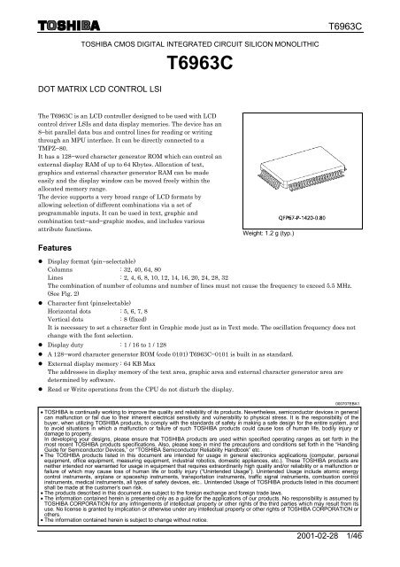
<strong>T6963C</strong>TOSHIBA CMOS DIGITAL INTEGRATED CIRCUIT SILICON MONOLITHIC<strong>T6963C</strong>DOT MATRIX LCD CONTROL LSIThe <strong>T6963C</strong> is an LCD controller designed to be used with LCDcontrol driver LSIs and data display memories. The device has an8−bit parallel data bus and control lines for reading or writingthrough an MPU interface. It can be directly connected to aTMPZ−80.It has a 128−word character generator ROM which can control anexternal display RAM of up to 64 Kbytes. Allocation of text,graphics and external character generator RAM can be madeeasily and the display window can be moved freely within theallocated memory range.The device supports a very broad range of LCD formats byallowing selection of different combinations via a set ofprogrammable inputs. It can be used in text, graphic andcombination text−and−graphic modes, and includes variousattribute functions.Weight: 1.2 g (typ.)Features• Display format (pin−selectable)Columns : 32, 40, 64, 80Lines : 2, 4, 6, 8, 10, 12, 14, 16, 20, 24, 28, 32The combination of number of columns and number of lines must not cause the frequency to exceed 5.5 MHz.(See Fig. 2)• Character font (pinselectable)Horizontal dots : 5, 6, 7, 8Vertical dots: 8 (fixed)It is necessary to set a character font in Graphic mode just as in Text mode. The oscillation frequency does notchange with the font selection.• Display duty : 1 / 16 to 1 / 128• A 128−word character generator ROM (code 0101) <strong>T6963C</strong>−0101 is built in as standard.• External display memory : 64 KB MaxThe addresses in display memory of the text area, graphic area and external character generator area aredetermined by software.• Read or Write operations from the CPU do not disturb the display.000707EBA1• TOSHIBA is continually working to improve the quality and reliability of its products. Nevertheless, semiconductor devices in generalcan malfunction or fail due to their inherent electrical sensitivity and vulnerability to physical stress. It is the responsibility of thebuyer, when utilizing TOSHIBA products, to comply with the standards of safety in making a safe design for the entire system, andto avoid situations in which a malfunction or failure of such TOSHIBA products could cause loss of human life, bodily injury ordamage to property.In developing your designs, please ensure that TOSHIBA products are used within specified operating ranges as set forth in themost recent TOSHIBA products specifications. Also, please keep in mind the precautions and conditions set forth in the “HandlingGuide for Semiconductor Devices,” or “TOSHIBA Semiconductor Reliability Handbook” etc..• The TOSHIBA products listed in this document are intended for usage in general electronics applications (computer, personalequipment, office equipment, measuring equipment, industrial robotics, domestic appliances, etc.). These TOSHIBA products areneither intended nor warranted for usage in equipment that requires extraordinarily high quality and/or reliability or a malfunction orfailure of which may cause loss of human life or bodily injury (“Unintended Usage”). Unintended Usage include atomic energycontrol instruments, airplane or spaceship instruments, transportation instruments, traffic signal instruments, combustion controlinstruments, medical instruments, all types of safety devices, etc.. Unintended Usage of TOSHIBA products listed in this documentshall be made at the customer’s own risk.• The products described in this document are subject to the foreign exchange and foreign trade laws.• The information contained herein is presented only as a guide for the applications of our products. No responsibility is assumed byTOSHIBA CORPORATION for any infringements of intellectual property or other rights of the third parties which may result from itsuse. No license is granted by implication or otherwise under any intellectual property or other rights of TOSHIBA CORPORATION orothers.• The information contained herein is subject to change without notice.2001-02-28 1/46
<strong>T6963C</strong>• A crystal oscillator circuit is built in. The oscillation frequency is adjusted according to the display size. If usingan external clock, use the XI pin as the clock input. (XO open.)External capacitors Crystal oscillation : 20 to 30 pFCeramic oscillation : 30 to 100 pFBuilt−in feedback resistor: 900 kΩ (typ.)• <strong>Toshiba</strong> LCD driver LSIs (other than these with a built−in RAM) can be connected to the device.• External display RAM must be static RAM. The <strong>T6963C</strong> cannot refresh D−RAM.• The attribute functions can only be used in Text mode. They cannot be used in Graphic or CombinationCharacter mode.Block Diagram2001-02-28 2/46
<strong>T6963C</strong>Pin AssignmentPin FunctionsPin Name I / O FunctionsPins for selection of LCD sizeDUAL H H H H H H H H L L L L L L L LMDSMD0MD1InputMDS L L L L H H H H L L L L H H H HMD1 H H L L H H L L H H L L H H L LMD0 H L H L H L H L H L H L H L H LLINES 2 4 6 8 10 12 14 16 4 8 12 16 20 24 28 32V−DOTS 16 32 48 64 80 96 112 128 32 64 96 128 160 192 224 2561 SCREEN 2 SCREENSMD2 H L H LMD2MD3InputPins for selection of number of columnsMD3 H H L LColumns 32 40 64 80FS0 H L H LFS0FS1InputPins for selection of fontFS1 H H L LFont 5 × 8 6 × 8 7 × 8 8 × 8D0 to D7 I / O Data I / O pins between CPU and <strong>T6963C</strong> (D7 is MSB)WR Input Data Write. Write data into <strong>T6963C</strong> when WR = L.RD Input Data Read. Read data from<strong>T6963C</strong> when RD = L.CE Input Chip Enable for <strong>T6963C</strong>. CE must be L when CPU communicates with <strong>T6963C</strong>.2001-02-28 3/46
<strong>T6963C</strong>Pin Name I / O FunctionsC / DInputWR = L ······ C / D = H: Command WriteRD = L ······ C / D = H: Status ReadC / D = L: Data WriteC / D = L: Data ReadHALT Input H ······ Normal, L ······ Stops the oscillation of the clockRESETDSPONInputOutputH ······ Normal (<strong>T6963C</strong> has internal pull−up resistor)L ······ Initialize <strong>T6963C</strong>. Text and graphic have addresses and text and graphic area settings areretained.Control pin for external DC / DC. DSPON is L when HALT is L or RESET is L.(When DSPON goes H, the column drivers are cleared.)DUALInputH ······ Single−ScanL ······ Dual−ScanDUAL H H L LSDSEL H L H LH ······ Sending data by odd / even separationL ······ Sending data by simple serial methodSDSELInputUpper screen HOD, ED ED HOD, ED EDLower screen ― ― LOD, ED EDce0(LOD)ce1(LSCP)OutputOutputce0 at DUAL = H Chip enable pin for display memory in the address range 0000H to 07FFHLOD at DUAL = L Serial data output for odd columns in lower area of LCDce1 at DUAL = H Chip enable pin for display memory in the address range 0800H to 0FFFHLSCP at DUAL = L Shift clock pulse output for column drivers in lower area of LCDce Output Chip enable pin for display memory of any addressd0 to d7 I / O Data I / O pins for display memoryad0 to ad15OutputAddress outputs for display memory(ad15 = L: for upper area of LCD, ad15 = H: for lower area of LCD)R / W Output Read / Write signal for display memoryEDOutputSDSEL = H: Data output for even columns in both upper and lower areas of LCDSDSEL = L: Data output for columns in both upper and lower areas of LCDHOD Output Data output for odd columns in upper area of LCDCDATA Output Synchronous signal for row driverHSCP Output Shift clock pulse for column driver of upper area of LCDLP Output Latch pulse for column driver. Shift clock pulse for row driverFR Output Frame signalXI Input Crystal oscillator inputXO Output Crystal oscillator outputCH1, CH2 Output Check signalT1, T2 Input Test input. Usually openV DD ― Power supply (5.0 V)V SS ― Power supply (0 V)2001-02-28 4/46
<strong>T6963C</strong>● State after RESET / HALT (Fig. 1)Terminal Halt ResetD0 to D7 F Fd0 to d7 F Fr / w H Hce H (Note 1) H (Note 1)ad0 to ad15 H (Note 2) H (Note 2)ce0 , ce1 H (Note 1) H (Note 1)ED, HOD Final data Final dataHSCP L LLP L LCDATA H HFR H HCH1 L K0CH2 L VENDDSPON L LXO H OSC clockH : Level HL : Level LF : Floating (high impedance)K0 : Test signalVEND : Test signalNote 1: In Attribute mode, H or L according to state of graphic pointerNote 2: In Attribute mode, data of graphic pointer2001-02-28 6/46
● The relationship between number of row / column and oscillation clock (Fig. 2)The frequency of the crystal oscillator is adjusted by the following formula.fOSC : Frequency of oscillationfSCP : Frequency of shift clock (fSCP = fOSC / 2)fR : Frequency of FrameM : Number of characters on one line (number of dots on one line 8 M)For all font sizes (e.g. 7 × 8, 6 × 8, 5× 8) the oscillation frequency remains constant.N : Number of rows (duty = 1 / 8N)8M 1× 8N =f SCP f RfOSC = fR × 64 × 2 × M × N(fR = 60 Hz)<strong>T6963C</strong>N246810121416MUnit: [MHz]32 40 64 80 Duty0.492 0.614 0.983 1.2291 / 160.983 1.229 1.966 2.4580.983 1.229 1.966 2.4581 / 321.966 2.458 3.932 4.9151.475 1.843 2.949 3.6861 / 482.949 3.686 5.898 7.3721.966 2.458 3.932 4.9151 / 643.932 4.915 7.864 9.8302.458 3.072 4.915 6.1441 / 804.915 6.144 9.830 12.2882.949 3.686 5.898 7.3731 / 965.898 7.373 11.776 14.7463.440 4.300 6.881 8.6021 / 1126.881 8.601 13.763 17.2033.932 4.915 7.864 9.8301 / 1287.864 9.830 15.729 19.660Note 1: Upper ··· Single−Scan, lower ···· Dual−Scan at f R = 60 HzUpperLower2001-02-28 7/46
● RAM Interface<strong>T6963C</strong>The external RAM is used to store display data (text, graphic and external CG data).With single−scan, text data, graphic data and external CG data can be freely allocated to the memory area(64 KB max).With dual−scan, LCD I is allocated to 0000H to 7FFFH (32 KB max), LCD II is allocated to 8000H to FFFFH(32 KB max). Text data, graphic data and external CG data can be freely allocated in LCD I. In LCDII, thesame addresses must be allocated as in LCD I, except ad15. ad15 determines selection of LCD I or LCD II.It can be use the address decoded signals ce0 (0000 to 07FFH), ce1 (0800 to 0FFFH) within 4 KB.ce0 and ce1 allow decoding of addresses in the ranges (0000 to 07FFH) and (0800 to 0FFFH) respectivelywithin a 4−KB memory space.(Example)(1) Single−Scan (2) Dual−Scan2001-02-28 8/46
<strong>T6963C</strong>● Flowchart of communications with MPU(1) Status ReadA status check must be performed before data is read or written.Status checkThe Status of <strong>T6963C</strong> can be read from the data lines.RD LWR HCE LC / D HD0 to D7 Status wordThe <strong>T6963C</strong> status word format is as follows:MSBLSBSTA7D7STA6D6STA5D5STA4D4STA3D3STA2D2STA1D1STA0D0STA0STA1STA2STA3STA4STA5STA6STA7Check command execution capabilityCheck data read / write capabilityCheck Auto mode data read capabilityCheck Auto mode data write capabilityNot usedCheck controller operation capabilityError flag. Used for Screen Peek and Screen copy commands.Check the blink condition0: Disable1: Enable0: Disable1: Enable0: Disable1: Enable0: Disable1: Enable0: Disable1: Enable0: No error1: Error0: Display off1: Normal displayNote 1: It is necessary to check STA0 and STA1 at the same time.There is a possibility of erroneous operation due to a hardware interrupt.Note 2: For most modes STA0 / STA1 are used as a status check.Note 3: STA2 and STA3 are valid in Auto mode; STA0 and STA1 are invalid.2001-02-28 9/46
<strong>T6963C</strong>Status checking flowa) b)Note 4: When using the MSB = 0 command, a Status Read must be performed.If a status check is not carried out, the <strong>T6963C</strong> cannot operate normally, even after a delay time.The hardware interrupt occurs during the address calculation period (at the end of each line).If a MSB = 0 command is sent to the <strong>T6963C</strong> during this period, the <strong>T6963C</strong> enters Wait status.If a status check is not carried out in this state before the next command is sent, there is thepossibility that the command or data will not be received.(2) Setting dataWhen using the <strong>T6963C</strong>, first set the data, then set the command.Procedure for sending a commanda) The case of 1 data b) The case of 2 dataNote: When sending more than two data, the last datum (or last two data) is valid.2001-02-28 10/46
<strong>T6963C</strong>Command DefinitionsCommand Code D1 D2 FunctionREGISTERS SETTINGSET CONTROL WORDMODE SETDISPLAY MODECURSOR PATTERNSELECTDATA AUTO READ /WRITEDATA READ / WRITE001000010010001000100100010000000100000101000010010000111000X0001000X0011000X0111000X10010000XXX10001XXX100100001001XX101001XX11100101XX100110XX100111XX1010000010100001101000101010001110100100101001011010011010100111101100001011000110110010110000001100000111000010110000111100010011000101X addressDataLow addressLow addressColumnsLow addressColumns―――――――――――――――――――――――Data―Data―Data―Y address00HHigh addressHigh address00HHigh address00H―――――――――――――――――――――――Set Cursor PointerSet Offset RegisterSet Address PointerSet Text Home AddressSet Text AreaSet Graphic Home AddressSet Graphic AreaOR modeEXOR modeAND modeText Attribute modeInternal CG ROM modeExternal CG RAM modeDisplay offCursor on, blink offCursor on, blink onText on, graphic offText off, graphic onText on, graphic on1−line cursor2−line cursor3−line cursor4−line cursor5−line cursor6−line cursor7−line cursor8−line cursorSet Data Auto WriteSet Data Auto ReadAuto ResetSCREEN PEEK 11100000 ― ― Screen PeekSCREEN COPY 11101000 Screen Copy――――――Data Write and Increment ADPData Read and Increment ADPData Write and Decrement ADPData Read and Decrement ADPData Write and Nonvariable ADPData Read and Nonvariable ADPX: invalid2001-02-28 11/46
<strong>T6963C</strong>Command Code D1 D2 FunctionBIT SET / RESET11110XXX11111XXX1111X0001111X0011111X0101111X0111111X1001111X1011111X1101111X111――――――――――――――――――――Bit ResetBit SetBit 0 (LSB)Bit 1Bit 2Bit 3Bit 4Bit 5Bit 6Bit 7 (MSB)X: invalid● Setting registersCode Hex. Function D1 D200100001 21H SET CURSOR POINTER X ADRS Y ADRS00100010 22H SET OFFSET REGISTER DATA 00H00100100 24H SET ADDRESS POINTER LOW ADRS HIGH ADRS(1) Set Cursor PointerThe position of the cursor is specified by X ADRS and Y ADRS. The cursor position can only be moved bythis command. Data read / write from the MPU never changes the cursor pointer. X ADRS and Y ADRSare specified as follows.X ADRS 00H to 4FH (lower 7 bits are valid)Y ADRS 00H to 1FH (lower 5 bits are valid)a) Single− ScanX ADRS 00 to 4FHb) Dual− ScanX ADRS 00H to 4FHY ADRS 00H to 0FHY ADRS 00H to 0FHUpper screenY ADRS 10H to 1FHLower screen(2) Set Offset RegisterThe offset register is used to determine the external character generator RAM area.The <strong>T6963C</strong> has a 16−bit address bus as follows:MSBLSBad15 ad14 ad13 ad12 ad11 ad10 ad9 ad8 ad7 ad6 ad5 ad4 ad3 ad2 ad1 ad0Offset Register Data Character Code Line Scan2001-02-28 12/46
<strong>T6963C</strong><strong>T6963C</strong> assign External character generator, when character code set 80H to FFH in using internalcharacter generator. Character code 00H to 80H assign External character generator, when Externalgenerator mode.The senior five bits define the start address in external memory of the CG RAM area. The next eightbits represent the character code of the character. In internal CG ROM mode, character codes 00H to7FH represent the predefined “internal” CG ROM characters, and codes 80H to FFH represent the user’s own “external” characters. In external CG RAM mode, all 256 codes from 00H to FFH can be used torepresent the user' s own characters. The three least significant bits indicate one of the eight rows ofeight dots that define the character’ s shape.The relationship between display RAM address and offset registerOffset register dataCG RAM hex. address (start to end)00000 0000 to 07FFH00001 0800 to 0FFFH00010 1000 to 17FFH11100 E000 to E7FFH11101 E800 to EFFFH11110 F000 to F7FFH11111 F800 to FFFFH(Example 1)Offset register02HCharacter code80HCharacter generator RAM start address 0001 0100 0000 00001 4 0 0 H(Example 2) The relationship between display RAM data and display charactersγ and ζ are displayed by character generator RAM.2001-02-28 13/46
(3) Set Address Pointer<strong>T6963C</strong>The Set Address Pointer command is used to indicate the start address for writing to (or reading from)external RAM.The Flowchart for Set Address Pointer command● Set Control WordCode Hex. Function D1 D201000000 40H Set Text Home Address Low address High address01000001 41H Set Text Area Columns 00H01000010 42H Set Graphic Home Address Low address High address01000011 43H Set Graphic Area Columns 00HThe home address and column size are defined by this command.2001-02-28 14/46
(1) Set Text Home Address<strong>T6963C</strong>The starting address in the external display RAM for text display is defined by this command. The texthome address indicates the leftmost and uppermost position.The relationship between external display RAM address and display positionTHTH +TA(TH + TA) + TA(TH + 2TA) +TATH + CLTH + TA + CLTH + 2TA + CLTH + 3TA + CLTH + (n − 1) TATH + (n − 1) TA + CLTH: Text home addressTA: Text area number (columns)CL: Columns are fixed by hardware (pin−programmable).(Example)Text home address: 0000HText area: 0020HMD2 = H, MD3 = H: 32 columnsDUAL = H, MDS = L, MD0 = L, MD1 = H : 4 lines0000H 0001H 001EH 001FH0020H 0021H 003EH 002FH0040H 0041H 005EH 005FH0060H 0061H 007EH 007FH(2) Set Graphic Home AddressThe starting address of the external display RAM used for graphic display is defined by this command.The graphic home address indicates the leftmost and uppermost position.The relationship between external display RAM address and display positionGHGH + GA(GH + GA) + GA(GH + 2GA) + GAGH + CLGH + GA + CLGH + 2GA + CLGH + 3GA + CLGH + (n − 1) GAGH + (n − 1) GA + CLGH: Graphic home addressGA: Graphic area number (columns)CL: Columns are fixed by hardware (pin−programmable).2001-02-28 15/46
<strong>T6963C</strong>(Example)Graphic home address: 0000HGraphic area: 0020HMD2 = H, MD3 = H: 32 columnsDUAL = H, MDS = L, MD0 = H, MD1 = H : 2 lines0000H 0001H 001EH 001FH0020H 0021H 003EH 003FH0040H 0041H 005EH 005FH0060H 0061H 007EH 007FH0080H 0081H 009EH 009FH00A0H 00A1H 00BEH 00BFH00C0H 00C1H 00DEH 00DFH00E0H 00E1H 00FEH 00FFH0100H 0101H 011EH 011FH0120H 0121H 013EH 013FH0140H 0141H 015EH 015FH0160H 0161H 017EH 017FH0180H 0181H 019EH 019FH01A0H 01A1H 01BEH 01BFH01C0H 01C1H 01DEH 01DFH01E0H 01E1H 01FEH 01FFH(3) Set Text AreaThe display columns are defined by the hardware setting. This command can be used to adjust thecolumns of the display.(Example)LCD size: 20 columns, 4 linesText home address: 0000HText area: 0014HMD2 = H, MD3 = H: 32 columnsDUAL = H, MDS = L, MD0 = L, MD1 = H : 4 lines0000 0001 ········· 0013 0014 ········· 001F0014 0015 ········· 0027 0028 ········· 00330028 0029 ········· 003B 003C ········· 0047003C 003D ········· 004F 0050 ········· 005BLCD2001-02-28 16/46
Pulido, Alberto L. University of San Diego.The Impact of Immigration Policy on Chicana/o Dreams of Higher Education:Case Studies of Central and Northern CaliforniaJimenez, Patsy. CSU Sacramento. “Dreamers Social Integration Via Public Policy.”Lucia, Leon. CSU Sacramento. “Social Structure and Personality Framework:Immigration Systems, Legality, and Educational and Employment Aspirations.”Rodriguez, Rodolfo. CSU Sacramento. “From the Fields to College: An Analysis ofCollege Aspirations among Latino Farm Workers.”Barajas, Manuel. CSU Sacramento. “The Impact of Immigration Politics onChicana/o Faculty in Higher Education: An Intersectional Analysis of a NorthernCalifornia Case.”Roundtable: NACCS 2015 COMPAS/Rene Nunez Caucus Panel: Anti ImperialistStruggles, Radicalism, and the Political Role of Chicana/o Studies ScholarshipArce, Sean. University of Arizona.Contreras, Raoul Contreras. Indiana Northwest University.Romero, Francisco. Raza Press and Media Association.Chair: Moreno, Jose G. Michigan State University and Estralla Mountain Co.Workshop: Strategies for Collection of Local Oral Histories in ChicanoCommunities.Martinez, Ramon. Retired Educator.Mora‐Torres, Gregorio. San Jose State University.Discussant: Chacon, Rigo. Broadcast Journalist.Chican@s Reading the Mixtec‐Nahua Codices: Unpacking TransnationalInterdisciplinary Inquiry & NEH InstitutesDiaz Martin, Esther. University of Texas, Austin. “Reading Pre‐Hispanic Codices:An Anti‐Colonialist Approach.”Carrillo, Teresa. San Francisco State University. “Reading and Teaching Mixtec‐Nahua Codices as a Brilliant Response to Ethnic and Linguistic Diversity.”Perez Saiz, Sallie. Fresno City College. “A Chicana View on the Politics ofResearch.”Espinoza Watson, Matt. Fresno City College. “In Pursuit of Method:Accountability, Pedagogy, & Perspective in the Study of Mesoamerican Codices.”Some cancelations/additions of panels and/or presenters are not reflected in this copy.
<strong>T6963C</strong>● Cursor pattern selectCode Function Operand10100000 1−line cursor ―10100001 2−line cursor ―10100010 3−line cursor ―10100011 4−line cursor ―10100100 5−line cursor ―10100101 6−line cursor ―10100110 7−line cursor ―10100111 8−line cursor ―When cursor display is ON, this command selects the cursor pattern in the range 1 line to 8 lines. The cursoraddress is defined by the Cursor Pointer Set command.● Data Auto Read / WriteCode Hex. Function Operand10110000 B0H Set Data Auto Write ―10110001 B1H Set Data Auto Read ―10110010 B2H Auto Reset ―This command is convenient for sending a full screen of data from the external display RAM. After settingAuto mode, a Data Write (or Read) command is need not be sent between each datum. A Data Auto Write (orRead) command must be sent after a Set Address Pointer command. After this command, the address pointeris automatically incremented by 1 after each datum. In Auto mode, the <strong>T6963C</strong> cannot accept any othercommands.The Auto Reset command must be sent to the <strong>T6963C</strong> after all data has been sent, to clear Auto mode.2001-02-28 20/46
<strong>T6963C</strong>Note: A Status check for Auto mode(STA2, STA3 should be checked between sending of each datum. Auto Reset should be performed afterchecking STA3 = 1 (STA2 = 1). Refer to the following flowchart.a) Auto Read mode b) Auto Write mode2001-02-28 21/46
<strong>T6963C</strong>● Data Read / WriteCode Hex. Function Operand11000000 C0H Data Write and Increment ADP Data11000001 C1H Data Read and Increment ADP ―11000010 C2H Data Write and Decrement ADP Data11000011 C3H Data Read and Decrement ADP ―11000100 C4H Data Write and Nonvariable ADP Data11000101 C5H Data Read and Nonvariable ADP ―This command is used for writing data from the MPU to external display RAM, and reading data fromexternal display RAM to the MPU. Data Write / Data Read should be executed after setting address usingSet Address Pointer command. The address pointer can be automatically incremented or decremented usingthis command.Note: This command is necessary for each 1−byte datum.Refer to the following flowchart.2001-02-28 22/46
<strong>T6963C</strong>● Screen PeekCode Hex. Function Operand11100000 E0H Screen Peek ―This command is used to transfer 1 byte of displayed data to the data stack; this byte can then be read fromthe MPU by data access. The logical combination of text and graphic display data on the LCD screen can beread by this command.The status (STA6) should be checked just after the Screen Peek command. If the address determined by theSet Address Pointer command is not in the graphic area, this command is ignored and a status flag (STA6) isset.Refer to the following flowchart.Note: This command is available when hardware column number and software column number are the same.Hardware column number is related to MD2 and MD3 setting.Software column number is related to Set Text Area and Set Graphic Area command.2001-02-28 23/46
<strong>T6963C</strong>● Screen CopyCode Hex. Function Operand11101000 E8H Screen Copy ―This command copies a single raster line of data to the graphic area.The start point must be set using the Set Address Pointer command.Note 1: If the attribute function is being used, this command is not available.(With Attribute data is graphic area data.)Note 2: With Dual−Scan, this command cannot be used (because the <strong>T6963C</strong> cannot separate the upper screendata and lower screen data).Refer to the following flowchart.Note: This command is available when hardware column number and software column number are the same.Hardware column number is related to MD2 and MD3 setting.Software column number is related to Set Text Area and Set Graphic Area command.2001-02-28 24/46
<strong>T6963C</strong>● Bit Set / ResetCode Function Operand11110XXX Bit Reset ―11111XXX Bit Set ―1111X000 Bit 0 (LSB) ―1111X001 Bit 1 ―1111X010 Bit 2 ―1111X011 Bit 3 ―1111X100 Bit 4 ―1111X101 Bit 5 ―1111X110 Bit 6 ― X: invalid1111X111 Bit 7 (MSB) ―This command use to set or reset a bit of the byte specified by the address pointer. Only one bit can be set /reset at a time.Refer to the following flowchart.2001-02-28 25/46
<strong>T6963C</strong>Character Code MapThe relation between character codes and character pattern (CG ROM TYPE 0101)2001-02-28 26/46
<strong>T6963C</strong>The relation between character codes and character pattern (CG ROM TYPE 0201)2001-02-28 27/46
<strong>T6963C</strong>Absolute Maximum Ratings (Ta = 25°C)Item Symbol Rating UnitSupply Voltage V DD (Note) −0.3 to 7.0 VInput Voltage V IN (Note) −0.3 to V DD + 0.3 VOperating Temperature T opr −20 to 70 °CStorage Temperature T stg −55 to 125 °CNote: Referenced to V SS = 0 V.Electrical CharacteristicsDc CharacteristicsTest Conditions (Unless Otherwise Noted, V SS = 0 V, V DD = 5.0 V ± 10%, Ta = −20 to 75°C)ItemSymbolTestCircuitTest Condition Min Typ. Max Unit Pin NameOperating Voltage V DD ― ― 4.5 5.0 5.5 V V DDInputOutputVoltageVH Level V IH ―DD ― V− 2.2DD V Input pins―L Level V IL― 0 ― 0.8 V Input pinsH Level V OH ―L LevelV OL―V DD− 0.3― V DD V Output pins― 0 ― 0.3 V Output pinsOutputResistanceInput Pull−upResistanceH Level R OH ― V OUT = V DD − 0.5 V ― ― 400 Ω Output pinsL Level R OL ― V OUT = 0.5 V ― ― 400 Ω Output pinsRPU ― ― 50 100 200 kΩ (Note 1)Operating Frequency f OSC ― ― 0.4 ― 5.5 MHzCurrent Consumption(Operating)Current Consumption(Halt)I DD (1)―V DD = 5.0 V (Note 2)f OSC = 3.0 MHz― 3.3 6 mA V DDI DD (2) ― V DD = 5.0 V ― ― 3 µA V DDNote 1: Applied T1, T2 , RESETNote 2: MDS = L, MD0 = L, MD1 = L, MD2 = H, MD3 = H, FS0 = L, FS1 = L, SDSEL = L, DUAL = H,D7 to D0 = LHLHLHLH2001-02-28 28/46
<strong>T6963C</strong>Ac Characteristics● Switching Characteristics (1)Test Conditions (Unless Otherwise Noted, V DD = 5.0 V ± 10%, V SS = 0 V, Ta = −20 to 70°C)Item Symbol Test Conditions Min Max UnitOperating Frequency f SCP Ta = −10~70°C ― 2.75 MHzSCP Pulse Width t CWH , t CWL ― 150 ― nsSCP Rise / Fall Time t r , t f ― ― 30 nsLP Set−up Time t LSU ― 150 290 nsLP Hold Time t LHD ― 5 40 nsData Set−up Time t DSU ― 170 ― nsData Hold Time t DHD ― 80 ― nsFR Delay Time t d ― 0 90 nsCDATA Set−up Time t CSU ― 450 850 nsCDATA Hold Time t CHD ― 450 950 ns2001-02-28 29/46
<strong>T6963C</strong>● Switching Characteristics (2)Bus TimingTest Conditions (Unless Otherwise Noted, V DD = 5.0 V ± 10%, V SS = 0 V, Ta = −20 to 75°C)Item Symbol Test Conditions Min Max UnitC / D Set−up Time t CDS ― 100 ― nsC / D Hold Time t CDH ― 10 ― nsCE , RD , WR Pulse Width t CE , t RD , t WR ― 80 ― nsData Set−up Time t DS ― 80 ― nsData Hold Time t DH ― 40 ― nsAccess Time t ACC ― ― 150 nsOutput Hold Time t OH ― 10 50 ns2001-02-28 30/46
<strong>T6963C</strong>● Switching Characteristics (3)(1) External RAM Read mode(2) External RAM Write mode2001-02-28 31/46
<strong>T6963C</strong>Test Conditions (Unless Otherwise Noted, V DD = 5.0 V ± 10%, V SS = 0 V, Ta = −20 to 70°C)Item Symbol Test Conditions Min Max UnitAddress Delay Time t d1 ― ― 250 nsce Fall Delay Time (Read) t d2 ― ― 180 nsce Rise Delay Time (Read) t d3 ― ― 180 nsData Set−up Time t DS ― 0 ― nsData Hold Time t DH ― 30 ― nsce Fall Delay Time (Write) t d4 ― ― 200 nsce Rise Delay Time (Write) t d5 ― ― 200 nsr / w Fall Delay Time t d6 ― ― 180 nsr / w Rise Delay Time t d7 ― ― 180 nsData Stable Time t d8 ― ― 450 nsData Hold Time t d9 ― ― 200 ns2001-02-28 32/46
<strong>T6963C</strong><strong>T6963C</strong> Example of Application CircuitThe <strong>T6963C</strong> can be directly connected to a TMPZ84C00A (Z80 Note 1: CMOS). The <strong>T6963C</strong> can be used with aTMPZ84C00A as shown in the following application circuit.● MPU memory address mappingData is transferred to the <strong>T6963C</strong> using a memory request signal.AddressDATA (I / O)Command / StatusXXXXHXXXX + 1HNote 1: Z80 is a trademark of Zilog Inc.2001-02-28 33/46
<strong>T6963C</strong>● MPU I / O addressingData is transferred to the <strong>T6963C</strong> using an I / O request signal.I / O AddressDATACommand / StatusXXHXX + 1H2001-02-28 34/46
<strong>T6963C</strong>● When using PPI LSI (TMP82C55)The <strong>T6963C</strong> can be connected to a PPI LSI.The port A connects to the data bus.The port C connects to the control bus. (C / D, CE , WR , RD )2001-02-28 35/46
<strong>T6963C</strong>Application Circuit (1)2001-02-28 36/46
<strong>T6963C</strong>Application Circuit (2)2001-02-28 37/46
<strong>T6963C</strong>Sample Program1 : ; <strong>T6963C</strong> SAMPLE PROGRAM V0.012 : ;3 : ; SOURCE PROGRAM for TMPZ84C00P4 : ; 1991 − 2 −155 : ; Display Size: 20 Column × 8 Lines6 : ;7 : ; Character Font: 8 Dots Mode8 : ;9 : TXHOME EQU 40H ; SET TXT HM ADD10 : TXAREA EQU 41H ; SET TXT AREA11 : GRHOME EQU 42H ; SET GR HM ADD12 : GRAREA EQU 43H ; SET GR AREA13 : OFFSET EQU 22H ; SET OFFSET ADD14 : ADPSET EQU 24H ; SET ADD PTR15 : AWRON EQU 0B0H ; SET AUTO WRITE MODE16 : AWROFF EQU 0B2H ; RESET AUTO WRITE MODE17 : CMDP EQU 01H ; CMD PORT18 : DP EQU 00H ; DATA PORT19 : STACK EQU 9FFFH ; STACK POINTER BASE ADDRESS20 : ;21 : ORG 0000H22 : START:23 : LD SP, STACK24 : ;25 : ; SET TEXT HOME ADDRESS26 : ;27 : LD HL, 0000H ; TEXT HOME ADDRESS 0000H28 : CALL DT229 : LD A, TXHOME30 : CALL CMD31 : ;32 : ; SET GRAPHIC HOME ADDRESS33 : ;34 : LD HL, 0200H ; GRAPHIC HOME ADDRESS 0200H35 : CALL DT236 : LD A, GRHOME37 : CALL CMD38 : ;2001-02-28 38/46
39 : ; SET TEXT AREA40 : ;41 : LD HL, 0014H ; TEXT AREA 20 Columns42 : CALL DT243 : LD A, TXAREA44 : CALL CMD45 : ;46 : ; SET GRAPHIC AREA47 : ;48 : LD HL, 0014H ; GRAPHIC AREA 20 Columns49 : CALL DT250 : LD A, GRAREA51 : CALL CMD52 : ;53 : ; MODE SET (OR MODE, Internal Character Generator MODE)54 : ;55 : LD A,80H56 : CALL CMD57 : ;58 : ; SET OFFSET REGISTER (00010 10000000 000 = 1400H CG RAM START ADDRESS)59 : ; CHARACTER CODE 80H60 : LD HL, 0002H61 : CALL DT262 : LD A, OFFSET63 : CALL CMD64 : ;65 : ; DISPLAY MODE66 : ; (TEXT ON, GRAPHICS OFF, CURSOR OFF)67 : ;68 : LD A, 94H69 : CALL CMD70 : ;71 : ; WRITE TEXT BLANK CODE72 : ;73 : LD HL, 0000H ; SET Address Pointer 0000H74 : CALL DT2 ; (TEXT HOME ADDRESS)75 : LD A, ADPSET76 : CALL CMD77 :78 : LD A, AWRON ; SET DATA AUTO WRITE<strong>T6963C</strong>2001-02-28 39/46
79 : CALL CMD ;80 :81 : LD BC, 00A0H ; 20 Columns × 8Lines (160 = A0H)82 : TXCR:83 : LD A, 00H ; WRITE DATA 00H84 : CALL ADT ; (WRITE BLANK CODE)85 :86 : DEC BC87 : LD A, B88 : OR C89 : JR NZ, TXCR90 :91 : LD A, AWROFF ; AUTO RESET92 : CALL CMD93 :94 : ;95 : ; WRITE EXTERNAL CHARACTER GENERATOR DATA96 : ;97 : LD DE, EXTCG ; CG data address in Program98 : LD HL, 1400H ; CG RAM Start Address (1400H)99 : CALL DT2100 : LD A, ADPSET101 : CALL CMD102 : ;103 : LD A, AWRON ; SET DATA AUTO WRITE104 : CALL CMD105 :106 : LD B, 40H ; 8 Character × 8 byte (64 = 40H)107 : EXCG:108 : LD A, (DE) ; WRITE DATA TO EXTERNAL RAM109 : CALL ADT ;110 : INC HL111 : INC DE112 : DJNZ EXCG113 :114 : LD A, AWROFF ; AUTO RESET115 : CALL CMD116 : ;117 : ; WRITE TEXT DISPLAY DATA (INTERNAL CG)118 : ;<strong>T6963C</strong>2001-02-28 40/46
119 : LD HL, 0040H ; Address Pointer 3 Line, 4 Column120 : CALL DT2121 : LD A, ADPSET122 : CALL CMD123 :124 : LD A, AWRON ; SET DATA AUTO WRITE125 : CALL CMD126 :127 : LD B, 0DH ; 13 Character128 : LD DE, TXPRT129 : TXLP1:130 : LD A, (DE) ; WRITE DATA131 : CALL ADT132 : INC DE133 : DJNZ TXLP1134 :135 : LD A, AWROFF ; AUTO RESET136 : CALL CMD137 : ;138 : ; WRITE TEXT DISPLAY DATA (EXTERNAL CG upper part)139 : ;140 : LD HL, 006CH ; Address Pointer 5 Line, 8 Column141 : CALL DT2142 : LD A, ADPSET143 : CALL CMD144 :145 : LD A, AWRON ; SET DATA AUTO WRITE146 : CALL CMD147 :148 : LD B, 06H ; 6 Character149 : LD DE, EXPRT1150 : TXLP2:151 : LD A, (DE) ; WRITE DATA152 : CALL ADT153 : INC DE154 : DJNZ TXLP2155 :156 : LD A, AWROFF ; AUTO RESET157 : CALL CMD158 : ;<strong>T6963C</strong>2001-02-28 41/46
159 : ; WRITE TEXT DISPLAY DATA (EXTERNAL CG lower part)160 : ;161 : LD HL, 0080H ; Address Pointer 6 Line, 8 Column162 : CALL DT2163 : LD A, ADPSET164 : CALL CMD165 :166 : LD A, AWRON ; SET DATA AUTO WRITE167 : CALL CMD168 :169 : LD B, 06H ; 6 Character170 : LD DE, EXPRT2171 : TXLP3:172 : LD A, (DE) ; WRITE DATA173 : CALL ADT174 : INC DE175 : DJNZ TXLP3176 :177 : LD A, AWROFF ; AUTO RESET178 : CALL CMD179 : PEND:180 : JP PEND ; PROGRAM END181 : ;182 : ; Subroutine start183 : ;184 : ; COMMAND WRITE ROUTINE185 : ;186 : CMD:187 : PUSH AF188 : CMD1: IN A, (CMDP)189 : AND 03H190 : CP 03H ; STATUS CHECK191 : JR NZ, CMD1192 : POP AF193 : OUT (CMDP), A ; WRITE COMMAND194 : RET195 : ;196 : ; DATA WRITE (1 byte) ROUTINE197 : ;198 : DT1:<strong>T6963C</strong>2001-02-28 42/46
<strong>T6963C</strong>199 : PUSH AF200 : DT11: IN A, (CMDP)201 : AND 03H202 : CP 03H ; STATUS CHECK203 : JR NZ, DT11204 : POP AF205 : OUT (DP), A ; WRITE DATA206 : RET207 : ;208 : ; DATA WRITE (2 byte) ROUTINE209 : ;210 : DT2:211 : IN A, (CMDP)212 : AND 03H213 : CP 03H ; STATUS CHECK214 : JR NZ, DT2215 : LD A, L216 : OUT (DP), A ; WRITE DATA (D1)217 : DT21:218 : IN A, (CMDP)219 : AND 03H220 : CP 03H ; STATUS CHECK221 : JR NZ, DT21222 :223 : LD A, H224 : OUT (DP), A ; WRITE DATA (D2)225 : RET226 : ;227 : ; AUTO WRITE MODE ROUTINE228 : ;229 : ADT:230 : PUSH AF231 : ADT1: IN A, (CMDP)232 : AND 08H233 : CP 08H ; STATUS CHECK234 : JR NZ, ADT1235 : POP AF236 : OUT (DP), A ; WRITE DATA237 : RET238 : ;2001-02-28 43/46
<strong>T6963C</strong>239 : ; Subroutine end240 : ;241 : ; TEXT DISPLAY CHARACTER CODE242 : ;243 : TXPRT:244 : DEFB 34H, 00H, 2FH, 00H, 33H, 00H ; INTERNAL CG CODE245 : DEFB 28H, 00H, 29H, 00H, 22H, 00H, 21H246 : EXPRT1:247 : DEFB 80H, 81H, 00H, 00H, 84H, 85H ; EXTERNAL CG CODE248 : EXPRT2:249 : DEFB 82H, 83H, 00H, 00H, 86H, 87H250 : ;251 : ; EXTERNAL CG FONT DATA252 : ;253 : EXTCG:254 : ;255 : ; upper / left CHARACTER CODE 80H256 : DEFB 01H, 01H, 0FFH, 01H, 3FH, 21H, 3FH, 21H257 :258 : ; upper / right CHARACTER CODE 81H259 : DEFB 00H, 00H, 0FFH, 00H, 0FCH, 04H, 0FCH, 04H260 :261 : ; lower/left CHARACTER CODE 82H262 : DEFB 21H, 3FH, 05H, 0DH, 19H, 31H, 0E1H, 01H263 :264 : ; lower/right CHARACTER CODE 83H265 : DEFB 04H, 0FCH, 40H, 60H, 30H, 1CH, 07H, 00H266 :267 : ; upper/left CHARACTER CODE 84H268 : DEFB 08H, 08H, 0FFH, 08H, 09H, 01H, 01H, 7FH269 :270 : ; upper/right CHARACTER CODE 85H271 : DEFB 10H, 10H, 0FFH, 10H, 10H, 00H, 00H, 0FCH272 :273 : ; lower/left CHARACTER CODE 86H274 : DEFB 00H, 00H, 00H, 01H, 07H, 3CH, 0E7H, 00H275 :276 : ; lower/right CHARACTER CODE 87H277 : DEFB 18H, 30H, 60H, 0C0H, 00H, 00H, 0E0H, 3FH278 : ;279 : END2001-02-28 44/46
<strong>T6963C</strong>Display Sample2001-02-28 45/46
<strong>T6963C</strong>Package Dimensions2001-02-28 46/46