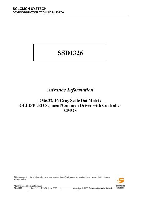
SSD1326 - Display Future
SSD1326 - Display Future
SSD1326 - Display Future
- No tags were found...

You also want an ePaper? Increase the reach of your titles
YUMPU automatically turns print PDFs into web optimized ePapers that Google loves.
10.2 GRAPHIC ACCELERATION COMMAND..................................................................................................................4810.2.1 Horizontal Scrolling by Window (26h) .......................................................................................................4810.2.2 Deactivate Horizontal Scroll (2Eh) ............................................................................................................4810.2.3 Activate Horizontal Scroll (2Fh).................................................................................................................4811 MAXIMUM RATINGS.......................................................................................................... 4912 DC CHARACTERISTICS..................................................................................................... 5013 AC CHARACTERISTICS..................................................................................................... 5114 APPLICATION EXAMPLES ............................................................................................... 5615 PACKAGE INFORMATION................................................................................................ 5715.1 <strong>SSD1326</strong>U DETAIL DIMENSION ..........................................................................................................................5715.2 <strong>SSD1326</strong>U1 DETAIL DIMENSION ........................................................................................................................60<strong>SSD1326</strong> Rev 1.2 P 3/63 Jul 2008 Solomon Systech
TABLES22. REVISE RES# TIMING IN TABLE 3-1 : AC CHARACTERISTICS (CHANGE TO 2US FROM 1US)............................................ITABLE 5-1 : <strong>SSD1326</strong>Z BUMP DIE PAD COORDINATES.......................................................................................................10TABLE 6-1 : PIN DESCRIPTIONS ...........................................................................................................................................12TABLE 7-1 : <strong>SSD1326</strong>U PIN ASSIGNMENT TABLE...............................................................................................................15TABLE 7-2 : <strong>SSD1326</strong>U1 PIN ASSIGNMENT TABLE.............................................................................................................17TABLE 8-1 : MCU INTERFACE ASSIGNMENT UNDER DIFFERENT BUS INTERFACE MODE .......................................................18TABLE 8-2 : CONTROL PINS OF SERIAL INTERFACE..............................................................................................................22TABLE 8-3 : CONTROL PINS OF 6800 INTERFACE..................................................................................................................23TABLE 8-4 : CONTROL PINS OF 8080 INTERFACE..................................................................................................................24TABLE 9-1 : COMMAND TABLE............................................................................................................................................33TABLE 11-1 : MAXIMUM RATINGS (VOLTAGE REFERENCED TO V SS ) ..................................................................................49TABLE 12-1 : DC CHARACTERISTICS...................................................................................................................................50TABLE 13-1 : AC CHARACTERISTICS...................................................................................................................................51TABLE 13-2 : I 2 C INTERFACE TIMING CHARACTERISTICS....................................................................................................52TABLE 13-3 : SERIAL INTERFACE TIMING CHARACTERISTICS..............................................................................................53TABLE 13-4 : 6800-SERIES MCU PARALLEL INTERFACE TIMING CHARACTERISTICS..........................................................54TABLE 13-5 : 8080-SERIES MCU PARALLEL INTERFACE TIMING CHARACTERISTICS..........................................................55Solomon Systech Jul 2008 P 4/63 Rev 1.2 <strong>SSD1326</strong>
1 GENERAL DESCRIPTION<strong>SSD1326</strong> is a single-chip CMOS OLED/PLED driver with controller for 16 gray scale levels organic /polymer light emitting diode dot-matrix graphic display system. <strong>SSD1326</strong> consists of 256 segments, 32commons. This IC is designed for Common Cathode type OLED / PLED panel.<strong>SSD1326</strong> displays data directly from its internal 256 x 32 x 4 bits Graphic Data RAM (GDDRAM).Data/Commands are sent from general MCU through the hardware selectable I 2 C Interface, 6800-/8080-series compatible Parallel Interface or Serial Peripheral Interface.2 FEATURES• Support max. 256 x 32 matrix panel• Power supply: V DD = 2.4V -3.5VV DDIO = 1.7V - V DDV CC = 9.0V - 15.0V• OLED driving output voltage, 15V maximum• Maximum segment source current: 100uA• Dual Common maximum sink current: 25mA• Embedded 256 x 32 x 4 bit SRAM display buffer• 256 steps contrast current control• Selectable to either 16 gray scale or mono display• Internal oscillator• Programmable frame rate• Continuous horizontal scrolling with flexible scrolling window• Pin selectable MCU interfaceo I 2 C interfaceo 8-bit 6800-series parallel interfaceo 8-bit 8080-series parallel interfaceo Serial Peripheral Interface• Wide range of operating temperature: -40 to 85 °C3 ORDERING INFORMATIONTable 3-1: Ordering InformationOrdering Part Number SEG COMPackageFormReference<strong>SSD1326</strong>Z 256 32 dual COG Page 8<strong>SSD1326</strong>U 256 32 dual COF Page 14 ,57<strong>SSD1326</strong>U1 256 32 dual COF Page 16, 60RemarkMin SEG pad pitch : 40.08umMin COM pad pitch : 45um− Punched COF, Sn plating− This package is for I 2 C interface and theslave address is set as b0111100(SA0=0).− SEG lead pitch 0.11mm x0.999=0.10989mm− COM lead pitch 0.11mmx0.999=0.10989mm− Punched COF, Au plating− This package is for I 2 C interface and theslave address is set as b0111100(SA0=0).− SEG lead pitch 0.11mm x0.999=0.10989mm− COM lead pitch 0.11mmx0.999=0.10989mmSolomon Systech Jul 2008 P 6/63 Rev 1.2 <strong>SSD1326</strong>
4 BLOCK DIAGRAMFigure 4-1 : <strong>SSD1326</strong> Block DiagramRES#CS#D/C#E(RD#)R/W# (WR#)BS0BS1BS2D7D6D5D4D3SDA OUT /D2SDA IN /SD IN /D1SCL/SCLK/D0V DDV DDIOV SSV LSSGPIO0MCUInterfaceCommandDecoderOscillator<strong>Display</strong>TimingGeneratorGDDRAMSEG/COM DrivingBlockGray Scale DecoderCommon Drivers Segment Drivers Common Drivers.................................COMA0|COMA31SEG0|SEG255COMB0|COMB31CLCLSFRVCIRVCCVCOMHIREF<strong>SSD1326</strong> Rev 1.2 P 7/63 Jul 2008 Solomon Systech
5 DIE PAD FLOOR PLANFigure 5-1 : <strong>SSD1326</strong>Z Die DrawingPad 1Alignment key X-pos Y-pos SizeT shape -5145.000 0.000 75um x 75um+ shape 5145.000 0.000 75um x 75umDie sizeDie thicknessMin I/O pad pitchMin SEG pad pitchMin COM pad pitchBump height Nominal10620um x 1210um457um +/- 25um65um40.08um45um15um<strong>SSD1326</strong>ZBump SizePad# X(um) Y(um)188-315, 319-446 28 64.3316-318, 28 64.32-33, 149-180 32 56.2634, 148 32 56.2636-146 42 5535, 147 42 55187, 447 50 64.31,181 50 56.26182-186, 448-452 50 64.3YPad# 447Pad#1Bump pad face up<strong>SSD1326</strong>Pad#187Pad#181XSolomon Systech Jul 2008 P 8/63 Rev 1.2 <strong>SSD1326</strong>
Figure 5-2 : <strong>SSD1326</strong>Z Alignment Mark Dimensions<strong>SSD1326</strong> Rev 1.2 P 9/63 Jul 2008 Solomon Systech
Table 5-1 : <strong>SSD1326</strong>Z Bump Die Pad CoordinatesPad# Signal X-pos Y-pos Pad# Signal X-pos Y-pos Pad# Signal X-pos Y-pos1 DUMMY -5245 -536.87 81 VCC -649.74 -537.5 161 COMA19 4312.86 -536.872 COMB0 -5167.86 -536.87 82 VDDIO -584.74 -537.5 162 COMA18 4357.86 -536.873 COMB1 -5122.86 -536.87 83 VDDIO -519.74 -537.5 163 COMA17 4402.86 -536.874 COMB2 -5077.86 -536.87 84 VDDIO -454.74 -537.5 164 COMA16 4447.86 -536.875 COMB3 -5032.86 -536.87 85 VSS -389.74 -537.5 165 COMA15 4492.86 -536.876 COMB4 -4987.86 -536.87 86 GPIO0 -324.74 -537.5 166 COMA14 4537.86 -536.877 COMB5 -4942.86 -536.87 87 VDDIO -259.74 -537.5 167 COMA13 4582.86 -536.878 COMB6 -4897.86 -536.87 88 BS0 -194.74 -537.5 168 COMA12 4627.86 -536.879 COMB7 -4852.86 -536.87 89 VSS -129.74 -537.5 169 COMA11 4672.86 -536.8710 COMB8 -4807.86 -536.87 90 VSS -64.74 -537.5 170 COMA10 4717.86 -536.8711 COMB9 -4762.86 -536.87 91 VSS 0.26 -537.5 171 COMA9 4762.86 -536.8712 COMB10 -4717.86 -536.87 92 VSS 65.26 -537.5 172 COMA8 4807.86 -536.8713 COMB11 -4672.86 -536.87 93 BS1 130.26 -537.5 173 COMA7 4852.86 -536.8714 COMB12 -4627.86 -536.87 94 VDDIO 195.26 -537.5 174 COMA6 4897.86 -536.8715 COMB13 -4582.86 -536.87 95 BS2 260.26 -537.5 175 COMA5 4942.86 -536.8716 COMB14 -4537.86 -536.87 96 VSS 325.26 -537.5 176 COMA4 4987.86 -536.8717 COMB15 -4492.86 -536.87 97 FR 390.26 -537.5 177 COMA3 5032.86 -536.8718 COMB16 -4447.86 -536.87 98 CL 455.26 -537.5 178 COMA2 5077.86 -536.8719 COMB17 -4402.86 -536.87 99 VDDIO 520.26 -537.5 179 COMA1 5122.86 -536.8720 COMB18 -4357.86 -536.87 100 CS# 585.26 -537.5 180 COMA0 5167.86 -536.8721 COMB19 -4312.86 -536.87 101 RES# 650.26 -537.5 181 DUMMY 5245 -536.8722 COMB20 -4267.86 -536.87 102 D/C# 715.26 -537.5 182 DUMMY 5245 -114.7523 COMB21 -4222.86 -536.87 103 VSS 780.26 -537.5 183 DUMMY 5245 -24.7524 COMB22 -4177.86 -536.87 104 R/W#(WR#) 845.26 -537.5 184 DUMMY 5245 65.2525 COMB23 -4132.86 -536.87 105 E(RD#) 910.26 -537.5 185 DUMMY 5245 155.2526 COMB24 -4087.86 -536.87 106 VDDIO 975.26 -537.5 186 DUMMY 5245 245.2527 COMB25 -4042.86 -536.87 107 VDDIO 1040.26 -537.5 187 DUMMY 5245 465.1528 COMB26 -3997.86 -536.87 108 VDD 1105.26 -537.5 188 SEG0 5170.26 465.1529 COMB27 -3952.86 -536.87 109 VDD 1170.26 -537.5 189 SEG1 5130.18 465.1530 COMB28 -3907.86 -536.87 110 VCC 1235.26 -537.5 190 SEG2 5090.1 465.1531 COMB29 -3862.86 -536.87 111 VCC 1300.26 -537.5 191 SEG3 5050.02 465.1532 COMB30 -3817.86 -536.87 112 VCC 1365.26 -537.5 192 SEG4 5009.94 465.1533 COMB31 -3772.86 -536.87 113 VLSS 1430.26 -537.5 193 SEG5 4969.86 465.1534 DUMMY -3727.86 -536.87 114 VLSS 1495.26 -537.5 194 SEG6 4929.78 465.1535 DUMMY -3639.74 -537.5 115 VDDIO 1560.26 -537.5 195 SEG7 4889.7 465.1536 VCC -3574.74 -537.5 116 VSS 1625.26 -537.5 196 SEG8 4849.62 465.1537 VCC -3509.74 -537.5 117 D0 1690.26 -537.5 197 SEG9 4809.54 465.1538 VCC -3444.74 -537.5 118 D1 1755.26 -537.5 198 SEG10 4769.46 465.1539 VCOMH -3379.74 -537.5 119 D2 1820.26 -537.5 199 SEG11 4729.38 465.1540 VCOMH -3314.74 -537.5 120 D3 1885.26 -537.5 200 SEG12 4689.3 465.1541 VCOMH -3249.74 -537.5 121 VSS 1950.26 -537.5 201 SEG13 4649.22 465.1542 IREF -3184.74 -537.5 122 D4 2015.26 -537.5 202 SEG14 4609.14 465.1543 VLSS -3119.74 -537.5 123 D5 2080.26 -537.5 203 SEG15 4569.06 465.1544 VLSS -3054.74 -537.5 124 D6 2145.26 -537.5 204 SEG16 4528.98 465.1545 VLSS -2989.74 -537.5 125 D7 2210.26 -537.5 205 SEG17 4488.9 465.1546 VDD -2924.74 -537.5 126 VSS 2275.26 -537.5 206 SEG18 4448.82 465.1547 VDD -2859.74 -537.5 127 CLS 2340.26 -537.5 207 SEG19 4408.74 465.1548 VDDIO -2794.74 -537.5 128 VDDIO 2405.26 -537.5 208 SEG20 4368.66 465.1549 VDDIO -2729.74 -537.5 129 VDDIO 2470.26 -537.5 209 SEG21 4328.58 465.1550 VDDIO -2664.74 -537.5 130 VDD 2535.26 -537.5 210 SEG22 4288.5 465.1551 VDDIO -2599.74 -537.5 131 VDD 2600.26 -537.5 211 SEG23 4248.42 465.1552 VSS -2534.74 -537.5 132 VDD 2665.26 -537.5 212 SEG24 4208.34 465.1553 TR8 -2469.74 -537.5 133 VSS 2730.26 -537.5 213 SEG25 4168.26 465.1554 TR7 -2404.74 -537.5 134 VSS 2795.26 -537.5 214 SEG26 4128.18 465.1555 TR6 -2339.74 -537.5 135 VLSS 2860.26 -537.5 215 SEG27 4088.1 465.1556 TR5 -2274.74 -537.5 136 VLSS 2925.26 -537.5 216 SEG28 4048.02 465.1557 VSS -2209.74 -537.5 137 VLSS 2990.26 -537.5 217 SEG29 4007.94 465.1558 TR4 -2144.74 -537.5 138 VCOMH 3055.26 -537.5 218 SEG30 3967.86 465.1559 TR3 -2079.74 -537.5 139 VCOMH 3120.26 -537.5 219 SEG31 3927.78 465.1560 TR2 -2014.74 -537.5 140 VCOMH 3185.26 -537.5 220 SEG32 3887.7 465.1561 TR1 -1949.74 -537.5 141 VCC 3250.26 -537.5 221 SEG33 3847.62 465.1562 TR0 -1884.74 -537.5 142 VCC 3315.26 -537.5 222 SEG34 3807.54 465.1563 VLSS -1819.74 -537.5 143 VCC 3380.26 -537.5 223 SEG35 3767.46 465.1564 VLSS -1754.74 -537.5 144 VCC 3445.26 -537.5 224 SEG36 3727.38 465.1565 VLSS -1689.74 -537.5 145 VCC 3510.26 -537.5 225 SEG37 3687.3 465.1566 VSS -1624.74 -537.5 146 VCC 3575.26 -537.5 226 SEG38 3647.22 465.1567 VSS -1559.74 -537.5 147 DUMMY 3640.26 -537.5 227 SEG39 3607.14 465.1568 VSS -1494.74 -537.5 148 DUMMY 3727.86 -536.87 228 SEG40 3567.06 465.1569 BGGND -1429.74 -537.5 149 COMA31 3772.86 -536.87 229 SEG41 3526.98 465.1570 VBREF -1364.74 -537.5 150 COMA30 3817.86 -536.87 230 SEG42 3486.9 465.1571 VCIR -1299.74 -537.5 151 COMA29 3862.86 -536.87 231 SEG43 3446.82 465.1572 VCIR -1234.74 -537.5 152 COMA28 3907.86 -536.87 232 SEG44 3406.74 465.1573 VCIR -1169.74 -537.5 153 COMA27 3952.86 -536.87 233 SEG45 3366.66 465.1574 VCIR -1104.74 -537.5 154 COMA26 3997.86 -536.87 234 SEG46 3326.58 465.1575 VDD -1039.74 -537.5 155 COMA25 4042.86 -536.87 235 SEG47 3286.5 465.1576 VDD -974.74 -537.5 156 COMA24 4087.86 -536.87 236 SEG48 3246.42 465.1577 VDD -909.74 -537.5 157 COMA23 4132.86 -536.87 237 SEG49 3206.34 465.1578 VDD -844.74 -537.5 158 COMA22 4177.86 -536.87 238 SEG50 3166.26 465.1579 VCC -779.74 -537.5 159 COMA21 4222.86 -536.87 239 SEG51 3126.18 465.1580 VCC -714.74 -537.5 160 COMA20 4267.86 -536.87 240 SEG52 3086.1 465.15Solomon Systech Jul 2008 P 10/63 Rev 1.2 <strong>SSD1326</strong>
Pad# Signal X-pos Y-pos Pad# Signal X-pos Y-pos Pad# Signal X-pos Y-pos241 SEG53 3046.02 465.15 321 SEG130 -160.38 465.15 401 SEG210 -3366.78 465.15242 SEG54 3005.94 465.15 322 SEG131 -200.46 465.15 402 SEG211 -3406.86 465.15243 SEG55 2965.86 465.15 323 SEG132 -240.54 465.15 403 SEG212 -3446.94 465.15244 SEG56 2925.78 465.15 324 SEG133 -280.62 465.15 404 SEG213 -3487.02 465.15245 SEG57 2885.7 465.15 325 SEG134 -320.7 465.15 405 SEG214 -3527.1 465.15246 SEG58 2845.62 465.15 326 SEG135 -360.78 465.15 406 SEG215 -3567.18 465.15247 SEG59 2805.54 465.15 327 SEG136 -400.86 465.15 407 SEG216 -3607.26 465.15248 SEG60 2765.46 465.15 328 SEG137 -440.94 465.15 408 SEG217 -3647.34 465.15249 SEG61 2725.38 465.15 329 SEG138 -481.02 465.15 409 SEG218 -3687.42 465.15250 SEG62 2685.3 465.15 330 SEG139 -521.1 465.15 410 SEG219 -3727.5 465.15251 SEG63 2645.22 465.15 331 SEG140 -561.18 465.15 411 SEG220 -3767.58 465.15252 SEG64 2605.14 465.15 332 SEG141 -601.26 465.15 412 SEG221 -3807.66 465.15253 SEG65 2565.06 465.15 333 SEG142 -641.34 465.15 413 SEG222 -3847.74 465.15254 SEG66 2524.98 465.15 334 SEG143 -681.42 465.15 414 SEG223 -3887.82 465.15255 SEG67 2484.9 465.15 335 SEG144 -721.5 465.15 415 SEG224 -3927.9 465.15256 SEG68 2444.82 465.15 336 SEG145 -761.58 465.15 416 SEG225 -3967.98 465.15257 SEG69 2404.74 465.15 337 SEG146 -801.66 465.15 417 SEG226 -4008.06 465.15258 SEG70 2364.66 465.15 338 SEG147 -841.74 465.15 418 SEG227 -4048.14 465.15259 SEG71 2324.58 465.15 339 SEG148 -881.82 465.15 419 SEG228 -4088.22 465.15260 SEG72 2284.5 465.15 340 SEG149 -921.9 465.15 420 SEG229 -4128.3 465.15261 SEG73 2244.42 465.15 341 SEG150 -961.98 465.15 421 SEG230 -4168.38 465.15262 SEG74 2204.34 465.15 342 SEG151 -1002.06 465.15 422 SEG231 -4208.46 465.15263 SEG75 2164.26 465.15 343 SEG152 -1042.14 465.15 423 SEG232 -4248.54 465.15264 SEG76 2124.18 465.15 344 SEG153 -1082.22 465.15 424 SEG233 -4288.62 465.15265 SEG77 2084.1 465.15 345 SEG154 -1122.3 465.15 425 SEG234 -4328.7 465.15266 SEG78 2044.02 465.15 346 SEG155 -1162.38 465.15 426 SEG235 -4368.78 465.15267 SEG79 2003.94 465.15 347 SEG156 -1202.46 465.15 427 SEG236 -4408.86 465.15268 SEG80 1963.86 465.15 348 SEG157 -1242.54 465.15 428 SEG237 -4448.94 465.15269 SEG81 1923.78 465.15 349 SEG158 -1282.62 465.15 429 SEG238 -4489.02 465.15270 SEG82 1883.7 465.15 350 SEG159 -1322.7 465.15 430 SEG239 -4529.1 465.15271 SEG83 1843.62 465.15 351 SEG160 -1362.78 465.15 431 SEG240 -4569.18 465.15272 SEG84 1803.54 465.15 352 SEG161 -1402.86 465.15 432 SEG241 -4609.26 465.15273 SEG85 1763.46 465.15 353 SEG162 -1442.94 465.15 433 SEG242 -4649.34 465.15274 SEG86 1723.38 465.15 354 SEG163 -1483.02 465.15 434 SEG243 -4689.42 465.15275 SEG87 1683.3 465.15 355 SEG164 -1523.1 465.15 435 SEG244 -4729.5 465.15276 SEG88 1643.22 465.15 356 SEG165 -1563.18 465.15 436 SEG245 -4769.58 465.15277 SEG89 1603.14 465.15 357 SEG166 -1603.26 465.15 437 SEG246 -4809.66 465.15278 SEG90 1563.06 465.15 358 SEG167 -1643.34 465.15 438 SEG247 -4849.74 465.15279 SEG91 1522.98 465.15 359 SEG168 -1683.42 465.15 439 SEG248 -4889.82 465.15280 SEG92 1482.9 465.15 360 SEG169 -1723.5 465.15 440 SEG249 -4929.9 465.15281 SEG93 1442.82 465.15 361 SEG170 -1763.58 465.15 441 SEG250 -4969.98 465.15282 SEG94 1402.74 465.15 362 SEG171 -1803.66 465.15 442 SEG251 -5010.06 465.15283 SEG95 1362.66 465.15 363 SEG172 -1843.74 465.15 443 SEG252 -5050.14 465.15284 SEG96 1322.58 465.15 364 SEG173 -1883.82 465.15 444 SEG253 -5090.22 465.15285 SEG97 1282.5 465.15 365 SEG174 -1923.9 465.15 445 SEG254 -5130.3 465.15286 SEG98 1242.42 465.15 366 SEG175 -1963.98 465.15 446 SEG255 -5170.38 465.15287 SEG99 1202.34 465.15 367 SEG176 -2004.06 465.15 447 DUMMY -5245 465.15288 SEG100 1162.26 465.15 368 SEG177 -2044.14 465.15 448 DUMMY -5245 245.25289 SEG101 1122.18 465.15 369 SEG178 -2084.22 465.15 449 DUMMY -5245 155.25290 SEG102 1082.1 465.15 370 SEG179 -2124.3 465.15 450 DUMMY -5245 65.25291 SEG103 1042.02 465.15 371 SEG180 -2164.38 465.15 451 DUMMY -5245 -24.75292 SEG104 1001.94 465.15 372 SEG181 -2204.46 465.15 452 DUMMY -5245 -114.75293 SEG105 961.86 465.15 373 SEG182 -2244.54 465.15294 SEG106 921.78 465.15 374 SEG183 -2284.62 465.15295 SEG107 881.7 465.15 375 SEG184 -2324.7 465.15296 SEG108 841.62 465.15 376 SEG185 -2364.78 465.15297 SEG109 801.54 465.15 377 SEG186 -2404.86 465.15298 SEG110 761.46 465.15 378 SEG187 -2444.94 465.15299 SEG111 721.38 465.15 379 SEG188 -2485.02 465.15300 SEG112 681.3 465.15 380 SEG189 -2525.1 465.15301 SEG113 641.22 465.15 381 SEG190 -2565.18 465.15302 SEG114 601.14 465.15 382 SEG191 -2605.26 465.15303 SEG115 561.06 465.15 383 SEG192 -2645.34 465.15304 SEG116 520.98 465.15 384 SEG193 -2685.42 465.15305 SEG117 480.9 465.15 385 SEG194 -2725.5 465.15306 SEG118 440.82 465.15 386 SEG195 -2765.58 465.15307 SEG119 400.74 465.15 387 SEG196 -2805.66 465.15308 SEG120 360.66 465.15 388 SEG197 -2845.74 465.15309 SEG121 320.58 465.15 389 SEG198 -2885.82 465.15310 SEG122 280.5 465.15 390 SEG199 -2925.9 465.15311 SEG123 240.42 465.15 391 SEG200 -2965.98 465.15312 SEG124 200.34 465.15 392 SEG201 -3006.06 465.15313 SEG125 160.26 465.15 393 SEG202 -3046.14 465.15314 SEG126 120.18 465.15 394 SEG203 -3086.22 465.15315 SEG127 80.1 465.15 395 SEG204 -3126.3 465.15316 DUMMY 40.02 465.15 396 SEG205 -3166.38 465.15317 DUMMY -0.06 465.15 397 SEG206 -3206.46 465.15318 DUMMY -40.14 465.15 398 SEG207 -3246.54 465.15319 SEG128 -80.22 465.15 399 SEG208 -3286.62 465.15320 SEG129 -120.3 465.15 400 SEG209 -3326.7 465.15<strong>SSD1326</strong> Rev 1.2 P 11/63 Jul 2008 Solomon Systech
6 PIN DESCRIPTIONKey:I = InputO =OutputIO = Bi-directional (input/output)P = Power pinNC = Not ConnectedPull LOW= connect to GroundPull HIGH= connect to V DDIOPin NamePin Type DescriptionTable 6-1 : Pin DescriptionsRES# I This pin is reset signal input. When the pin is LOW, initialization of the chip is executed.Keep this pin HIGH during normal operation.CS# I This pin is the chip select input. The chip is enabled for MCU communication only whenCS# is pulled LOW.D/C# I This pin is Data/Command control pin. When the pin is pulled HIGH and serial interfacemode is selected, the data at SD IN is treated as data. When the pin is pulled LOW, the dataat SD IN will be transferred to the command register. In I 2 C mode, this pin acts as SA0 forslave address selection.E (RD#) I This pin is MCU interface input. When interfacing to a 6800-series microprocessor, this pinwill be used as the Enable (E) signal. Read/write operation is initiated when this pin ispulled HIGH and the chip is selected.When connecting to an 8080-microprocessor, this pin receives the Read (RD#) signal. Dataread operation is initiated when this pin is pulled LOW and the chip is selected.R/W# (WR#) I This pin is MCU interface input. When interfacing to a 6800-series microprocessor, this pinwill be used as Read/Write (R/W#) selection input. Read mode will be carried out when thispin is pulled HIGH and write mode will be carried out when LOW.When 8080 interface mode is selected, this pin will be the Write (WR#) input. Data writeoperation is initiated when this pin is pulled LOW and the chip is selected.D[7:0] IO These is 8-bit bi-directional data bus to be connected to the microprocessor’s data bus.When serial interface mode is selected, D1 will be the serial data input, SD IN , and D 0 will bethe serial clock input, SCLK.When I 2 C mode is selected, D2, D1 should be tied together and serve as SDA out , SDA in inapplication and D0 is the serial clock input, SCL.BS[2:0] I MCU bus interface selection pins.Pin NameI 2 CInterface6800-parallelinterface(8 bit)8080-parallelinterface(8 bit)BS0 0 0 0 0BS1 1 0 1 0BS2 0 1 1 0SerialinterfaceV DDIO P This pin is a power supply pin of I/O buffer. It should be connected to V DD or externalsource. All I/O signal should have voltage high reference to V DDIO . When I/O signal pins(BS0, CLS, CL, interface signals…) pull HIGH, they should be connected to V DDIO .V DD P Power Supply pin. It must be connected to external source.V SS, V LSS P These pins are ground pin and also act as ground reference for the logic pins. They must beconnected to external ground.Solomon Systech Jul 2008 P 12/63 Rev 1.2 <strong>SSD1326</strong>
Pin Name Pin Type DescriptionCL I This is external clock input pin.When internal clock is enabled (i.e. HIGH in CLS pin), this pin is not used and should beconnected to V SS . When internal clock is disabled (i.e. LOW in CLS pin), this pin is theexternal clock source input pin.CLS I This pin is internal clock enable. When this pin is pulled HIGH, internal oscillator isselected.The internal clock will be disabled when it is pulled LOW, an external clock source must beconnected to CL pin for normal operation.V CC P This is the most positive voltage supply pin of the chip. It is supplied either by external highvoltage source.V COMH P A capacitor should be connected between this pin and V SS .V CIR O This is a reserved pin. It should be kept NC (i.e. Float during normal operation).FR O This pin outputs RAM write synchronization signal. Proper timing between MCU datawriting and frame display timing can be achieve to prevent tearing effect.Keep NC if not used.GPIO0 IO This is reserved pin. It should be kept NC (i.e. Float during normal operation).I REF I This pin is the segment output current reference pin. I SEG is derived from I REF . A resistorshould be connected between this pin and V SS to maintain the current around 10uA.V BREF - This is a reserved pin. It should be floated.BGGND P This is a reserved pin. It should be connected to V SS .TR[8:0] - This is a reserved pin. It should be floated.COM0 ~COM31SEG0 ~SEG255OOThese pins provide the Common switch signals to the OLED panel. These pins are in highimpedance state when display is OFF.<strong>SSD1326</strong> is in dual COM:COM0 = COMA0 and COMB0.COM1 = COMA1 and COMB1.COM2 = COMA2 and COMB2.:COM29 = COMA29 and COMB29.COM30 = COMA30 and COMB30.COM31 = COMA31 and COMB31These pins provide the OLED segment driving signals. These pins are in high impedancestate when display is OFF.Dummy - Dummy pin.<strong>SSD1326</strong> Rev 1.2 P 13/63 Jul 2008 Solomon Systech
7 PIN ARRANGEMENT7.1 <strong>SSD1326</strong>U pin assignmentFigure 7-1 : <strong>SSD1326</strong>U Pin AssignmentSolomon Systech Jul 2008 P 14/63 Rev 1.2 <strong>SSD1326</strong>
Table 7-1 : <strong>SSD1326</strong>U Pin Assignment TablePin No. Pin Name Pin No. Pin Name Pin No. Pin Name Pin No. Pin Name Pin No. Pin Name1 VCC 81 SEG230 161 SEG150 241 SEG70 321 NC2 VCOMH 82 SEG229 162 SEG149 242 SEG69 322 NC3 NC 83 SEG228 163 SEG148 243 SEG68 323 COMA04 SDA 84 SEG227 164 SEG147 244 SEG67 324 COMA15 SCL 85 SEG226 165 SEG146 245 SEG66 325 COMA26 RES# 86 SEG225 166 SEG145 246 SEG65 326 COMA37 VDDIO 87 SEG224 167 SEG144 247 SEG64 327 COMA48 VDD 88 SEG223 168 SEG143 248 SEG63 328 COMA59 VSS 89 SEG222 169 SEG142 249 SEG62 329 COMA610 IREF 90 SEG221 170 SEG141 250 SEG61 330 COMA711 NC 91 SEG220 171 SEG140 251 SEG60 331 COMA812 NC 92 SEG219 172 SEG139 252 SEG59 332 COMA913 COMB31 93 SEG218 173 SEG138 253 SEG58 333 COMA1014 COMB30 94 SEG217 174 SEG137 254 SEG57 334 COMA1115 COMB29 95 SEG216 175 SEG136 255 SEG56 335 COMA1216 COMB28 96 SEG215 176 SEG135 256 SEG55 336 COMA1317 COMB27 97 SEG214 177 SEG134 257 SEG54 337 COMA1418 COMB26 98 SEG213 178 SEG133 258 SEG53 338 COMA1519 COMB25 99 SEG212 179 SEG132 259 SEG52 339 COMA1620 COMB24 100 SEG211 180 SEG131 260 SEG51 340 COMA1721 COMB23 101 SEG210 181 SEG130 261 SEG50 341 COMA1822 COMB22 102 SEG209 182 SEG129 262 SEG49 342 COMA1923 COMB21 103 SEG208 183 SEG128 263 SEG48 343 COMA2024 COMB20 104 SEG207 184 SEG127 264 SEG47 344 COMA2125 COMB19 105 SEG206 185 SEG126 265 SEG46 345 COMA2226 COMB18 106 SEG205 186 SEG125 266 SEG45 346 COMA2327 COMB17 107 SEG204 187 SEG124 267 SEG44 347 COMA2428 COMB16 108 SEG203 188 SEG123 268 SEG43 348 COMA2529 COMB15 109 SEG202 189 SEG122 269 SEG42 349 COMA2630 COMB14 110 SEG201 190 SEG121 270 SEG41 350 COMA2731 COMB13 111 SEG200 191 SEG120 271 SEG40 351 COMA2832 COMB12 112 SEG199 192 SEG119 272 SEG39 352 COMA2933 COMB11 113 SEG198 193 SEG118 273 SEG38 353 COMA3034 COMB10 114 SEG197 194 SEG117 274 SEG37 354 COMA3135 COMB9 115 SEG196 195 SEG116 275 SEG36 355 NC36 COMB8 116 SEG195 196 SEG115 276 SEG35 356 NC37 COMB7 117 SEG194 197 SEG114 277 SEG3438 COMB6 118 SEG193 198 SEG113 278 SEG3339 COMB5 119 SEG192 199 SEG112 279 SEG3240 COMB4 120 SEG191 200 SEG111 280 SEG3141 COMB3 121 SEG190 201 SEG110 281 SEG3042 COMB2 122 SEG189 202 SEG109 282 SEG2943 COMB1 123 SEG188 203 SEG108 283 SEG2844 COMB0 124 SEG187 204 SEG107 284 SEG2745 NC 125 SEG186 205 SEG106 285 SEG2646 NC 126 SEG185 206 SEG105 286 SEG2547 NC 127 SEG184 207 SEG104 287 SEG2448 NC 128 SEG183 208 SEG103 288 SEG2349 NC 129 SEG182 209 SEG102 289 SEG2250 NC 130 SEG181 210 SEG101 290 SEG2151 NC 131 SEG180 211 SEG100 291 SEG2052 NC 132 SEG179 212 SEG99 292 SEG1953 NC 133 SEG178 213 SEG98 293 SEG1854 NC 134 SEG177 214 SEG97 294 SEG1755 NC 135 SEG176 215 SEG96 295 SEG1656 SEG255 136 SEG175 216 SEG95 296 SEG1557 SEG254 137 SEG174 217 SEG94 297 SEG1458 SEG253 138 SEG173 218 SEG93 298 SEG1359 SEG252 139 SEG172 219 SEG92 299 SEG1260 SEG251 140 SEG171 220 SEG91 300 SEG1161 SEG250 141 SEG170 221 SEG90 301 SEG1062 SEG249 142 SEG169 222 SEG89 302 SEG963 SEG248 143 SEG168 223 SEG88 303 SEG864 SEG247 144 SEG167 224 SEG87 304 SEG765 SEG246 145 SEG166 225 SEG86 305 SEG666 SEG245 146 SEG165 226 SEG85 306 SEG567 SEG244 147 SEG164 227 SEG84 307 SEG468 SEG243 148 SEG163 228 SEG83 308 SEG369 SEG242 149 SEG162 229 SEG82 309 SEG270 SEG241 150 SEG161 230 SEG81 310 SEG171 SEG240 151 SEG160 231 SEG80 311 SEG072 SEG239 152 SEG159 232 SEG79 312 NC73 SEG238 153 SEG158 233 SEG78 313 NC74 SEG237 154 SEG157 234 SEG77 314 NC75 SEG236 155 SEG156 235 SEG76 315 NC76 SEG235 156 SEG155 236 SEG75 316 NC77 SEG234 157 SEG154 237 SEG74 317 NC78 SEG233 158 SEG153 238 SEG73 318 NC79 SEG232 159 SEG152 239 SEG72 319 NC80 SEG231 160 SEG151 240 SEG71 320 NC<strong>SSD1326</strong> Rev 1.2 P 15/63 Jul 2008 Solomon Systech
7.2 <strong>SSD1326</strong>U1 pin assignmentFigure 7-2 : <strong>SSD1326</strong>U1 Pin AssignmentSolomon Systech Jul 2008 P 16/63 Rev 1.2 <strong>SSD1326</strong>
Table 7-2 : <strong>SSD1326</strong>U1 Pin Assignment TablePin No. Pin Name Pin No. Pin Name Pin No. Pin Name Pin No. Pin Name Pin No. Pin Name1 VCC 81 SEG230 161 SEG150 241 SEG70 321 NC2 VCOMH 82 SEG229 162 SEG149 242 SEG69 322 NC3 NC 83 SEG228 163 SEG148 243 SEG68 323 COMA04 SDA 84 SEG227 164 SEG147 244 SEG67 324 COMA15 SCL 85 SEG226 165 SEG146 245 SEG66 325 COMA26 RES# 86 SEG225 166 SEG145 246 SEG65 326 COMA37 VDD 87 SEG224 167 SEG144 247 SEG64 327 COMA48 NC 88 SEG223 168 SEG143 248 SEG63 328 COMA59 VSS 89 SEG222 169 SEG142 249 SEG62 329 COMA610 IREF 90 SEG221 170 SEG141 250 SEG61 330 COMA711 NC 91 SEG220 171 SEG140 251 SEG60 331 COMA812 NC 92 SEG219 172 SEG139 252 SEG59 332 COMA913 COMB31 93 SEG218 173 SEG138 253 SEG58 333 COMA1014 COMB30 94 SEG217 174 SEG137 254 SEG57 334 COMA1115 COMB29 95 SEG216 175 SEG136 255 SEG56 335 COMA1216 COMB28 96 SEG215 176 SEG135 256 SEG55 336 COMA1317 COMB27 97 SEG214 177 SEG134 257 SEG54 337 COMA1418 COMB26 98 SEG213 178 SEG133 258 SEG53 338 COMA1519 COMB25 99 SEG212 179 SEG132 259 SEG52 339 COMA1620 COMB24 100 SEG211 180 SEG131 260 SEG51 340 COMA1721 COMB23 101 SEG210 181 SEG130 261 SEG50 341 COMA1822 COMB22 102 SEG209 182 SEG129 262 SEG49 342 COMA1923 COMB21 103 SEG208 183 SEG128 263 SEG48 343 COMA2024 COMB20 104 SEG207 184 SEG127 264 SEG47 344 COMA2125 COMB19 105 SEG206 185 SEG126 265 SEG46 345 COMA2226 COMB18 106 SEG205 186 SEG125 266 SEG45 346 COMA2327 COMB17 107 SEG204 187 SEG124 267 SEG44 347 COMA2428 COMB16 108 SEG203 188 SEG123 268 SEG43 348 COMA2529 COMB15 109 SEG202 189 SEG122 269 SEG42 349 COMA2630 COMB14 110 SEG201 190 SEG121 270 SEG41 350 COMA2731 COMB13 111 SEG200 191 SEG120 271 SEG40 351 COMA2832 COMB12 112 SEG199 192 SEG119 272 SEG39 352 COMA2933 COMB11 113 SEG198 193 SEG118 273 SEG38 353 COMA3034 COMB10 114 SEG197 194 SEG117 274 SEG37 354 COMA3135 COMB9 115 SEG196 195 SEG116 275 SEG36 355 NC36 COMB8 116 SEG195 196 SEG115 276 SEG35 356 NC37 COMB7 117 SEG194 197 SEG114 277 SEG3438 COMB6 118 SEG193 198 SEG113 278 SEG3339 COMB5 119 SEG192 199 SEG112 279 SEG3240 COMB4 120 SEG191 200 SEG111 280 SEG3141 COMB3 121 SEG190 201 SEG110 281 SEG3042 COMB2 122 SEG189 202 SEG109 282 SEG2943 COMB1 123 SEG188 203 SEG108 283 SEG2844 COMB0 124 SEG187 204 SEG107 284 SEG2745 NC 125 SEG186 205 SEG106 285 SEG2646 NC 126 SEG185 206 SEG105 286 SEG2547 NC 127 SEG184 207 SEG104 287 SEG2448 NC 128 SEG183 208 SEG103 288 SEG2349 NC 129 SEG182 209 SEG102 289 SEG2250 NC 130 SEG181 210 SEG101 290 SEG2151 NC 131 SEG180 211 SEG100 291 SEG2052 NC 132 SEG179 212 SEG99 292 SEG1953 NC 133 SEG178 213 SEG98 293 SEG1854 NC 134 SEG177 214 SEG97 294 SEG1755 NC 135 SEG176 215 SEG96 295 SEG1656 SEG255 136 SEG175 216 SEG95 296 SEG1557 SEG254 137 SEG174 217 SEG94 297 SEG1458 SEG253 138 SEG173 218 SEG93 298 SEG1359 SEG252 139 SEG172 219 SEG92 299 SEG1260 SEG251 140 SEG171 220 SEG91 300 SEG1161 SEG250 141 SEG170 221 SEG90 301 SEG1062 SEG249 142 SEG169 222 SEG89 302 SEG963 SEG248 143 SEG168 223 SEG88 303 SEG864 SEG247 144 SEG167 224 SEG87 304 SEG765 SEG246 145 SEG166 225 SEG86 305 SEG666 SEG245 146 SEG165 226 SEG85 306 SEG567 SEG244 147 SEG164 227 SEG84 307 SEG468 SEG243 148 SEG163 228 SEG83 308 SEG369 SEG242 149 SEG162 229 SEG82 309 SEG270 SEG241 150 SEG161 230 SEG81 310 SEG171 SEG240 151 SEG160 231 SEG80 311 SEG072 SEG239 152 SEG159 232 SEG79 312 NC73 SEG238 153 SEG158 233 SEG78 313 NC74 SEG237 154 SEG157 234 SEG77 314 NC75 SEG236 155 SEG156 235 SEG76 315 NC76 SEG235 156 SEG155 236 SEG75 316 NC77 SEG234 157 SEG154 237 SEG74 317 NC78 SEG233 158 SEG153 238 SEG73 318 NC79 SEG232 159 SEG152 239 SEG72 319 NC80 SEG231 160 SEG151 240 SEG71 320 NC<strong>SSD1326</strong> Rev 1.2 P 17/63 Jul 2008 Solomon Systech
8 FUNCTIONAL BLOCK DESCRIPTIONS8.1 MCU Interface Selection<strong>SSD1326</strong> MCU interface consist of 8 data pins and 5 control pins. The pin assignment at different interfacemode is summarized in Table 8-1. Different MCU mode can be set by hardware selection on BS[2:0] pins(please refer to Table 6-1 for BS[2:0] setting).Table 8-1 : MCU interface assignment under different bus interface modePin Name Data/Command InterfaceControl SignalBusInterface D7 D6 D5 D4 D3 D2 D1 D0 E R/W# CS# D/C# RES#8-bit 8080 D[7:0] RD# WR# CS# D/C# RES#8-bit 6800 D[7:0] E R/W# CS# D/C# RES#SPI Tie LOW NC SDIN SCLK Tie LOW CS# D/C# RES#I 2 C Tie LOW SDA OUT SDA IN SCL Tie LOW SA0 RES#8.1.1 MCU I 2 C InterfaceThe I 2 C communication interface consists of slave address bit SA0, I 2 C-bus data signal SDA (SDA OUT /D 2 foroutput and SDA IN /D 1 for input) and I 2 C-bus clock signal SCL (D 0 ). Both the data and clock signals must beconnected to pull-up resistors. RES# is used for the initialization of device.a) Slave address bit (SA0)<strong>SSD1326</strong> has to recognize the slave address before transmitting or receiving any information by theI 2 C-bus. The device will respond to the slave address following by the slave address bit (“SA0” bit)and the read/write select bit (“R/W#” bit) with the following byte format,b 7 b 6 b 5 b 4 b 3 b 2 b 1 b 00 1 1 1 1 0 SA0 R/W#“SA0” bit provides an extension bit for the slave address. Either “0111100” or “0111101”, can beselected as the slave address of <strong>SSD1326</strong>. D/C# pin acts as SA0 for slave address selection.“R/W#” bit is used to determine the operation mode of the I 2 C-bus interface. R/W#=1, it is in readmode. R/W#=0, it is in write mode.b) I 2 C-bus data signal (SDA)SDA acts as a communication channel between the transmitter and the receiver. The data and theacknowledgement are sent through the SDA. If SDA in is connected to the “SDA out”, the devicebecomes fully I 2 C bus compatible.It should be noticed that the ITO track resistance and the pulled-up resistance at “SDA” pin becomesa voltage potential divider. As a result, the acknowledgement would not be possible to attain a validlogic 0 level in “SDA”.“SDA IN ” and “SDA OUT ” are tied together and serve as SDA. The “SDA IN ” pin must be connected toact as SDA. The “SDA OUT ” pin may be disconnected. When “SDA OUT ” pin is disconnected, theacknowledgement signal will be ignored in the I 2 C-bus.c) I 2 C-bus clock signal (SCL)The transmission of information in the I 2 C-bus is following a clock signal, SCL. Each transmission ofdata bit is taken place during a single clock period of SCL.Solomon Systech Jul 2008 P 18/63 Rev 1.2 <strong>SSD1326</strong>
8.1.1.1 I2C-bus Write data and read register statusThe I 2 C-bus interface gives access to write data and command into the device. Please refer to Figure 8-1 :I2C-bus data format for the write mode of I 2 C-bus in chronological order.Figure 8-1 : I 2 C-bus data formatWrite modeNote:Co – Continuation bitD/C# – Data / Command Selection bitACK – AcknowledgementSA0 – Slave address bitR/W# – Read / Write Selection bitS – Start Condition / P – Stop ConditionS011110 1 1 1 1 0R/W#SA0D/C#CoACKControl byte Data byte Control byteACKD/C#CoACKACKData byteACKPSlave Address m ≥ 0 words 1 byten ≥ 0 bytesMSB ……………….LSB0 1 1 1 1 0R/W#SA0<strong>SSD1326</strong>Slave AddressD/CCo0 0 0 0 0 0ACKControl byte<strong>SSD1326</strong> Rev 1.2 P 19/63 Jul 2008 Solomon Systech
8.1.1.2 Write mode for I 2 C1) The master device initiates the data communication by a start condition. The definition of the startcondition is shown in Figure 8-2. The start condition is established by pulling the SDA from HIGH toLOW while the SCL stays HIGH.2) The slave address is following the start condition for recognition use. For the <strong>SSD1326</strong>, the slaveaddress is either “b0111100” or “b0111101” by changing the SA0 to LOW or HIGH.3) The write mode is established by setting the R/W# bit to logic “0”.4) An acknowledgement signal will be generated after receiving one byte of data, including the slaveaddress and the R/W# bit. Please refer to the Figure 8-3 for the graphical representation of theacknowledge signal. The acknowledge bit is defined as the SDA line is pulled down during the HIGHperiod of the acknowledgement related clock pulse.5) After the transmission of the slave address, either the control byte or the data byte may be sent acrossthe SDA. A control byte mainly consists of Co and D/C# bits following by six “0” ‘s.a. If the Co bit is set as logic “0”, the transmission of the following information will containdata bytes only.b. The D/C# bit determines the next data byte is acted as a command or a data. If the D/C# bit isset to logic “0”, it defines the following data byte as a command. If the D/C# bit is set to logic“1”, it defines the following data byte as a data which will be stored at the GDDRAM. TheGDDRAM column address pointer will be increased by one automatically after each datawrite.6) Acknowledge bit will be generated after receiving each control byte or data byte.7) The write mode will be finished when a stop condition is applied. The stop condition is also definedin Figure 8-2. The stop condition is established by pulling the “SDA in” from LOW to HIGH whilethe “SCL” stays HIGH.Figure 8-2 : Definition of the Start and Stop Conditiont HSTARTt SSTOPSDASDASCLSPSCLSTART conditionSTOP conditionSolomon Systech Jul 2008 P 20/63 Rev 1.2 <strong>SSD1326</strong>
Figure 8-3 : Definition of the acknowledgement conditionDATA OUTPUTBY TRANSMITTERDATA OUTPUTBY RECEIVERNon-acknowledgeAcknowledgeSCL FROMMASTER1 28 9SSTARTConditionClock pulse for acknowledgementPlease be noted that the transmission of the data bit has some limitations.1. The data bit, which is transmitted during each SCL pulse, must keep at a stable state within the “HIGH”period of the clock pulse. Please refer to the Figure 8-4 for graphical representations. Except in start orstop conditions, the data line can be switched only when the SCL is LOW.2. Both the data line (SDA) and the clock line (SCL) should be pulled up by external resistors.Figure 8-4 : Definition of the data transfer conditionSDASCLData line isstableChange of data<strong>SSD1326</strong> Rev 1.2 P 21/63 Jul 2008 Solomon Systech
8.1.2 MCU Serial InterfaceThe serial interface consists of serial clock SCLK, serial data SD IN , D/C#, CS#.Table 8-2 : Control pins of Serial interfaceFunction E R/W# CS# D/C#Write command Tie LOW Tie LOW L LWrite data Tie LOW Tie LOW L HSD IN is shifted into an 8-bit shift register on every rising edge of SCLK in the order of D7, D6, ... D0. D/C# issampled on every eighth clock and the data byte in the shift register is written to the Graphic <strong>Display</strong> DataRAM (GDDRAM) or command register in the same clock.Under serial mode, only write operations are allowed.CS#Figure 8-5 : Write procedure in SPI modeD/C#SDIN/SCLKDB1 DB2 DBnSCLK(D0)SDIN(D1)D7 D6 D5 D4 D3 D2 D1 D0Solomon Systech Jul 2008 P 22/63 Rev 1.2 <strong>SSD1326</strong>
8.1.3 MCU Parallel 6800-series InterfaceThe parallel interface consists of 8 bi-directional data pins (D[7:0]), R/W#, D/C#, E and CS#.A LOW in R/W# indicates WRITE operation and HIGH in R/W# indicates READ operation.A LOW in D/C# indicates COMMAND read/write and HIGH in D/C# indicates DATA read/write.The E input serves as data latch signal while CS# is LOW. Data is latched at the falling edge of E signal.Note(1)↓ stands for falling edge of signalH stands for HIGH in signalL stands for LOW in signalTable 8-3 : Control pins of 6800 interfaceFunction E R/W# CS# D/C#Write command ↓ L L LRead status ↓ H L LWrite data ↓ L L HRead data ↓ H L HIn order to match the operating frequency of display RAM with that of the microprocessor, some pipelineprocessing is internally performed which requires the insertion of a dummy read before the first actual displaydata read. This is shown in Figure 8-6.Figure 8-6 : Data read back procedure - insertion of dummy readR/W#EDatabusN n n+1 n+2Write columnaddressDummy read Read 1st data Read 2nd data Read 3rd data<strong>SSD1326</strong> Rev 1.2 P 23/63 Jul 2008 Solomon Systech
8.1.4 MCU Parallel 8080-series InterfaceThe parallel interface consists of 8 bi-directional data pins (D[7:0]), RD#, WR#, D/C# and CS#.A LOW in D/C# indicates COMMAND read/write and HIGH in D/C# indicates DATA read/write.A rising edge of RD# input serves as a data READ latch signal while CS# is kept LOW.A rising edge of WR# input serves as a data/command WRITE latch signal while CS# is kept LOW.CS#Figure 8-7 : Example of Write procedure in 8080 parallel interface modeWR#D[7:0]D/C#RD#highlowFigure 8-8 : Example of Read procedure in 8080 parallel interface modeCS#RD#D[7:0]D/C#WR#highlowNote(1) ↑ stands for rising edge of signalH stands for HIGH in signalL stands for LOW in signalTable 8-4 : Control pins of 8080 interfaceFunction RD# WR# CS# D/C#Write command H ↑ L LRead status ↑ H L LWrite data H ↑ L HRead data ↑ H L HSolomon Systech Jul 2008 P 24/63 Rev 1.2 <strong>SSD1326</strong>
In order to match the operating frequency of display RAM with that of the microprocessor, some pipelineprocessing is internally performed which requires the insertion of a dummy read before the first actual displaydata read. This is shown in Figure 8-9.Figure 8-9 : <strong>Display</strong> data read back procedure - insertion of dummy readWR#RD#DatabusN n n+1 n+2Write columnaddressDummy read Read 1st data Read 2nd data Read 3rd data<strong>SSD1326</strong> Rev 1.2 P 25/63 Jul 2008 Solomon Systech
8.2 Segment Drivers/Common DriversSegment drivers have 256 current sources to drive OLED panel. The driving current can be adjusted from 0 to100uA with 8 bits, 256 steps. Common drivers generate voltage scanning pulses. The block diagrams andwaveforms of the segment and common driver are shown as follow.Figure 8-10 : Segment and Common Driver Block DiagramI SEGCurrentDriveResetOLEDPixelV LSSSegment DriverV COMHV COMHNon-selectRowNon-selectRowSelectedRowSelectedRowCommonDriverCOMAV LSSV LSSCommonDriverCOMBThe commons are scanned sequentially, row by row. If a row is not selected, all the pixels on the row are inreverse bias by driving those commons to voltage V COMH as shown in Figure 8-11 .In the scanned row, the pixels on the row will be turned ON or OFF by sending the corresponding data signalto the segment pins. If the pixel is turned OFF, the segment current is kept at 0. On the other hand, thesegment drives to I SEG when the pixel is turned ON.Solomon Systech Jul 2008 P 26/63 Rev 1.2 <strong>SSD1326</strong>
COM0Figure 8-11 : Segment and Common Driver Signal Waveform (Gray scale mode)One Frame PeriodNon-select RowV COMHV LSSCOM1V COMHSelected RowV LSSCOMVoltageThis row is selected to turnONV COMHV LSSSegmentVoltageTimeWaveform for ONV PV LSSWaveform for OFFTime<strong>SSD1326</strong> Rev 1.2 P 27/63 Jul 2008 Solomon Systech
There are four phases to driving an OLED a pixel. In phase 1, the pixel is reset by the segment driver to V LSSin order to discharge the previous data charge stored in the parasitic capacitance along the segment electrode.The period of phase 1 can be programmed by command B1h A[3:0] from 1 to 16 DCLK. An OLED panelwith larger capacitance requires a longer period for discharging.In phase 2, first pre-charge is performed. The pixel is driven to attain the corresponding voltage level V P fromV LSS . The amplitude of V P can be programmed by the command BCh. The period of phase 2 can beprogrammed in length from 1 to 16 DCLK by command B1h A[7:4]. If the capacitance value of the pixel ofOLED panel is larger, a longer period is required to charge up the capacitor to reach the desired voltage.In phase 3, the OLED pixel is driven to the targeted driving voltage through second pre-charge. The secondpre-charge can control the speed of the charging process. The setup of phase 3 can be programmed bycommand BBh.Last phase (phase 4) is current drive stage. The current source in the segment driver delivers constant currentto the pixel. The driver IC employs PWM (Pulse Width Modulation) method to control the gray scale of eachpixel individually. The wider pulse widths in the current drive stage results in brighter pixels and vice versa.This is shown in the following figure.Phase2Figure 8-12: Gray Scale Control by PWM in SegmentSegmentVoltagePhase1Phase3Phase4V PV LSSWider pulse widthdrives pixel brighterOLEDPanelAfter finishing phase 4, the driver IC will go back to phase 1 to display the next row image data. This fourstepcycle is run continuously to refresh image display on OLED panel.The length of phase 4 is defined by command B7h “Select Default Gray Scale Table” or B8h “Set Gray ScaleTable”. In the table, the gray scale is defined in incremental way, with reference to the length of previoustable entry.Solomon Systech Jul 2008 P 28/63 Rev 1.2 <strong>SSD1326</strong>
8.3 Oscillator Circuit and <strong>Display</strong> Time GeneratorFigure 8-13 : Oscillator Circuit and <strong>Display</strong> Time GeneratorCLInternalOscillatorFoscMUXCLKDividerDCLK<strong>Display</strong>ClockCLSThis module is an On-Chip low power RC oscillator circuitry. The operation clock (CLK) can be generatedeither from internal oscillator or external source CL pin. This selection is done by CLS pin. If CLS pin ispulled HIGH, internal oscillator is chosen and CL should be connected to V SS . Pulling CLS pin LOWdisables internal oscillator and external clock must be connected to CL pins for proper operation. When theinternal oscillator is selected, its output frequency F OSC can be changed by command B3h, please refer toTable 9-1.The display clock (DCLK) for the <strong>Display</strong> Timing Generator is derived from CLK. The division factor “D”can be programmed from 1 to 16 by command B3hDCLK = F OSC / DThe frame frequency of display is determined by the following formula.FoscFFRM=D × K × No.of MUXwhere• D stands for clock divide ratio. It is set by command B3h A[3:0]. The divide ratio has the range from 1 to16.• K is row period and it is equal toK = Phase 1 length + Gray Scale 15 level Pulse widthwhere phase 1 length is controlled by command B1h A[3:0] and gray scale 15 level pulse width iscontrolled by command B7h or B8h.• Number of multiplex ratio is set by command A8h. The power ON reset value is 32MUX..• F OSC is the oscillator frequency. It can be changed by command B3h A[7:4]. The higher the registersetting results in faster frequency.If the frame frequency is set too low, flickering may occur. On the other hand, higher frame frequency leadsto higher power consumption on the whole system.<strong>SSD1326</strong> Rev 1.2 P 29/63 Jul 2008 Solomon Systech
8.4 Command Decoder and Command InterfaceThis module determines whether the input data is interpreted as data or command. Data is interpreted basedupon the input of the D/C# pin.If D/C# pin is HIGH, D[7:0] is treated as either the data bytes of multiple byte command or display datawritten to Graphic <strong>Display</strong> Data RAM (GDDRAM). If it is LOW, the input at D[7:0] is interpreted as acommand. Then data input will be decoded and written to the corresponding command register.8.5 Reset CircuitWhen RES# input is LOW, the chip is initialized with the following status:1. <strong>Display</strong> is OFF2. 256 x 32 <strong>Display</strong> in Gray Scale Mode3. Normal segment and display data column address and row address mapping (SEG0 mapped toaddress 00h and COM0 mapped to address 00h)4. Shift register data clear in serial interface5. <strong>Display</strong> start line is set at display RAM address 06. Column address counter is set at 07. Normal scan direction of the COM outputs8. Contrast control register is set at 80h8.6 Gray Scale DecoderIn <strong>SSD1326</strong> there are 16 gray levels from GS0 to GS15. The gray scale of the display is defined by the pulsewidth (PW) of current drive phase, except GS0 there is no pre-charge (phase 2,3) and current drive (phase 4).8.7 Graphic <strong>Display</strong> Data RAM (GDDRAM)The GDDRAM is a bit mapped static RAM holding the bit pattern to be displayed. The size of the RAM is256x32x4 bits. For mechanical flexibility, re-mapping on both Segment and Common outputs can be selectedby software.Solomon Systech Jul 2008 P 30/63 Rev 1.2 <strong>SSD1326</strong>
8.7.1 GDDRAM in Gray Scale modeThe GDDRAM address map in Figure 8-14 shows the GDDRAM in Gray Scale mode. Since in Gray Scalemode, there are 16 gray levels. Therefore four bits (one nibble) are allocated for each pixel. For exampleD3969[3:0] in Figure 8-14 corresponds to the pixel located in (COM31, SEG2). So the lower nibble andhigher nibble of D0 ,D1, D2, …,D4093, D4094, D4095 in Figure 8-14 represent the 256x32 data nibbles inthe GDDRAM.Figure 8-14 : GDDRAM in Gray Scale mode (RESET)SEG0 SEG1 SEG2 SEG3 SEG252 SEG253 SEG254 SEG255 SEG Outputs00 01 7E 7FRAM Columnaddress(HEX)COM0 00 D0[3:0] D0[7:4] D1[3:0] D1[7:4] D126[3:0] D126[7:4] D127[3:0] D127[7:4]COM1 01 D128[3:0] D128[7:4] D129[3:0] D129[7:4] D254[3:0] D254[7:4] D255[3:0] D255[7:4]| | |COM30 1E D3840[3:0] D3840[7:4] D3841[3:0] D3841[7:4] D3966[3:0]D3966[7:4]D3967[3:0] D3967[7:4]COM31 1F D3968[3:0] D3968[7:4] D3969[3:0] D3969[7:4] D4094[3:0]D4094[7:4]D4095[3:0] D4095[7:4]COM RAMOutputs RowAddressCorresponding to one pixel(HEX)8.7.2 GDDRAM in Mono modeThe GDDRAM address map in Figure 8-15 shows the GDDRAM in Mono mode. Since in Mono mode, onebit is allocated for each pixel. For example bit D993[0] in Figure 8-15 corresponds to the pixel located in(COM31, SEG8). So each bit of D0 ,D1, D2, …,D1021, D1022, D1023 in Figure 8-15 represents the 256x32data bits in the GDDRAM.Figure 8-15 : GDDRAM in Mono mode (RESET)COM0 00COM1 01| |SEG0SEG1SEG2SEG3SEG4SEG5SEG6SEG7SEG8SEG9SEG10SEG11SEG12SEG13SEG14SEG15SEG240SEG241SEG242SEG243SEG244SEG245SEG246SEG247SEG248SEG249SEG250SEG251SEG252SEG253SEG254SEG255SEG Outputs00 01 1E 1F RAM Columnaddress (HEX)D0 D1 D30 D310 1 2 3 4 5 6 7 0 1 2 3 4 5 6 7 0 1 2 3 4 5 6 7 0 1 2 3 4 5 6 7D32 D33 D62 D630 1 2 3 4 5 6 7 0 1 2 3 4 5 6 7 0 1 2 3 4 5 6 7 0 1 2 3 4 5 6 7|COM30COM31COMOutputs1E1FRAMRowAddress(HEX)D960 D961 D990 D9910 1 2 3 4 5 6 7 0 1 2 3 4 5 6 7 0 1 2 3 4 5 6 7 0 1 2 3 4 5 6 7D992 D993 D1022 D10230 1 2 3 4 5 6 7 0 1 2 3 4 5 6 7 0 1 2 3 4 5 6 7 0 1 2 3 4 5 6 7Corresponding to one pixel<strong>SSD1326</strong> Rev 1.2 P 31/63 Jul 2008 Solomon Systech
8.8 Power ON and OFF sequenceThe following figures illustrate the recommended power ON and power OFF sequence of <strong>SSD1326</strong> (assumeV DD and V DDIO are at the same voltage level).Power ON sequence:1. Power ON V DD, V DDIO.2. After V DD , V DDIO become stable, set RES# pin LOW (logic LOW) for at least 2us (t 1 ) (4) and thenHIGH (logic HIGH).3. After set RES# pin LOW (logic LOW), wait for at least 2us (t 2 ). Then Power ON V CC.(1)4. After V CC become stable, send command AFh for display ON. SEG/COM will be ON after 100ms(t AF ).Figure 8-16 : The Power ON sequenceON V DD, V DDIO RES# ON V CC Send AFh command for <strong>Display</strong> ONV DD, V DDIOGNDRES#t 1GNDt 2V CCGNDONSEG/COMOFFPower OFF sequence:1. Send command AEh for display OFF.(1), (2), (3)2. Power OFF V CC.3. Wait for t OFF . Power OFF V DD, V DDIO. (where Minimum t OFF =0ms (5) , Typical t OFF = 100ms)t AFFigure 8-17 : The Power OFF sequenceSend command AEh for display OFFV CCOFF V CCOFF V DD ,V DDIOGNDt OFFV DD ,V DDIOGNDNote:(1) Since an ESD protection circuit is connected between V DD, V DDIO and V CC , V CC becomes lower than V DD wheneverV DD ,V DDIO is ON and V CC is OFF as shown in the dotted line of V CC in Figure 8-16 and Figure 8-17.(2) V CC should be kept float (disable) when it is OFF.(3) Power Pins (V DD , V CC ) can never be pulled to ground under any circumstance.(4) The register values are reset after t 1 .(5) V DD should not be Power OFF before V CC Power OFF.Solomon Systech Jul 2008 P 32/63 Rev 1.2 <strong>SSD1326</strong>
9 COMMAND TABLETable 9-1 : Command TableFundamental Command TableD/C# Hex D7 D6 D5 D4 D3 D2 D2 D0 Command Description0 15 0 0 0 1 0 1 0 10 A[6:0] * A 6 A 5 A 4 A 3 A 2 A 1 A 00 B[6:0] * B 6 B 5 B 4 B 3 B 2 B 1 B 0Set ColumnAddressSetup Column start and end addressA[6:0]: Start column address, range:00h~7Fh, (RESET= 00h)B[6:0]: End column address, range:00h~7Fh,(RESET = 7Fh (127) for Gray Scale mode;RESET = 1Fh (31) for Mono mode)0 75 0 1 1 1 0 1 0 10 A[4:0] * * * A 4 A 3 A 2 A 1 A 00 B[4:0] * * * B 4 B 3 B 2 B 1 B 0Set RowAddressSetup Row start and end addressA[4:0]: Start row address, range:00h~1Fh, (RESET =00h)B[4:0]: End row address, range:00h~1Fh, (RESET =1Fh)0 81 1 0 0 0 0 0 0 10 A[7:0] A 7 A 6 A 5 A 4 A 3 A 2 A 1 A 0Set ContrastCurrentA[7:0]: Contrast current value, range:00h~FFh, i.e.256 steps for I SEG current. (RESET = 80h)0 84 1 0 0 0 0 1 0 00 85 1 0 0 0 0 1 0 10 87 1 0 0 0 0 1 1 1Set CurrentRange84h = Quarter Current Range85h = Half Current Range (RESET)87h = Full Current Range0 A0 1 0 1 0 0 0 0 00 A[4:0] * * * A 4 A 3 A 2 A 1 A 0Re-map setting in Graphic <strong>Display</strong> Data RAM(GDDRAM)Set Re-map andGray Scale/Mono modeA[0] = 0b, Disable Column Address Re-map (RESET)A[0] = 1b, Enable Column Address Re-mapA[1] = 0b, Disable COM Re-map (RESET)A[1] = 1b, Enable COM Re-mapA[2] = 0b, Disable Bit Re-map (RESET)A[2] = 1b, Enable Bit Re-mapA[3] = 0b, Enable Horizontal AddressIncrement(RESET)A[3] = 1b, Enable Vertical Address IncrementA[4] = 0b, Gray Scale Mode (RESET)A[4] = 1b, Mono ModePlease refer to Section 10.1.5 for the details setting inGray Scale Mode and Mono Mode.<strong>SSD1326</strong> Rev 1.2 P 33/63 Jul 2008 Solomon Systech
Fundamental Command TableD/C# Hex D7 D6 D5 D4 D3 D2 D2 D0 Command Description0 A1 1 0 1 0 0 0 0 10 A[4:0] * * * A 4 A 3 A 2 A 1 A 0Set <strong>Display</strong> StartLineA[4:0]: Vertical shift by setting the starting address ofdisplay RAM from 0 ~ 31 (RESET = 00h)0 A2 1 0 1 0 0 0 1 00 A[4:0] * * * A 4 A 3 A 2 A 1 A 0Set <strong>Display</strong>OffsetA[4:0]: Set vertical offset by COM from 0 ~ 31(RESET = 00h)0 A4 1 0 1 0 0 1 0 00 A5 1 0 1 0 0 1 0 10 A6 1 0 1 0 0 1 1 00 A7 1 0 1 0 0 1 1 1 Set <strong>Display</strong>ModeA4: Normal display (RESET)A5: All ON (All pixels have gray scale of 15, GS15)A6: All OFF (All pixels have gray scale of 0, GS0)A7: Inverse <strong>Display</strong> (GS0 GS15, GS1 GS14,GS2 GS13, …)0 A8 0 0 0 1 0 1 0 10 A[4:0] * * * A 4 A 3 A 2 A 1 A 0Set MUX RatioA[4:0]: Set MUX ratio from 16MUX ~ 32MUX:A[4:0] = 15 represents 16MUX:A[4:0] = 31 represents 32MUX (RESET)It should be noted that A[4:0]=0~14 is not allowed.0 AE/AF 1 0 1 0 1 1 1 X 00 B1 1 0 1 1 0 0 0 10 A[7:0] A 7 A 6 A 5 A 4 A 3 A 2 A 1 A 0<strong>Display</strong> ON /OFFSet PhaseLengthX[0] = 0b, display OFFX[0] = 1b, display ONA[7:0]: Reset and first pre-charge phase length(RESET=53h)A[3:0] Phase 1 period (Reset) of 1~16 DCLKs(RESET=3h)A[3:0] DCKS A[3:0] DCKS0000b Invalid 1000b 90001b 2 1001b 100010b 3 1010b 110011b 4 1011b 120100b 5 1100b 130101b 6 1101b 140110b 7 1110b 150111b 8 1111b 16A[7:4] Phase 2 period (first pre-charge )of 1~16DCLKs (RESET=5h)A[7:4] DCKS A[7:4] DCKS0000b Invalid 1000b 90001b 2 1001b 100010b 3 1010b 110011b 4 1011b 120100b 5 1100b 130101b 6 1101b 140110b 7 1110b 150111b 8 1111b 16Solomon Systech Jul 2008 P 34/63 Rev 1.2 <strong>SSD1326</strong>
Fundamental Command TableD/C# Hex D7 D6 D5 D4 D3 D2 D2 D0 Command Description0 B3 1 0 1 1 0 0 1 10 A[7:0] A 7 A 6 A 5 A 4 A 3 A 2 A 1 A 0Set Front ClockDivider /OscillatorFrequencyA[3:0]: Define divide ratio (D) of display clock(DCLK)Divide ratio (D)=A[3:0]+1(A[3:0]RESET is 0001b, i.e. divide ratio (D) =2)A[7:4] : Set the Oscillator Frequency, F OSC . OscillatorFrequency increases with the value of A[7:4]and vice versa.Range:0h~Fh(RESET= 3h )0 B7 1 0 1 1 0 1 1 1Select DefaultGray ScaleTableThe default gray scale table is set in unit of DCLK’s asfollow:GS1 level Pulse width = 2GS2 level Pulse width = 4GS3 level Pulse width = 6…GS13 level Pulse width = 26GS14 level Pulse width = 28GS15 level Pulse width = 30Scale0 B8 1 0 1 1 1 0 0 00 A1[5:0] * * A1 5 A1 4 A1 3 A1 2 A1 1 A1 00 A2[5:0] * * A2 5 A2 4 A2 3 A2 2 A2 1 A2 0… … ... ... ... ... ... ... ... ...… … ... ... ... ... ... ... ... ...… … ... ... ... ... ... ... ... ...0 A14[5:0] * * A14 5 A14 4 A14 3 A14 2 A14 1 A14 0Set GrayTable0 A15[5:0] * * A15 5 A15 4 A15 3 A15 2 A15 1 A15 00 BB 1 0 1 1 1 0 1 1A[5:0] * * A 5 A 4 A 3 A 2 A 1 A 0B[7:0] B 7 B 6 B 5 B 4 B 3 B 2 B 1 B 0Second PrechargeSetupThe next 15 data bytes set the gray scale pulse width inunit of DCLK’s.A1[5:0], value for GS1 level Pulse widthA2[5:0], value for GS2 level Pulse width…A14[5:0], value for GS14 level Pulse widthA15[5:0], value for GS15 level Pulse widthNote(1] The pulse width value of GS1, GS2, .... , GS15should not be equal. i.e. 0
Fundamental Command TableD/C# Hex D7 D6 D5 D4 D3 D2 D2 D0 Command Description0 BC 1 0 1 1 1 1 0 0A[4:0]: Pre-charge voltage (RESET = 10111b)0 A[4:0] * * * A 4 A 3 A 2 A 1 A 00 BE 1 0 1 1 1 1 1 00 A[3:0] * * * 0 A 3 A 2 A 1 A 0Set Pre-chargevoltage, V PSet V COMH00000b 0.10 x V CC… ...10111b (RESET)… ...11111b 0.50 x V CC (always
Graphic Acceleration Command TableD/C# Hex D7 D6 D5 D4 D3 D2 D2 D0 Command Description0 26 0 0 1 0 0 1 1 00 A[6:0] * A 6 A 5 A 4 A 3 A 2 A 1 A 00 B[4:0] * * * B 4 B 3 B 2 B 1 B 00 C[6:0] * C 6 C 5 C 4 C 3 C 2 C 1 C 00 D[4:0] * * * D 4 D 3 D 2 D 1 D 00 E[4:0] * * * E 4 * * E 1 E 0A[6:0] : Column Address of StartIn Gray scale mode: Range: 0~127In mono mode: Range: 0~31B[4:0]: Row Address of Start, Range: 0~31C[6:0]: Column Address of EndIn Gray scale mode: Range: 0~127In mono mode: Range: 0~31D[4:0]: Row address of End, Range: 0~31HorizontalScrolling byWindowNote(1) C[6:0] > A[6:0] and D[4:0] > B[4:0]E[1:0]: Set time interval per scrolling each column00b (~0.02 esc)01b (~0.04 esc)10b (~0.08 esc)11b (~0.16 esc)E[4] : Set scrolling direction0b Scroll in direction of increasing columnaddress1b Scroll in direction of decreasing columnaddressNote:(1)The parameters should not be changed after scrolling isactivated0 2E 0 0 1 0 1 1 1 0 Deactivatehorizontal scroll0 2F 0 0 1 0 1 1 1 1 Activatehorizontal scrollStop horizontal scrollingNote(1)After sending 2Eh command to deactivate the scrollingaction, the ram data needs to be rewritten.This command activates the scrolling function according tothe setting done by Continuous Horizontal & VerticalScrolling Setup command 26h.<strong>SSD1326</strong> Rev 1.2 P 37/63 Jul 2008 Solomon Systech
::::10 COMMAND DESCRIPTIONS10.1 Fundamental Command10.1.1 Set Column Address (15h)This triple byte command specifies column start address and end address of the display data RAM. Thiscommand also sets the column address pointer to column start address. This pointer is used to define thecurrent read/write column address in graphic display data RAM. If horizontal address increment mode isenabled by command A0h, after finishing read/write one column data, it is incremented automatically to thenext column address. Whenever the column address pointer finishes accessing the end column address, it isreset back to start column address and the row address is incremented to the next row.10.1.2 Set Row Address (75h)This triple byte command specifies row start address and end address of the display data RAM. Thiscommand also sets the row address pointer to row start address. This pointer is used to define the currentread/write row address in graphic display data RAM. If vertical address increment mode is enabled bycommand A0h, after finishing read/write one row data, it is incremented automatically to the next row address.Whenever the row address pointer finishes accessing the end row address, it is reset back to start row address.The diagram below shows the way of column and row address pointer movement through the example (GrayScale Mode), column start address is set to 2 and column end address is set to 125, row start address is set to 1and row end address is set to 31. Horizontal address increment mode is enabled by command A0h. In thiscase, the graphic display data RAM column accessible range is from column 2 to column 125 and from row 1to row 31 only. In addition, the column address pointer is set to 2 and row address pointer is set to 1. Afterfinishing read/write one pixel of data, the column address is increased automatically by 1 to access the nextRAM location for next read/write operation (solid line in Figure 10-1). Whenever the column address pointerfinishes accessing the end column 125, it is reset back to column 2 and row address is automatically increasedby 1 (solid line in Figure 10-1). While the end row 30 and end column 125 RAM location is accessed, the rowaddress is reset back to 1 and the column address is reset back to 2(dotted line in Figure 10-1).Figure 10-1 : Example of Column and Row Address Pointer Movement (Gray Scale Mode)SEG00 1 2 ….. ……. 125 126 127 Column addressSEG1SEG2SEG3SEG4SEG5SEG250SEG251SEG252SEG253SEG254SEG255SEG OutputsRow 0 :Row 1Row 2:: ::Row 29Row 30Row 31 :Solomon Systech Jul 2008 P 38/63 Rev 1.2 <strong>SSD1326</strong>
10.1.3 Set Contrast Current (81h)This double byte command is to set Contrast Setting of the display. The chip has 256 contrast steps from 00hto FFh. The segment output current increases linearly with the increase of contrast stepFigure 10-2 : Segment current vs Contrast setting (half current range)Normal,A[1]=010.1.4 Set Current Range (84h, 85h, 87h)This command selects one of the I SEG current ranges: quarter range (84h), half range (85h) or full range (87h).With the same contrast level, the I SEG current in half range mode is a half of that in full range mode. Similarly,the I SEG current in quarter range mode is a quarter of that in full range mode. Half range current mode isdefault setting upon hardware RESET.10.1.5 Set Re-Map and Gray Scale/Mono mode (A0h)This double command has multiple configurations and each bit setting is described as follows:• Column Address Remapping (A[0])This bit is made for increase the flexibility layout of segment signals in OLED module with segmentarranged from left to right (when A[0] is set to 0) or from right to left (when A[0] is set to 1).In Gray scale modeA[0] = 0 (RESET): RAM Column 0 ~ 127 map to SEG0-SEG1 ~ SEG254-SEG255A[0] = 1: RAM Column 0 ~ 127 map to SEG254-SEG255 ~ SEG0-SEG1Figure 10-3 : GDDRAM in Gray Scale mode with or without column address and COM remappingNormal, A[0]=0 SEG0 SEG1 SEG2 SEG3 SEG252 SEG253 SEG254 SEG255Remap, A[0]=1 SEG255 SEG254 SEG253 SEG252 SEG3 SEG2 SEG1 SEG0Remap,A[1]=100 01 7E 7FC0M0 COM31 00 D0[3:0] D0[7:4] D1[3:0] D1[7:4] D126[3:0] D126[7:4] D127[3:0] D127[7:4]COM1 COM30 01 D128[3:0] D128[7:4] D129[3:0] D129[7:4] D254[3:0] D254[7:4] D255[3:0] D255[7:4]| | | |COM30 COM1 1E D3840[3:0]D3840[7:4] D3841[3:0] D3841[7:4] D3966[3:0]D3966[7:4] D3967[3:0] D3967[7:4]COM31 COM0 1F D3968[3:0]D3968[7:4] D3969[3:0] D3969[7:4] D4094[3:0]D4094[7:4] D4095[3:0] D4095[7:4]COMOutputsRAMRowAddress(HEX)Corresponding to one pixelIn Mono modeA[0] = 0 (RESET): RAM Column 0 ~ 31 map to SEG0-SEG1 ~ SEG254-SEG255A[0] = 1: RAM Column 0 ~ 31 map to SEG254-SEG255 ~ SEG0-SEG1SEG OutputsRAMColumnaddress(HEX)<strong>SSD1326</strong> Rev 1.2 P 39/63 Jul 2008 Solomon Systech
Normal,A[1]=0Figure 10-4 : GDDRAM in Mono mode with or without column address and COM remappingNormal, A[0]=0Remap, A[0]=1Remap,A[1]=1COM0 COM31 00COM1 COM30 01| | |SEG0SEG1SEG2SEG3SEG4SEG5SEG6SEG7SEG255SEG254SEG253SEG252SEG251SEG250SEG249SEG248SEG8SEG9SEG10SEG11SEG12SEG13SEG14SEG15SEG247SEG246SEG245SEG244SEG243SEG242SEG241SEG240SEG240SEG241SEG242SEG243SEG244SEG245SEG246SEG247SEG15SEG14SEG13SEG12SEG11SEG10SEG9SEG8SEG248SEG249SEG250SEG251SEG252SEG253SEG254SEG255SEG7SEG6SEG5SEG4SEG3SEG2SEG1SEG0SEG Outputs00 01 1E 1F RAM Columnaddress (HEX)D0 D1 D30 D310 1 2 3 4 5 6 7 0 1 2 3 4 5 6 7 0 1 2 3 4 5 6 7 0 1 2 3 4 5 6 7D32 D33 D62 D630 1 2 3 4 5 6 7 0 1 2 3 4 5 6 7 0 1 2 3 4 5 6 7 0 1 2 3 4 5 6 7|COM30 COM1 1ECOM31 COM0 1FCOM OutputsRAMRowAddress(HEX)D960 D961 D990 D9910 1 2 3 4 5 6 7 0 1 2 3 4 5 6 7 0 1 2 3 4 5 6 7 0 1 2 3 4 5 6 7D992 D993 D1022 D10230 1 2 3 4 5 6 7 0 1 2 3 4 5 6 7 0 1 2 3 4 5 6 7 0 1 2 3 4 5 6 7Corresponding to one pixelNormal,A[1]=0• COM Remapping (A[1])This bit defines the scanning direction of the common for flexible layout of common signals in OLEDmodule.A[1] = 0 (RESET): Scan from up to downA[1] = 1: Scan from bottom to upRefer to Figure 10-3 and Figure 10-4 for details.• Bit Remapping (A[2])In Gray Scale mode,A[2] = 0 (RESET): Data bits direct mapping is performed as shown in Figure 10-3.A[2] = 1: The two nibbles of the data bus for RAM access are re-mapped, such that :(D7, D6, D5, D4, D3, D2, D1, D0) acts like (D3, D2, D1, D0, D7, D6, D5, D4)Figure 10-5 : GDDRAM in Gray Scale mode with bit remapping (A[2]=1)Normal, A[0]=0 SEG0 SEG1 SEG2 SEG3 SEG252 SEG253 SEG254 SEG255Remap, A[0]=1 SEG255 SEG254 SEG253 SEG252 SEG3 SEG2 SEG1 SEG0Remap,A[1]=100 01 7E 7FC0M0 COM31 00 D0[7:4] D0[3:0] D1[7:4] D1[3:0] D126[7:4] D126[3:0] D127[7:4] D127[3:0]COM1 COM30 01 D128[7:4] D128[3:0] D129[7:4] D129[3:0] D254[7:4] D254[3:0] D255[7:4] D255[3:0]| | | |COM30 COM1 1E D3840[7:4]D3840[3:0] D3841[7:4] D3841[3:0] D3966[7:4]D3966[3:0] D3967[7:4] D3967[3:0]COM31 COM0 1F D3968[7:4]D3968[3:0] D3969[7:4] D3969[3:0] D4094[7:4]D4094[3:0] D4095[7:4] D4095[3:0]COM RAMOutputs RowAddressCorresponding to one pixel(HEX)In Mono mode,A[2] = 0 (RESET): Data bits direct mapping is performed like the one shown in Figure 10-4SEG OutputsRAMColumnaddress(HEX)Solomon Systech Jul 2008 P 40/63 Rev 1.2 <strong>SSD1326</strong>
Normal,A[1]=0Normal, A[0]=0Remap, A[0]=1Remap,A[1]=1COM0 COM31 00COM1 COM30 01| | |A[2] = 1: The two nibbles of the data bus for RAM access are re-mapped, such that :(D7,D6,D5,D4,D3,D2,D1,D0) acts like (D0,D1,D2,D3,D4,D5,D6,D7)Figure 10-6 : GDDRAM in Mono mode with bit remapping (A[2]=1)SEG0SEG1SEG2SEG3SEG4SEG5SEG6SEG7SEG255SEG254SEG253SEG252SEG251SEG250SEG249SEG248SEG8SEG9SEG10SEG11SEG12SEG13SEG14SEG15SEG247SEG246SEG245SEG244SEG243SEG242SEG241SEG240SEG240SEG241SEG242SEG243SEG244SEG245SEG246SEG247SEG15SEG14SEG13SEG12SEG11SEG10SEG9SEG8SEG248SEG249SEG250SEG251SEG252SEG253SEG254SEG255SEG7SEG6SEG5SEG4SEG3SEG2SEG1SEG0SEG Outputs00 01 1E 1F RAM Columnaddress (HEX)D0 D1 D30 D317 6 5 4 3 2 1 0 7 6 5 4 3 2 1 0 7 6 5 4 3 2 1 0 7 6 5 4 3 2 1 0D32 D33 D62 D637 6 5 4 3 2 1 0 7 6 5 4 3 2 1 0 7 6 5 4 3 2 1 0 7 6 5 4 3 2 1 0|COM30 COM1 1ECOM31 COM0 1FCOM OutputsRAMRowAddress(HEX)D960 D961 D990 D9917 6 5 4 3 2 1 0 7 6 5 4 3 2 1 0 7 6 5 4 3 2 1 0 7 6 5 4 3 2 1 0D992 D993 D1022 D10237 6 5 4 3 2 1 0 7 6 5 4 3 2 1 0 7 6 5 4 3 2 1 0 7 6 5 4 3 2 1 0Corresponding to one pixelIf this feature works together with Column Address Re-map, it would produce an effect of flippingthe outputs from SEG0~255 to SEG255~SEG0.• Address increment mode (A[3])When A[3] is set to 0, the driver is set as horizontal address increment mode. After the display RAMis read/written, the column address pointer is increased automatically by 1. If the column addresspointer reaches column end address, the column address pointer is reset to column start address androw address pointer is increased by 1. The sequence of movement of the row and column addresspoint for horizontal address increment mode is shown in Figure 10-7.Figure 10-7 : Address Pointer Movement of Horizontal Address Increment Mode (Example for Gray Scale mode)0 1 ….. 126 127 Column addressRow 0Row 1: : : : : :Row 30Row 31When A[3] is set to 1, the driver is set to vertical address increment mode. After the display RAM isread/written, the row address pointer is increased automatically by 1. If the row address pointerreaches the row end address, the row address pointer is reset to row start address and column addresspointer is increased by 1. The sequence of movement of the row and column address point for verticaladdress increment mode is shown in Figure 10-8.<strong>SSD1326</strong> Rev 1.2 P 41/63 Jul 2008 Solomon Systech
Figure 10-8 : Address Pointer Movement of Vertical Address Increment Mode (Example for Gray Scale mode)0 1 ….. 126 127 Column addressRow 0…..Row 1…..: :Row 30…..Row 31…..• Mode selection (A[4])When A[4] is set to 0, Gray Scale mode is selected. When A[4] is set to 1, Mono mode is selected.The interpretation of data under Gray Scale mode and Mono mode is explained as following example(with the same RAM content):For example, on RESET Gray Scale mode is selected and the display become:Figure 10-9 : Example of Gray Scale mode displayIf Mono mode is selected by setting A[4] to 1, then the display will become:Figure 10-10 : Example of Mono mode displaySolomon Systech Jul 2008 P 42/63 Rev 1.2 <strong>SSD1326</strong>
10.1.6 Set <strong>Display</strong> Start Line (A1h)This double byte command is to set <strong>Display</strong> Start Line register for determining the starting address of displayRAM to be displayed by selecting a value from 0 to 31. Figure 10-11 shows an example using this commandof this command when MUX ratio= 32 and MUX ratio= 30 and <strong>Display</strong> Start Line = 04h. In there, “ROW”means the graphic display data RAM row.Figure 10-11 : Example of Set <strong>Display</strong> Start Line with no RemappingMUX ratio (A8h) = 32 MUX ratio (A8h) = 32 MUX ratio (A8h) = 24 MUX ratio (A8h) = 24COM Pin <strong>Display</strong> Start Line (A1h) <strong>Display</strong> Start Line (A1h) <strong>Display</strong> Start Line (A1h) <strong>Display</strong> Start Line (A1h)= 0h= 8h= 0h= 8hCOM0 ROW0 ROW8 ROW0 ROW8COM1 ROW1 ROW9 ROW1 ROW9COM2 ROW2 ROW10 ROW2 ROW10COM3 ROW3 ROW11 ROW3 ROW11: : : : :: : : : :COM21 ROW21 ROW29 ROW21 ROW29COM22 ROW22 ROW30 ROW22 ROW30COM23 ROW23 ROW31 ROW23 ROW31COM24 ROW24 ROW0 - -COM25 ROW25 ROW1 - -COM26 ROW26 ROW2 - -COM27 ROW27 ROW3 - -COM28 ROW28 ROW4 - -COM29 ROW29 ROW5 - -COM30 ROW30 ROW6 - -COM31 ROW31 ROW7 - -Gray scale Refer to a Refer to b Refer to c Refer to d<strong>Display</strong>examplesabcdRAM:<strong>SSD1326</strong> Rev 1.2 P 43/63 Jul 2008 Solomon Systech
10.1.7 Set <strong>Display</strong> Offset (A2h)This double byte command specifies the mapping of display start line (it is assumed that COM0 is the displaystart line, display start line register equals to 0) to one of COM0~COM31. Figure 10-12 shows an exampleusing this command when MUX ratio= 31 and MUX ratio= 30 and <strong>Display</strong> Offset = 04h. In there, “Row”means the graphic display data RAM row.Figure 10-12 : Example of Set <strong>Display</strong> Offset with no RemappingMUX ratio (A8h) = 32 MUX ratio (A8h) = 32 MUX ratio (A8h) = 30 MUX ratio (A8h) = 30COM Pin <strong>Display</strong> Offset (A2h) <strong>Display</strong> Offset (A2h) <strong>Display</strong> Offset (A2h) <strong>Display</strong> Offset (A2h)= 0h= 8h= 0h= 8hCOM0 ROW0 ROW8 ROW0 ROW8COM1 ROW1 ROW9 ROW1 ROW9COM2 ROW2 ROW10 ROW2 ROW10COM3 ROW3 ROW11 ROW3 ROW11: : : : :: : : : :COM14 ROW14 ROW22 ROW14 ROW22COM15 ROW15 ROW23 ROW15 ROW23COM16 ROW16 ROW24 ROW16 -COM17 ROW17 ROW25 ROW17 -COM18 ROW18 ROW26 ROW18 -COM19 ROW19 ROW27 ROW19 -COM20 ROW20 ROW28 ROW20 -COM21 ROW21 ROW29 ROW21 -COM22 ROW22 ROW30 ROW22 -COM23 ROW23 ROW31 ROW23 -COM24 ROW24 ROW0 - ROW0COM25 ROW25 ROW1 - ROW1COM26 ROW26 ROW2 - ROW2COM27 ROW27 ROW3 - ROW3COM28 ROW28 ROW4 - ROW4COM29 ROW29 ROW5 - ROW5COM30 ROW30 ROW6 - ROW6COM31 ROW31 ROW7 - ROW7Gray scale Refer to a Refer to b Refer to c Refer to d<strong>Display</strong>examplesabcdRAM:Solomon Systech Jul 2008 P 44/63 Rev 1.2 <strong>SSD1326</strong>
10.1.8 Set <strong>Display</strong> Mode (A4h ~ A7h)These are single byte commands and are used to set display status to Normal <strong>Display</strong>, Entire <strong>Display</strong> ON,Entire <strong>Display</strong> OFF or Inverse <strong>Display</strong>.• Normal <strong>Display</strong> (A4h)Reset the above effects and turn the data to ON at the corresponding gray level. Figure 10-13 showsan example of Normal <strong>Display</strong>.Figure 10-13 : Example of Normal <strong>Display</strong>Memory<strong>Display</strong>• Set Entire <strong>Display</strong> ON (A5h)Force the entire display to be at gray scale level GS15, regardless of the contents of the display dataRAM. Figure 10-14Figure 10-14 : Example of Entire <strong>Display</strong> ONMemory<strong>Display</strong>• Set Entire <strong>Display</strong> OFF (A6h)Force the entire display to be at gray scale level GS0, regardless of the contents of the display dataRAM. Figure 10-15Figure 10-15 : Example of Entire <strong>Display</strong> OFFMemory<strong>Display</strong>• Inverse <strong>Display</strong> (A7h)For Gray scale mode, the gray scale level of display data are swapped such that “GS0” “GS15”,“GS1” “GS14”, etc. Figure 10-16 shows an example of inverse display (Gray scale mode). Formono mode, the display data are swapped like “0” “1”, “1” “0”.Figure 10-16 : Example of Inverse <strong>Display</strong> (Gray scale mode)Memory<strong>Display</strong>10.1.9 Set MUX Ratio (A8h)This double byte command sets multiplex ratio from 16MUX to 32MUX. In RESET, multiplex ratio is32MUX.10.1.10 <strong>Display</strong> ON/OFF (AEh / AFh)These single byte commands are used to turn the matrix display on the OLED panel display either ON or OFF.For AEh, the display is OFF, the segment and common output are in high impedance state and circuits will beturned OFF. For AFh, the display is ON.<strong>SSD1326</strong> Rev 1.2 P 45/63 Jul 2008 Solomon Systech
10.1.11 Set Phase Length (B1h)In the second byte of this double command, lower nibble and higher nibble is defined separately. The lowernibble adjusts the phase length of Reset (phase 1). The higher nibble is used to select the phase length of firstpre-charge phase (phase 2). The phase length is ranged from 1 to 16 DCLK's.RESET for A[3:0] is set to 3h which means 4 DCLK’s selected for Reset phase. RESET for A[7:4] is set to5h which means 6 DCLK’s is selected for first pre-charge phase. Please refer to Table 9-1 for detailbreakdown levels of each step.10.1.12 Set Frame Frequency (B2h)This double byte command is used to set the number of DCLK’s per row between the range of 14h and 7Fh.Then the Frame frequency of the matrix display is equal to DCLK frequency / A[6:0].10.1.13 Set Front Clock Divider / Oscillator Frequency (B3h)This double command is used to set the frequency of the internal display clocks, DCLK's. It is defined bydividing the oscillator frequency by the divide ratio (Value from 1 to 16). Frame frequency is determined bydivide ratio, number of display clocks per row, MUX ratio and oscillator frequency. The lower nibble of thesecond byte is used to select the oscillator frequency. Please refer to Table 9-1 for detail breakdown levels ofeach step.10.1.14 Select Default Gray Scale Table (B7h)This single byte command is used to set the gray scale table to initial default setting.10.1.15 Set Gray Scale Table (B8h)This command is used to set each individual gray scale level for the display. Except gray scale level GS0 thathas no pre-charge and current drive, each gray scale level is programmed in the length of current drive stagepulse width with unit of DCLK. The longer the length of the pulse width, the brighter the OLED pixel whenit’s turned ON.The setting of gray scale table entry can perform gamma correction on OLED panel display. Since theperception of the brightness scale shall match the image data value in display data RAM, appropriate grayscale table setting like example below can compensate this effect.Figure 10-17 : Example of gamma correction by gray scale table settingPulseWidthGray scaletable settingBrightnessPanelresponseBrightnessResult in linearresponseGray ScalePulse widthGray ScaleSolomon Systech Jul 2008 P 46/63 Rev 1.2 <strong>SSD1326</strong>
10.1.16 Second Pre-charge Setup (BBh)This triple byte command is used to set the second pre-charge speed range, period and speed magnitude.Please refer to Table 9-1 for detail information and breakdown levels of each step. Figure 10-19 shows theeffect of setting second pre-charge under different speeds through using command BBh.Figure 10-18 : Effect of setting the second pre-charge under different speedsSegmentVoltagePhase1Phase2Phase3 Phase4Second Pre-charge speed = FFhDifferent settings in SecondPre-charge speed... Second Pre-charge speed = 00hV PV LSSTime10.1.17 Set Pre-charge voltage, V P (BCh)This double byte command is used to set first pre-charge voltage (phase 2) level. It can be programmed to setthe first pre-charge voltage. Please refer to Table 9-1 for detail information and breakdown levels of each step.10.1.18 Set V COMH (BEh)This double byte command sets the high voltage level of common pins, V COMH . The level of V COMH isprogrammed with reference to V CC . Please refer to Table 9-1 for detail information and breakdown levels ofeach step.10.1.19 Set Command Lock (FDh)This command is used to lock the OLED driver IC from accepting any command except itself. After enteringFDh 16h (A[2]=1b), the OLED driver IC will not respond to any newly-entered command (except FDh 12hA[2]=0b) and there will be no memory access. This is call “Lock” state. That means the OLED driver ICignore all the commands (except FDh 12h A[2]=0b) during the “Lock” state.Entering FDh 12h (A[2]=0b) can unlock the OLED driver IC. That means the driver IC resume from the“Lock” state. And the driver IC will then respond to the command and memory access.<strong>SSD1326</strong> Rev 1.2 P 47/63 Jul 2008 Solomon Systech
10.2 Graphic Acceleration Command10.2.1 Horizontal Scrolling by Window (26h)This command consists of 6 consecutive bytes to set up the horizontal scroll parameters and determines thescrolling start column/row, end column/row and scrolling speed. The area bounded by scrolling startcolumn/row, end column/row forms scrolling window. Horizontal scrolling only executes within the scrollingwindow and area outside the scrolling window is frozen during scrolling. Figure 10-19 shows the examples ofusing the horizontal scroll:Figure 10-19 : Example of horizontal scrolling by window (Gray scale mode)<strong>Display</strong> example beforehorizontal scrolling start<strong>Display</strong> snap shot example afterhorizontal scrolling startStart column addressEnd column addressStart row addressEnd row addressSample code26h // Horizontal scrolling by window48h // Set column 72 as start column address00h // Set row 0 as start row address7Fh // Set column 127 as end column address1Fh // Set row 31 as end row address10h // Set time interval per scrolling eachcolumn to about 0.02 sec and scroll indirection of decreasing column address2Fh // Activate horizontal scrollingBefore issuing this command the horizontal scroll must be deactivated (2Eh). Otherwise, RAM content maybe corrupted.10.2.2 Deactivate Horizontal Scroll (2Eh)This command stops the motion of horizontal scrolling. After sending 2Eh command to deactivate thescrolling action, the ram data needs to be rewritten.10.2.3 Activate Horizontal Scroll (2Fh)This command starts the motion of horizontal scrolling and should only be issued after the horizontal scrollsetup parameters have been defined.The following actions are prohibited after the horizontal scroll is activated1. RAM access (Data write or read)2. Changing the horizontal scroll setup parametersSolomon Systech Jul 2008 P 48/63 Rev 1.2 <strong>SSD1326</strong>
11 MAXIMUM RATINGSTable 11-1 : Maximum Ratings (Voltage Referenced to V SS )Symbol Parameter Value UnitV DD -0.3 to +4 VV DDIO Supply Voltage-0.3 to V DD +0.5 VV CC0 to 16 VV SEG SEG output voltage 0 to V CC VV COM COM output voltage 0 to 0.9*V CC VV in Input voltage V SS -0.3 to V DD +0.3 VT A Operating Temperature -40 to +85 ºCT stg Storage Temperature Range -65 to +150 ºCMaximum ratings are those values beyond which damages to the device may occur. Functional operation should berestricted to the limits in the Electrical Characteristics tables or Pin Description sectionThis device may be light sensitive. Caution should be taken to avoid exposure of this device to any light source during normaloperation. This device is not radiation protected.<strong>SSD1326</strong> Rev 1.2 P 49/63 Jul 2008 Solomon Systech
12 DC CHARACTERISTICSConditions (Unless otherwise specified):Voltage referenced to V SSV DD = 2.4 to 3.5VT A = 25°CTable 12-1 : DC CharacteristicsSymbol Parameter Test Condition Min Typ Max UnitV CC Operating Voltage - 9 - 15 VV DD Logic Supply Voltage - 2.4 - 3.5VV DDIO Power Supply for I/O pins - 1.7 - V DD VV OH High Logic Output Level I OUT = 100uA - 0.9* V DDIO - VV OL Low Logic Output Level I OUT = 100uA - 0.1* V DDIO - VV IH High Logic Input Level - - 0.8* V DDIO - VV IL Low Logic Input Level - - 0.2* V DDIO - VI CC, SLEEP Sleep mode CurrentV DD =V DDIO =2.7V, display OFF, - - 10No panel attacheduASleep mode CurrentV DD =V DDIO =2.7V, display OFF, - - 10uAI DD, SLEEPI DDIO,SLEEPSleep mode CurrentV CC Supply CurrentNo panel attachedV DD =V DDIO =2.7V, display OFF,No panel attached- - 10uAI CCV DD =V DDIO =2.7V, V CC =12V,I REF = 10uANo loading, <strong>Display</strong> ON, All ONV DD Supply CurrentContrast = FFh- 620 750 uAI DDV DD =V DDIO =2.7V, V CC =12V,I REF = 10uANo loading, <strong>Display</strong> ON, All ON- 36 45 uAI SEGDevAdj. DevSegment Output Current Contrast=FFh - 82 -Contrast=AFh - 62V-DD =V DDIO =2.7V, V CC =12V,I REF =10uA, <strong>Display</strong> ON, Contrast=7Fh - 41 -Segment pin under test isContrast=3Fh - 21 -connected with a 20K resistiveload to V SSContrast=0Fh - 5.5 -Dev = (I SEG – I MID )/I MIDSegment output currentuniformityAdjacent pin output currentuniformity (contrast = FF)where, I MID = (I MAX + I MIN )/2,I SEG [0:255] = Segment current atcontrast = FFhAdj Dev = (I[n]-I[n+1]) /(I[n]+I[n+1])uA-3 - +3 %-2 - +2 %Solomon Systech Jul 2008 P 50/63 Rev 1.2 <strong>SSD1326</strong>
13 AC CHARACTERISTICSConditions:Voltage referenced to V SSV DD =2.4 to3.5VT A = 25°CTable 13-1 : AC CharacteristicsSymbol Parameter Test Condition Min Typ Max UnitFOSC (1) Oscillation Frequency of <strong>Display</strong> V DD = 2.7V 234 260 286 kHzTiming GeneratorFFRM Frame Frequency for 32 MUX 256x32 Graphic <strong>Display</strong> Mode, <strong>Display</strong> - F OSC x 1/(DxKx32) - Hz(2)ModeON, Internal Oscillator EnabledRES# Reset low pulse width - 2 - - usNote(1) F OSC stands for the frequency value of the internal oscillator and the value is measured when command B3h A[7:4] isin default value.(2) D: Divide ratio (RESET value = 2)K: Row period (Refer to Section 8.3)<strong>SSD1326</strong> Rev 1.2 P 51/63 Jul 2008 Solomon Systech
Conditions:V DD - V SS = 2.4 to 3.5VV DDIO = V DDT A = 25°CTable 13-2 : I 2 C Interface Timing CharacteristicsSymbol Parameter Min Typ Max Unitt cycle Clock Cycle Time 2.5 - - ust HSTART Start condition Hold Time 0.6 - - ust HD Data Hold Time 300 - - nst SD Data Setup Time 100 - - nst SSTARTStart condition Setup Time (Only relevant for a repeated 0.6 - - usStart condition)t SSTOP Stop condition Setup Time 0.6 - - ust R Rise Time for data and clock pin - - 300 nst F Fall Time for data and clock pin - - 300 nst IDLE Idle Time before a new transmission can start 1.3 - - usFigure 13-1 : I 2 C interface characteristicsSDA// //t IDLEt HSTARTt HDt Rt Ft SDt SSTARTt SSTOPSCLt CYCLESolomon Systech Jul 2008 P 52/63 Rev 1.2 <strong>SSD1326</strong>
Conditions:V DD - V SS = 2.4 to 3.5VV DDIO = V DDT A = 25°CTable 13-3 : Serial Interface Timing CharacteristicsSymbol Parameter Min Typ Max Unitt cycle Clock Cycle Time 250 - - nst AS Address Setup Time 150 - - nst AH Address Hold Time 150 - - nst CSS Chip Select Setup Time 120 - - nst CSH Chip Select Hold Time 60 - - nst DSW Write Data Setup Time 100 - - nst DHW Write Data Hold Time 100 - - nst CLKL Clock Low Time 100 - - nst CLKH Clock High Time 100 - - nst R Rise Time - - 15 nst F Fall Time - - 15 nsFigure 13-2 : Serial interface characteristicsD/C#t ASt AHCS#t CSSt CSHt CLKLt cyclet CLKHSCLK(D 0 )t Ft Rt DSWt DHWSDIN(D 1 )Valid DataCS#SCLK(D 0 )SDIN(D1)D7D6 D5 D4 D3 D2 D1 D0<strong>SSD1326</strong> Rev 1.2 P 53/63 Jul 2008 Solomon Systech
Conditions:V DD - V SS = 2.4 to 3.5VV DDIO = V DDT A = 25°CTable 13-4 : 6800-Series MCU Parallel Interface Timing CharacteristicsSymbol Parameter Min Typ Max Unitt cycle Clock Cycle Time 300 - - nst AS Address Setup Time 0 - - nst AH Address Hold Time 0 - - nst DSW Write Data Setup Time 40 - - nst DHW Write Data Hold Time 7 - - nst DHR Read Data Hold Time 20 - - nst OH Output Disable Time - - 70 nst ACC Access Time - - 140 nsPW CSLChip Select Low Pulse Width (read)120Chip Select Low Pulse Width (write)60- - nsPW CSHChip Select High Pulse Width (read)60Chip Select High Pulse Width (write)60- - nst R Rise Time - - 15 nst F Fall Time - - 15 nsFigure 13-3 : 6800-series MCU parallel interface characteristicsD/C #t AStAHR/W #EtcyclePWCSHCS#PWCSLtRt FtDHWt DSWD[7:0](WRITE)Valid Datat ACCtDHRD[7:0](READ)Valid DatatOHSolomon Systech Jul 2008 P 54/63 Rev 1.2 <strong>SSD1326</strong>
Conditions:V DD - V SS = 2.4 to 3.5VV DDIO = V DDT A = 25°CTable 13-5 : 8080-Series MCU Parallel Interface Timing CharacteristicsSymbol Parameter Min Typ Max Unitt cycle Clock Cycle Time 300 - - nst AS Address Setup Time 10 - - nst AH Address Hold Time 0 - - nst DSW Write Data Setup Time 40 - - nst DHW Write Data Hold Time 7 - - nst DHR Read Data Hold Time 20 - - nst OH Output Disable Time - - 70 nst ACC Access Time - - 140 nst PWLR Read Low Time 120 - - nst PWLW Write Low Time 60 - - nst PWHR Read High Time 60 - - nst PWHW Write High Time 60 - - nst R Rise Time - - 15 nst F Fall Time - - 15 nst CS Chip select setup time 0 - - nst CSH Chip select hold time to read signal 0 - - nst CSF Chip select hold time 20 - - nsFigure 13-4 : 8080-series MCU parallel interface characteristicsCS#Write cycleD/C#WR#t ASt CSt Ft Rt PWLWcyclet PWHWt CSFt AHtD[7:0]Read cycleCS#t CSHt CSD/C#t ASt AHt Ft Rt cycleRD#t PWLRt PWHRt ACCt DHRt OHD[7:0]<strong>SSD1326</strong> Rev 1.2 P 55/63 Jul 2008 Solomon Systech
14 APPLICATION EXAMPLESFigure 14-1 : Application Example for <strong>SSD1326</strong>U (I 2 C interface mode)(Condition: V DD =V DDIO =2.7V, V CC =12V )256 x 32 OLED PanelCOMA31COMA30.COMA1COMA0SEG0SEG1SEG2.SEG253SEG254SEG255COMB0COMB1.COMB30COMB31..............................<strong>SSD1326</strong>UV CC V COMH SDA SCL RES# V DDIO V DD V SS I REFC2R1R REFR2C1C3C4V CC SDA SCL RES# V DDIO V DD V SS (GND)Pins connected to MCU interface: SCL, SDA, RES#Pin internally connected to V DDIO: CLSPins internally connected to V SS: V LSS , SA0 (D/C#)Pins internally connected together to form SDA : SDA IN , SDA OUTPin floated: CLC1 ~ C4: 1uF -4.7uF (1)R1 ~ R2: 2K~10K Ω (2)R REF = (Voltage at I REF pin-V SS )/I REFVoltage at I REF = V CC – 3VNote(1) The capacitor value is recommended value. Select appropriate value against module application.(2) The resistor value is recommended value. Select appropriate value against module application.Solomon Systech Jul 2008 P 56/63 Rev 1.2 <strong>SSD1326</strong>
15 PACKAGE INFORMATION15.1 <strong>SSD1326</strong>U Detail DimensionFigure 15-1 : <strong>SSD1326</strong>U Detail Dimension<strong>SSD1326</strong> Rev 1.2 P 57/63 Jul 2008 Solomon Systech
Contact SidePlating: SnContact SidePlating: SnSolomon Systech Jul 2008 P 58/63 Rev 1.2 <strong>SSD1326</strong>
<strong>SSD1326</strong> Rev 1.2 P 59/63 Jul 2008 Solomon Systech
15.2 <strong>SSD1326</strong>U1 Detail DimensionFigure 15-2 : <strong>SSD1326</strong>U1 Detail DimensionSolomon Systech Jul 2008 P 60/63 Rev 1.2 <strong>SSD1326</strong>
Contact SidePlating: AuContact SidePlating: AuSt if f ener (PI)<strong>SSD1326</strong> Rev 1.2 P 61/63 Jul 2008 Solomon Systech
Solomon Systech reserves the right to make changes without notice to any products herein. Solomon Systech makes no warranty,representation or guarantee regarding the suitability of its products for any particular purpose, nor does Solomon Systech assume anyliability arising out of the application or use of any product or circuit, and specifically disclaims any, and all, liability, including withoutlimitation consequential or incidental damages. “Typical” parameters can and do vary in different applications. All operating parameters,including “Typical” must be validated for each customer application by the customer’s technical experts. Solomon Systech does not conveyany license under its patent rights nor the rights of others. Solomon Systech products are not designed, intended, or authorized for useas components in systems intended for surgical implant into the body, or other applications intended to support or sustain life, or for anyother application in which the failure of the Solomon Systech product could create a situation where personal injury or death may occur.Should Buyer purchase or use Solomon Systech products for any such unintended or unauthorized application, Buyer shall indemnify andhold Solomon Systech and its offices, employees, subsidiaries, affiliates, and distributors harmless against all claims, costs, damages, andexpenses, and reasonable attorney fees arising out of, directly or indirectly, any claim of personal injury or death associated with suchunintended or unauthorized use, even if such claim alleges that Solomon Systech was negligent regarding the design or manufacture of thepart.All Solomon Systech Products complied with six (6) hazardous substances limitation requirement per European Union (EU) “Restriction ofHazardous Substance (RoHS) Directive (2002/95/EC)” and China standard “ 电 子 信 息 产 品 污 染 控 制 标 识 要 求 (SJ/T11364-2006)” withcontrol Marking Symbol . Hazardous Substances test report is available upon requested.http://www.solomon-systech.comSolomon Systech Jul 2008 P 62/63 Rev 1.2 <strong>SSD1326</strong>
Appendix: IC Revision history of <strong>SSD1326</strong> SpecificationVersion Content Date1.0 1. Add <strong>SSD1326</strong>U drawing14-Sep-062. Add <strong>SSD1326</strong>U1 drawing3. Update section 2 ordering information4. Revise Horizontal scrolling command table and description5. Revise section 8.8 Power ON and OFF sequence6. Revise section 8.1.4 and Remove “CS# is serve as the data/command latchsignal” part in section 8.1.4 MCU parallel 8080 series interface7. Revise figure 13-4, table 13-5 (8080 MCU interface)8. Revise table 11-1 Maximum ratings9. Revise Table 12-1 and Update “TBD” and remove test condition for V IH , V IL onTable 12-110. Add a note for Fosc and Revise Fosc Typ value in table 13-111. Revise CL & V COMH pin descriptions12. Add key for section 6 Pin description13. Rename LVSS into V LSS in Table 5-114. Add TR[8:0], BGGND and V BREF pin in Table 6-115. Add Figure 10-2 Segment current vs contrast setting16. Add a note in Figure 14-1 about resistor value17. Revise Die thickness to 457um from 475um18. Add V DDIO =V DD for Table 13-2 to13-5.19. Revise Figure 8-10 “Segment and Common Driver Block Diagram”20. Revise RES# timing in Table 3-1 : AC Characteristics (change to 2us from 1us)21. Revise temperature condition for Table 13-2 (I 2 C interface): (change to 25°C)1.1 1. Revise note 2 in Section 8.8 Power ON/OFF sequence (add : “disable”)2. Revise CL pin description3. Revise Figure 10-2 : Segment current vs Contrast setting (half current range)4. Add light sensitive note In Section 11 – Maximum ratings1.2 1. Add note 3-5 in Section 8.8 Power ON/OFF sequence2. Revise CL pin description in Section 8.3 Oscillator Circuit and <strong>Display</strong> TimeGenerator3. Revise Table 13-1 AC Characteristics05-Dec-0717-Jul-08<strong>SSD1326</strong> Rev 1.2 P 63/63 Jul 2008 Solomon Systech