Lab 3: Transistor Circuits and JFETs This Lab is Too Long by 50 3.1 ...
Lab 3: Transistor Circuits and JFETs This Lab is Too Long by 50 3.1 ...
Lab 3: Transistor Circuits and JFETs This Lab is Too Long by 50 3.1 ...

Create successful ePaper yourself
Turn your PDF publications into a flip-book with our unique Google optimized e-Paper software.
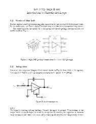
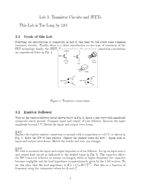
<strong>Lab</strong> 3: <strong>Trans<strong>is</strong>tor</strong> <strong>Circuits</strong> <strong>and</strong> <strong>JFETs</strong><strong>Th<strong>is</strong></strong> <strong>Lab</strong> <strong>is</strong> <strong>Too</strong> <strong>Long</strong> <strong>by</strong> <strong>50</strong>%<strong>3.1</strong> Goals of th<strong>is</strong> <strong>Lab</strong>Following our introduction to trans<strong>is</strong>tors in <strong>Lab</strong> 2, th<strong>is</strong> time we will study some commontrans<strong>is</strong>tor circuits. Finally, there <strong>is</strong> a short introduction to one type of trans<strong>is</strong>tor of theFET technology family, the JFET. For convenience, the trans<strong>is</strong>tor connection conventionsare reproduced below in Fig. 1.Figure 1: <strong>Trans<strong>is</strong>tor</strong> connections.3.2 Emitter FollowerWire up the emitter follower circuit shown below inFig.2. Inputasinewave with amplitudesymmetric about ground. Compare input <strong>and</strong> output of your follower. Increase the inputamplitude beyond 5 V. Sketch the input <strong>and</strong> output wave forms.3.2.1Replace the emitter res<strong>is</strong>tor connection to ground with a connection to ,15 V, as shown inFig. 3. Keep the 270 base res<strong>is</strong>tor. (Ignore the dashed boxes for now.) Again look atinput <strong>and</strong> output wave forms. Sketch the results <strong>and</strong> note any changes.3.2.2We w<strong>is</strong>h to measure the input <strong>and</strong> output impedances of our follower. Set up an input source<strong>and</strong> output load circuit as indicated <strong>by</strong> the dashed boxes in Fig. 3. The capacitor allowsthe DC trans<strong>is</strong>tor behavior to remain unchanged, while at higher frequency the capacitorbecomes negligible <strong>and</strong> the load impedance <strong>is</strong> approximately given <strong>by</strong> the 1 k res<strong>is</strong>tor. Tosee th<strong>is</strong> show that the load impedance <strong>is</strong> R [1 + 1=(!RC) 2 ] 1=2 . Plot th<strong>is</strong> as a function offrequency using the component values for R <strong>and</strong> C.1
+15 V2702N3904Vin3.3kVoutFigure 2: Basic emitter follower.+15 VVin10 k2N39043.3kVout+3.3 MF1 k-15 VFigure 3: Symmetric follower with input (source) <strong>and</strong> output (load) stages shown in thedashed-line boxes.2
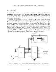
To measure Z out ,we consider the Thevenin equivalent circuit with the load, cons<strong>is</strong>ting ofthe 1 k load in parallel with the 3:3 k emitter res<strong>is</strong>tor, in series with Z out , hence formingavoltage divider. Operating at a frequency well above ! 3db of the load, measure the outputamplitude with <strong>and</strong> without the 1 k load to determine Z out .To measure Z in , remove the load. The entire follower now represents an impedance Z inin series with the 10 k source res<strong>is</strong>tor. Hence, <strong>by</strong> measuring the signal amplitude on eachside of the 10 k res<strong>is</strong>tor, we can determine Z in .<strong>Th<strong>is</strong></strong>may be dicult to measure.An important point of the emitter follower <strong>is</strong> that it represents a large input impedance<strong>and</strong> a small output impedance. The input impedance <strong>is</strong> about Z in Z load , whereas Z out Z source =, where Z load <strong>is</strong> the load to be driven <strong>by</strong> the emitter-follower including any emitterres<strong>is</strong>tor (3:3 k here), <strong>and</strong> Z source <strong>is</strong> the source impedance of the signal being delivered tothe emitter-follower. Do these expectations agree with your measurements ?3.3 Current SourceThe arrangement shown in Fig. 4 (left) can serve asanapproximate current source. Usethe 10 k variable res<strong>is</strong>tor on your prototype board as the load to be driven <strong>by</strong> the currentsource. Again, measure the collector current delivered to the load <strong>by</strong> the voltage drop acrossthe 1 k res<strong>is</strong>tor. Starting with the highest value, vary (slowly!) the load res<strong>is</strong>tance whilemeasuring the current. How good <strong>is</strong> th<strong>is</strong> current source? At whatvalue of R does thedelivered current deviate <strong>by</strong> more than 20% from the initial value?+15 V+15 V1k6.8 k(load) R0.25 MF56 kVoutVin2N3904+5 V4702N39045.6k820680Figure 4: A simple current source (left), <strong>and</strong> a common emitter amplier (right).3.4 Common-emitter AmplierSet up the common-emitter amplier shown in Fig. 4 (right). Input a small-amplitude sinewave. Measure the voltage gain of the amplier V out =V in over the frequency range <strong>50</strong> Hz to10 kHz. Make a rough plot of gain versus log 10 of frequency. What <strong>is</strong> the measured ! 3dbpoint? Does th<strong>is</strong> agree with your expectation?3
+ 15 VV in0.01 MF2N5485V out1 M 4.7 kFigure 6: Basic JFET source follower.5