Samsung SCH-210 service manual.pdf - Free
Samsung SCH-210 service manual.pdf - Free
Samsung SCH-210 service manual.pdf - Free

Create successful ePaper yourself
Turn your PDF publications into a flip-book with our unique Google optimized e-Paper software.
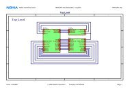
Circuit Description6-1-3 Baseband PartMOBILE SYSTEM MODEM (MSM)The MSM equipped with the INTEL 80186 CPUcore is an important component of the CDMAcellular phone. The MSM comes in a 176 pinsTQFP package. The interface block diagram isshown on page 6-3.ADC InterfaceADC_CLK (pin 3), ADC_ENABLE (pin 1) andADC_DATA (pin 2) are required to control theinternal ADC in the BBA.MICROPROCESSOR INTERFACEThe interface circuitry consists of reset circuit,address bus (A0-A19), data bus (AD0-AD15), andmemory controls (ALE, DT_R, HWR/, LWR/,RAM_CS/, ROM_CS).INPUT CLOCKCPU clock: 27 MHzTXCO/4 (pin 34): 4.92 MHz. This clock signalfrom the BBA is the reference clock for the MSMexcept in CDMA mode.CHIPX8 : 9.8304 MHz. The reference clock usedduring the CDMA mode.BBA INTERFACECDMA, FM Data InterfaceTXIQDATA0-7 (pins 24-32) : TX data bus usedduring both CDMA and FM mode.C_RX_IDATA0-3 (pins 16-20) andC_RX_QDATA0-3 (pins 12-15) : RX data busused during CDMA mode.FM_RX_IDATA (pin 7) and FM_RX_QDATA(pin 8) : RX data bus used during FM mode.Data Port InterfaceIncludes the UART. Also, supports DiagnosticMonitor (DM) and HP equipment interface.CODEC InterfaceThe MSM outputs 2.048 MHz PCM_CLK (pin 19)and 8 KHz CODEC_SYNC (pins 16,20) to theCODEC (U117). The voice PCM data from theMSM (U101) PCM_DIN (pin135) is compressedinto 8KHz by QCELP algorithm in the CDMAmode. In FM mode, the data is processed byD_FM.RF InterfaceTX : TX_AGC_ADJ (pin 35) port is used to controlthe TX power level and PA_ON (pin 44) signal isused to control the power amplifier.RX : AGC_REF (pin 36) port is used to control theRX gain and TRK_LO_ADJ (pin 45) is used tocompensate the TCXO clock.General Purpose I/O Register PinsInput/output ports to control external devices.ClockTX_CLK (pin 22), TX_CLK/(pin 23) : Analog toDigital Converter (ADC) reference clock used inTX mode.CHIPX8 : ADC reference clock used in CDMARX mode.FMCLK : Reference clock in FM RX mode.Power Down ControlWhen the IDLE/ signal turns LOW, only the TXsections will be disabled. If both the IDLE/ andSLEEP/ changes to LOW, all the pins except forthe TXCO is disabled.6-2 <strong>Samsung</strong> Electronics - Contents may change without notice.