Fast Fabrication of InP-based HBT using a Novel Coplanar Design
Fast Fabrication of InP-based HBT using a Novel Coplanar Design
Fast Fabrication of InP-based HBT using a Novel Coplanar Design

You also want an ePaper? Increase the reach of your titles
YUMPU automatically turns print PDFs into web optimized ePapers that Google loves.
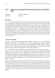
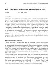
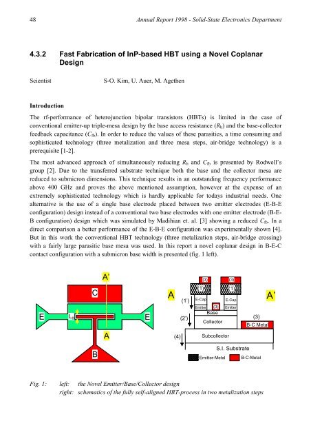
48 Annual Report 1998 - Solid-State Electronics Department4.3.2 <strong>Fast</strong> <strong>Fabrication</strong> <strong>of</strong> <strong>InP</strong>-<strong>based</strong> <strong>HBT</strong> <strong>using</strong> a <strong>Novel</strong> <strong>Coplanar</strong><strong>Design</strong>ScientistS-O. Kim, U. Auer, M. AgethenIntroductionThe rf-performance <strong>of</strong> heterojunction bipolar transistors (<strong>HBT</strong>s) is limited in the case <strong>of</strong>conventional emitter-up triple-mesa design by the base access resistance (R b ) and the base-collectorfeedback capacitance (C fb ). In order to reduce the values <strong>of</strong> these parasitics, a time consuming andsophisticated technology (three metalization and three mesa steps, air-bridge technology) is aprerequisite [1-2].The most advanced approach <strong>of</strong> simultaneously reducing R b and C fb is presented by Rodwell’sgroup [2]. Due to the transferred substrate technique both the base and the collector mesa arereduced to submicron dimensions. This technique results in an outstanding frequency performanceabove 400 GHz and proves the above mentioned assumption, however at the expense <strong>of</strong> anextremely sophisticated technology which is hardly applicable for todays industrial needs. Onealternative is the use <strong>of</strong> a single base electrode placed between two emitter electrodes (E-B-Econfiguration) design instead <strong>of</strong> a conventional two base electrodes with one emitter electrode (B-E-B configuration) design which was simulated by Madihian et. al. [3] showing a reduced C fb . In adirect comparison a better performance <strong>of</strong> the E-B-E configuration was experimentally shown [4].But in this work the conventional <strong>HBT</strong> technology (three metalization steps, air-bridge crossing)with a fairly large parasitic base mesa was used. In this report a novel coplanar design in B-E-Ccontact configuration with a submicron base width is presented (fig. 1 left).A’(3)(3)EL BCEA(1’)(2’)(1) (1)E-CapE-CapEmitter(3)BaseCollectorEmitter(3)B-C MetalA’A(4)SubcollectorBEmitter-MetalS.I. SubstrateB-C-MetalFig. 1: left: the <strong>Novel</strong> Emitter/Base/Collector designright: schematics <strong>of</strong> the fully self-aligned <strong>HBT</strong>-process in two metalization steps
Annual Report 1998 - Solid-State Electronics Department 49This approach combines low base-collector feedback capacitance, low access resistance due to thefull self-alignment and a very fast fabrication process avoiding air-bridge crossings. Base width (L B )smaller than 0.5 µm and emitter to base mesa area ratio near to 1 are possible <strong>using</strong> conventionalphotolithography. Additionally, during base and collector mesa etching the T-shaped base activearea, which is nearly completely surrounded by the emitter area, is efficiently protected.<strong>Fabrication</strong> <strong>of</strong> InGaAs/<strong>InP</strong> <strong>HBT</strong> and ResultsThe key technology step is the simultaneous and fully self-aligned evaporation <strong>of</strong> base and collectormetalization which is enabled by the new design. The metalic contacts in the active as well as in thepad area are simultaneously evaporated and the separation <strong>of</strong> active and pad areas is performed bywet chemical underetching realizing a quasi air-bridge configuration.Table 1 shows the used epitaxial layers grown on a semi-insulating <strong>InP</strong> substrate by low-pressuremetal-organic chemical vapor deposition (LP-MOCVD). Si and C are used as the n-type and p-typedopants, respectively. The p-type dopant source is carbon-tetrachlroride (CCl 4 ). Between the <strong>InP</strong>emitter and p + -InGaAs base an undoped InGaAs spacer layer (10 nm) is inserted in order to improvethe electron injection into the base. The detailed epitaxy growth process is described in reference[5]. The <strong>HBT</strong> is fabricated by optical lithography, wet chemical etching and with non-alloyedcontacts.Table 1: Epitaxial layerEmitter CapEmitterSpacerBaseCollectorSub-CollectorBufferSubstraten + -InGaAs (150 nm)n-<strong>InP</strong> (100 nm)un-InGaAs (10 nm)p + -InGaAs (150 nm)un-InGaAs (280 nm)n + -InGaAs (400 nm)un- <strong>InP</strong> (50 nm)s.i-<strong>InP</strong>The first step <strong>of</strong> the fabrication is the Ti/Pt/Au emitter metalization on the n + -InGaAs cap layer (step1 in fig. 1 right). The emitter metal is used as a mask for emitter mesa etching. H 3 PO 4 : H 2 O 2 : H 2 Oand H 3 PO 4 : HCl are used for etching <strong>of</strong> the InGaAs emitter cap layer and the <strong>InP</strong> emitter layer,respectively. The second step is base definition followed by etching to the n + -InGaAs sub-collectorlayer (step 2). The base/collector metal <strong>of</strong> Pt/Ti/Pt/Au is then evaporated in one step and lifted <strong>of</strong>f(step 3). The final step is the collector mesa isolation (step 4).Fig. 2 shows the SEM-picture <strong>of</strong> the fabricated <strong>InP</strong>/InGaAs <strong>HBT</strong> with emitter area 4 x 10 µm 2 . Thelayer stack underneath the connecting electrodes is completely removed by underetching. A verylow base finger width (L B ≤ 0.5 µm) and an almost ideal emitter/base mesa area ratio (A E /A Bmesa ≈0.9) is realized. Current gain (β) <strong>of</strong> 20 and very small <strong>of</strong>fset voltage (< 30 mV) are achieved. Theon-wafer S-parameter measurements were performed <strong>using</strong> an HP8510C network analyzer in the
50 Annual Report 1998 - Solid-State Electronics Departmentfrequency range from 45 MHz to 45 GHz. The cut<strong>of</strong>f frequency (f T ) <strong>of</strong> 100 GHz was extrapolated(slope <strong>of</strong> 20 dB/decade) at V CE <strong>of</strong> 2V and J C =8x10 4 A/cm 2 .Fig. 2:SEM-picture <strong>of</strong> fabricated <strong>InP</strong>/InGaAs <strong>HBT</strong>.In summary, we have presented a novel coplanar <strong>HBT</strong> design with inserted small area T-shapedbase contact which can realize an almost ideal emitter to base mesa area ratio <strong>of</strong> nearly 1 and smallfeed back capacitance (C fb ). The key fabrication technology step is the simultaneous and fully selfalignedevaporation <strong>of</strong> base and collector metalization. The design <strong>of</strong> two emitter contact pads resultin a direct coplanar device topology without any air-bridge crossing. A <strong>InP</strong>/InGaAs <strong>HBT</strong> with thisdesign and technology have shown promising rf-performance (f T >100 GHz). This technology showsthat high performance <strong>InP</strong>/InGaAs <strong>HBT</strong> can be produced in a cost-effective manner.References[1] Y. Matsuoka, S.Yamahata, K. Kurishima and H. Ito: "Ultrahigh-Speed <strong>InP</strong>/InGaAs Double-Heterostructure Bipolar Transistors and Analyses <strong>of</strong> Their Operation", Jpn. J. Appl. Phys.,1996, 35 pp. 5646-5654[2] Q. Lee, B. Agarwal, D. Mensa, R. Pullela, J. Guthrie, L. Samoska and M. J. W. Rodwell:"A > 400 GHz fmax Transferred-Substrate Heterojunction Bipolar Transistor IC Technology"IEEE Electron Device Lett., 1998, 19 pp. 77-79[3] M. Madihian, K. Honjo, H. Toyoshima, and S. Kumashiro: "The <strong>Design</strong>, <strong>Fabrication</strong>, andCharacterization <strong>of</strong> a <strong>Novel</strong> Electrode Structure Self-Aligned <strong>HBT</strong> with a Cut<strong>of</strong>f Frequency <strong>of</strong>45 GHz", IEEE Tran. Electron Devices, 1987, ED-34, pp. 1419-1428[4] W. U. Liu, D. Costa, and J. Harris: "<strong>Novel</strong> Doubly Self-Aligned AlGaAs/GaAs <strong>HBT</strong>",Electronics Letters, 1990, 26, pp. 1361-1362[5] A. Lindner, P. Velling, W. Prost, A. Wiersch, E. Kuphal, A. Burchard, R. Margerle,M. Deicher, F.J. Tegude: "The Role <strong>of</strong> Hydrogen in Low-Temperature MOVPE Growth andCarbon Doping <strong>of</strong> In 0.53 Ga 0.47 As for <strong>InP</strong>-<strong>based</strong> <strong>HBT</strong>“, J. Crystal Growth, 1997, 170 pp. 287-291.