ims chips
ims chips
ims chips
- No tags were found...

Create successful ePaper yourself
Turn your PDF publications into a flip-book with our unique Google optimized e-Paper software.
HistoryFounded by the state of Baden-Württemberg in 1983 in response to the“Japanese challenge“ in MicroelectronicsToday´s figures94 employees14.7 million Euros budget volume14 publicly funded joint projectsMore than 100 individual cooperation with companies, research facilities and universities(as of 4/2010)3 IMS Overview 2010© IMS 2009
Milestones1983 Foundation1986 Operational start-up of the cleanroom1987 3 µm CMOS1990 2 µm Gate-Forest ®1992 HDRC ® image sensors1993 ISO 9001 / CECC1996 0.8 µm mixed signal GATE-FOREST ®1997 Stencil masks2000 Vistec Ebeam writer SB-3522003 Marketing HDRC ® image sensors2006 Chipfilm-technology2008 0.5 µm GATE-FOREST ®4 IMS Overview 2010© IMS 2009
IMS Association of SponsorsNetwork of IMS key account clients• Opportunity to co-decide IMS development und direction (6 of 25 board members)• Support in front end research and educational programs• Memberships for companies, associations and individualsVerein der Förderer des Instituts für Mikroelektronik Stuttgart e.V.5 IMS Overview 2010© IMS 2009
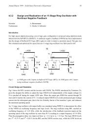
IMS DivisionsASICsVisionSi Technology6 IMS Overview 2010Nanostructuring© IMS 2009
ASICs – Areas of OperationASICsVisionSi Technology7 IMS Overview 2010Nanostructuring© IMS 2009
ASICs – Areas of Operation• Microelectronic systems• ASIC small seriesASICs• Support for small and medium-scale companies in design ofmicroelectronics systems, feasibility studies, expertises, FPGAmigration, prototype developments, preproduction samples.• Development, qualification and serial deliveries ofdigital/analog/mixed-signal ASICs of 100 – 100,000 units.8 IMS Overview 2010© IMS 2009
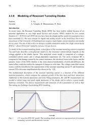
ASICs - ExamplesGATE FOREST ® ASICs Full-Custom Chips 24 V GATE FOREST ®• Digital and analog functions• 100 to 250 k gate• ChipFilm variations inthe pipeline• Integrated sensors• High-voltagetransistors for 200 V• Photodiode lines• Combination process3/5 V + 24 V• Power transistors9 IMS Overview 2010© IMS 2009
ASICs - ApplicationsMarine diesel fuel with IMS ASICBraille module with IMS ASICsTerraSAR-X with IMS ASICsRetina implant with IMS sensorchip10 IMS Overview 2010© IMS 2009
Si Technology DivisionSi TechnologyASICsNanostructuring11 IMS Overview 2010Vision© IMS 2009
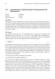
Si Technology Division• Silicon Processing• Development of ultra-thin <strong>chips</strong>• Add-on processingSi Technology• 750 m 2 class 1-10 cleanroom (with an additional 450 m 2 in construction)• Manufacture of integrated circuits on 6 inch wafers, 0.5 and 0.8 µm CMOSprocessing, chip assembly for ceramic packaging, COB and bare dies• Individual processing, wafer processing, Add-on processing12 IMS Overview 2010© IMS 2009
Si Technology: ExamplesThin flexible chipComparsion of bulk and Chipfilm diesMicromechanicsSi pellet, Avogadro project (PTB)13 IMS Overview 2010© IMS 2009
Si Technology: PartnersMicroelectronic suppliersSupplier of standardsSemiconductor manufacturersHardware and componentmanufacturersResearch facilitiesSeminconductor hardware manufacturersMicromechanics user and manufacturers14 IMS Overview 2010© IMS 2009
Nanostructuring DivisionNanostructuringSi TechnologyVision15 IMS Overview 2010ASICs© IMS 2009
Nanostructuring Division• Photomasks• M(E)MS• Diffractive Optical Elements• Nano DiesNanostructuring• Powerful E-Beam-Writer• Development und manufacture of state-of-the-art photomasks anddiffractive optical components• Process development, evaluation of new materials and processes• Structuring in nanometers, highly-precise measurements16 IMS Overview 2010© IMS 2009
NanostructuringCenter for nanostructure prototypingE-BEAM WriterVistec SB352WAFER MANUFACTUREHamaTech ModuTrackCMOS InfrastructureSTS PegasusMASK PRODUCTIONHamaTech ASR5000 coaterHamaTech ASP5000 developerPlasmatherm mask etcher GenIII/IVVistec LMS IPRO IIVistec CD-SEM LWM900017 IMS Overview 2010© IMS 2009
Nanostructuring: ProductsDirect writingCMOS personalizationNano componentsDiffractive optical elementsReplication master (Qz(Qz, , Si)MEMSMembranesCMOS & MEMSMasksEUV masksBinary masksPSMServiceEvaluation of tools, materials,Process development18 IMS Overview 2010© IMS 2009
Nanostructuring: Partnersresist evaluationadvanced masksoptical componentsdirect writeimprint templatespattern generator,CD-SEM, placementtool evaluationmulti Beam lithography19 IMS Overview 2010© IMS 2009
Vision Division (Image Sensors)VisionNanostructuringASICs20 IMS Overview 2010Si Technology© IMS 2009
Vision Division (Image Sensors)• Imaging sensors and actorics• CMOS image sensors (HDRC © )• Camera and systems technologyVision• Research and development of new image sensortechnologies• Development and manufacture of highly-dynamic customizedCMOS image sensors• Specially developed sensors for biomedical applications• Development of reference systems incl. optics, packaging,circuit design, image processing und sytems integration21 IMS Overview 2010© IMS 2009
Vision: ApplicationsINDUSTRIAL IMAGE PROCESSINGHighly-dynamic HDRC ® image sensors forextreme illumination conditionsMEDICAL TECHNOLOGYMiniature image sensors for endoscopes andretina implants for the vision impairedAIR AND SPACERadiation resistant sensor design andproduction technology for the application inspaceAUTOMOBILEImage sensors for traffic technology inautomotive conditions22 IMS Overview 2010© IMS 2009
Vision: ProductsHDRC ® - IMAGE SENSOR FOR PILZThe HDRC ® image sensor developed at theIMS is an essential component of therevolutionary SafetyEYE ® system of theOstfildern-based Pilz GmbH & Co. KGcompanyHDRC ® QUOTIENTEN-PYROMETERThe HDRC ® Q-PyroCam enablesnon-contact measuring of hightemperatures23 IMS Overview 2010© IMS 2009
Education at the IMSUniversity of StuttgartThe Institut für Nano- und Mikroelektronische Systeme (INES) offers lecturesas well as diploma thesis and student research program opportunitiesStudent research and diploma thesis programs are possible at the facultyelectrical and production engineeringMicroelectronic Technology Seminar- At the Technischen Akademie Esslingen (TAE)- On demand for companiesSMC – Practical Course for StudentsTwo-week summer course24 IMS Overview 2010© IMS 2009
IMS CHIPSRingsensorABBILDAirport SystemIPLNanoimprintTerraSAR-XHDRC ® PyroCamSOHARRetinaMoDektChipfilmSensorzeileNIRWARNSafety Eye ®IVP KapselAPS SternsensorMini-EndoskopHyperBrailleGateForest ®MORESMCIVP SensorMikrohandhabungMulti-BeamVIPcontact:info@<strong>ims</strong>-<strong>chips</strong>.dewww.<strong>ims</strong>-<strong>chips</strong>.de25 IMS Overview 2010© IMS 2009