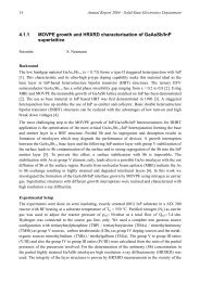
radiation effects in semiconductor materials and devices for space
radiation effects in semiconductor materials and devices for space
radiation effects in semiconductor materials and devices for space

You also want an ePaper? Increase the reach of your titles
YUMPU automatically turns print PDFs into web optimized ePapers that Google loves.
RADIATION EFFECTS INSEMICONDUCTOR MATERIALSAND DEVICES FOR SPACEAPPLICATIONSCor Claeys <strong>and</strong> Eddy Simoen© IMEC 2010
OUTLINEIntroductionTotal Dose Effects <strong>in</strong> th<strong>in</strong> gate oxidesRILC, RSB, SEGR, Latent DamageMicrodose EffectsDevice Scal<strong>in</strong>g▸ Bulk & SOI F<strong>in</strong>FETs▸ Ge <strong>devices</strong>Conclusions© IMEC 2010 IEEE EDS Colloquia, June 7 / C. Claeys 2
INTRODUCTIONCOTS important <strong>for</strong> Space ApplicationsAdvanced CMOS TechnologiesReduced Gate DielectricsAlternative Substrates: SOI, sSOI, Ge, sGe, GOI...Advanced Process Modules:High-κ Dielectrics, Stra<strong>in</strong> Eng<strong>in</strong>eer<strong>in</strong>g, …Alternative Device ConceptsDouble gate, F<strong>in</strong>FETs, GAA, Nanowires, …Impact on Radiation Harden<strong>in</strong>g ?© IMEC 2010 IEEE EDS Colloquia, June 7 / C. Claeys 3
IONIZING AND DISPLACEMENTDAMAGE = F(PARTICLE, ENERGY)The energy loss rate throughionization <strong>and</strong> excitation ofthe Si lattice (LET) <strong>and</strong> throughatomic displacements (NIEL)versus proton energy. Only afraction of 1% of the energyloss goes <strong>in</strong>to displacementprocesses© IMEC 2010 IEEE EDS Colloquia, June 7 / C. Claeys 5
IONIZING DAMAGE IN MOSGate: carries away the chargeOxidegate++n-Si--+p-type siliconSilicon: electron-hole pairs canrecomb<strong>in</strong>e <strong>in</strong> the neutral bulkIn case of a p-n junction, theelectric field separates electrons<strong>and</strong> holes. This leads to atransient charg<strong>in</strong>g phenomenonS<strong>in</strong>gle Event Upsets (SEU)Permanent ioniz<strong>in</strong>g damage only<strong>in</strong> the dielectric layers: gate oxide,isolation or field oxide <strong>and</strong> buriedoxide (SOI)© IMEC 2010 IEEE EDS Colloquia, June 7 / C. Claeys 6
STANDARD TOTAL DOSE RADIATIONEFFECTSN ot & N it© IMEC 2010 IEEE EDS Colloquia, June 7 / C. Claeys 7
GATE OXIDE SCALINGGate current be<strong>for</strong>e (full l<strong>in</strong>es) <strong>and</strong> after (dashed l<strong>in</strong>es) a 67 MeV 2.9x10 12 p/cm 2proton ir<strong>radiation</strong> <strong>for</strong> a 0.09 µm n- <strong>and</strong> 0.08 µm p-MOSFET with 2.0 nm oxide.10 -9 -1.5 -1 -0.5 0 0.5 1 1.5Gate Current (A)10 -1010 -1110 -12L=0.09 µm n-MOS; L=0.08 µm p-MOSV DS=-0.025 Vn-MOSp-MOSfloat<strong>in</strong>gV DS=0.025 Vn-MOSp-MOS10 -13t ox=2 nmGate Voltage (V)© IMEC 2010 IEEE EDS Colloquia, June 7 / C. Claeys 8
DEVICE SCALING∆V t ~ t ox2Good TID resistance of the Gate oxideRadiation <strong>effects</strong> will be caused by parasitic conductionrelated toShallow Trench Isolation oxide: BulkBuried oxide <strong>for</strong> SOI <strong>devices</strong>Occurrence of other <strong>radiation</strong> related phenomena© IMEC 2010 IEEE EDS Colloquia, June 7 / C. Claeys 9
IONIZING DAMAGE: THIN GATE OXIDESUni<strong>for</strong>m gate current flowBreakdown pathTrap-assisted RILCRILC by <strong>radiation</strong>-<strong>in</strong>ducedNeutral electron traps© IMEC 2010 IEEE EDS Colloquia, June 7 / C. Claeys 10
IMPACT OF HIGH-ENERGY IONS ON GATEOXIDERadiation-Induced Leakage Current(RILC)Radiation-Induced Soft Breakdown(RSB)Increase of off-state power consumptionbut no real concern© IMEC 2010 IEEE EDS Colloquia, June 7 / C. Claeys 11
ION-INDUCED DEGRADATION OF GATEDIELECTRICSA. Cester, L. B<strong>and</strong>iera, M. Ceschia, G. Ghid<strong>in</strong>i <strong>and</strong> A. Paccagnella, IEEE Trans. Nucl. Sci.,48, pp. 2093-2100 (2001)© IMEC 2010 IEEE EDS Colloquia, June 7 / C. Claeys 12
SINGLE EVENT GATE RUPTUREL.W. Massengill, B.K. Choi, D.M. Fleetwood, R.D. Schrimpf, M.R. Shaneyfelt, T.L. Meisenheimer,P.E. Dodd, J.R. Schwank, Y.M. Lee, R.S. Johnson <strong>and</strong> G. Lucovsky, IEEE Trans. Nucl. Sci., 48,pp. 1904-1912 (2001)SEGR* Operat<strong>in</strong>g voltagelower than criticalvalue* Critical LET threshold© IMEC 2010 IEEE EDS Colloquia, June 7 / C. Claeys 13
LATENT RADIATION DAMAGE IN THIN GATEOXIDES1J.S. Suehle, E.M. Vogel, P. Roitman, J.F. Conley Jr., J.B. Bernste<strong>in</strong> <strong>and</strong> C.E. We<strong>in</strong>traub,Appl. Phys. Lett., 80, pp. 1282-1284 (2002)129 Xe Ir<strong>radiation</strong>, t ox= 3.0 nm, V stress= - 4.9 V* No parameter shiftafter ir<strong>radiation</strong> only* Reduced oxide lifetimeafter accelerated test<strong>in</strong>gln(ln(1/(1-F)))0-1-2-31 10 100 1000 10000Pre-ir<strong>radiation</strong>1 x 10 5 ions/cm 21 x 10 6 ions/cm 21 x 10 7 ions/cm 2LET > 30 MeV/cm 2Time-to-Breakdown (s)Weibull lifetime distribution of MOS capacitors subjected to constant voltage stressat V stress =-4.9 V be<strong>for</strong>e <strong>and</strong> after heavy ion ir<strong>radiation</strong>© IMEC 2010 IEEE EDS Colloquia, June 7 / C. Claeys14
LATENT RADIATION DAMAGE IN THIN GATEOXIDESJ.S. Suehle, E.M. Vogel, P. Roitman, J.F. Conley Jr., J.B. Bernste<strong>in</strong> <strong>and</strong> C.E. We<strong>in</strong>traub,Appl. Phys. Lett., 80, pp. 1282-1284 (2002)Weibull lifetime distribution of MOS capacitors subjected to constant voltage stressat V stress =-5.0 V be<strong>for</strong>e <strong>and</strong> after 60 Co ir<strong>radiation</strong>.© IMEC 2010 IEEE EDS Colloquia, June 7 / C. Claeys 15
LATENT RADIATION DAMAGE - ION FLUENCEEFFECTA. Cester, S. Cim<strong>in</strong>o, E. Mir<strong>and</strong>a, A. C<strong>and</strong>elori, G. Ghid<strong>in</strong>i <strong>and</strong> A. Paccagnella, IEEE Trans. Nucl. Sci., 50,pp. 2167 2175 (2003)Gate current dur<strong>in</strong>g CVS at V CVS = 4.2 V on threesamples with gate area 10 -2 cm 2 irradiated with256-MeV I ions at different fluencesExcess gate current Density (J e )normalized to the ion fluence (φ)measured dur<strong>in</strong>g CVS at V CVS =4.2 V© IMEC 2010 IEEE EDS Colloquia, June 7 / C. Claeys 16
LATENT RADIATION DAMAGE – STRESSINGVOLTAGEA. Cester, S. Cim<strong>in</strong>o, E. Mir<strong>and</strong>a, A. C<strong>and</strong>elori, G. Ghid<strong>in</strong>i <strong>and</strong> A. Paccagnella, IEEE Trans. Nucl. Sci., 50,pp. 2167-2175 (2003)=∆I N [1-exp(-λt s )]Gate current derivative dI g /dt of the gate current, equivalent to the density of spots, withrespect to the stress<strong>in</strong>g time dur<strong>in</strong>g CVS. The derivative has been evaluated as the slope of the<strong>in</strong>itial part of the gate current evolution (t stress < 1000 s), i.e., where the gate current<strong>in</strong>creases almost l<strong>in</strong>early© IMEC 2010 IEEE EDS Colloquia, June 7 / C. Claeys 17
100 NM PD SOI TECHNOLOGY10-20% CHANGE F(ION FLUENCE)STAIRCASE VOLTAGE STRESSA. Cester, S. Gerard<strong>in</strong>, A. Paccagnella, E. Simoen <strong>and</strong> C. Claeys, IEEE Trans. Nucl. Sci., 52, pp. 2252-2258 (2005)Gate current measured at V g = V g,stress dur<strong>in</strong>g FN <strong>in</strong>jection of <strong>devices</strong> processed <strong>in</strong> an 0.1 µm PDSOI technology. V g,stress starts from 2.5 V <strong>and</strong> <strong>in</strong>creases up to 4 V with 50-mV step every 100 s.The stress was per<strong>for</strong>med on fresh <strong>and</strong> irradiated <strong>devices</strong> with two different ion fluences(2.5 <strong>and</strong> 0.5 I ions/µm 2 ).© IMEC 2010 IEEE EDS Colloquia, June 7 / C. Claeys 18
65 NM FD SOI TECHNOLOGYNO CHANGE.A. Griffoni, S. Gerard<strong>in</strong>, A. Cester, A. Paccagnella, E. Simoen <strong>and</strong> C. Claeys, IEEE Trans. Nucl. Sci., 54,pp. 2257-2263 (2007)Gate current time to breakdown <strong>for</strong> irradiated (2.5 I ions/µm 2 ) <strong>and</strong> unirradiated FD SOI MOSFETs(W=L = 10 µm/10 µm) fabricated <strong>in</strong> a 65 nm technology with different stra<strong>in</strong> levels.The <strong>devices</strong> were stressed with a staircase voltage from 2 V to 4 V with 50-mV steps, each last<strong>in</strong>g100 s.© IMEC 2010 IEEE EDS Colloquia, June 7 / C. Claeys 19
HEAVY ION STRIKES: MICRODOSE EFFECTSS. Gerard<strong>in</strong>, M. Bagat<strong>in</strong>, A. Cester, A. Paccagnella <strong>and</strong> B. Kaczer, IEEE Trans. Nucl. Sci., 53, pp. 3675-3680 (2006)charge build-up <strong>in</strong> the STIcharge build-up <strong>in</strong> the LDD regionStatistical <strong>in</strong> natureDefect generation <strong>in</strong> the oxide© IMEC 2010 IEEE EDS Colloquia, June 7 / C. Claeys 20
TRANSISTOR SCALINGNew process modulesNew <strong>materials</strong>New device conceptsmetal gateF<strong>in</strong>FETgraphenenanowiresGe/IIIV16 <strong>and</strong> beyondsilicide>=130USJstra<strong>in</strong>90-65-45NiSi NiSiFUSIStra<strong>in</strong>, USJ25 nmHfO 2high -ktime45-32High-k, Metal Gate32-22-16Non-planar<strong>devices</strong>Front End© IMEC 2010 IEEE EDS Colloquia, June 7 / C. Claeys 21
HIGH MOBILITY SUBSTRATESGe DEVICESR. Arora, E. Simoen, E.X. Zhang, D.M. Fleetwood, R.D. Schrimpf,K.F. Galloway, B.K. Choi,J. Mitard, M. Meuris, C. Claeys, A. Madan,J. D. Cressler, RADECS 2009 (IEEE T-NS)8 ML SI 5 ML SI© IMEC 2010 IEEE EDS Colloquia, June 7 / C. Claeys 23
CONCLUSIONS‣ Deep submicron CMOS technologies are <strong>radiation</strong> hard <strong>for</strong> total dose <strong>effects</strong>‣STI or BOX must be optimized‣ RILC, RSB, SEGR <strong>and</strong> Latent Damage‣For th<strong>in</strong> gate oxides heavy ion strikes are important‣ Microdose <strong>effects</strong> have to be taken <strong>in</strong>to account requir<strong>in</strong>g a statistical analysis of atechnology‣New process modules, new <strong>materials</strong> <strong>and</strong> alternative device concepts have to be<strong>in</strong>vestigated© IMEC 2010 IEEE EDS Colloquia, June 7 / C. Claeys 24
ACKNOWLEDGMENTThe authors want to acknowledgeA. Griffoni, D. Fleetwood, K. Galloway,S. Gerard<strong>in</strong>, G. Meneghesso, A. Paccagnella <strong>and</strong> S. Put<strong>for</strong> the use of co-authored results.Part of the work was done under ESA contract22485/09/NL/PA.The imec Process Technology Unit is acknowledged <strong>for</strong> thedevice fabrication© IMEC 2010 IEEE EDS Colloquia, June 7 / C. Claeys 25
© IMEC 2010