High Voltage Microwave Devices: An Overview - CS Mantech
High Voltage Microwave Devices: An Overview - CS Mantech
High Voltage Microwave Devices: An Overview - CS Mantech

Create successful ePaper yourself
Turn your PDF publications into a flip-book with our unique Google optimized e-Paper software.
<strong>High</strong> <strong>Voltage</strong> <strong>Microwave</strong> <strong>Devices</strong>: <strong>An</strong> <strong>Overview</strong>D. Miller and M. DrinkwineM/A-COM, Inc. <strong>Microwave</strong> Solutions Business Unit5310 Valley Park Drive, Roanoke, VA 24019Phone: 540 563-8600, E-mail: millerd@tycoelectronics.comAbstractEmerging technologies like SiC and GaN offer the potentialfor manufacturable high performance microwave powerdevices operating at higher voltages than traditional GaAsbaseddevices. Developers of these new high-voltage-devicetechnologies are targeting applications like cell phone basestationamplifiers, SAT-COM power amplifiers, and highpower phased-array radar systems where very high power isdesirable and higher supply voltages are readily available.After defining appropriate figures of merit (FOMs) that areuseful for comparing different high voltage transistortechnologies, we present a summary of the competingtechnologies and fabrication technology overviews. Wecompare performance and “in production” cost withtraditional GaAs-based and silicon-based technologies.Examples of recently-published results are presented, includingrecent work representing higher-voltage GaAs-basedtechnologies.INTRODUCTIONToday, there are requirements for solid state microwavepower amplifiers in a wide variety of applications as shownin Figure 1 [1], including both military and commercialapplications with frequencies ranging from S-band to W-band and power levels from 0.1 W to more than 1000 W. Incontrast to the extremely high volume low cost requirementsof handheld consumer applications (for example, cellularphone power amplifiers) where low voltage operation is arequirement, these applications occur in base stations,ground stations, or large systems where much highervoltages are readily available. There are many potentialbenefits at the system level from using a higher voltage forthe power amplifier, including reduced size (if the devicepower density is increased at higher voltage, which isusually the case) and the resulting lower cost. In largesystems, power distribution may be greatly simplified byusing higher voltage and lower current to deliver the samepower. There may also be some gains in the systemefficiency from the elimination of dc-to-dc converters. Also,matching and combining may be feasible at higher outputpower levels because of the higher input and outputimpedance levels of smaller devices with higher powerdensity [1].Figure 1. Applications for GaN HEMTs (from [1]Copyright 2002 IEEE. Used by permission.)Solid state microwave power devices have been GaAsbasedor InP-based in the past, but these devices are nowbeing challenged by devices fabricated on wider bandgapmaterials which promise higher voltage operation and higherpower density. In this paper, we will review the figures-ofmerit(FOMs) useful for comparing microwave powerdevices and present a brief summary of each competingtechnology. We will conclude by comparing theirperformances and try to answer the question “Can GaAscompete?”FIGURES OF MERITThe first differentiator for comparing microwave powertransistor technologies is their useful frequency range. Thisis generally characterized by small-signal measurements ofscattering (S) parameters using a network analyzer. Onefigure-of-merit is F T , the frequency where the device’s shortcircuit current gain falls to unity. A second figure of merit isF MAX , the frequency where G MAX , the maximum availablegain (MAG) or maximum stable gain (MSG) has fallen tounity. Note that G MAX calculates the maximum gain whichcan be obtained from the device with any input and outputmatching network—since things besides gain must beconsidered when designing a power amplifier, a device maynot actually be useful all the way to F MAX .
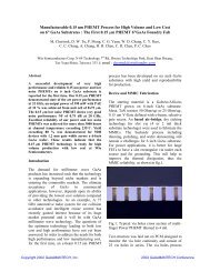
For a power amplifier, small-signal gain is not sufficient;gain at power (“associated gain”) is required. At a particularinput power level, the following definitions of associatedgain (G), drain efficiency (DE) and power-added efficiency(PAE) apply:PoutG =PPDE =PinoutDC( Pout− Pin)PAE =PDC⎞⎜⎛ 1= DE ⋅ 1 − ⎟⎝ G ⎠Figure 2 shows single device output power levels vs.frequency for various technologies.Figure 2. Average RF output power versus frequencyfor various electronic devices [2]. Copyright 2002 IEEE.Used by permission.Both solid state and vacuum tube sources are shown. Points1-5 represent “state-of-the-art” solid state deviceperformance—it is interesting to note that they fallapproximately on a straight line on this log-log plot. We canthus define “power state-of-the-art”:PSOA=fas a figure of merit for a discrete device output power valueat a particular frequency. If PSOA is greater than 1, theresult can be considered “better” than state-of-the-art, eventhough the frequency may be different than previous results.In order to compare devices which have different powersand efficiencies, we must understand the tradeoff betweenpower and efficiency that is acceptable at the system level.Figure 3 shows how two identical power amplifiers with unitoutput power of Po and PAE can be combined into a higherpoweramplifier.3⋅ P4 ⋅1052Figure 3. Two unit amplifiers with performance (Po,PAE) are combined—because of loss in the combiner, the“big amp” has lower efficiency than the unit amps.If the combiner loss is non-zero (as any real-worldcombiner must be), the “big amp” performance is:BPo = 2 ⋅ Po ⋅ (1 −1010) < 2 ⋅ PoBPoBPAE =< PAE2 ⋅ Po / PAEThis performance, higher power and lower PAE, is acceptedby the designer of the system as “equivalent” to theperformance of the unit amplifier. This tradeoff of powerand efficiency can be generalized and used to comparedevices with different output powers and efficiencies. Usingfractional 2N-way combining to achieve a 1 watt outputpower level and solving for N gives−13N =⋅ P +10 ⋅ Log(2)− LLLog(2)−10− N ⋅L10PAE1= PAE ⋅10where L is the 2-way combiner loss in dB, P the smalldevice output power in dBm, PAE the small device poweraddedefficiency, and PAE1 the combined figure of merit,PAE at a 1 watt output power level. PAE1 allows us tocompare device results which differ in both power andefficiency on a fair basis.<strong>An</strong>other FOM is cost. Ultimately, it is the system costthat is important. Therefore, when evaluating andcomparing device or IC costs, the full cost impact of aparticular implementation becomes important and manyfactors can be relevant in determining best cost for the enduser. For example, despite higher cost-per-mm 2 , a GaNimplementation for base station power amplifiers mightprove competitive with Si LDMOS if advantages of higherpower density, improved efficiency and linearity, and highertemperature operation can produce a lower systemimplementation cost. Such comparative cost evaluations gobeyond the scope of this paper; however, we will touch uponsome to the factors relevant to technology cost and provideL
estimates for $/W (=$/mm 2 /(W/mm 2 )) for comparison ofdiscrete device implementations. For SiC and GaNtechnologies, using a “now” cost comparison is not veryuseful due to immaturity of the technology and the lack ofproduction activity; therefore, reasonable expectations fortechnology and manufacturing cost-related improvementshave been applied to the values shown in Table 2. Examplesof assumptions applied to our evaluation include: 1) SiCwafers are incredibly expensive today, available only in 2”diameter, with high defect density (poor FET yields); for thistechnology to become competitively viable it is reasonableto expect, as a minimum, 3” wafers with low defect densityat costs comparable or below that of 2” SiC wafers today; 2)Si LDMOS technology has a production volume advantagevia leveraging by high-volume products (e.g. CMOS)running in the same fab; therefore, near term projections ofreasonable volume-leverage for other technologies havebeen applied to process costs.The last FOM discussed here is reliability. Requirementsfor reliability are driven by the end product. <strong>Devices</strong> goinginto “disposable” cell phones may need only a 1-2 yearlifetime, while devices going into space applications must beproven to last 20 years or even longer. For the newertechnologies in development, reliability problems arerecognized (e.g., drain current collapse), but only recentlyhave they been getting much attention for corrective action.Consequently, we have only made very rough comparativeassessments for reliability, as indicated later in Table 2.TECHNOLOGIESSi LDMOS fabrication is typically done on P+ Si waferswith a lightly doped p-type epi layer. Multiple ionimplantationsare performed—typically 3 n-type and 3 p-type implants. Gates are fabricated with WSi or CoSi onpolysilicon. <strong>High</strong> thermal cycles include HiPOX fieldoxide, thermal gate oxide, and channel/PHV/LDD drive(s).PtSi ohmic contacts are used, with a TiW barrier if Au is tobe used. The processing is similar to Si CMOS with theaddition of thick interconnect metallization for highercurrent capacity. Minimum feature sizes are generally 0.5um or larger.GaAs MESFETs use bulk GaAs wafers as substrateswhich are readily available at low cost in both 4” and 6”sizes. Doping is done with ion implantation for both n-type(Si) and p-type (Mg or Be) doping. <strong>Devices</strong> are fabricatedby doing a wet recess and lift-off of a Ti/Au gate or byselective implanting of contact regions with a refractorymetal gate. Passivation is accomplished with SiN depositedby plasma-enhanced CVD. Alloyed Ni/Au/Ge metallizationis commonly used to form n-type ohmic contacts. Theprocess is relatively simple, using 4-5 mask layers to formdiscrete devices and 10 or more for MMICs which includeMIM capacitors, thin-film resistors, and several layers ofinterconnect metallization.GaAs PHEMTs are fabricated in a very similar way toGaAs MESFETs, except the starting material has epitaxiallayers on it. Many commercial suppliers are available usingMBE or MOCVD for the epitaxial growth. Formation ofNi/Au/Ge n-type ohmic contacts is often the first step inPHEMT fabrication. <strong>Devices</strong> are isolated using ionimplantationdamage or mesa etching. Gate fabrication istraditionally done by electron-beam lithography, althoughadvances in optical lithography have made it feasible forlonger gate-length devices. Many power devices use adouble recess. Improvements in manufacturability havebeen obtained by using an etch stop layer to control thedepth of one or both recesses, which are typically wetetched. After gate liftoff using Ti/Pt/Au or Ti/Pd/Au,devices are passivated with PECVD SiN.GaN HEMTs are attractive for high-voltage operationdue to the high breakdown field of GaN. GaN HEMTstructures can be grown on SiC, sapphire, or siliconsubstrates. Use of SiC substrates, now becoming availablein 3” diameter, generally results in the best quality epi. SiCalso has very high thermal conductivity which helpsfacilitate high-power-density operation. However, SiCsubstrates are very expensive, have high defect densities,and there is only one viable vendor at present. Usually, GaNHEMTs are not intentionally doped, instead, they takeadvantage of the high sheet-charge density (1E13 cm -2 )which occurs at the AlGaN/GaN interface because ofpolarization effects [2]. Device fabrication is similar to thatfor GaAs PHEMTs using a similar number of maskinglayers to produce a discrete HEMT or IC; processingdifferences are dictated primarily by the AlGaN/GaNmaterials characteristics. Lack of suitable wet etches forAlGaN/GaN results in use of dry etching for mesa isolation.Recess etching is avoided. The high mobility of GaN allowsit to be used at millimeter-wave frequencies; therefore gatelength and lithography technique is dictated by theapplication frequency. Ohmic contacts are alloyed at around900 °C using a Ti/Al/Au metal stack which produces an“advancing interface tunneling contact”. Ni provides ahigher barrier height than Ti, so Ni is used for the gateSchottky contact. Although the essential device fabricationprocesses have been developed to produce GaN HEMTs andICs, much effort is being directed at developing moremanufacturable and reproducible processes. Also,significant activity is being directed at passivation and epigrowth for improving reliability, with emphasis on reducingdrain current collapse.SiC MESFETs are also “naturals” for high-voltageoperation by virtue of silicon-carbide’s high-fieldbreakdown. Although the fabrication technology is moremature than that for GaN HEMTs, SiC MESFETs face
similar challenges due to the high cost of SiC substratesalong with defects and/or passivation issues that give rise tocurrent instability and frequency dispersion. The lowelectron mobility of SiC, despite high saturation velocity,places limitations on use at high frequencies. For devicefabrication, n-type SiC, doped to ~3E17 cm -2 , is grown asthe channel layer and phosphorus is ion implanted to formn+ regions for ohmic contacts. Dry etching with Cl 2 is usedfor mesa isolation and, if desired, for recess etching toachieve higher breakdown voltage, but with lower Imax.Ohmic contacts are made with Ni, and alloyed at around1000 °C. Optical or e-beam lithography is used for gatedefinition with evaporated Ni/Pt/Au to form the gates.PECVD SiN is used for passivation. For X-bandfrequencies, back side via etching is done to form lowinductancesource connections, but the aggressive chemistryused is not easily stopped by the front-side metal – a processcontrol issue that also applies to GaN devices on SiC. Bycomparison with other devices described here, SiCMESFETs have high knee voltage, high pinch-off voltage,and lower Gm.Table 1. Discrete power device performance comparisonTechnologyRef Size(mm)F Vdd Gain(GHz) (V) (dB)Pout(dBm)PAE(%)Pout(W/mm)GaAs MESFET [3] 0.63 14 10 8 27 60 0.8GaAs PHEMT [4] 0.8 10 9 11 28 55 0.8Si LDMOS [5] 3 2 26 16.8 32.8 46 0.6SiC MESFET [6] 0.25 3.5 50 11.1 31.1 63 5.2GaN HEMT [6] 0.5 3.5 90 11 36.7 34 9.4HV GaAs MESFET [7] 0.48 3 25 12 29.4 54 1.8HV GaAs PHEMT [8] 0.3 1.9 12 22.8 27.8 74 2.0Table 2. Discrete power device reliability and chip costcomparison. A common value for gate-periphery-perunit-device-areais used for all technologies.TechnologyWaferRel.Size(2003)(mm)WaferCost($)ProcessCost ($)Discrete$/WGaAs MESFET high 100 150 3000 0.07GaAs PHEMT high 100 500 5000 0.13Si LDMOS high 125 100 1000 0.02SiC MESFET low 75 3000 4000 0.05GaN HEMT low 75 3000 5000 0.03HV GaAs MESFET med 100 150 3000 0.03HV GaAs PHEMT med 100 500 5000 0.05SUMMARYTable 1 shows discrete device performance results fromfoundry documentation (GaAs MESFET and PHEMT) orpublications. As shown, the wide bandgap discretes showextremely high power densities. Table 2 shows estimates offabrication cost in production. Both tables also show some“second generation” GaAs MESFET and PHEMT resultswhich narrow the performance gap significantly, whilelowering the cost to be more comparable to Si LDMOS.Table 3 compares actual product results (GaAs MESFETand PHEMT and Si LDMOS) and published large device orMMIC results (SiC and GaN). Note that the achieved powerdensities and cost per watt are quite different than thediscrete results in Table 2. It is interesting to note that theLDMOS efficiency figure-of-merit results are quite good.Table 3. Product comparison.Technology RefF Pout Gain(GHz) (W) (dB)PAE(%)Vdd(V)FETsize(mm)Cost($)PSOA W/mm n1W PAE1(%)GaAs MESFET [9] 11 12.5 22 32 10 146 0.52 -4.0 40.2 11.68GaAs PHEMT [10] 17 2 32 32 7 0.05 -1.1 34.1Si LDMOS [11] 1.8 30 14 48 26 83 56 0.01 0.36 -5.4 65.3 1.87SiC MESFET [6] 3.5 36.3 6.5 21 55 12 0.14 3.03 -5.7 28.5GaN HEMT [6] 10 38 8 29 37 12 3.61 3.17 -5.7 40.3CONCLUSIONSAmazingly high power densities have been achieved bywide bandgap microwave power transistors. However,adequate maturity of materials and processing to supportpractical products have yet to be demonstrated.Additionally, recent “second generation” GaAs-based deviceresults have narrowed the gap considerably compared totraditional devices—the higher power densities achievedmay make it possible to compete more directly with mature,low cost technologies like Si LDMOS.ACKNOWLEDGEMENTSThanks to Ke Chen of M/A-COM, Robert Sadler ofRFMD, George Henry of Northrop Grumman, and JimSewell of WPAFB for their help in putting this papertogether.REFERENCES[1] Mishra, U. K., et al., Proceedings of the IEEE, Vol. 90, No. 6 pp 1022-31 (2002).[2] Trew, R. J., Proceedings of the IEEE, Vol. 90, No. 6, pp. 1032-1047(2002).[3] www.macom.com/data/datasheet/MSAG_Process5_0529_final.pdf[4] www.triquint.com/prodserv/divisions/foundry/docs/0.25.Ku.2MI.pdf[5] Wood, A., et al., IEDM 96 Technical Digest, pp 87-90, IEEE ISBN 0-7803-3393-4 (1996).[6] Palmour, J. W., et al., IEDM 2001 Technical Digest, paper 17.4, IEEEISBN 0-7803-7052-X/01 (2001)[7] M/A-COM, Inc., private communication[8] Fanning, D., et al., 2002 GaAs MANTECH Technical Digest, pp. 83-86(2002)[9] www.macom.com/data/datasheet/MA08509D_V1.pdf; pricing fromrell.com[10] www.triquint.com/company/divisions/millimeter_wave/docs/TGA2503/2503.pdf[11] e-www.motorola.com/brdata/PDFDB/docs/MRF18030A.pdf; pricingfrom rell.com$/W