Investigation of the p-GaN Ohmic Contact Property by Using a ...
Investigation of the p-GaN Ohmic Contact Property by Using a ...
Investigation of the p-GaN Ohmic Contact Property by Using a ...
- No tags were found...

Create successful ePaper yourself
Turn your PDF publications into a flip-book with our unique Google optimized e-Paper software.
Journal <strong>of</strong> <strong>the</strong> Korean Physical Society, Vol. 50, No. 6, June 2007, pp. 1894∼1898<strong>Investigation</strong> <strong>of</strong> <strong>the</strong> p-<strong>GaN</strong> <strong>Ohmic</strong> <strong>Contact</strong> <strong>Property</strong><strong>by</strong> <strong>Using</strong> a Synchrotron Radiation AnalysisT. H. Kim ∗LG Electronics Institute <strong>of</strong> Technology, Seoul 137-724 andDepartment <strong>of</strong> Chemistry, Sungkyunkwan University, Suwon 440-746J. H. BooDepartment <strong>of</strong> Chemistry, Sungkyunkwan University, Suwon 440-746M. H. Joo, J. W. Lee, K. H. Park, J. S. Ha, J. H. Jang and J. S. LeeLG Electronics Institute <strong>of</strong> Technology, Seoul 137-724H. J. ShinPohang Accelerator Laboratory and Department <strong>of</strong> Physics,Pohang University <strong>of</strong> Science and Technology, Pohang 790-784(Received 5 September 2006 in final form 20 April 2007)We report <strong>the</strong> optimized process and <strong>Ohmic</strong> mechanism for an indium tin oxide (ITO)/p-<strong>GaN</strong><strong>Ohmic</strong> contact. The current transfer enhanced layer (CTEL) on <strong>the</strong> top <strong>of</strong> p-type <strong>GaN</strong> was introducedto improve <strong>the</strong> <strong>Ohmic</strong> properties. The samples were annealed at temperatures in <strong>the</strong> range<strong>of</strong> 400 ∼ 800 ◦ C under gas ambients <strong>of</strong> 0 (i.e., pure N 2), 0.1, 0.2, and 0.5 % O 2/N 2 ratio. A smallamount <strong>of</strong> O 2 addition shows much lower contact resistance than <strong>the</strong> pure N 2 only ambient while ahigh O 2/N 2 ratio exhibits an abruptly increasing <strong>the</strong> contact resistance and operating voltage. Thecontact resistance <strong>of</strong> <strong>the</strong> ITO/(CTEL)/p-<strong>GaN</strong> layer shows <strong>the</strong> best value <strong>of</strong> 1.43 × 10 −3 ohm·cm 2at <strong>the</strong> annealing temperature <strong>of</strong> 650 ◦ C and a 0.1 % O 2/N 2 gas ambient. High resolution nearedge X-ray absorption spectroscopy (NEXAFS) shows that more interstitial N 2 molecules wereformed from <strong>the</strong> ITO/CTEL interfaces with increasing O 2/N 2 ratio. From <strong>the</strong> NEXAFS results,<strong>the</strong> high contact resistance could be explained with a possible reaction, 2<strong>GaN</strong> + 3/2O 2→Ga 2O 3 +N 2, during <strong>the</strong> annealing process. It could be suggested that <strong>the</strong> newly formed oxide layer makes<strong>the</strong> depletion width more narrowing for <strong>the</strong> <strong>Ohmic</strong> contact with a tunneling junction. However, <strong>the</strong>thick oxide layer formed at <strong>the</strong> high O 2/N 2 ratio might keep <strong>the</strong> hole carriers from transporting to<strong>the</strong> electrode.PACS numbers: 81, 82.65.-i, 73.40.Cg, 61.10.HtKeywords: <strong>Ohmic</strong> contact, p-<strong>GaN</strong>, ITO, NEXAFS, <strong>Contact</strong> resistance, NEXAFSI. INTRODUCTION<strong>GaN</strong> (III-V) compounds have attracted much attentionfor <strong>the</strong>ir use in light-emitting diodes (LEDs), laserdiodes (LDs), photodetectors (PDs), solid state lightingdivices, and full color display devices [1,2]. One <strong>of</strong> <strong>the</strong>major concerns in <strong>the</strong> fabrication <strong>of</strong> LEDs is that <strong>the</strong>p-<strong>GaN</strong> has poor electrical properties due to its very lowcarrier concentration (∼ ×10 17 Mg/cm 3 ), large acceptorionization energy (∼170 meV or higher), and large workfunction (Φ = 7.5 eV) [3]. The poor electrical propertiesin <strong>the</strong> contact interface cause <strong>the</strong> device to have alower <strong>the</strong>rmal stability and reliability when <strong>the</strong> operating∗ E-mail: kimth@lge.comvoltage is raised. The major loss <strong>of</strong> device performanceis related to <strong>the</strong> <strong>Ohmic</strong> contact property.Many studies have been reported <strong>the</strong> preparation <strong>of</strong>a low resistance electrode <strong>by</strong> combining various metals,such as Pt/Au, Ti/Pt/Au, Pt/Au, Ni/Cr/Au, Pd/Au,and Ni/Au [4–7]. Among <strong>the</strong>m, <strong>the</strong> Ni/Au electrodewas commercialized owing to its having <strong>the</strong> lowest specificelectrical resistance <strong>of</strong> 2.7 × 10 −4 ohm·cm 2 . Kimet al. showed that <strong>the</strong> specific contact resistance <strong>of</strong> <strong>the</strong>semi-transparent Ni(2 nm)/Au(3 nm)/ITO(60 nm) systemwas 8.8 × 10 −4 ohm·cm 2 [8]. This system was annealedat a temperature <strong>of</strong> 500 ◦ C in an O 2 ambient.It was recommended that pre-annealing <strong>of</strong> <strong>the</strong> Ni/Aubefore <strong>the</strong> ITO deposition led to a better contact resistancevalue <strong>of</strong> 2.2 × 10 −4 ohm·cm 2 . Horng et al. investi--1894-
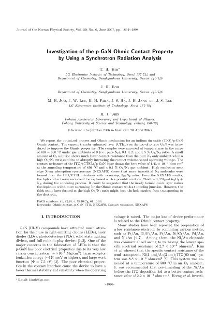
<strong>Investigation</strong> <strong>of</strong> <strong>the</strong> p-<strong>GaN</strong> <strong>Ohmic</strong> <strong>Contact</strong> <strong>Property</strong> <strong>by</strong>· · · – T. H. Kim et al. -1895-gated <strong>the</strong> <strong>Ohmic</strong> property <strong>of</strong> a Ni(10 nm)/ITO(250 nm)bilayer system [9]. The as-prepared electrode showedSchottky characteristics; on <strong>the</strong> o<strong>the</strong>r hand, <strong>the</strong> rapid<strong>the</strong>rmal processed one revealed a low resistance <strong>of</strong> 8.6 ×10 −4 ohm·cm 2 at a temperature <strong>of</strong> 600 ◦ C in an air atmosphere.It was suggested that <strong>the</strong> contact resistancewas lowered <strong>by</strong> an increase in <strong>the</strong> <strong>of</strong> hole carrier concentration,and that a p-type semiconductor NiO had beenformed at <strong>the</strong> interface.However, <strong>the</strong> external efficiency declines <strong>by</strong> less than50 % transmittance <strong>of</strong> <strong>the</strong> metal electrode in <strong>the</strong> visibleregion in spite <strong>of</strong> its having a good electrical property.Among <strong>the</strong> transparent conductive oxides, suchas indium tin oxide (ITO), aluminum-doped zinc oxide(AZO), indium zinc oxide (IZO) and cadmium tin oxide(CTO), ITO is a good candidate material to replace <strong>the</strong>semi-transparent metal electrode, because <strong>the</strong> transmittanceis more than 95 % and because it has good electricalproperties, such as low resistance (5 × 10 −4 ◦ C), highcarrier concentration (10 20 ∼ 10 21 /cm 3 ) and mobility (20∼ 25 cm 2 /V·S) [10–12]. The light extraction efficiency isexpected to increase to more than 10 % if <strong>the</strong> metal electrodeis used for ITO. When <strong>the</strong> ITO is directly depositedon <strong>the</strong> p-<strong>GaN</strong> semiconductor, <strong>the</strong> electrical property isnon-<strong>Ohmic</strong>. Therefore, a new process development isneeded to optimize <strong>the</strong> <strong>Ohmic</strong> contact property. Changet al. reported that a thin In 0.1 Ga 0.9 N layer insertedinto <strong>the</strong> ITO/p-<strong>GaN</strong> interface reduced <strong>the</strong> Schottky barrierheight [13]. The contact resistance was 4.5 × 10 −2ohm·cm 2 after annealing at a temperature <strong>of</strong> 500 ◦ C ina N 2 environment. They suggested that Ga-vacanciescreated <strong>by</strong> out-diffusion <strong>of</strong> gallium atoms played an importantrole in <strong>the</strong> <strong>Ohmic</strong> mechanism. Kuo et al. reportedthat <strong>the</strong> low resistance (1.2 × 10 −3 ohm·cm 2 )and a high transmittance (86.5 %) had been attained <strong>by</strong>inserting a Si-doped n + In<strong>GaN</strong>/<strong>GaN</strong> short-period superlattice(SPS) layer [14]. This layer was functioned as atunneling layer.According to <strong>the</strong> previous results, <strong>the</strong>re is a tendencyto adopt a high-transmittance electrode like ITO ra<strong>the</strong>rthan a semi-transparent metal electrode, although metalelectrode shows better electrical properties than ITOdoes. However, few works in <strong>the</strong> literature have addressedcurrently available processes and <strong>the</strong> mechanism<strong>of</strong> <strong>Ohmic</strong> contact, although many studies have been performedto improve <strong>the</strong> ITO/p-<strong>GaN</strong> <strong>Ohmic</strong> characteristics[15, 16]. In this study, we report optimized resultsfor <strong>the</strong> <strong>Ohmic</strong> properties <strong>by</strong> inserting a charge transportenhanced layer (CTEL), on n + In<strong>GaN</strong>/<strong>GaN</strong> superlattice.We also suggest <strong>the</strong> <strong>Ohmic</strong> mechanism between<strong>the</strong> p-<strong>GaN</strong>/CTEL and <strong>the</strong> ITO layer <strong>by</strong> using a surfaceanalysis and a synchrotron radiation analysis.II. EXPERIMENTThe epitaxial layer <strong>of</strong> <strong>the</strong> LED structure was grownon a sapphire substrate <strong>the</strong> using metal-organic chemicalvapor deposition (MOCVD). The LED structure is asfollows: a <strong>GaN</strong> nucleation layer deposited at 520 ◦ C, a 3µm-thick Si-doped <strong>GaN</strong> layer, a five period In<strong>GaN</strong>/<strong>GaN</strong>multiple quantum well (MQW), and a 0.15 µm-thick Mgdoped <strong>GaN</strong> layer. The Mg doping concentration <strong>of</strong> p-<strong>GaN</strong> was 1.2 × 10 20 /cm 3 . The charge transfer enhancedlayer (CTEL) deposited on p-<strong>GaN</strong> was a Si-doped In-<strong>GaN</strong>/<strong>GaN</strong> superlattice with a <strong>the</strong> because <strong>of</strong> several nm.The ITO electrode was deposited <strong>by</strong> using <strong>the</strong> R.F.-magnetron sputtering method and had a thickness <strong>of</strong>300 nm. The electrical properties were measured at variousannealing conditions for <strong>the</strong> ITO(30 nm)/CTEL(n +In<strong>GaN</strong>/<strong>GaN</strong>)/p − <strong>GaN</strong> sample. The operation voltages(Vop) were measured at 20 mA with a 375 × 330 µm 2lateral structure LED. The contact resistances were calculatedusing <strong>the</strong> circular-TLM method.ITO samples <strong>of</strong> 5 nm in thickness were specially designedto study <strong>the</strong> chemistry <strong>of</strong> interface reaction becauseit is impossible to investigate non-destructively <strong>the</strong>interface <strong>by</strong> inserting a CTEL overlayer as thick as 300nm. These samples were annealed at temperatures <strong>of</strong>(400 ◦ C, 650 ◦ C, and 800 ◦ C) in (pure N 2 , 0.1 % O 2 /N 2 ,0.2 % O 2 /N 2 , and 0.5 % O 2 /N 2 ). Surface and interfaceanalyses for <strong>the</strong> annealed samples were performed usingX-ray photoelectron spectroscopy (XPS), time-<strong>of</strong>-flightsecondary ion mass spectrometry (TOF-SIMS), scanningelectron microscopy (SEM), and atomic force microscopy(AFM). Near-edge X-ray absorption spectroscopy (NEX-AFS) was also utilized to analyze <strong>the</strong> chemical speciesnewly formed at <strong>the</strong> interface. The NEXAFS experimentwas conducted at <strong>the</strong> 8A1(U7) beam line in <strong>the</strong>Pohang Accelerator Laboratory (PAL). The spectra wereobtained <strong>by</strong> recording <strong>the</strong> sample current in total electronyield (TEY) mode as a function <strong>of</strong> energy. Theabsolute photon energy scale was referenced to <strong>the</strong> value<strong>of</strong> 401.10 eV, which position is <strong>the</strong> second π ∗ resonancepeak for gas phase N 2 .III. RESULTS AND DISCUSSIONFigure 1 shows <strong>the</strong> operation voltages (Vop) and contactresistances at a temperature <strong>of</strong> 650 ◦ C for variousambient conditions (pure N 2 , 0.1 % O 2 /N 2 , 0.2 % O 2 /N 2 ,and 0.5 % O 2 /N 2 ). The operation voltage (Vop) and <strong>the</strong>contact resistance are 3.38 V and 4 × 10 −2 ohm·cm 2 , respectively,for pure N 2 , reach <strong>the</strong>ir lowest values <strong>of</strong> 3.27V and 1.43 × 10 −3 ohm·cm 2 at a 0.1 % O 2 /N 2 ratio,and finally rise again to 3.53 V and 3.1 × 10 −1 ohm·cm 2with increasing rate <strong>of</strong> O 2 /N 2 ratio. It is noted that <strong>the</strong>addition <strong>of</strong> O 2 is undoubtedly required to achieve <strong>the</strong>optimum <strong>Ohmic</strong> condition during <strong>the</strong> annealing process;however, a large amount <strong>of</strong> O 2 can bring about a badeffect.Figure 2 shows <strong>the</strong> high-resolution N K-edge NEXAFSspectra for various conditions. As mentioned above, <strong>the</strong>NEXAFS technique is able to examine <strong>the</strong> interface reactionnon-destructively, unlike XPS, SIMS, and AES
-1896- Journal <strong>of</strong> <strong>the</strong> Korean Physical Society, Vol. 50, No. 6, June 2007Fig. 1. Electrical properties <strong>of</strong> <strong>the</strong> ITO electrode contactingCTEL/p-<strong>GaN</strong> annealed with O 2/N 2 % as a functional<strong>of</strong> <strong>the</strong> O 2/N 2 % ratio at 650 ◦ C: filled squares: Vop andtriangle: R c.Fig. 2. High-resolution N K-edge NEXAFS spectra <strong>of</strong>ITO electrode annealed at several O 2/N 2 % ratios at 650◦ C.Fig. 3. SEM micrograph and AFM topography image for a severely annealed ITO electrode (a) SEM Micrography (b) AFMTopography.analyses. The optimum thickness <strong>of</strong> <strong>the</strong> ITO overlayerwas chosen <strong>by</strong> <strong>the</strong> highest N K-edge intensity among <strong>the</strong>5 nm, 10 nm, 30 nm thicknesses. Then, NEXAFS datawere obtained from <strong>the</strong> ITO thickness <strong>of</strong> 5 nm. Althoughit is still controversial whe<strong>the</strong>r <strong>the</strong> N K-edge spectrumis due to ei<strong>the</strong>r atomic nitrogen or interstitial molecularN 2 , it has been concluded that <strong>the</strong> split high resolutionspectrum, N1s→ π ∗ orbital transition, originatesfrom <strong>the</strong> vibrational structure <strong>of</strong> N 2 molecules becausethis transition did not occur in <strong>the</strong> pre-annealing sample,<strong>the</strong> as-prepared one in dash-dot-dot line <strong>of</strong> <strong>the</strong> Figure 2.Similar results were also published in <strong>the</strong> previous studyon <strong>the</strong> SiON thin film [17]. In <strong>the</strong> N K-edge spectra, <strong>the</strong>molecular N 2 intensity increased in proportion to <strong>the</strong> O 2amount. This indicates that addition <strong>of</strong> O 2 during <strong>the</strong>annealing is essential to optimize <strong>the</strong> electrical propertieshowever, an increasing amount <strong>of</strong> O 2 does not alwaysfavor <strong>the</strong> contact resistance. That is, <strong>the</strong> electricalproperty shows an increasing tendency after an initialdecrease unlike <strong>the</strong> O 2 intensity. Though not shown inthis study, <strong>the</strong> molecular N 2 intensity increased with increasingtemperature from 400 ◦ C to 800 ◦ C in a 0.1% O 2 /N 2 ambient. There was no N 2 generation at <strong>the</strong>lowest annealing temperature <strong>of</strong> 400 ◦ C, irrespective <strong>of</strong><strong>the</strong> O 2 amount, however, <strong>the</strong> N 2 generation at occurredannealing temperatures <strong>of</strong> 650 ◦ C and 800 ◦ C and increasedwith increasing amount <strong>of</strong> O 2 . This indicatesthat generation <strong>of</strong> N 2 gas can cause Ga-vacancies, whichare created <strong>by</strong> out-diffusion <strong>of</strong> gallium atoms through <strong>the</strong>CTEL tunneling layer, resulting in a decrease in <strong>the</strong> electricalresistance <strong>of</strong> up to 1.2 × 10 −3 ohm·cm 2 ) betweena 0 % and a 0.1 % O 2 /N 2 ambient.
<strong>Investigation</strong> <strong>of</strong> <strong>the</strong> p-<strong>GaN</strong> <strong>Ohmic</strong> <strong>Contact</strong> <strong>Property</strong> <strong>by</strong>· · · – T. H. Kim et al. -1897-Figure 3 shows AFM and SEM micrograph images <strong>of</strong> aseverely annealed surface at a high temperature (800 ◦ C)for 1 hr. Bubbles that formed at <strong>the</strong> interface betweenITO and p-<strong>GaN</strong> are observed in <strong>the</strong> picture. The harshannealing condition leads to much more generation <strong>of</strong>N 2 gas. Then, <strong>the</strong> interface gets loose and <strong>the</strong> electricalproperty declines due to a reduction <strong>of</strong> <strong>the</strong> contact area,and device failure is induced <strong>by</strong> a local <strong>the</strong>rmal effect.From <strong>the</strong> above results, <strong>the</strong> <strong>Ohmic</strong> mechanism canbe considered from a correlation between <strong>the</strong> evolutionquantity <strong>of</strong> N 2 and <strong>the</strong> electrical properties. A chemicalreaction equation for N 2 evolution can be proposed asbelow:2<strong>GaN</strong> + 3/2O 2 → Ga 2 O 3 + N 2 (1)The Gibbs free energies <strong>of</strong> <strong>the</strong> <strong>GaN</strong> and <strong>the</strong> Ga 2 O 3 compoundsare −118.5 kJ/mol and −998.3 kJ/mol, respectively[18]. Since oxide is more <strong>the</strong>rmodynamically stablethan nitride, <strong>the</strong> direction <strong>of</strong> this reaction tends to <strong>the</strong>right. According to Eq. (1), <strong>the</strong> molecular N 2 observedin <strong>the</strong> NEXAFS spectrum would be produced <strong>by</strong> decomposition<strong>of</strong> <strong>GaN</strong> at a moderate condition, 650 ◦ C and0.1 % O 2 /N 2 . Then, hole transport might be expedited<strong>by</strong> tunneling through <strong>the</strong> thin oxide layer. However, athickly formed Ga 2 O 3 layer prevents hole carriers fromtransporting to <strong>the</strong> ITO electrode, and a large amount<strong>of</strong> N 2 can result in bubbling, which degrade <strong>the</strong> contactinterface under severe annealing conditions, as alreadyshown in Figure 3. This explains sufficiently <strong>the</strong> relation<strong>of</strong> annealing conditions and electrical properties. It isalso indicates that we have to search for <strong>the</strong> optimumrange <strong>of</strong> <strong>the</strong> process window to achieve <strong>the</strong> lowest operatingvoltage and contact resistance.It is known that inserting an insulating buffer layerenhances <strong>the</strong> tunneling property. Similar studies haveexamined <strong>the</strong> role <strong>of</strong> an insulating layer at <strong>the</strong> interfacein organic light emitting diodes [19, 20]. The reason isthat dipolar electrostatic charges <strong>of</strong> ionic bonding arepolarized at <strong>the</strong> interface between ITO (anode, hole injection)and a p-type semiconductor and <strong>the</strong> distribution<strong>of</strong> a dipolar layer helps <strong>the</strong> depletion width to narrow for<strong>Ohmic</strong> contact. The injection barrier height is, thus, reduced.IV. SUMMARYThe optimized process for a indium-tin oxide (ITO)/p-<strong>GaN</strong> <strong>Ohmic</strong> contact has been studied. The current transferenhanced layer (CTEL) was deposited on top <strong>of</strong> p-type <strong>GaN</strong> to reduce <strong>the</strong> Schottky barrier height. Thiswas annealed under <strong>the</strong> various annealing conditions toimprove <strong>the</strong> electrical property. The contact resistance<strong>of</strong> <strong>the</strong> ITO/p-<strong>GaN</strong> layer had its lowest value <strong>of</strong> 1.43 ×10 −3 ohm·cm 2 at a temperature <strong>of</strong> 650 ◦ C and a 0.1 %O 2 /N 2 ratio ambient. High-resolution near-edge X-rayabsorption spectroscopy (NEXAFS) and o<strong>the</strong>r surfaceanalytical techniques were used to investigate <strong>the</strong> reaction<strong>of</strong> <strong>the</strong> contact layer. The NEXAFS technique hasa merit in observing <strong>the</strong> interface non-destructively anddirectly observed <strong>the</strong> vibrationally resolved N K-edge absorptionspectra at <strong>the</strong> contact interface. We proposedthat <strong>the</strong> molecular N 2 would be formed from <strong>the</strong> reactionequation, 2<strong>GaN</strong> + 3/2O 2 →Ga 2 O 3 + N 2 , during <strong>the</strong>annealing process. The evolution <strong>of</strong> N 2 increases with increasingO 2 /N 2 % ratio and annealing temperature. Therelation between <strong>the</strong> electrical property and <strong>the</strong> annealingprocess was examined. It could be suggested that <strong>the</strong>newly formed oxide layer narrowed <strong>the</strong> depletion widthfor <strong>Ohmic</strong> contact with tunneling junction. However,a thick oxide layer and a large amount <strong>of</strong> N 2 evolutionmight prevent hole carriers from transporting to <strong>the</strong> electrode.ACKNOWLEDGMENTSSupport <strong>of</strong> this work from <strong>the</strong> Pohang AcceleratorLaboratory and from <strong>the</strong> BK21 project is appreciated.REFERENCES[1] S. Nakamura, T. Mukai and M. Senoh, Appl. Phys. Lett.67, 1868 (1995).[2] S. C. Binari, J. M. Redwing, G. Kelner and W. Kruppa,Electron. Lett. 30, 242 (1997).[3] W. Gotz, N. M. Johnson, J. Walker, D. P. Bour and R.A. Street, Appl. Phys. Lett. 68, 667 (1996).[4] H. Ishikawa, S. Kobayashi, Y. Koide, S. Yamasaki, S.Asami, N. Shibata and M. Koike, Appl. Phys. Lett. 69,3537 (1996).[5] Y. Koide, H. Ishikawa, S. Kobayasi, S. Yamasaki, S. Nagai,J. Umezaki, M. Koike and M. Murakami, J. Appl.Phys. 81, 1315 (1997).[6] T. Kim, M. C. Yoo and T. Kim, Mater. Res. Soc. Symp.Proc. 449, 1061 (1997).[7] D. J. King, S. D. Hersee, J. C. Ramer and L. Zhang,Mater. Res. Soc. Symp. Proc. 468, 421 (1997).[8] S. Y. Kim, H. W. Jang and J. L. Lee, Appl. Phys. Lett.82, 61 (2003).[9] R. H. Horng, D. S. Wuu, Y. C. Lien and W. H. Lan,Appl. Phys. Lett. 79, 2925 (2001).[10] D. W. Kim, Y. J. Sung, J. W. Park and G. Y. Yeom,Thin Solid Films 398-399, 87 (2001).[11] J. F. Lin, M. C. Wu, M. J. Jou, C. M. Chang, B. J. Leeand T. Y. Tsai, Electron Lett. 30, 1793 (1994).[12] D. R. Kammler, T. O. Mason, D. L. Young and J. T.Coutts, J. Appl. Phys. 90, 3263 (2001).[13] K. M. Chang, J. Y. Chu and C. C. Cheng, Solid-StateElectron. 49, 1381 (2005).[14] C. H. Kuo, S. J. Chang, Y. K. Su, R. W. Chuang, C. S.Chang, L. W. Wu, W. C. Lai, J. F. Chen, J. K. Sheu, H.M. Lo and J. M. Tsai, Mat. Sci. Eng. B 106, 69 (2004).[15] J. S. Kwak and Y. Park, J. Korean Phys. Soc. 45, 988(2004).
-1898- Journal <strong>of</strong> <strong>the</strong> Korean Physical Society, Vol. 50, No. 6, June 2007[16] S. W. Chae, J. S. Kwak, S. K. Yoon, M. Y. Kim, J. Song,T. Y. Seong and T. G. Kim, J. Korean Phys. Soc. 49,899 (2006).[17] Y. Chung, J. C. Lee and H. J. Shin, Appl. Phys. Lett.86, 022901 (2005).[18] O. Kubaschewski, C. B. Alock and P. J. Spencer, MaterialsThermochemistry (Pergamon, Oxford, 1993).[19] J. M. Zhao, S. T. Zhang, X. J. Wang, Y. Q. Zhan, X. Z.Wang, G. Y. Zhong, Z. J. Wang, X. M. Ding, W. Huangand X. Y. Hou, Appl. Phys. Lett. 84, 2913 (2004).[20] F. Zhu, B. Low, K. Zhang and S. Chua, Appl. Phys. Lett.79, 1205 (2001).