Fabrication of subwavelength-size aperture for a near ... - IEEE Xplore
Fabrication of subwavelength-size aperture for a near ... - IEEE Xplore
Fabrication of subwavelength-size aperture for a near ... - IEEE Xplore
- No tags were found...

Create successful ePaper yourself
Turn your PDF publications into a flip-book with our unique Google optimized e-Paper software.
<strong>Fabrication</strong> <strong>of</strong> <strong>subwavelength</strong>-<strong>size</strong> <strong>aperture</strong> <strong>for</strong> a <strong>near</strong>-field optical probeusing various micr<strong>of</strong>abrication proceduresS. S. Choi, a) M. Y. Jung, and D. W. KimDepartment <strong>of</strong> Physics, College <strong>of</strong> Natural Science, Sun Moon University, Ahsan, ChungNam336-708, KoreaJ. W. Kim and J. H. BooDepartment <strong>of</strong> Nanoscience and Technology, Sungkyunkwan University, Suwon, Kyung Gi-Do, KoreaReceived 18 July 2002; accepted 4 November 2002; published 23 December 2002We successfully fabricated <strong>subwavelength</strong>-<strong>size</strong> silicon oxide <strong>aperture</strong>s on a cantilever array as a<strong>near</strong>-field optical probe. Various semiconductor processes were utilized <strong>for</strong> <strong>subwavelength</strong>-<strong>size</strong><strong>aperture</strong> fabrication. The anisotropic etching <strong>of</strong> the Si substrate by alkaline solutions followed byanisotropic crystal orientation dependent oxidation, anisotropic plasma etching, and isotropic oxideetching was carried out. 2, 3, and 4 m <strong>size</strong> dot arrays were initially photolithographically patternedonaSi100 wafer. After fabrication <strong>of</strong> a V-groove shape by anisotropic etching, oxide growth at1000 °C was per<strong>for</strong>med to have an oxide etch mask. The oxide layer on the Si111 plane has beenutilized as an etch mask <strong>for</strong> plasma dry etching and water-diluted HF wet etching <strong>for</strong><strong>subwavelength</strong>-<strong>size</strong> <strong>aperture</strong> fabrication. A Au thin layer was deposited on the fabricated oxide<strong>aperture</strong> on the cantilever array. After this procedure, the initial opening, 300 nm <strong>of</strong> the oxide<strong>aperture</strong> was reduced down to 95 nm. © 2003 American Vacuum Society.DOI: 10.1116/1.1534574I. INTRODUCTIONThere has been considerable interest in fabricating a <strong>subwavelength</strong><strong>aperture</strong> <strong>for</strong> a <strong>near</strong>-field optical sensor due to itspotential application <strong>for</strong> promising <strong>near</strong>-field optical recordingand other biological applications. 1–3 Recently, there hasbeen a dramatic increase in storage density as high as 100Gbyte/in. 2 in <strong>near</strong>-field optical recording because it can circumventthe diffraction limit. 4–6 However, the low opticalpower generated through the tip <strong>of</strong> the fiber probe limits thescanning speed and hinders the development <strong>of</strong> the practicaloptical storage device. Recently, in order to improve the datarate, a parallel processing technique using a cantilever arrayseems to be the key solution <strong>for</strong> a faster data rate. 7–9 In thisarticle, nan<strong>of</strong>abrication techniques <strong>of</strong> a <strong>subwavelength</strong> <strong>aperture</strong>on the cantilever array using directional plasma etchingand isotropic buffered hydr<strong>of</strong>luoric acid BHF etching arepresented.<strong>Fabrication</strong> techniques <strong>for</strong> the <strong>subwavelength</strong>-<strong>size</strong> <strong>aperture</strong>array using the photoresist removal technique and sputteretching in addition to the focused ion beam milling havebeen reported. 1,3,4,10 The etching <strong>of</strong> Si using alkaline solutionssuch as KOH, ethylene-diamine/pyrocatechol EDP,and tetramethyl ammonium hydroxide TMAH, will be anisotropicdue to the different atomic densities <strong>of</strong> the Si crystalsurface. As the etch ratio <strong>of</strong> the Si100 surface to theSi111 surface is on the order <strong>of</strong> a few hundred, the intersection<strong>of</strong> the Si111 surfaces eventually will <strong>for</strong>m a V-typegroove or a pyramidal shape at the bottom Si100surface. 11–13 The oxidation rate is dependent upon both thecrystal plane and the angle <strong>of</strong> the plane intersection. Thea Author to whom correspondence should be addressed; electronic mail:sscphy@empal.comhigher packed Si111 surface will have a higher oxidationrate than the Si100 surface, especially <strong>for</strong> the surfacereactioncontrolled region. Retarded oxide growth from aconcave surface was also reported. The stress-induced retardation<strong>of</strong> oxidation can result from oxidation at temperaturelower than 950 °C or volume expansion <strong>of</strong> oxide at a concavesurface during thermal oxidation even at 1000 °C. 13–16The resultant thicker oxide on the Si111 surface than theSi100 bottom surface can be utilized as an etch mask duringeither the dry or wet etching procedure <strong>for</strong><strong>subwavelength</strong>-<strong>size</strong> <strong>aperture</strong> fabrication. Anisotropic dryetching was employed to provide a <strong>subwavelength</strong>-<strong>size</strong> <strong>aperture</strong>on the bottom <strong>of</strong> the V groove. Chlorine gas alone, orin a mixture with Ar gas is also known to be very effective inproviding an anisotropic directional process. 17 An isotropicwater-diluted HF solution etching technique has been alsoemployed to fabricate the <strong>subwavelength</strong>-<strong>size</strong> <strong>aperture</strong> at theapex <strong>of</strong> the oxide pyramid on the cantilever array.II. FABRICATION PROCEDURES ANDEXPERIMENTAL RESULTSThe key fabrication procedures in our experiments includei the deposition <strong>of</strong> oxide and nitride as an etch mask,ii <strong>for</strong>mation <strong>of</strong> inverted pyramids or V grooves using alkalinesolution, iii thermal oxidation <strong>of</strong> V-groove patterns,iv definition <strong>of</strong> the cantilever patterns, v fabrication <strong>of</strong> theoxide pyramid, vi fabrication <strong>of</strong> nano<strong>size</strong> <strong>aperture</strong>s, andvii the thin metal deposition process. A detailed schematic<strong>of</strong> the fabrication procedures is given in Fig. 1.A. <strong>Fabrication</strong> <strong>of</strong> <strong>subwavelength</strong>-<strong>size</strong> valleysAt first, 2, 3, and 4 m dot arrays were patterned onp-type 5–15 cm 4 in. Si wafers using the conventional118 J. Vac. Sci. Technol. B 21„1…, JanÕFeb 2003 1071-1023Õ2003Õ21„1…Õ118Õ5Õ$19.00 ©2003 American Vacuum Society 118
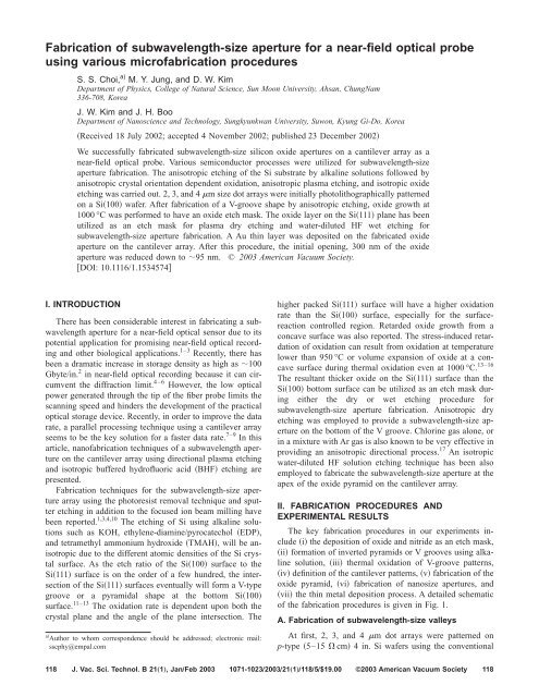
119 Choi et al.: <strong>Fabrication</strong> <strong>of</strong> <strong>subwavelength</strong>-<strong>size</strong> <strong>aperture</strong> 119FIG. 2. a SEM micrograph <strong>of</strong> KOH solution etched Si100 wafer presentsthe V groove <strong>of</strong> the 22 m 2 pattern. The Si111 surface intersects eachother at the bottom <strong>of</strong> the V groove. b The SEM micrograph presents theretarded oxidation on the bottom <strong>of</strong> the V groove white circled area. Thethicknesses <strong>of</strong> the oxides on the 54.7° angled Si111 surface and the narrowbottom Si100 surface are 330 and 100 nm, correspondingly.FIG. 1. Schematic <strong>of</strong> the fabrication procedures <strong>for</strong> the <strong>subwavelength</strong>-<strong>size</strong><strong>aperture</strong> on the cantilever array. a Opening <strong>for</strong> the etch window using anitride and oxide double layer as an etch mask, b <strong>for</strong>mation <strong>of</strong> the invertedpyramidal shape, c thermal oxidation, d definition <strong>of</strong> the cantilever patternand top view in d-1, c <strong>for</strong>mation <strong>of</strong> the hollow oxide pyramid, ffabrication <strong>of</strong> nano<strong>size</strong> <strong>aperture</strong>, and g metal thin film deposition.photolithographic technique. A double layer <strong>of</strong> 200-nmthicksilicon nitride and 250-nm-thick silicon oxide was dryetched <strong>for</strong> the opening window using reactive ion etchingRIE, as in Fig. 1a. The RIE etching conditions <strong>for</strong> themask layer were rf power 600 W, an etching gas mixture <strong>of</strong>CHF 3 10 sccm, CF 4 10 sccm, and O 2 20 sccm with an operatingpressure <strong>of</strong> 100 mTorr.40 wt % KOH solution will anisotropically etch the Sisubstrate with 1 m/s etch rate at 80 °C. KOH etching atlower temperature will have a slower etch rate, while it willresult in a nonuni<strong>for</strong>m etch surface at temperature higherthan 80 °C. On the other hand, 20 wt % TMAH solution at80 °C will etch anisotropically with an etch rate <strong>of</strong> 0.45m/s. The V-groove <strong>for</strong>mation with 2 m square patternswas carried out using KOH solution as in Fig. 1b. Thewidth <strong>of</strong> the opening (W m ) is related to etch depth t and thewidth <strong>of</strong> the etched silicon surface at the bottom (W Si )isasbelow:W m W Si 2t,etched Si111 surfaces will intersect each other to <strong>for</strong>m a Vgroove, when the opening is small enough. Even in the case<strong>of</strong> the V-groove <strong>for</strong>mation, the narrow bottom area at theSi100 surface would have a nanoscale area, as seen in Fig.2a.As a next step, Fig. 1c, thermal steam oxidation hasbeen per<strong>for</strong>med at 1000 °C <strong>for</strong> 72 min. The thickness <strong>of</strong> theoxide grown at the Si111 and Si100 bottom surfaces wasexamined by field emission scanning electron microscopySEM, and found to be 330 and 100 nm, respectively, asin Fig. 2b. The SEM micrograph reveals that the thickness<strong>of</strong> the oxide grown on the Si111 surface becomes thinner asit approaches the bottom <strong>of</strong> the V groove. This phenomenoncan be attributed to two reasons: i the oxidation rate at theSi100 surface is slower than that at the Si111 surface, andii the fact that the diffusion-controlled mechanism dominateson the concave region <strong>of</strong> the V-groove bottom. Theoxide growth will be severely retarded in a concave structuredue to the compressive stress since it would hinder the oxygendiffusion to the Si/SiO 2 interface. 13–16 Our experimentalresults <strong>for</strong> other 3-, 4-, 5-, and 10-m-square pattern Vgrooves also exhibited retarded oxidation <strong>of</strong> more than 50%.In order to fabricate a <strong>subwavelength</strong>-<strong>size</strong> <strong>aperture</strong>, twotechniques have been tried; one is to fabricate it with directionalplasma etching and the other is to utilize HF isotropicetching. Both techniques utilize the thicker oxide grown onthe Si111 plane as an etch mask. Inductively coupledplasma ICP etching was per<strong>for</strong>med to generate<strong>subwavelength</strong>-<strong>size</strong> <strong>aperture</strong>s at the bottom <strong>of</strong> the oxidepyramid. The operating conditions were 100 W rf power, 9mTorr operating pressure, 40 sccm Cl 2 feed gas, with a duration<strong>of</strong> 3–5 min. The rf power applied to supply the biasvoltage on the substrate was set to 200 W. The bias voltageswith coil rf power <strong>of</strong> 100 W were measured to be 500 V. Theetch rate <strong>of</strong> SiO 2 at the measured bias voltage <strong>of</strong> 500 V wasJVSTB-MicroelectronicsandNanometer Structures
122 Choi et al.: <strong>Fabrication</strong> <strong>of</strong> <strong>subwavelength</strong>-<strong>size</strong> <strong>aperture</strong> 122electron microscropy and a deposition system with betteruni<strong>for</strong>mity, it is expected that a diameter <strong>of</strong> the <strong>aperture</strong> <strong>of</strong>even less than 50 nm can be obtained.ACKNOWLEDGMENTThis work was supported by Grant No. KOSEF 2001-1-11400-008-2 from the Basic Research Program <strong>of</strong> the KoreaScience and Engineering Foundation.Presented at the 46th International Conference on Electron, Ion, and PhotonBeam Technology and Nan<strong>of</strong>abrication, Anaheim, CA, 28–31 May 2002.FIG. 7. SEM micrographs show the fabricated cantilever array with theAu-coated 160-nm-diam <strong>aperture</strong>. The double layer <strong>of</strong> 350 nm oxide and1 m nitride layer were initially utilized. The remaining oxide layer wouldbe 200 nm after the isotropic etching process. The Au thin film was sputterdeposited on the outside surface area <strong>of</strong> the oxide pyramidal probe.ICP etching, isotropic HF etching, and metal sputter deposition.Wet chemical etching <strong>of</strong> alkaline solution using thedouble layer <strong>of</strong> silicon nitride and SiO 2 as an etch maskprovides an inverted pyramid or a V-groove shape due to theanisotropic crystal orientation dependent etching. After theV-groove <strong>for</strong>mation, stress-dependent oxidation at 1000 °Cwas per<strong>for</strong>med and resulted in a thicker oxide on the inclinedSi111 surface than the bottom Si100 surface, regardless<strong>of</strong> the pattern <strong>size</strong>. This phenomenon can be attributed tocompressive stress-induced retarded oxide growth from theconcave surface.We have employed the isotropic HF etching techniqueusing 10:1 diluted HF to open the pyramidal oxide <strong>aperture</strong>son the cantilever array generated after removing bulk Si fromthe backside. The isotropic etching technique using waterdilutedHF solution requires careful handling because <strong>of</strong> thethin edges <strong>of</strong> the oxide tetrahedron. In order to reduce thefabricated oxide <strong>aperture</strong> <strong>size</strong>, in a controllable way, the Authin film was sputter deposited and the <strong>size</strong> <strong>of</strong> the openingwas reduced down to 95 nm with Au deposition <strong>of</strong> 170 nm.With proper instruments such as high resolution transmission1 R. C. Davis, C. C. Williams, and P. Neuzil, Appl. Phys. Lett. 66, 23091995.2 A. G. T. Ruiter, M. H. P. Moers, N. F. van Hulst, and M. de Boer, J. Vac.Sci. Technol. B 14, 597 1996.3 C. Mihalcea, W. Scholz, S. Werner, S. Munster, E. Oesterschulze, and R.Kassing, Appl. Phys. Lett. 68, 3531 1996.4 A. Partovi, D. Peale, M. Wuttig, C. A. Murray, G. Zydzik, L. Hopkins, K.Baldwin, W. S. Hopson, J. Wynn, J. Lopata, L. Dhar, R. Chichester, andJ. H. Yeh, Appl. Phys. Lett. 75, 1515 1999.5 Y. Martin, S. Rishton, and H. K. Wickramasinghe, Appl. Phys. Lett. 71, 11997.6 E. Betzig, J. K. Trautman, R. Wolfe, E. M. Gyory, P. L. Finn, M. H.Kryder, and C. H. Chang, Appl. Phys. Lett. 61, 142 1992.7 H. J. Mamin, B. D. Terris, L. S. Fan, S. Hoen, R. C. Barret, and D. Rugar,IBM J. Res. Dev. 39, 681 1995.8 P. Vettiger, M. Despont, V. Dreschler, U. Duerig, W. Haeberle, M. I.Lutwyche, H. E. Rothuize, R. Stutz, R. Widmer, and G. K. Binnig, IBMJ. Res. Dev. 44, 323 2000.9 Y. Mitsuhashi, Jpn. J. Appl. Phys., Part 1 37, 2079 1998.10 M. Y. Jung, I. W. Lyo, D. W. Kim, and S. S. Choi, J. Vac. Sci. Technol. A18, 1333 2000.11 H. Seidel, L. Csepregi, A. Heuberger, and H. Baumgartel, J. Electrochem.Soc. 137, 3612 1990.12 G. T. A. Kovacs, N. I. Maluf, and K. E. Peterson, Proc. <strong>IEEE</strong> 86, 15361998.13 M. Y. Jung, J. W. Lee, J. W. Kim, D. W. Kim, and S. S. Choi, Proceedings<strong>of</strong> the European Surface Science Meeting, Madrid, Spain, 6–9 September2000.14 D. B. Kao, J. P. McVittie, W. D. Nix, and K. C. Saraswat, <strong>IEEE</strong> Trans.Electron Devices ED-35, 251988.15 D. B. Kao, J. P. McVitte, W. D. Nix, and K. C. Saraswat, <strong>IEEE</strong> Trans.Electron Devices ED-34, 1008 1987.16 H. L. Liu, D. K. Biegelson, F. A. Ponse, N. M. Johnson, and R. F. W.Pease, Appl. Phys. Lett. 64, 1383 1994.17 H. F. Winters and J. W. Coburn, J. Vac. Sci. Technol. B 3, 13761985.J. Vac. Sci. Technol. B, Vol. 21, No. 1, JanÕFeb 2003