Fabrication of subwavelength-size aperture for a near ... - IEEE Xplore
Fabrication of subwavelength-size aperture for a near ... - IEEE Xplore
Fabrication of subwavelength-size aperture for a near ... - IEEE Xplore
- No tags were found...

You also want an ePaper? Increase the reach of your titles
YUMPU automatically turns print PDFs into web optimized ePapers that Google loves.
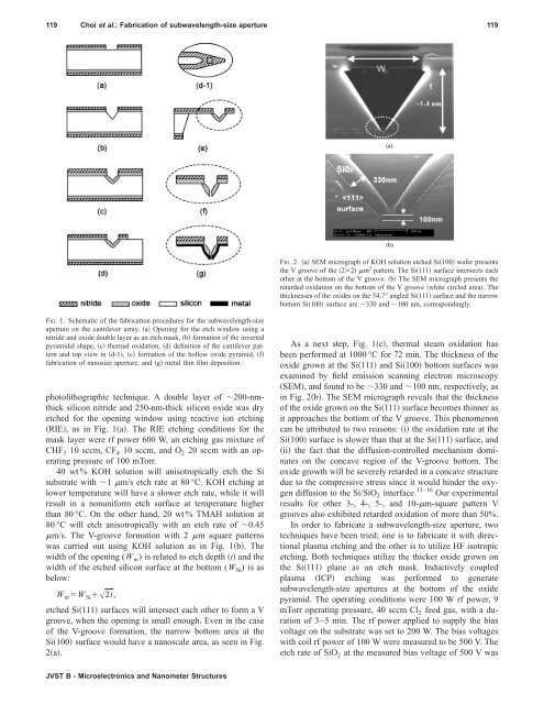
119 Choi et al.: <strong>Fabrication</strong> <strong>of</strong> <strong>subwavelength</strong>-<strong>size</strong> <strong>aperture</strong> 119FIG. 2. a SEM micrograph <strong>of</strong> KOH solution etched Si100 wafer presentsthe V groove <strong>of</strong> the 22 m 2 pattern. The Si111 surface intersects eachother at the bottom <strong>of</strong> the V groove. b The SEM micrograph presents theretarded oxidation on the bottom <strong>of</strong> the V groove white circled area. Thethicknesses <strong>of</strong> the oxides on the 54.7° angled Si111 surface and the narrowbottom Si100 surface are 330 and 100 nm, correspondingly.FIG. 1. Schematic <strong>of</strong> the fabrication procedures <strong>for</strong> the <strong>subwavelength</strong>-<strong>size</strong><strong>aperture</strong> on the cantilever array. a Opening <strong>for</strong> the etch window using anitride and oxide double layer as an etch mask, b <strong>for</strong>mation <strong>of</strong> the invertedpyramidal shape, c thermal oxidation, d definition <strong>of</strong> the cantilever patternand top view in d-1, c <strong>for</strong>mation <strong>of</strong> the hollow oxide pyramid, ffabrication <strong>of</strong> nano<strong>size</strong> <strong>aperture</strong>, and g metal thin film deposition.photolithographic technique. A double layer <strong>of</strong> 200-nmthicksilicon nitride and 250-nm-thick silicon oxide was dryetched <strong>for</strong> the opening window using reactive ion etchingRIE, as in Fig. 1a. The RIE etching conditions <strong>for</strong> themask layer were rf power 600 W, an etching gas mixture <strong>of</strong>CHF 3 10 sccm, CF 4 10 sccm, and O 2 20 sccm with an operatingpressure <strong>of</strong> 100 mTorr.40 wt % KOH solution will anisotropically etch the Sisubstrate with 1 m/s etch rate at 80 °C. KOH etching atlower temperature will have a slower etch rate, while it willresult in a nonuni<strong>for</strong>m etch surface at temperature higherthan 80 °C. On the other hand, 20 wt % TMAH solution at80 °C will etch anisotropically with an etch rate <strong>of</strong> 0.45m/s. The V-groove <strong>for</strong>mation with 2 m square patternswas carried out using KOH solution as in Fig. 1b. Thewidth <strong>of</strong> the opening (W m ) is related to etch depth t and thewidth <strong>of</strong> the etched silicon surface at the bottom (W Si )isasbelow:W m W Si 2t,etched Si111 surfaces will intersect each other to <strong>for</strong>m a Vgroove, when the opening is small enough. Even in the case<strong>of</strong> the V-groove <strong>for</strong>mation, the narrow bottom area at theSi100 surface would have a nanoscale area, as seen in Fig.2a.As a next step, Fig. 1c, thermal steam oxidation hasbeen per<strong>for</strong>med at 1000 °C <strong>for</strong> 72 min. The thickness <strong>of</strong> theoxide grown at the Si111 and Si100 bottom surfaces wasexamined by field emission scanning electron microscopySEM, and found to be 330 and 100 nm, respectively, asin Fig. 2b. The SEM micrograph reveals that the thickness<strong>of</strong> the oxide grown on the Si111 surface becomes thinner asit approaches the bottom <strong>of</strong> the V groove. This phenomenoncan be attributed to two reasons: i the oxidation rate at theSi100 surface is slower than that at the Si111 surface, andii the fact that the diffusion-controlled mechanism dominateson the concave region <strong>of</strong> the V-groove bottom. Theoxide growth will be severely retarded in a concave structuredue to the compressive stress since it would hinder the oxygendiffusion to the Si/SiO 2 interface. 13–16 Our experimentalresults <strong>for</strong> other 3-, 4-, 5-, and 10-m-square pattern Vgrooves also exhibited retarded oxidation <strong>of</strong> more than 50%.In order to fabricate a <strong>subwavelength</strong>-<strong>size</strong> <strong>aperture</strong>, twotechniques have been tried; one is to fabricate it with directionalplasma etching and the other is to utilize HF isotropicetching. Both techniques utilize the thicker oxide grown onthe Si111 plane as an etch mask. Inductively coupledplasma ICP etching was per<strong>for</strong>med to generate<strong>subwavelength</strong>-<strong>size</strong> <strong>aperture</strong>s at the bottom <strong>of</strong> the oxidepyramid. The operating conditions were 100 W rf power, 9mTorr operating pressure, 40 sccm Cl 2 feed gas, with a duration<strong>of</strong> 3–5 min. The rf power applied to supply the biasvoltage on the substrate was set to 200 W. The bias voltageswith coil rf power <strong>of</strong> 100 W were measured to be 500 V. Theetch rate <strong>of</strong> SiO 2 at the measured bias voltage <strong>of</strong> 500 V wasJVSTB-MicroelectronicsandNanometer Structures