Growth of Boron Nitride Thin Films on Silicon Substrates Using New ...
Growth of Boron Nitride Thin Films on Silicon Substrates Using New ...
Growth of Boron Nitride Thin Films on Silicon Substrates Using New ...

Create successful ePaper yourself
Turn your PDF publications into a flip-book with our unique Google optimized e-Paper software.
J.-H. Boo et al.: <str<strong>on</strong>g>Growth</str<strong>on</strong>g> <str<strong>on</strong>g>of</str<strong>on</strong>g> <str<strong>on</strong>g>Bor<strong>on</strong></str<strong>on</strong>g> <str<strong>on</strong>g>Nitride</str<strong>on</strong>g> <str<strong>on</strong>g>Thin</str<strong>on</strong>g> <str<strong>on</strong>g>Films</str<strong>on</strong>g> <strong>on</strong> Si 705phys. stat. sol. (a) 176, 705 (1999)Subject classificati<strong>on</strong>: 68.55.Jk; 78.20.Ci; S7.14<str<strong>on</strong>g>Growth</str<strong>on</strong>g> <str<strong>on</strong>g>of</str<strong>on</strong>g> <str<strong>on</strong>g>Bor<strong>on</strong></str<strong>on</strong>g> <str<strong>on</strong>g>Nitride</str<strong>on</strong>g> <str<strong>on</strong>g>Thin</str<strong>on</strong>g> <str<strong>on</strong>g>Films</str<strong>on</strong>g><strong>on</strong> Silic<strong>on</strong> <strong>Substrates</strong> <strong>Using</strong> <strong>New</strong> Organobor<strong>on</strong> PrecursorsJ.-H. Boo 1 † (a), C. Rohr (b), and W. Ho (b)(a) Institute <str<strong>on</strong>g>of</str<strong>on</strong>g> Basic Science and Department <str<strong>on</strong>g>of</str<strong>on</strong>g> Chemistry, Sungkyunkwan University,Suw<strong>on</strong> 440-746, Korea(b) Laboratory <str<strong>on</strong>g>of</str<strong>on</strong>g> Atomic and Solid State Physics and Department <str<strong>on</strong>g>of</str<strong>on</strong>g> Physics,Cornell University, Ithaca, NY 14853, USA(Received July 4, 1999)<str<strong>on</strong>g>Thin</str<strong>on</strong>g> films <str<strong>on</strong>g>of</str<strong>on</strong>g> BN have been deposited <strong>on</strong> silic<strong>on</strong> substrates in the temperature range <str<strong>on</strong>g>of</str<strong>on</strong>g> 600 to900 C by supers<strong>on</strong>ic molecular jet epitaxy and plasma-assisted MOCVD using new organobor<strong>on</strong>precursors such as borane-triethylamine complex (BTEA) and tris(sec-butyl)borane (TSBB). Hydrogenwas used as carrier gas, and additi<strong>on</strong>al nitrogen and amm<strong>on</strong>ia as reactive gases were suppliedby either through nozzle or via remoted plasma. Crack-free, polycrystalline hexag<strong>on</strong>al BNfilms with nano-size crystals were successfully grown at temperature as low as 750 C using BTEA.With increasing substrate temperatures to 900 C, however, the h-BN films chenged polycrystallinewith smoother surface and larger crystals. The changes <str<strong>on</strong>g>of</str<strong>on</strong>g> relative film quality with depositi<strong>on</strong> temperatureand reactive gas have been c<strong>on</strong>firmed with FTIR. Nitrogen plasma enhanced the filmquality and the stoichiometry, and removed the surface carb<strong>on</strong> effectively rather than amm<strong>on</strong>iaand hydrogen plasmas molecular beam. Wide band gaps were calculated using optical transmittancemeasurements.1. Introducti<strong>on</strong><str<strong>on</strong>g>Bor<strong>on</strong></str<strong>on</strong>g> nitride (BN) has received c<strong>on</strong>siderable attenti<strong>on</strong> due to its excepti<strong>on</strong>al propertiessuch as extreme hardness, high thermal c<strong>on</strong>ductivity, inertness, transparency, anddielectricity [1, 2]. These properties make BN an interesting material for many applicati<strong>on</strong>ssuch as protective and optical coatings, mask substrate for X-ray lithography, andinsulating layers in electr<strong>on</strong>ic devices [2, 3]. Besides <str<strong>on</strong>g>of</str<strong>on</strong>g> these applicati<strong>on</strong>s, moreover,thin films <str<strong>on</strong>g>of</str<strong>on</strong>g> BN are useful for the growth <str<strong>on</strong>g>of</str<strong>on</strong>g> GaN and diam<strong>on</strong>d films <strong>on</strong> Si due to theexcellent lattice mismatch between GaN (or diam<strong>on</strong>d) and BN [4]. Hexag<strong>on</strong>al BN(h-BN) has good tribological properties that are not degraded in air, otherwise cubicBN (c-BN) has almost the same hardness and thermal c<strong>on</strong>ductivity as diam<strong>on</strong>d. Underthe c<strong>on</strong>diti<strong>on</strong>s <str<strong>on</strong>g>of</str<strong>on</strong>g> high pressure and temperature, h-BN transforms into a wurtzite w-BNor a cubic c-BN. Up to now, however, it was very difficult to make high quality BN thinfilms <strong>on</strong> Si due to the large lattice mismatch (about 33%). Because <str<strong>on</strong>g>of</str<strong>on</strong>g> good step coverage,CVD techniques are interesting for the synthesis <str<strong>on</strong>g>of</str<strong>on</strong>g> BN films, since they allows aprecise c<strong>on</strong>trol <str<strong>on</strong>g>of</str<strong>on</strong>g> the depositi<strong>on</strong> characteristics even <strong>on</strong> substrates with complex shape[5]. Furthermore, low-pressure synthesis permitting the formati<strong>on</strong> <str<strong>on</strong>g>of</str<strong>on</strong>g> pure and well-crys-1 ) Corresp<strong>on</strong>ding author; Tel.: +82-331-290-7072; Fax: +82-331-290-7075;e-mail: jhboo@chem.skku.ac.kr
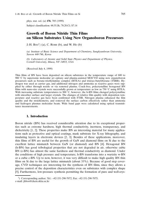
706 J.-H. Boo et al.tallized c-BN by a CVD method without i<strong>on</strong> bombardment was not successful so far [6].Thus, a new c<strong>on</strong>cept for a low-pressure synthesis must still be found for achieving highquality BN films. Plasma processing is becoming an increasingly important area in materialsand electr<strong>on</strong>ics research, and a depositi<strong>on</strong> method with a remote plasma systemto assist the growth seems to be a promising experiment.The CVD preparati<strong>on</strong> <str<strong>on</strong>g>of</str<strong>on</strong>g> BN films is usually carried out using toxic and explosivematerials such as diborane (B 2 H 6 ) or highly corrosive bor<strong>on</strong>trihalides such as BCl 3 . Inrecent years, there has therefore been great interest in the depositi<strong>on</strong> <str<strong>on</strong>g>of</str<strong>on</strong>g> BN with lessor n<strong>on</strong>-toxic organometallic precursors, especially single molecular precursors that c<strong>on</strong>tainboth bor<strong>on</strong> and nitrogen atoms in the same molecule. Only few papers have beenpublished using bor<strong>on</strong>-organic substances [7 to 10] and single molecular precursors [11to 14], most <str<strong>on</strong>g>of</str<strong>on</strong>g> them using borazine that has the disadvantage <str<strong>on</strong>g>of</str<strong>on</strong>g> instability at roomtemperature [13].To supply a buffer layers for the growth <str<strong>on</strong>g>of</str<strong>on</strong>g> GaN and AlN thin films, therefore, we firstlytried to deposit thin films <str<strong>on</strong>g>of</str<strong>on</strong>g> h-BN <strong>on</strong> Si substrates in the temperature range <str<strong>on</strong>g>of</str<strong>on</strong>g> 600 to900 C by supers<strong>on</strong>ic molecular jet epitaxy and plasma assisted MOCVD using new organobor<strong>on</strong>precursors such as BTEA and TSBB. These precursors have the advantage overmost others <str<strong>on</strong>g>of</str<strong>on</strong>g> being n<strong>on</strong>-toxic and n<strong>on</strong>-explosive and having suitable vapor pressures.2. ExperimentalThe experiments were carried out in a CVD chamber with a remote microwave plasmasystem. BTEA, …CH 3 CH 2 † 2BH 2 : BH 3 , and TSBB, ‰CH 3 CH 2 CH…CH 3 †Š 3B, were used asprecursors, and freeze-pump-thaw cycles were employed for the purificati<strong>on</strong> <str<strong>on</strong>g>of</str<strong>on</strong>g> the precursors.H 2 was used as carrier gas, and additi<strong>on</strong>al NH 3 and N 2 as reactive gases weresupplied by either through nozzle (orifice size: 150 mm) or via microwave (2.5 GHz)remoted plasma. The substrates were indirectly heated up to 900 C using a BN heater.The substrate temperatures were m<strong>on</strong>itored by an IR optical pyrometer. The base pressure<str<strong>on</strong>g>of</str<strong>on</strong>g> CVD system was 2 10 7 Torr while the CVD pressure was (3 to 4) 10 3 Torr.The typical growth time was 6 h and the average growth rate was approximately200 nm/h. The as-grown films were characterized with AES, XRD, TEM, AFM, andFTIR. Wide band gaps were calculated using optical transmittance measurements. Thedetails <str<strong>on</strong>g>of</str<strong>on</strong>g> experimental set-up and depositi<strong>on</strong> procedure are given in elsewhere [14].3. Results and Discussi<strong>on</strong>Highly oriented, crack-free, polycrystalline h-BN films were successfully obtained <strong>on</strong>Si(100) substrates at 900 C using both BTEA and TSBB. The Auger electr<strong>on</strong> spectra<str<strong>on</strong>g>of</str<strong>on</strong>g> the BN films grown <strong>on</strong> Si(100) with BTEA (Fig. 1a) and TSBB (Fig. 1b) at 900 Cshow two main peaks <str<strong>on</strong>g>of</str<strong>on</strong>g> B(KLL) and N(KLL) appearing at 180 and 380 eV, signifyingthe formati<strong>on</strong> <str<strong>on</strong>g>of</str<strong>on</strong>g> BN film <strong>on</strong> Si(100) surface. In additi<strong>on</strong>, two satellite peaks (e.g., Augerfine structure) become visible at 25 and 9 eV higher kinetic energy from the180 and 380 eV peaks. These satellite peaks are attributed to a bulk plasm<strong>on</strong> loss peakand a p plasm<strong>on</strong> loss peak <str<strong>on</strong>g>of</str<strong>on</strong>g> the sp 2 -b<strong>on</strong>ded h-BN, respectively [15]. Fig. 1a reveals aB :N ratio <str<strong>on</strong>g>of</str<strong>on</strong>g> about 1 :1 near the surface. If the precursor (BTEA) and H 2 carrier gaswere used without the NH 3 supers<strong>on</strong>ic jet or N 2 plasma, the obtained films have anexcess <str<strong>on</strong>g>of</str<strong>on</strong>g> carb<strong>on</strong> and a deficiency <str<strong>on</strong>g>of</str<strong>on</strong>g> nitrogen in the film. As shown in Fig. 1b, there
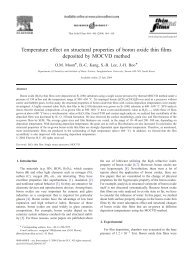
<str<strong>on</strong>g>Growth</str<strong>on</strong>g> <str<strong>on</strong>g>of</str<strong>on</strong>g> <str<strong>on</strong>g>Bor<strong>on</strong></str<strong>on</strong>g> <str<strong>on</strong>g>Nitride</str<strong>on</strong>g> <str<strong>on</strong>g>Thin</str<strong>on</strong>g> <str<strong>on</strong>g>Films</str<strong>on</strong>g> <strong>on</strong> Si 707Fig. 1. Auger electr<strong>on</strong> spectra <str<strong>on</strong>g>of</str<strong>on</strong>g> h-BN filmsgrown <strong>on</strong> Si(100) substrates at 900 C witha) borane-triethylamine complex and b) tris(-sec-butyl)boranealso appears a large C(KLL) Augerpeak due to surface c<strong>on</strong>taminati<strong>on</strong> fromthe precursor (TSBB) during depositi<strong>on</strong>.The B :N ratio <str<strong>on</strong>g>of</str<strong>on</strong>g> this film is 1 :0.7,suggesting that the amm<strong>on</strong>ia and nitrogencan easily remove the surface nitrogenrather than the surface carb<strong>on</strong>.Because FTIR spectra provide directinformati<strong>on</strong> about the local b<strong>on</strong>ding envir<strong>on</strong>ment<str<strong>on</strong>g>of</str<strong>on</strong>g> the c<strong>on</strong>stituents <strong>on</strong> thefilm, the changes <str<strong>on</strong>g>of</str<strong>on</strong>g> relative film qualitywith depositi<strong>on</strong> temperature and reactivegas can easily be c<strong>on</strong>firmed withFTIR. For h-BN films, there are twocharacteristic peaks at about 1400 and800 cm 1 , which are attributed to thein-plane B±N stretching and out-<str<strong>on</strong>g>of</str<strong>on</strong>g>planeB±N±B bending vibrati<strong>on</strong>s [16].For c-BN films, however, <strong>on</strong>ly <strong>on</strong>e peakwas observed at about 1100 cm 1 . Fig. 2shows the changes <str<strong>on</strong>g>of</str<strong>on</strong>g> FTIR spectrawhich are obtained from the BN filmsgrown <strong>on</strong> Si(100) with BTEA at variousdepositi<strong>on</strong> temperatures (Fig. 2a) andunder different reactive gas c<strong>on</strong>diti<strong>on</strong>s (Fig. 2b). With increasing depositi<strong>on</strong> temperaturesup to 900 C, the FWHMs <str<strong>on</strong>g>of</str<strong>on</strong>g> Fig. 2a become smaller, indicating that high qualityh-BN film can be deposited at higher temperature. With lower depositi<strong>on</strong> temperatures,the FTIR peak at about 1400 cm 1 broadens and slightly shifts towards lower wavenumbers. On the sides <str<strong>on</strong>g>of</str<strong>on</strong>g> the peak shoulders become obvious and <strong>on</strong>e can see `sidepeaks' at 1200 to 1250 and 1500 cm 1 associated with hydrogenated amorphous BNfilms. This indicates that hydrogenated amorphous BN films were obtained with BTEAbelow 750 C. Fig. 2b shows that the N 2 plasma enhanced the film quality and removedthe surface carb<strong>on</strong> effectively rather than NH 3 supers<strong>on</strong>ic molecular beam or H 2 plasma.This can be explained by the fact that N 2 with additi<strong>on</strong>al energy gained from theplasma is a better reactant with bor<strong>on</strong> from the precursor resulting in better films comparedto NH 3 . Because the NH 3 molecule has <strong>on</strong>e nitrogen atom b<strong>on</strong>ded to threehydrogen atoms it is more stable than the excited N 2 which can react more easily.Thus, it can be expected that the best BN films with high quality and good stoichiometrycould be deposited at 900 C with BTEA and N 2 plasma rather than withTSBB and NH 3 or H 2 .
708 J.-H. Boo et al.Fig. 2. FTIR spectra <str<strong>on</strong>g>of</str<strong>on</strong>g> h-BN filmsgrown <strong>on</strong> Si(100) substrates with a) borane-triethylaminecomplex at various depositi<strong>on</strong>temperatures, and b) under differentreactive gas c<strong>on</strong>diti<strong>on</strong>sDue to the small X-ray cross-secti<strong>on</strong>area <str<strong>on</strong>g>of</str<strong>on</strong>g> bor<strong>on</strong> which is <strong>on</strong>e <str<strong>on</strong>g>of</str<strong>on</strong>g>the light elements, it is very difficultto obtain a good XRD pattern <str<strong>on</strong>g>of</str<strong>on</strong>g>BN thin film. With a Read cameraand the exposure <str<strong>on</strong>g>of</str<strong>on</strong>g> 8 h, however, aclear picture <str<strong>on</strong>g>of</str<strong>on</strong>g> Debye-Scherrer diffracti<strong>on</strong>(see Fig. 3a) could be obtainedfrom the BN film grown withBTEA at 900 C. The existence <str<strong>on</strong>g>of</str<strong>on</strong>g>diffracti<strong>on</strong> rings indicates the presence<str<strong>on</strong>g>of</str<strong>on</strong>g> crystalline material. With atransparency scale, <strong>on</strong>e can identifydirectly the lattice spacings associatedwith the diffracti<strong>on</strong> rings andthe (hkl) planes <str<strong>on</strong>g>of</str<strong>on</strong>g> h-BN. For a singlecrystal <strong>on</strong>e would obtain a diffracti<strong>on</strong>pattern c<strong>on</strong>sisting <str<strong>on</strong>g>of</str<strong>on</strong>g> points,but as there are complete rings evenwithout any variati<strong>on</strong> in intensity, itsignifies that the material is randomlyoriented polycrystalline. Inthis study, we found seven different crystal planes, indicating a polycrystalline nature <str<strong>on</strong>g>of</str<strong>on</strong>g>the BN film. The fuzzyness <str<strong>on</strong>g>of</str<strong>on</strong>g> the outer rings is due to the small crystalline size. Inorder to determine the crystallinity <str<strong>on</strong>g>of</str<strong>on</strong>g> h-BN films in more detail, a plan-view TEMimage was obtained using the same film as in Fig. 3a. In Fig. 3b, <strong>on</strong>e can see that thefilm c<strong>on</strong>sists mainly <str<strong>on</strong>g>of</str<strong>on</strong>g> crystals <str<strong>on</strong>g>of</str<strong>on</strong>g> 100 to 300 nm size. The black `balls' are crystallites <str<strong>on</strong>g>of</str<strong>on</strong>g>a size <str<strong>on</strong>g>of</str<strong>on</strong>g> roughly 200 nm. With AFM, the morphology could be visualized even better.Fig. 3c shows the film surface seen from an angle to create a three-dimensi<strong>on</strong>al image.In Fig. 3c, the surface <str<strong>on</strong>g>of</str<strong>on</strong>g> BN film deposited <strong>on</strong> Si(100) at 900 C with BTEA showsnano-size crystallites with a root mean square (rms) roughness <str<strong>on</strong>g>of</str<strong>on</strong>g> 7.0 nm and peak-topeakroughness <str<strong>on</strong>g>of</str<strong>on</strong>g> about 100 nm. Only a few grains are as big as 1 to 2 mm. Ichiki etal. [17] reported that <strong>on</strong> the nanometer scale, the surface <str<strong>on</strong>g>of</str<strong>on</strong>g> h-BN film is rougherthan that <str<strong>on</strong>g>of</str<strong>on</strong>g> c-BN film. Therefore, our plan-view AFM image is c<strong>on</strong>sistent with thehexag<strong>on</strong>al nature <str<strong>on</strong>g>of</str<strong>on</strong>g> the BN film.Optical transmissi<strong>on</strong> data were also taken from the h-BN membranes fabricated byetching away a 0.25 inch diameter Si substrates. Fig. 4a shows that the BN film grown at900 C with BTEA has a high transmittance <str<strong>on</strong>g>of</str<strong>on</strong>g> about 80% in the infrared, throughoutthe visible and into the UV, where it drops sharply <str<strong>on</strong>g>of</str<strong>on</strong>g>f to zero indicating the band-edge
<str<strong>on</strong>g>Growth</str<strong>on</strong>g> <str<strong>on</strong>g>of</str<strong>on</strong>g> <str<strong>on</strong>g>Bor<strong>on</strong></str<strong>on</strong>g> <str<strong>on</strong>g>Nitride</str<strong>on</strong>g> <str<strong>on</strong>g>Thin</str<strong>on</strong>g> <str<strong>on</strong>g>Films</str<strong>on</strong>g> <strong>on</strong> Si 709Fig. 3. Debye-Scherrer diffracti<strong>on</strong> pattern, TEM and AFM images <str<strong>on</strong>g>of</str<strong>on</strong>g> h-BN films grown <strong>on</strong> Si(100)at 900 C with borane-triethylamine complex a) Debye-Scherrer diffracti<strong>on</strong> pattern, b) TEM, andc) AFM<str<strong>on</strong>g>of</str<strong>on</strong>g> the material. With the straight-line intercepti<strong>on</strong> at about 215 nm wavelength, an energyband gap <str<strong>on</strong>g>of</str<strong>on</strong>g> 5.8 eV was deduced. This is in exact agreement with the reportedvalue for the band gap <str<strong>on</strong>g>of</str<strong>on</strong>g> h-BN [2, 18, 19]. On the other hand, Fig. 4b for a h-BN filmgrown at 900 C with TSBB shows rather smaller transmissi<strong>on</strong> compared with that <str<strong>on</strong>g>of</str<strong>on</strong>g>Fig. 4a, signifying poor crystallinity. This can reflect a difference <str<strong>on</strong>g>of</str<strong>on</strong>g> carb<strong>on</strong> c<strong>on</strong>tents inthe film layer, that is, the carb<strong>on</strong> c<strong>on</strong>taminati<strong>on</strong> lowers the transmittance c<strong>on</strong>siderablyFig. 4. Optical transmittance data <str<strong>on</strong>g>of</str<strong>on</strong>g> h-BN films grown <strong>on</strong> Si(100) substrates at 900 C with a) borane-triethylaminecomplex, and b) tris(sec-butyl)borane24 physica (a) 176/1
710 J.-H. Boo et al.: <str<strong>on</strong>g>Growth</str<strong>on</strong>g> <str<strong>on</strong>g>of</str<strong>on</strong>g> <str<strong>on</strong>g>Bor<strong>on</strong></str<strong>on</strong>g> <str<strong>on</strong>g>Nitride</str<strong>on</strong>g> <str<strong>on</strong>g>Thin</str<strong>on</strong>g> <str<strong>on</strong>g>Films</str<strong>on</strong>g> <strong>on</strong> Siand cuts it <str<strong>on</strong>g>of</str<strong>on</strong>g>f at around 250 nm. Thus, <strong>on</strong>e can estimate a band gap <str<strong>on</strong>g>of</str<strong>on</strong>g> 5.0 eV fromFig. 4b. For h-BN, however, the results from literature differ and it is not clear if theband gap is direct [18] or indirect [19]. In this study, an indirect band gap (5.8 eV) forh-BN in-plane lattice spacing is taken for comparis<strong>on</strong>.4. C<strong>on</strong>clusi<strong>on</strong>sHighly oriented polycrystalline, crack-free h-BN films in [002] and [101] directi<strong>on</strong>s weresuccessfully deposited <strong>on</strong> Si(100) substrates at temperature as low as 750 C usingBTEA. Below 750 C, <strong>on</strong> the other hand, hydrogenated amorphous BN films were alsoobtained with both BTEA and TSBB. The changes <str<strong>on</strong>g>of</str<strong>on</strong>g> relative film quality with depositi<strong>on</strong>temperature and reactive gas have been c<strong>on</strong>firmed by FTIR spectroscopy. Nitrogen plasmaenhanced the film quality and the stoichiometry and removed the surface carb<strong>on</strong>effectively rather than amm<strong>on</strong>ia molecular beam and hydrogen plasma. The best BNfilms with high quality and good stoichiometry could be deposited at 900 C with BTEAand nitrogen plasma rather than with TSBB and amm<strong>on</strong>ia or hydrogen. Wide band gap(5.8 eV) was calculated from optical transmittance data, and the carb<strong>on</strong> c<strong>on</strong>taminati<strong>on</strong> inthe film layer can lower the transmittance c<strong>on</strong>siderably. To our best knowledge, this is thefirst report <str<strong>on</strong>g>of</str<strong>on</strong>g> growing BN films from the precursors <str<strong>on</strong>g>of</str<strong>on</strong>g> BTEA and TSBB.Acknowledgements One <str<strong>on</strong>g>of</str<strong>on</strong>g> authors (J.-H. B.) thanks the Korean Research Foundati<strong>on</strong>(Grant No. D00036) and the Sungkyunkwan University for their financial supports.Support <str<strong>on</strong>g>of</str<strong>on</strong>g> this research by the BMDO via ONR Grant No. N00014-93-0499 and SBIRvia ONR c<strong>on</strong>tact No. N00014-95-C-0414 is gratefully acknowledged.References[1] J. H. Edgar, in: Properties <str<strong>on</strong>g>of</str<strong>on</strong>g> Group III <str<strong>on</strong>g>Nitride</str<strong>on</strong>g>s; EMIS Datareviews Series, No. 11, An Inspec.Publicati<strong>on</strong>, L<strong>on</strong>d<strong>on</strong>, 1994.R. C. DeVries, in: Cubic <str<strong>on</strong>g>Bor<strong>on</strong></str<strong>on</strong>g> <str<strong>on</strong>g>Nitride</str<strong>on</strong>g>: Handbook <str<strong>on</strong>g>of</str<strong>on</strong>g> Properties, General Electric Rep. No.72CRD178, 1972.[2] S. P. S. Arya and A. D'Amico, <str<strong>on</strong>g>Thin</str<strong>on</strong>g> Solid <str<strong>on</strong>g>Films</str<strong>on</strong>g> 157, 267 (1988).[3] R. F. Davis, Proc. IEEE 79, 702 (1991).[4] J.-H. Boo, C. Rohr, and W. Ho, J. Cryst. <str<strong>on</strong>g>Growth</str<strong>on</strong>g> 189/190, 439 (1998).[5] C. Gomez-Aleixandre, A. Essafti, M. Fernandez, J. L. G. Fierro, and J. M. Albella, J. Phys.Chem. 100, 2148 (1996).[6] A. Bartl, S. Bohr, R. Haubner, and B. Lux, Internat. J. Refractory and Hard Materials 14,145 (1996).[7] A. C. Adams, J. Electrochem. Soc. 128, 1378 (1981).[8] W. Schmolla and H. L. Hartnagel, Solid State Electr<strong>on</strong>ics 26, 931 (1983).[9] J. Kouvetakis, V. V. Patel, C. V. Miller, and D. V. Beach, J. Vac. Sci. Technol. A 8, 3929 (1990).[10] G. S. Yuryev, E. A. Maximovskiy, Y. M. Rumyantsev, N. I. Fainer, and M. L. Kosinova, J.Physique IV C5, 695 (1995).[11] A. R. Phani, S. Roy, and V. J. Rao, <str<strong>on</strong>g>Thin</str<strong>on</strong>g> Solid <str<strong>on</strong>g>Films</str<strong>on</strong>g> 258, 21 (1995).[12] T. P. Smirnova, L. V. Jakovkina, I. L. Jashkin, N. P. Sysoeva, and J. I. Amosov, <str<strong>on</strong>g>Thin</str<strong>on</strong>g> Solid<str<strong>on</strong>g>Films</str<strong>on</strong>g> 237, 32 (1994).[13] A. Weber, U. Bringmann, R. Nikulski, and C.-P. Liages, Diam<strong>on</strong>d Relat. Mater. 2, 201 (1993).[14] C. Rohr, J.-H. Boo, and W. Ho, <str<strong>on</strong>g>Thin</str<strong>on</strong>g> Solid <str<strong>on</strong>g>Films</str<strong>on</strong>g> 322, 9 (1998).[15] T. Mega, R. Morimoto, M. Morita, and J. Shimmomura, Surf. Interface Anal. 24, 375 (1996).[16] R. Geick, C. H. Perry, and B. Rupprecht, Phys. Rev. 146, 543 (1966).[17] T. Ichiki, S. Amagi, and T. Yoshida, J. Appl. Phys. 79, 4381 (1996).[18] J. J. Jia, T. A. Callcott, E. L. Shirley, J. A. Carlisle, L. J. Terminello, A. Asfaw, D. L.Ederer, F. J. Himpsel, and R. C. C. Perera, Phys. Rev. Lett. 76, 4054 (1996).[19] M. I. Erements, M. Gauthier, A. Polian, J. C. Chervin, and J. M. Bess<strong>on</strong>, Phys. Rev. B 52,8854 (1995).