Spice-Simulation Using LTspice Part 2 - IEC & Associates
Spice-Simulation Using LTspice Part 2 - IEC & Associates
Spice-Simulation Using LTspice Part 2 - IEC & Associates
- No tags were found...

Create successful ePaper yourself
Turn your PDF publications into a flip-book with our unique Google optimized e-Paper software.
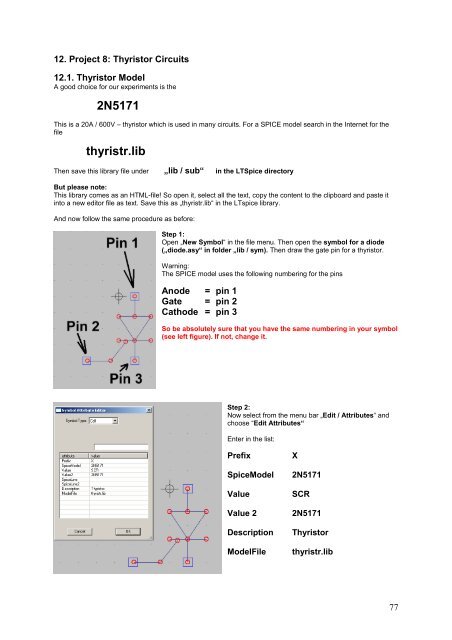
12. Project 8: Thyristor Circuits12.1. Thyristor ModelA good choice for our experiments is the2N5171This is a 20A / 600V – thyristor which is used in many circuits. For a SPICE model search in the Internet for thefilethyristr.libThen save this library file under „lib / sub“ in the LT<strong>Spice</strong> directoryBut please note:This library comes as an HTML-file! So open it, select all the text, copy the content to the clipboard and paste itinto a new editor file as text. Save this as „thyristr.lib“ in the <strong>LTspice</strong> library.And now follow the same procedure as before:Step 1:Open „New Symbol“ in the file menu. Then open the symbol for a diode(„diode.asy“ in folder „lib / sym). Then draw the gate pin for a thyristor.Warning:The SPICE model uses the following numbering for the pinsAnode = pin 1Gate = pin 2Cathode = pin 3So be absolutely sure that you have the same numbering in your symbol(see left figure). If not, change it.Step 2:Now select from the menu bar „Edit / Attributes“ andchoose “Edit Attributes“Enter in the list:Prefix<strong>Spice</strong>ModelValueValue 2DescriptionModelFileX2N5171SCR2N5171Thyristorthyristr.lib77
Step 3:Open „Edit / Attributes“, but now choose „AttributeWindow“. Click on „Value“ in the list and place“SCR“ beside the symbol. Repeat the procedure for„<strong>Spice</strong>Model“. This should be the result.Now the finished symbol must be saved in a newfolder (named „Thyristors“) in „lib / sym“using the name 2N5171.asy“.--------------------------------------------------------------------------------------------------------------------------------------12.2. Switching Resistive LoadsDescription:A sine wave source V1 (peak value = 325 V, frequency = 50Hz) feeds a series connection of a resistor R1 (100) and the thyristor 2N5171. Between the gate and the source a resistor R2 (1k) is added to the schematic. Apulse source V2 is connected to the gate of the thyristor using a “current limiting resistor R3 with 10”.Explanation of other entries on the schematic::a) „.tran 100m“ gives a simulation time from 0.....100ms.b) „.include thyristr.lib“ prepares for the usage of the library with the thyristor SPICE-Models.c) The pulse voltage at the gate is programmed by the line:PULSE (0V 4V 5ms 0.1us 0.1us 10us 20ms)This gives a minimum amplitude of 0V and a maximum amplitude of +4V. The start delay time is 5ms, therise and fall times are 100ns. Pulse length is 10µs with a period of 20ms.78
12.4. Circuit with Gate TransformerVery often practical circuits need complete isolation between the load circuit and the gate circuit. So in this case agate transformer can be used to fire the thyristor:Some details:a) The pulse source to trigger the thyristor is now isolated from the gate by the transformer. But SPICEdoes not accept „floating circuits or nodes“. So resistor R4 (1MEG) has been added to make thenecessary ground connection.b) Also the properties of the pulse voltage must be changed because a transformer cannot transfer DCvalues from the primary to the secondary winding. So we use “-5V” and “+5V” as minimum andmaximum amplitudes.c) Never connect an inductor without a series resistor to a voltage source……so R5 was added to theprimary winding of the transformer.d) The transformer is our well-known part „xformer_01“ of the rectifier experiments.80
To calculate the properties of the line you cut it in pieces -- but you must take very short pieces to simulate the“distributed capacitors andinductors”.Additionally you have to takeinto account the losses of theinductors (...caused by the skineffect which increases withfrequency..) as series resistors.The losses of the insulationmedium are representated byparallel resistors.As soon as a signal is applied to the input of the line, the following effects can the observed:So you can extend the simpleschematic model for a longerline by repeating the circuit.a) At the first instance of time the generator sees the cable simply as a resistive load with a value of the„characteristic cable impedance”, i.e. 50. The applied voltage at the cable input enters the cable and starts totravel along it (= “incident wave”). This characteristic cable impedance can be calculated as follows:Z =InductanceCapacitanceThe inductance and capacitance values always refer to a defined cable length (mostly: 1m). For the well knownRG58-type you have values of100pF / 1m,250nH / 1mb) When the input signal is travelling along the cable length, the small capacitors are charged or dischargedthrough small series inductors. This takes a finite time and so this gives rise to „cable velocity“ or “wavevelocity which is slower than the „ velocity of light in air“.We get:vvcable=lightrFor a coaxial cable ε r (....in America sometimes: „k“) is the dielectric constant for the cables insulation betweeninner and outer conductor.RG58 with Z = 50 Ohmuses polyethylene for thispurpose. If you look at thetable you can see that thewave velocity is reduced to66.6% of the velocity oflight, “C”.c) But what happens to the travelling energy on the cable? (see following chapter).82
13.2. Echoes (= Reflections)At high frequencies it is difficult to measure currents with high precision. Also, the determination of a sourceresistance (by “Open Loop” and “Short Circuit” Measurements) is nearly impossible. So we have to change ourthinking at frequencies higher than 1MHz.Everywhere in a system we use the same „system impedance“ (75Ω for radio and TV and video, but 50Ωin all other applications). This value is valid for the input- and output Impedance of all used blocks, for thecable impedance and for all terminations in the system.The reason is very simple: now everywhere in the system you getperfect power matching (Ri = Ra).With “directional couplers” the differences between ideal and practical situation can be measured and expressedasReflection coefficients.Let us have a look at a pratical example:A pulse voltage source with a source resistance Rs = 50 is connected to a transmission line (coaxial cableRG58 with Z = 50) and generates a short pulse which is sent to the termination resistor Rload at the end of thecable.Now the following happens:a) When the cable is very long and the pulse is very short, then the source does not sense the load at the end ofthe cable. (....You know: the speed of light is 30cm per Nanosecond in the air and 20cm per Nanosecond in aRG58 cable).b) So the cable’s input resistance is 50Ω and forms a voltage divider with the source resistance of 50Ω. Thisgives power matching and a pulse with amplitude of U0 / 2 enters the cable. The associated power (P = Uo xUo / 4 x 50Ω) starts to travel at cable speed to the load resistance. This power is called “incident wave”c) When the incident wave arrives at the load, then it can only be absorbed totally if the load resistor has also avalue of 50Ω. Any difference from 50Ω causes a mismatch of „perfect power matching“ and so the „powersurplus“ is reflected and runs back to source (..at cable speed) as “reflected wave”83
For the exact description of these effects the reflection coefficient „r“ was introduced:Ur =UreflectedincidentZ=ZLoadLoad− Z+ ZNow the reflected wave can be calculated asU= r •reflectedU incidentThe voltage U Load at the load resistor is then:U = U + ULoadincidentreflectedNote:At every point in the cable Ohm’s law must be valid, because you have travelling energies. So you can calculatethe associated current at any point:IUincidentincident= andZIreflected =UreflectedExample:A pulse generator (Rs = 50Ω) generates in „no load condition“ a pulse amplitude of +20V with a pulse width of10ns. The pulse repetition frequency is 1kHz. The generator is connected to a RG58-coaxial cable (Z = 50Ω,length = 100m). The cable is terminated by a 75Ω-resistor. The dielectric constant of the cable is er = 2.25.Calculate and draw the signalsa) At cable’s input b) at cable’s centre c) at cable’s endZSolution:Zr =Z−Z75 − 50=+ Z 75 + 50Loada) Calculation of the reflection coefficient: = + 0.2Loadb) Cable velocity:vCable=cr=83 • 10 m= 2 • 102.25 • s8ms84
100m • sCable−6c) Signal runtime for 100m of cable length: trun= = = 0.5 • 10 s8vCable 2 • 10 ml20V2Sourced) Amplitude of incident wave: Uincident = = = 10VU2e) Amplitude of reflected wave: Ureflected = r • Uincident= 0.2 • 10V = 2Vf) Amplitude of load voltage: ULoad = Uincident+ Ureflected= 10V + 2V = 12VAt the cable input we see at firstthe incident wave (produced bythe pulse generator) with anAmplitude of +10V.After twice the signal runtimefor 100m (= 1 Microsecond)the reflected wave comes backfrom the load and reaches thecable input.After 0.25 microseconds theincident wave reaches thecentre of the cable (= 50m).The echo from the outputcomes 0.5 microseconds laterand passes the centre whentravelling back to the cableinput.Exactly after 0.5 microsecondsthe incident wave reaches theload resistor. Because there isno perfect power match, a partof the arriving energy isreflected and so a reflectedwave is generated. At the loadresistor we measure the sum ofincident and reflected wave =10V + 2V =12V.--------------------------------------------------------------------------------------------------------------------------------------85
13.3. <strong>Simulation</strong> of this Example with <strong>LTspice</strong>We start with the voltage source from the part library. After placing the symbol on the screen we enter theproperties to get a pulse voltage with a source voltage of 20V, a rise and fall time of 0.01ns, a pulse lengthof 10ns and a period time of 1 ms. The source resistance must be set to 50:Note:For such a short rise and fall time of 10picoseconds it is necessary to use amaximum step size of 100 picoseconds inthe simulation settings!Now we need the transmission line „tline“ from the part library. But we must enter the “signal delay time” in theproperties instead of the cable length!This delay time can be calculated with the mechanical cable length of 100m and the “cable signal velocity” of200 000 km / sec as follows:86
tdelayl=vcable100m• s= = 0,5μs82 • 10 mThis delay time of 0.5µs is realized by using two equal pieces of RG58-cable which are connected in series. Eachpiece produces a delay of 0.25µs and so we get again a total delay of 0.5µs as desired. But now it is possible toview the signals in the MIDDLE of the total cable length.We terminate the end of the cable bya 75 resistor and simulate a run timeof 2ms (…please check all of theschematic before starting thesimulation…):After the simulation the three voltages (input, middle and output) are presented in three different diagrams.Compare the result with chapter 13.3.:87
13.4. Open or Short Circuit at Cable’s EndThis is a very simple task because it is only necessary to change the value of the termination resistance.a) Short Circuit at cable’s end:Choose a realistic value of 0.001 (= 1 milli-Ohm) astermination.Then you can watch the following signals.Explanation:At the short circuit (at cable’s end) the voltage must be zero. This means that no power is delivered into this shortcircuit and the incident wave (= power travelling from the source to the load along the cable) is sent back to thegenerator. But to produce zero volts at the short circuit the “reflected wave” (= voltage and power which run back)must change its polarity and so we see a negative echo on the cable.Because we have replaced the ideal short circuit by a 0.001 - termination we get a short pulse with an amplitudeof 400 microvolts at the output of the cable.88
) Open circuit at cable’s endChange the termination to 10M -- this will do foran ideal open circuit.Warning:Never delete the termination R2 from theschematic to get an ideal open circuit. For theprogram this would be a “floating node” and atonce you get an error message and a simulationabort!And this is what you get as a simulation result:Note:Because at the cable’s end the current is zero no power is delivered to the termination. So the incident wave isreflected and runs back to the generator. But now -- as always when a power supply doesn’t have a load -- thevoltage at cable’s end rises to the value of the unloaded source voltage (= 20V in our example).89
13.5. Lossy Cables (i. e. RG58 / 50)13.5.1. How can I simulate an RG58 Coaxial Cable?We need a part from the <strong>LTspice</strong> – part - library which is namedltline(= lossy transmission line).But there is a little problem:We have to write a special model file with the RG58 properties. These properties can be found in theinternet and must be applied to create the desired cable model and symbol.In the <strong>LTspice</strong> manual you will find the necessary information which is as follows:.model RG58 LTRA(len=100 R=1.5 L=250n C=100p)Details:„model“„RG58“„LTRA“„len=100“„R=1.5“is the SPICE syntax for a part modelis the name of the new partmeans „lossy transmission line“means the „unit length” and „len = 100“ says that we have a cable length of 100m if the unit is“1m”.means that for 1 unit length ( = 1m) a series resistance of 1.5 must be taken into account.„L=250n“ gives an inductance of 250nH per unit length (here: for 1m)„C=100pF“ gives a capacitance of 100pF per unit length (here: for 1m)Write this line with an editor and save it as „RG58.mod“ using the path „<strong>LTspice</strong>IV / lib / sub“.(The properties „100pF per 1m“ and „250nH per 1m“ come from the internet for RG58.The value for the losses with „1,5 per 1m“ is estimated and will be checked in the next chapter……90
----------------------------------------------------------------------------------------------------------------------------------------------93
13.5.3. Feeding the RG58-Cables’s Entry with a Pulse VoltageWe now test our „lossy line“ with a pulse voltage at the input. Let the source properties be:Source Voltage Maximum ValueSource voltage Minimum ValuePulse LengthRise TimeFall TimePeriode Time= 20V= 0V= 10ns= 0,01ns= 0,01ns= 1msSchematic:<strong>Simulation</strong> Result:Because the value „R = 1.7 / 1m“ does not change with frequency in the simulation (in comparison with thereality: really a pity!), all harmonics are attenuated by the same factor. So the curve form does not change as inpractice (= no linear distortion). Only the amplitude at the cable’s output is reduced.94
S12 is then the „reverse transmission coefficient“. In this case we terminate the input (Port 1) by 50Ω anddisconnect the input signal generator. The signal generator is now connected to the output (port 2) to measure thefeedback effects at the input (port 1).baS12=1for a 1 = zero2-----------------------------------------------------------------------------------------------------------Output side = port 2:One signal generator is connected to the output (port 2) and sends the wave a2 to this port. The other signalgenerator feeds the Input of the Twoport.With a directional coupler we can at the output separate the incident wave a2 and the “echo b2” coming back fromthe TWOPORTs output:b2 = a1• S21 + a2 • S22If we now disconnect the signal generator from the input and terminate with 50Ω, then the output’s echo consistsonly of the „reflected wave “a 2 x S22” (if the output impedance differs from 50Ω). So S22 is simply the „outputreflection coefficient for perfect matching at the input (= port 1)”.b2S22= for a 1 = zero.a2Now let us look at the rest of the formula:If the input signal generator is switched ON and the output signal generator disconnected and replaced by aperfect 50Ω-Match, we get only the waveb 2 = a 1 x S21at the output. So S21 = forward transmission coefficient means simply the gain or attenuation of a TWOPORT(with perfect match at the output)!b2S21= for a 2 = zero.a1Please remember:The S-Parameters are „wave“ ratios -- that means: voltage ratios. So if you want to calculate the power gain,you must use (S21) 2-------------------------------------------------------------------------------------------------------------------------------------------------------How can we get an input or output impedance value from S11 resp. S22?Use the following formulae, but remember: normally all the numbers are complex……:Input resistance:Z Input1+S11= Z •1−S11Output resistance:Z Output1+S22= Z •1−S22It is also possible to calculate the reflection-S-parameters from measured impedance values, but therefore youneed a modern microwave CAD-program (like the free ANSOFT DESIGNER SV) to save lot of efforts and sweat.And lastly let us have a look at the S-Parameter-file of a modern MMIC (= “Touchstone” or “S2P” file),downloaded from the Internet:97
!.....INA-03184....S-Parameters! Id = 10 mA LAST UPDATED 07-22-92# ghz S ma r 500.0 .32 180 19.2 0 .014 0 .55 00.05 .32 179 19.14 -3 .014 3 .55 00.10 .32 176 19.05 -7 .014 4 .57 -30.20 .32 172 19.05 -14 .014 6 .55 -50.40 .32 165 18.78 -29 .014 10 .53 -110.60 .32 158 18.71 -43 .015 11 .51 -140.80 .32 151 18.53 -57 .015 13 .51 -171.00 .32 144 18.18 -72 .016 21 .50 -201.20 .30 135 18.27 -86 .016 25 .50 -231.40 .31 126 18.10 -102 .017 30 .49 -291.60 .30 117 17.92 -117 .018 38 .48 -341.80 .26 102 17.49 -135 .019 44 .45 -412.00 .22 92 16.62 -153 .020 49 .40 -502.50 .09 91 12.88 168 .021 57 .26 -483.00 .14 160 8.79 134 .023 65 .22 -333.50 .24 151 5.92 108 .025 69 .26 -334.00 .29 139 4.18 87 .029 81 .28 -43And this is how to interprete these files:a) A line starting with an exclamation mark is a comment and therefore ignored for calculationb) The line # ghz S ma r 50“ means:The first value is the measuring frequency in GHz.Then follow the 4 S-parameters in the range S11 S21 S12 S22“ma” says: every S-parameter is given as its magnitude, followed by the angle.“r 50” tells us that the system resistance (for measurement and application) is real 50 Ohm.Example line for f = 1GHz:S11 = 0.32 / 144 degrees (Magnitude of the input echo is 0.32 x a1, the phase of the echo is 144 degrees -- caused by an input impedance not equal to 50 ).S21 = 18.18 / -72 degrees When the output (= Port 2) is terminated by 50, then we get a voltage gainof 18.18 (= ratio of output wave a2 referred to input incident wave a1)S12 = 0,016 / 21 degreesThe feedback voltage measured at the input (= port 1) is 0.016 =1.6% of theoutput wave a2S22 = 0.5 / -20 degrees Magnitude of the output echo is 0.5 x a2, phase of the echo is 20 degrees --caused by an output Impedance not equal to 50----------------------------------------------------------------------------------------------------98
14.2. Example: 110MHz – Tchebyshev Lowpass Filter (LPF)Let us now simulate the S-parameters of a 110MHz Tchebyshev lowpass filter. This type of filter suffers from“passband ripple” but provides a sharper transition from the passband to the stopband.Properties:„Ripple“ corner frequencyfc = 110 MHzFilter degree n = 5System resistanceZ = 50„Passband ripple“0.1 dB.(This ripple causes a maximum value of S11 = -16,4 dB)For the filter part calculationsuse the free microwave CADsoftware (Ansoft DesignerSV) with the integrated filterdesigner and you get:C1 = C3 =C2 =L1 = L2 =33.2 pF57.2 pF99.2 nHAnd this is the simulation schematic for <strong>LTspice</strong>:99
Explanations:a) The directive .net I(R1) V1 starts a network calculation with theoutput voltage referred to the input voltage (given by source V1).b) Then program a decadic sweep from 1Hz to 300 MHz with 101 points per decade by the directive.ac dec 101 1 300MEGc) For a sweep the properties of source V1 must be set to „AC amplitude =1 and AC phase = 0“:AC 1 0.d) After a right mouseclick on the symbol of source V1 enter the value for the necessary source resistanceof 50 in the system:(Rser=50)Now press the simulation button and follow these steps:Step 1:The diagram for the results is still empty. So click right on it with your mouse andchoose„Add Trace“Step 2:Find„S11(v1)“in the list, mark it andpress OK.For professionals:In this list also the Y-and Z-parameters canbe found...100
Step 3:The result is not so bad, but the presentation…….The phase curve might be interesting, but we want to delete it. The dB-scaling of the vertical axis must beimproved.So move the cursor to the scaling of the right vertical axis and click on it. Choose in the menuDon’t plot phase.The phase curve disappears at once.Now we repeat this procedure with theleft vertical axis and enter the valuesof the left figure (= range from 0dB to -50dB with a tick of 10dB).At last and once more click right on the diagram to activate the optionGRIDNow you have this result:Step 4:We complete the work by adding the S21 curve. Let’s go:Right mouseclick on the diagram / Add Trace / choose S21 and press OK.Sorry, but it is now better to repeat the procedure with the scaling of the left vertical axis to show a range from0....-50dB. This gives the final result on the next page.101
For a separate presentation of the two S-parameters right click on the diagram and chooseAdd Plot Planefor the parameter S21. Delete the S21-curve in the „old“ diagram and scale both diagrams again:102
15. Project 11: Double Balanced Mixer (= DBM = Ring Modulator)15.1. Fundamentals and DefinitionsThis well known circuit is used for converting frequencies without changing the information contents.We have two inputs and one output:Note:a) RF = radio frequency input. Here the applied signal amplitude must be small (typically below50...100mV)b) LO = local oscillator input. Here the signal must be high (typically up to several volts)c) IF = intermediate frequency output. Here we find the converted signals.This operates a multiplier circuit for the two input signals!When two sine signals are multiplied we get the following result:sin12( α )• sin( β ) = [ sin( α + β ) + sin( α − β )]This means for our circuit:At the output of the DBM the two input signals have disappeared and are now replaced by their sumfrequency and difference frequency!When using a square wave signal as the LO-input, then this signal consists of the fundamental frequency f1 andthe harmonics (with 3 x f1 , 5 x f1 , 7 x f1 , 9 x f1......).Not only the fundamental frequency but also the harmonics are now multiplied by the RF-signal in the DBM andproduce sum and difference frequencies with amplitudes that decrease linearly with the “harmonic’s degree”.So you get at the DBM’s output a lot of „signal pairs“ (= sum- and difference frequencies). Every pair islocated at a harmonic frequency.In practical applications the desired new frequencies must now be picked out with a lowpass or a bandpass filterby the user.103
15.2. The Ring ModulatorThis part is used everywhere in communication systems and is offered by a lot of manufacturers -- as an active orpassive device. We’ll examine the standard passive version.A ring of four schottky diodes isconnected to two transformers.Each transformer uses 3 identicalwindings. The two secondarywindings are connected in series.The use of superfast schottkyswitching diodes and specialmicrostrip circuits enables cutofffrequencies higher than50....100GHz in specialapplications.Explanation:„LO-IN“ means „local oscillator input” for the converting signal.„RF-IN“ means „radio frequency input” for the information which shall be converted.„IF-OUT“ means „intermediate frequency output” and delivers the multiplication result.Principle of operation:The LO-signal at the secondary winding of the left transformer (amplitude: up to several volts….)switches the right diode pair ON at the positive halfwave and the left diode pair ON at the negativehalfwave.So either the upper secondary winding or the lower secondary winding of the right transformerwith the RF signal is connected to the IF output by the conducting diode pair. But the RF signal whichfinally reaches IF-OUT is changing its polarity rhythmic with the LO frequency. That is the same effect asmultiplying the RF – sinewave with a LO-squarewave (amplitude values: +1 and -1).Advantages: Very low distortion. Useful for broadband applications up to many GHz. Needs no power supply, butcorrect 50-matching at all ports. Produced in huge quantities at reasonable prices by a lot of manufacturers.Disadvantages: Due to the missing power supply the complete „switching energy“ must be delivered by the LOsignal source. It demands high LO levels for rapid diode-switching and low distortion. There is no gain but alwaysan attenuation of 5….8dB between the RF input and the IF output. This increases the noise figure in a system andthe attenuation must be compensated by more „pre-amplifying“.104
15.3. The necessary TransformersThe „weak points“ of this circuit are always the 2 broadband transformers …and the special construction is a topsecret guarded by the manufacturers! The transformers will in any case limit the bandwidth and the upperfrequency.So let us study an example with LO frequency = 1MHz and RF frequency = 100kHz. The lower cutoff frequencyof the transformer should therefore be below 100kHz and the upper frequency limit min.10….20 MHz.We use our well known „xformer_02“ with 3 identical windings and vary the properties to reach thesespecifications.But remember: when the mixer is operating, always only one of the two secondary windings is in action, while theother is “idling” as long as the active diode pair is switched ON! So in the transformer simulation only onesecondary winding is terminated by 50 while the other winding is simply feeding a 10M-Resistor. This avoidsthe error message “node is hanging free”.The main winding inductance is 100µH, copper resistance is 1 and winding capacitance is 1pF:Now let’s tackle the complete mixer!105
15.4. DBM <strong>Simulation</strong> with ideal TransformersFrom the left comes the LO signal to switch ON and OFF the Schottky diodes (sine wave, peak value = 2V,frequency = 1MHz). From the right comes the information as RF signal (sine wave, peak value = 20mV, frequency= 100kHz.Both ideal transformers use 3 separate windings(each L= 10mH) which are magnetically coupled. The couplingfactor is 1 (= 100%).The Schottky diode comes from the <strong>LTspice</strong> part library. The symbol is named “schottky”.A simulation time of 1ms gives a frequency resolution of 1/1ms = 1000Hz. So for a number of 100 000 truesamples a maximum time step of 1ms / 100 000 = 10ns must be used. This time step corresponds to a minimumsample frequency of 1/10ns = 100MHz and so no aliasing effect should be found up to a signal frequency of50MHz.Data compression is switched OFF by the spice directive.options plotwinsize=0.This is the screen before starting the simulation:And so the screen looks like this after the simulation of the output voltage at resistor R2 and zooming106
The polarity changing of the RF signal (caused by the LO signal) can clearly be seen. But: the „ON“ voltage of0.3V of every Schottky diode causes distortion at every zero crossing.Lastly let us look at the FFT result for the output voltage. So right click on the time domain curve, open “View” and“FFT” and use 65536 samples in time.Press OK and modify the scaling of the diagram axis:Frequency axis:linear ; start frequency = 0Hz ; stop frequency = 10MHz ; tick = 1MHzVertical axis:dB scaling from -40dB …..-120dB with a tick of 10dB.Here comes the confirmation of theory:At every LO harmonic frequency (3MHz ; 5MHz ; 7MHz ; 9 MHz…) we find a signal pair consisting of the sum andthe difference frequeny of the RF signal and the harmonic.Neither the RF signal nor the LO signal nor the LO harmonics should be found at the output.107
16. Project 12: <strong>Simulation</strong>s with Digital Circuits16. 1. What you should know before you beginSorry, but this information is not described in the online help or the included examples. So you need to gain someof your own experience (..also gained through the use of other SPICE-programs) by exploring the problems andto master these non-intuitive constraints .The most important rules for the „normal user“ are:The included library „[Digital]“ contains only „ideal fundamental blocks“.Each of them always has 8 pins!The reason for this is:a) You always have several input pins (e.g. an AND-Gate has 5). Please leave all non-used pins opencircuit(unconnected). They will be ignored for the simulation.b) Normally you will get not only the desired output signal but also the inverted signal.c) Logical levels are „0 Volt“ for „Logical Zero” and „+1 Volt“ for „Logical 1“. The internal thresholdvoltage is 0.5V.If you need to work with other voltage levels (like TTL = 0V /+5V), thenright click on the part symbol, open the line „value“ and write thefollowing entry:Vhigh=5V Vlow=0Vd) Output pins should not be hanging free in the air. So please add a label or terminate them by a10k – resistor to ground for a troublefree simulation.e) The supply voltage pins are completely missing….you are working with “ideal parts“.Use the „PULSE-“ or the PWL voltage as input signal.Minimum value is 0 Volt, maximum Value is = +1Volt (…other values are handled as discussed above…)As rise and fall time use 1ns.To see your simulation results open separate diagrams by right clicking on the result screen and choosingAdd Plot PlaneUse as many separate diagrams as you need to present signals -- otherwise you go crazy after a short time.Filling such a plot pane is very simple: click right on the diagram and choose “Add Trace”.108
16.2. Simple start: the Inverter (= NOT)Get the part as „Digital / INV“ from the part library and use as the input signal a symmetric pulse voltage (Umin =0V / Umax = +1V / Rise Time = Fall Time = 1ns / Pulse Length = 500µs / Period Time = 1ms). Simulate for 5ms.Connect the Voltage Source to the upper input pin and leave the other input pin open-circuit.Now simulate, open two diagrams by using „Add Plot Plane“ and view the input and the output voltage. You willget the following screen when selecting „Tile vertically“ in the „Window“ menu:109
16.3. AND- and NAND GateLet us simulate an AND Gate with 2 inputs. One input is fed by a symmetric pulse signal of 1kHz, the other inputwith a symmetric pulse signal of 5kHz. Simulate for 5ms.As already mentioned, leave all unused input pins open-circuit and use a label for the output pin.Here is the simulation result:110
16.4. D FlipflopThis is the well known „Binary Divide by Two Frequency Divider“. At the output you get one half of the input clockfrequency. The inverted Q-output is connected to the D-input pin.„Preset“ and „Clear“ must not be active and so they are connected to ground.111
16.5. Three Stage Frequency Divider with D flipflopsThis is a very simple task because you only have to connect three D-stages in series and wire them.<strong>Simulation</strong> time is 20ms, the input clock is a square wave of 1kHz.If anyone has noticed that this chapter is short in comparison to the others: you are right. The reason is simple: inthe LT<strong>Spice</strong> library the complete TTL and CMOS part collection is missing. This is really a pity when you considerthat all these interesting circuits and schematics and problems could be simulated.But there is a way -- this link:http://tech.groups.yahoo.com/group/LT<strong>Spice</strong>/files/%20Lib/Digital%2074HCTxxx/It’s the address of the LT<strong>Spice</strong> usergroup and there you find all the missing parts and symbols of the 74xxfamilies.Thanks to Helmut Sennewald who has done the work of creating these important parts. Once more: Thanks,Helmut, for all your personal effort!But:This is a community and so you have to register first to get your ID and password. (no problem, it is free). If youdo this you will be astonished and pleased: you’ll find extensive Online discussion consisting of calls for help,questions, answers, remarks, advice, offers, problem solutions....and a lot of nice and kind people, always readyand willing to help.So why wait? Go and see.112
17. Project 13: Noise <strong>Simulation</strong>17.1. FundamentalsPlease noteThe following 3 chapters are part of my article„Practical Project: Noise factor measurement with older SpectrumAnalysers, <strong>Part</strong> 1 and 2“.Published in „VHF –Communications”, Issues 2008-Q1 and 2008-Q317.1.1. „Noise“ -- where does it come from?That can be answered very quickly and precisely: in each electrical resistance where a current flows andelectrons move, there exists noise. As soon as heat comes into play (that is always the case above absolutezero), electrons have an independent existence. They move ever more randomly and not directly from minus toplus. They collide, rebound, are hurled forward or off to the side….. This makes the current vary irregularely bysmall amounts due to the influence of heat. This effect is called thermal noise. Even if no outside voltage isapplied these independent movements of the charge carriers, due to heat, develop a small open circuit voltageV noise. This can be computed as follows:Vnoise=4hfBRehfkT− 1Whereh = Planck’s constantk = Boltzmann’s constant = 1,38 x 10 -23 J / KelvinT = absolute temperature in KelvinB = bandwidth in Hzf = center frequency of the band in HzR = resistance value in This seems terribly complicated and not practical, but the following simplification can be used without problem toat last 100GHz and temperatures down to 100K:V NOISE=4kTBRChanging this formula around it suddenly looks much simpler: V 2RNOISE2= kTBa) This is a simple indication of power! Each resistance, independent of its resistance value, produces an„Available Noise Power“ proportional to kTB.b) The resistance should be regarded as voltage source consisting of V NOISE and a noise free internalresistance R to generate the noise power. A noise free load resistance with the same value R isconnected to this source. Because voltage across the load resistance is then half V NOISE the loadresistance receives the Available Noise Power kTB.c) This noise power increases linearly with the absolute temperature of the circuit and the voltage with thesquare root of the power. The spectral power density (power per Hz) is independent of the frequency.This is called “White Noise”.113
Important:Receiver systems are nearly always specified in terms of „power levels“ instead of voltages. These arelogarithmic measurements so that the gain can be calculated by adding levels instead of multiplication. The mostfamiliar unit is “dBm” -- that is not a voltage but a power rating in relation to the system reference resistance:ThusP 0 = 1 milliwatt at the system resistancePower level in dBm = 10log (power value / 1mW)If the noise power “kTB” is considered in more detail, an interesting simplification can be introduced:kTB = (kT) x B = (Noise Power Densitiy) x (Bandwidth)The Noise Power Density „kT“ represents the power in every Hz; this must be multiplied by the bandwidth in orderto calculate the noise power produced. Converting this to a power level calculation the following formula shouldbe committed to memory:Each resistance produces at ambient temperature (T 0 = 290K) an available noise level and thus anavailable noise power density of-174dBm per Hz of bandwidthFor a bandwidth larger than 1 Hz:Available noise power level in dBm = -174dBm + 10log(bandwidth in Hz)As a simple example:The no load noise voltage V NOISE at the terminals of a 50 resistor for a bandwidth of 100kHz will be calculated:Noise level with matching = -174dBm + 10log(100000) = -174dBm + 50dB = -124dBmThat results in an available noise power ofP = 1mW • 10−12410= 1mW • 10−12,4= 4 • 10−16WThat will produce a voltage across the 50 resistor of:−16VNOISE = P • R = 50 • 4 • 10 W = 141nVSo the open circuit voltage is twice this value, thus 282nV.114
17.1.2. Other Sources of NoiseEach active component (valve, bipolar transistor, barrier layer FET, MOSFET, HEMT, etc.) produces twoadditional types of noise:a) Shot-Noise is produced in valve diodes and PN transitions by distortions of the current flow whencrossing potential differences . It produces wide band, white noise.b) Flicker-Noise or „1 / f – Noise“ (= sparkling noise) results from defects in the crystal structure caused byimpurities. They lead to short pulse type fluctuations in the current flow that produce a spectrum whosepower density decreases with rising frequency. There exists a corner frequency and it is interesting tosee how this differs between active components. The following figure is a good representation. Thereference material in the homepage of Mohr <strong>Associates</strong> should be obtained from the Internet. It containsa precise but compact introduction to the subject.Before semiconductors, gas discharge tubes were used as sources of noise, they produced a very wide bandplasma noise.The following section shows how the different kinds of noise in a circuit can be considered and how they can besummarized by only one parameter.115
17.1.3. Noise Temperature and Noise Factor for a Twoport SystemWhen components of a communicatons system are specified they usually have the same system resistance(normally 50, but for radio, television and video systems it is 75) and signal quality information required forcorrect transmission. This is often expressed by the SINAD value (= Signal to Noise and Distortion). Themaximum signal level is limited by over modulation, distortion, intermodulation etc. The “noise floor” (in addition,other disturbances e.g. cross modulation from other channels) gives the minimum signal level in the system.Therefore each component must be specified by its S-Parameters as well as its noise behaviour.When referring to noise, the following terms are usually evaluated (unfortunately not all authors use the sameterminology):a) The „equivalent noise temperature T e “ of a component expresses the self-noise ofthe component by an additional temperature rise for the noise source resistance. The component itself isthought of as noise free.b) The „NOISE FIGURE (NF)“ indicates, in dB, how much worse the signal-to-noise ratiobecomes after the signal has passed through the component.c) The „NOISE FACTOR (F)“ is like the Noise Figure as above, BUT NOT IN dB, only as asimple power relationship.-----------------------------------------------------------------------------------------------------------------17.2. <strong>Simulation</strong> of the Spectral Noise DensityThis sounds complicated, but isn’t. In the introduction we stated that every resistor delivers at his terminals anAvailable Noise Power of:kTB = (kT) x B = (Noise Power Densitiy) x (Bandwidth)The noise power densitiy is the power which can be measured in every Hz of the bandwidth. You get the totalavailable power if you multiply this density by the valid bandwidth (…or by integration over the bandwidth if thenoise power density varies with the bandwidth).But very often one prefers to handle the voltage instead of the power -- because it is easier to measurevoltages at different frequencies than power. So use the well known equation to jump between these twovalues:2VoltagePower =Resistanceby using the known system resistance „R“.When You now calculate the square root of the Noise Power Density, you’ll get an expression for the „SpectralNoise Voltage Density”, usually given inNanovoltsHzIf you multiply this result with the factorBandwidthyou’ll get the total noise voltage.Let use consider the included example „NoiseFigure.asc“ of the software -- you find it in the „Edudational“ folderand it is a one stage transistor audio amplifier, which we will modify a little bit for our purposes.116
At the output we addthe label „out“ for thenoise simulation.Use the path„<strong>Simulation</strong> /Edit <strong>Simulation</strong>Command /Noise“ to edit thenecessary simulationcommand:.noise V(out)V1 dec 1011k 100kThis means:Simulate the spectral noise voltage density at the label „out“ and refer it tovoltage source V1 with internal resistor R6 = 1k.Use a decadic sweep with 101 points per decade from 1kHz to 100kHz.And this is the result for the output noise voltage density V(onoise) when clicking with the „cursor probe“ on theoutput pin:Please examine the scale and the units of the vertical axis....117
No problem, now to show the noise voltage density V(inoise), referred tothe input!This is a voltage source which can be thought in series to the noise free sourceV1. So right click on the diagram, choose „Add Trace“ and then „V(inoise)“ inthe list (see left figure).If you examine the list then you‘ll find that not only V(inoise) can be shown butalso V(onoise) and the gain.This is the input noise voltage density V(inoise) …..…and this is the gain versus frequency:118
17.3. <strong>Simulation</strong> of the Noise Figure NF (in dB)In communications systems many blocks are connected in series. So the reduction in signal quality in every„twoport“ caused by noise must be known and is expressed by theNoise Figure NF in dBSo the „NOISE FIGURE (NF)“ ist the difference in db between the signal to noise ratio at the input and theoutput of the twoport.For a noise free twoport the signal to noise ratio is identic at input and output pin and NF = 0dB(Please note:The input signal source V1 delivers not only the desired communication signal to the twoport but also noise due tothe internal resistance of the source. So if only this noise is amplified by the same factor as the communicatonsignal, the signal to noise ratio at the output would stay the same as at the input. But because the block addsnoise itself....)If you change the NF-value in dB to a linear ratio, then you get the „noise factor F“.Now let us tackle the NF-simulation with LT<strong>Spice</strong>, following these steps:a) To get „dB“ at the result, we need the relationshipNF = 10 x log 10 (…..)b) In the brackets we must insert the ratio of the total input noise power (= total output noise power, referedback to the input = P inoise) to the noise power part which comes only from the source resistance (= PSource).If both powers are equal, then we have a noise free twoport and the noise figure NF isNF = 10 x log(1) = 0 dBBut in reality you will always have noise factor values larger than 1 = NFvalueslarger than 0 db....The noise power produced by a resistor increases linearly with the absolute temperature, and T = 290K wasalways the standard value for every noise calculation. But now the global temperature is rising, climate ischanging and so electronic people prefer calculations with T = 300K.Now let us continue with the calculation of the power ratio:PPinoiseSource2 V inoise24 R •Source Vinoise==k • T • B 4 • k • T • B • RSource„k“ is the Boltzmann constant, „T“ is the absolute temperature in Kelvin, „B“ ist he bandwidth of the system,R Source is the internal resistance of the input voltage source.If we consider spectral power density then the bandwidth is automatically 1Hz. Then we can ignore the bandwidth“B” for the calculation and get the final formula which must be converted to a SPICE command:2 Vinoise= 10 • log4 • k • T • RNF in dBSource119
And assuming a actual climate change contribution we use an absolute temperature of 300K:2 Vinoise= 10 • log 4 • k • 300 • RNF in dBSourceProblem:In a simulation with LT<strong>Spice</strong> it is only possible to calculate this formula (and to show the result) by theusage of aPLOT command!So we must write the following line for the calculation of the noise figure NF(1K) with a text editor, when thesource resistor’s value is 1k:.func NF(1k) 10 * log10(V(inoise) * V(inoise) / (4*k*300*1k))Save this line in a new file namedplot.defsand save it in the LT<strong>Spice</strong> program folder.Caution: After saving this file you must close LT<strong>Spice</strong> and start it again. Onlyin this manner the new „plot.defs“ are included and used by the software!The rest is simple:simulate the circuit, clickright on the result diagramand choose„Add Plot Pane“to get an empty diagram.Then click right on thisnew diagram an call„Add Trace“EnterNF(1k)In the empty command lineand press OKThe result is not totally perfect, becausethe „dB“ calibration on the vertical axis is missing and this cannotbe altered ...120
-------------------------------------------------------------------------------------------------------------------------------------------------Task:Communications systems generally use a system resistance of 50. So please repeat the NF simulationfor this value.Step 1:Change the internal resistance of the voltage source V1in the schematic to 50.Step 2:Open the file „plot.defs“ with the text editor and modify the command line to „NF(50)“ as shown in the figure.Do not forget to save this modified file correctly…Caution:Please close <strong>LTspice</strong> now and start it again. Only then the modification isaccepted and used by the software. Otherwise you get a cryptic errormessage…121
Step 3:Simulate again, open a new „Plot Pane“ and then “Add Trace”. Enter “NF(50)” in the line „Expression(s) toadd“ and press OK. This is the result:The vertical axis is now calibrated in „dB“, but this is not indicated….122
18. <strong>Simulation</strong> of a Sine OscillatorLet us have a look at a Colpitts sine oscillator using a collector-grounded NPN – transistor.This is the schematic:Note:To start the (simulated) oscillation the circuit needs a little „push“.This is done by programming a special property of the supplyvoltage:„Rise linearly from 0V to +12V in a rise time of 10microseconds”.We right click on the symbol of the voltage source, choose„Advanced“ and use the PWL-function with the value pairs:0V at t = 0+12V at t = 1usThe „<strong>Simulation</strong> Settings“ are set to „Time domain (Transient)“ andthe simulation time is 0….20ms. This gives a frequencyresolution of 1/20ms = 50Hz in the spectrum. The maximumtime step is set to 100ns, so SPICE doesn’t overlook the startingprocedure described above. . This now gives a number of 20ms /100ns = 200 000 sample for the FFT computation.And the data compression must be switched OFF by the directive.options plotwinsize=0123
Now we need a transistor with the symbol name „npn“ from the part library. Search and place it on the schematic.As soon as you right click on the NPN transistor’s symbol, press the „Pick New Transistor“ button. Then find theBC547B which we want to use for our simulation.Simulate the voltage at the base of the transistor to get this screen:Use the zooming function to show the details of this voltage and to determine the time period for onecycle of the signal. Calculate the oscillating frequency. Examine the curve for distortion.124
The duration of theperiod is 28ms andthis gives a frequencyof 35,7kHz.But the curve is a little“clipped” on one sideand this means thatthe feedback is too“strong”. This can beseen when viewingthe frequencyspectrum of thissignal.So right click on the waveform viewer window and choose „View“, then „FFT“ with 131 072 data points in time.At lastly show the curve with a linear frequency range from 0 to 300 kHz with a tick of 50 kHz:Now we can see the decreasing amplitudes of the harmonics with increasing frequency. Also the “fundamentaloscillating frequency“ can now be determined more accurately as 35.7kHz.But the 2 nd harmonis is only attenuated by less than 20dB and this is caused by the unsymmetry of the signal(Remember: in a really symmetric signal you don’t find any even harmonics….).So any distortion of the symmetry can at once be recognized by testing for even harmonics in the spectrum.125
Note:Resistor R4 / 680Ω gives the positive feedback which causes the oscillation. A part of the emitter AC current isflowing into the resonant circuit through this resistor and „compensates the losses“.So if you increase the resistor’s value, the positive feedback will get weaker and weaker. This gives less distortionbut the oscillation will suddenly stop.Task:Try to find out this stop point by increasing the value of R4 and repeating the simulation.Watch the improvement of the waveform and check the better attenuation of the harmonics by the FFT-simulationof the frequency spectrum..Also be aware of the „oscillation start delay“ when reducing the feedback. When approaching the criticalpoint you get signficantly longer delays before the oscillation starts.(Note: with a resistor value of 6.8k you are not far from this point…please check it!)This is the result for 6.8k. The oscillation start delay is increasing….…but now you geta nearly perfect curve!126
And the FFT spectrum proves this.127
19. Signals and Harmonics19.1. FundamentalsIf you ask anyone what signals are found on power lines all over the world, you’ll always get the same answer: “asine wave with a RMS-value between 110V and 230V and a frequency of 50 or 60Hz, depending of the specificcountry”. But if you continue and ask:“Is that all?”Even specialists may give a wrong answer. OK, there are sometimes harmonics of the line frequency, but muchmore important are the effects caused by switching on or off. So let us look at the correct definition of a signalconsisting of only one frequency:Only a pure continuous sinewave where neither the startpoint nor the stop point canbe observed consists ofonly one spectral line!This means that in every day usage you should always clearly distinguish between “distortions of a signal” and“switching events including changes”.SwitchingEvery switching ON or switching OFF of a signal or increasing or decreasing the amplitude produces a “signalcollection” which travels away (with light velocity) from the point of generation. You know that as a “click” from atransistor radio when switching on the light in a room and you should know that in this moment you get thecomplete frequency range loaded with energy! Very low and low frequencies will travel away using wires, highfrequencies prefer wireless travel. But normally the amplitudes decrease rapidly with frequency when “changing astate very slowly” and so TV and communication are still relatively unaffected.Two examples:Switching On orOFF of a DC voltagegives a spectrumwith decreasingspectral powerdensity at increasingfrequencies.But:Very short pulses(with nearly Diracform) have aconstant powerdensity over thecomplete frequencyrange.So you cannot avoidthis “plop” becausethere are no gaps inthe completefrequency spectrum!Distortions of periodic signals128
Please remember:Every -- even the smallest! -- deviation from the perfect sine wave generates newadditional frequencies!These new frequencies are called “harmonics” and they are multiples of the fundamental frequencyBut there is another axiom:If only one half of the curve is distorted then wespeak of “asymmetric distortion” where you findeven and odd harmonics in the spectrum.This will also happen when the positive and thenegative half is distorted in a different manner.But when you find perfect symmetrical distortion,the spectrum consists only of the fundamentalfrequency and ODD HARMONICS!This means that there are only the lines withf1 / 3 x f1 / 5 x f1 / 7 x f1…Note:If a sine wave’s amplitude, phase or frequencyis varied by another signal, you will also find new frequencies.But this is the mystery of modulation…..On the next page you find a little overview for different waveforms with the signals in the time domain, in thefrequency domain and the formulae to compute the harmonics.129
130
19.2. <strong>Simulation</strong> of a Single Pulse SpectrumNow let us test the statement in the last section and examine the following pulse signal:Umin = 0V ; Umax = 1V ; risetime = falltime = 1µs; pulse width = 1ms.The pulse signal (measured at R1) starts after a „delay time“ of 2ms. The simulation time is 0… 10ms and the„maximum time step“ has a value of 100ns. So we get 10ms/100ns = 100 000 real samples of the simulatedcurve. And the data compression of the result file must be switched off by the directive “.optionsplotwinsize=0”.The signal is generated by a PWL voltage source using the following data:0 Volt at t = 00 Volt at t = 2ms1 Volt at t = 2.001ms1 Volt at t = 3,001 ms0 Volt at t = 3,002 msAfter the simulation of the voltage at R1 open the menu „Window“ and choose the option tile horizontally“. Thisgives this screen.Now we want to perform a Fast Fourier Transformation and so some explanation is necessary:Choosing a simulation time of 10ms is crucial for the FFT simulation result because you get from it thelowest frequency of the spectrum AND the frequency resolution (…including the line width of a signal…)by the following relationship:frequency resolution = 1 / simulation time = 1 / 10ms = 100HzChoosing a “maximum time step” of 100ns during this simulation time of 10ms results in a minimum amount of10ms / 100ns = 100 000 „samples“ which are then saved.131
This is the absolute upper limit for the „number of data point samples in time“ whichmust be entered in the menu when calling and before starting the FFT. So let’s stay onthe safe side and use the preset value of 65536 Samples.If you use more than the mentioned 100 000 samples: this can cause errors and / or an additional noise floor athigh frequencies).But:Increasing the number of produced or used number of samples in a FFT gives a higher stop frequencyand a higher amplitude dynamic range. In other words: a better resolution (and a longer computation timeand a larger data file….)So right click on the waveform viewer, go to „View“ and „FFT“ and set the sample number to 65536. Start the FFTsimulation with OK and afterwards modify the result as follows:a) Move the cursor to the scaling of the vertical axis and left click: now you can change to „linear presentation“b) The horizontal axis set to „linear“, using a start frequency of 0Hz, a stop frequency of 10kHz and a tick of 1kHz.c) Finally choose „tile horizontally“ under „Window“ in the main menu for this result:The simulation result confirms the theory which says:a) In the spectrum of a non-periodic signal you cannot find any discrete frequency lines. The completefrequency range is „loaded“ with energy. So what you see in the diagram is the spectral power density.b) The amplitude of this density follows to a „Sin x / x“ envelope function.c) “Zeros” in the envelope are always found at every multiple of 1 / pulse length(Shortening the pulse length increases the “frequency of the fist zero” and all following)d) The diagram starts with a frequency of 100Hz = 1 / 10ms = 1 / simulation time.The curve is plotted with thick lines. You find this option by selecting the “button with the hammer” and„Waveforms tab“ as „Plot data with thick lines“…132
19.3. <strong>Simulation</strong> of a Periodic Pulse SpectrumWe use the same signal as in the preceding section, but repeat it at 100 times per second. Therefore we need apulse voltage source. In the circuit diagram below you can see how to program the pulse source to achieve this.The simulation time is increased to 50ms (which gives a frequency resolution of 20Hz) and the maximum timestep is set to 100ns. So we get a minimum of 500 000 actual samples and can use a number of 262 144samples for the FFT.Now simulate the voltage at R1 and plot the spectrum. Display the FFT result using the following settings:Vertical axis:Horizontal axis:linearlinear ; start = 0kHz ; tick = 1kHz ; stop = 10kHzYou can see:a) It’s a periodic signal, so we get a pure „line spectrum“ with the fundamental frequency of 100Hz andthe harmonics at every multiple of 100Hz. Due to the simulation time of 50ms the diagram starts at 20Hz.This is also the width of every simulated line.b) A pulse length of 1ms gives a Sinx/x envelope functionc) As before the “zeros” in the envelope can be found atand it’s multiples.F NULL = 1 / pulse length = 1 / 1ms = 1kHz133
19.4. An Ideal Sine WaveLet us proove the definition which we stated in chapter 19.1 (= fundamentals):Only a pure continuous sine wave where neither the start point nor the stop point can beobserved consists of only one spectral line!We use a sine wave with a peak value of 1V and a frequency of 1kHz. <strong>Simulation</strong> time is 60ms using a maximumtime step of 100ns. Thus we get 600 000 samples and so it should be possible to find every undesired signalwhen using 524 288 samples for the FFT. The data compression must also be switched off and the simulation isan integer multiple of the signals’s time period (as recommended in chapter 5, FFT)It is true! From 17Hz up to 4.4MHz every undesired signal is attenuated by more but 160dB and only the 1kHzsine wave line can be seen. Nearly ideal and perfect…134
19.5. The „Asymmetric Clipped“ Sine WaveThis is done by a zener diode in series with a resistor and showing the simulation of the diode voltage. So thepositive half of the sine wave is limited to 0.7V by the conducting silicon diode in the circuit.When polarity is changing we measure -15V due to the Zener voltage of a BZX84C15L.But first you have to pick up the diode symbol from the menu and place it. Then right click on the symbol andopen the menu „Pick new diode“.The peak value of the input sine wave must be increased to 50V. Only then the limiting effect can clearly be seen.<strong>Simulation</strong> time is 0…60ms with a maximum time Step of 100ns. This gives 60ms/100ns = 600 000 samples forthe FFT. Do not forget to switch off the data compression.On a linear scale show the frequency range from 0 to 20 kHz to see the mixture of even and odd harmonics:135
19.6. The Symmetrically Clipped Sine WaveThis is a simple exercise because we connect two BZX84C15L zener diodes in series (opposite polarization).A sine wave is applied again (peak value = 50V, f = 1 kHz). <strong>Simulation</strong> time is 60ms and the maximum time stepis 100ns. This gives 600 000 samples. Data compression is switched off.We use the same scaling as in section 19.5 and now you see that only odd harmonics can be found.136
20. The Secret of the Impulse ResponseIn modern system theory, remote control and communications the Laplace- and Fourier- and Fast FourierTransformations are very important tools.But before starting with an application you have to know the transfer function of the system, which is the ratio ofoutput voltage to the input voltage for all frequencies in complex form (= magnitude and phase).f you know this “transfer function” then it is possible to predict the “system’s response “ for any inputwaveform using two different methods.====================================================================================Method 1 / frequency domain:Multiply the spectrum of the input signal with the transfer function spectrum and you get the spectrum ofthe output signal.Then the inverse Fourier transform will give you the response of the output signal in the time domain.====================================================================================In a complicated system , sometimes the exact calculation or measurement of the transfer function as „magnitudeand phase for different frequencies“ is difficult or impossible to determine. In these cases use the following:If the input to an unknown system is a „Dirac - Impulse“, then the output of the system has all theinformation about the transfer function (in the form of the impulse response)!As we have already seen the power density spectrum of a Dirac-Impulse is constant over the whole frequencyrange (up to infinity).This is equal to an AC sweep with a start frequency at 0 Hz and a stop frequency at infinity!OK, this is a response in the time domain. But time domain and frequency domain simply are the different sides ofthe same coin! All we then need is a conversion of this response in the time domain to a response in thefrequency domain! So we come to====================================================================================Method 2 / time domain:The output voltage Ua(t) for a behaviour input voltage comes by application of the convolution integral tothe input voltage Ue(t) and the impulse response g(t):Ua() t = Ue() t ∗ g()t===================================================================================Remarks:A Dirac – impulse is a needle impulse with infinite amplitude and a pulse length decreasing to zero. But thepulse area is constant and defined as 1Volt x 1Second.In practice this is impossible, but it can be approximated by a pulse with huge amplitude and very short pulselength. This pulse length should 100…..1000 times shorter than the system’s time constant. If the area of the„single pulse“ is the same as that of the Dirac impulse you’ll get the same results.Also in practice you cannot use a Dirac pulse length of 1 Microsecond and an area of 1Volt x 1Second --this would give a pulse amplitude of 1 Megavolt!So in an LTI-System (LTI = linear and time invariant) it is customary to apply much smaller pulse amplitudeswhich can still be handled by the system (e. g. a transistor amplifier). If necessary the answer to a correct pulsearea with 1Volt x 1 Second can be calculated by multiplying the measured output signal with the inverse reductionfactor.137
20.1. First Example: Dirac Pulse applied to a 160Hz RC Lowpass FilterTask:Feed a needle pulse with an area of 1Volt x 1Second to the input of a RC LPF (R = 100kΩ, C = 10nF).a) Calculate the time constant of the LPF and choose a pulse length which is 1000 times shorter.b) Calculate the pulse amplitude from the pulse length and the pulse area. Use a PWL-source to generate thepulse signal with a risetime = falltime = 1000 times shorter than the pulse length, a start delay of 1ms and asimulation time from 0 to 10ms with a maximum time step of 100ns. Switch off data compression.c) Draw the schematic with the <strong>LTspice</strong> editor, simulate and present input and output voltage in different plotpanes (use „tile horizontally“).d) Apply an FFT to the input voltage (with 65 536 data samples in time). Before transforming calculate whetheryou have enough true (= simulated) samples for a correct FFT.e) Apply an FFT to the output signal.Use a linear scaling from 0….20kHz with a tick of 1kHz for the frequency axis when presenting thespectrum.--------------------------------------------------------------------------------------------Solution for a): Calculation of the necessary pulse lengthWe have a corner frequency ofThis gives a time constant of:f 11= == HzCORNER2π• RC 2π• 100k• 10nF1591RC = = τ = 100kΩ • 10nF2π• fCORNER= 1msSo we use a pulse length which is 1000 times shorter = 1µs.---------------------------------------------------------------------------------------------Solution for b) and c): <strong>Simulation</strong> using the PWL sourceThe pulse length is 1µs, so the rise time and the fall time must each be 1ns (= 1µs / 1000).A pulse length of 1µs and a pulse area of 1 Volt x 1 second gives a pulse amplitude of1 Megavolt = (1V x 1s) / 1µs.The PWL source is now programmed as follows:At T = 0: Amplitude = 0At T = 1ms Amplitude = 0At T = 1.000001msAt T = 1.001001msAmplitude = 1MEGAmplitude = 1MEGAt T = 1.001002ms Amplitude = 0See the simulation result screen on the next page including the properties of the PWL source.138
-------------------------------------------------------------------------------------------------------------------------------------------Solution for d): FFT of the input signalSimulating for 10ms with a maximum time step of 100ns gives a minimum of 10ms / 100ns = 100 000 truesamples. So right click on the trace of the input voltage in the diagram, choose “View” and “FFT” and use 65536sampled data points. Close with OK and examine:a) start frequency=frequencyresolution=minimumfrequency step=minimum spectralline widthwhich aredetermined by thesimulation time of10ms = 1 / 10ms =100Hz.b) The upper frequency limit in the diagram (= stop frequency) is determined by the number of samples used forthe FFT AND by the maximum time step (which gives the minimum sample frequency in the time domain).But:139
For a correct FFT you always need a “multiple of 2” samples (e. g. 128 or 256 or 512 or 1024 or 2048….). Do nottry to change this. Always check by calculation whether you have enough “true sampled values” before callingthe FFT. This number is simply given by the ratio “simulation time / minimum time step”.c) A pulse length of 1µs gives a first “zero“ in the spectrum’s envelope at1 / 1µs = 1MHzbut the Sinx/x function of the envelope only shows a constant amplitude of the spectral power density upto 10% of the „first ZERO frequency”. For this example this means 10% of 1MHz = 10kHz.This is equal to an AC sweep with constant input voltage amplitude up to a stop frequency of 10kHz. Check thisby zooming the diagram for a frequency range from 100Hz to 100kHz and an expanded amplitude range:Additional Tasks:Repeat the simulation and the FFT with different simulation times (e. g. 20 ms / 50ms / 100ms) and compare witha).Repeat the FFT with different numbers of sampled data points and compare (e. g. 16384 / 32768 / 131072 /262144 samples).----------------------------------------------------------------------------------------------------------------------------------------------Solution for e): FFT of the impulse response = output signalRemember:Time domain and frequency domain are simply the two different sides of the same coin! Both completelydescribe the properties of our LPF.So when applying an FFT to the output signal, we use „convolution“ which would then show the transferfunction of our LPF as a result.140
At higher frequencies the influence of the“single Dirac impulse” can be seen.This means that we see the Sinx / x –envelope with zeros belonging to the NON-ZERO pulse length. So do not use the resultsin this region.But the results at the low frequencies shouldalso be improved. The corner frequency ofthe LPF is 159Hz and so a frequencyresolution of 10Hz should be applied.Now repeat the simulation with a stop time of 1 / 10Hz = 100ms. The minimum time step can be reduced to200ns without loosing to much information or decreasing the „number of samples“ to less than500 000 (check: 100ms / 200ns = 500 000).When using 262 144 samples you see everything what you want:Start frequency AND frequency resolution are now exactly 10Hz.At 159 Hz we find the corner frequency of the passband. Here the amplitude is exactly reduced by 3dB.In the stop band the amplitude “rolls off” (= decreases) with 6dB per octave.This roll off value of 6dB per octave is constant and correct up to nearly 100kHz.If you want to improve this: repeat the simulation with a shorter pulse length. This shifts the first “null” in theenvelope function to higher frequencies.141
20.2. Second Example: Dirac Test of a 110MHz Lowpass Filter (see Chapter14.2)20.2.1. Simulating S21 (= Forward Transmission)These were the specifications of chapter 14.2„Ripple“ corner Frequencyfc = 110 MHzMinimum inductance versionFilter order n = 5System resistance„Passband ripple“Z = 500,1 dB.…and these were the partvalues calculated by a LCfilterdesign program.Now the task:a) Start an AC sweep of the circuit and plot S21 from 100kHz to 1000MHz with 401 points per decade.Zoom the result to demonstrate the “Tchebychev ripple“ of 0.1dB in the passband.b) Replace the swept input voltage by a „ Dirac impulse“ and use a pulse length which is 100 times shorterthan the system’s time constant.Rise time and fall time should be 100 times shorter than the pulse length.The pulse amplitude is 1 Megavolt. A start frequency = frequency resolution of 100 kHz is required.Calculate the necessary sweep time and the maximum time step of the transient simulation for 100 000true samples (and use 65536 samples when starting the FFT).The simulation starts after a delay of 1ns.c) Choose the Maximum Time Step so short that the programm cannot oversee the Dirac impulse (e.g. 2 or2 or 3 three samples during the Dirac impule length and simulate in the Time Domain. Switch the datacompression off.d) Calculate the number of usable samples for the FFT and apply the FFT to the impulse response of thefilter. Show the Chebychev ripple with it’s amplitude of 0.1dB in the passband and compare the result tothe S parameter sweep.e) Repeat the FFT with only 65 536 samples and compare the result to d).142
Solution for a): Simulated S21 from 100kHz to 1GHz (phase plot switched off):….and this is the passband ripple of 0.1dB:This picture is the „specimen“ for all the following work.143
Solution for b) and c):The corner frequency of the LPF is 110MHz. This gives a time constant of1 =2 • fCORNER1== 1.44ns2 • 110MHzSo the length of the Dirac impulse must be 100 times shorter. We choose ca. 15 picoseconds.Rise time and fall times are reduced to (1 / 100 of the pulse length) = 0.15ps = 0.00015ns.The amplitude of the pulse is limited to 1Kilovolt. Otherwise we will get problems with the computer’s numericprecision capability for this extremely short pulse length. This is customary for an LTI-System like this LPF.Together with the start delay of 1ns and the amplitude maximum of 1 MegaVolt we get the following properties forthe PWL source:At T = 0: U = 0At T = 1ns: U = 0At T = 1,00015ns:U = 1 kiloVolt (= 1kV)At T = 1,01515ns:U = 1 kiloVolt (= 1kV)At T = 1,01530ns: U = 0For a start frequency = frequency resolution = 100kHz in the simulated spectrum a transient simulation time oft max = 1 / 100kHz = 10µsis necessary. And a Maximum Time Step of 15 picoseconds / 3 = 5 picoseconds is agood choice that the Dirac impulse will not be overseen by SPICE. Data compression is switched to OFF.These are the first 50ns of the output voltage = impulse response.144
Solution for d): FFTA simulation time of 10µs and a Maximum Time Step of 5 picoseconds give10µs / 0.005ps = 2 000 000 samplesThis means that we can use 1 048 576 values for the FFT.This is the simulation result fora linear frequency axis:And when zooming we can see the Chebychev ripple and compare to the S parameter sweep:Not so bad….145
Solution for e): simulation with only 65536 samplesReducing thenumber of samplesfor the FFT will alsoreduce thesimulation accuracyAND the themaximum frequencypresented in thediagram from52.5GHz to 3.2GHzThe ripple cornerfrequency valuewith 110MHz iscorrectly simulated,but there is an errorof 0.075B at theChebychev ripplecalculation.146
20.2.2. <strong>Simulation</strong> of S11 (= input reflection) or S22 (= output reflection)The S parameters of a Twoport consist of two transmission coefficients (S21 and S12) and two reflectioncoefficients (S11 and S22). In practice for the determination of the reflection coefficients directional couplers areused to separate the incident and the reflected wave.But in a simulation this is very easy when using a Dirac impulse: we insert a short piece of RF cablebetween the voltage source and the port. The travelling time for the Dirac impulse on this piece of cableshould be greater than the pulse length. Now an echo caused by mismatch on the port’s input will arriveafter 2 x (travelling time on the cable) at the cable’s entry. This echo can be used for the FFT and todetermine S11 or S22 in dB.This is the used schematic to determine S11:Voltage source V1 is connected to the input of a 50 cable with a signal travelling time of 20 picoseconds (=part “tline” in <strong>LTspice</strong>). The output of this cable feeds the input of the LPF with the Dirac impulse (amplitude =1 kiloVolt, pulse length = 15 picoseconds, rise and fall time = 0.15 picoseconds, start at t = 0). Thefollowing value pairs are used to generate this impulse:At t = Null:At t = 0,00015ns:At t = 0,01515ns:At t = 0,01530ns:U = NullU = 1 kiloVoltU = 1 kiloVoltU = NullSo the echo can be seen and measured at t = 40 picoseconds at cable’s entry. But for the calculation of theFFT this time slot from 0….40 picoseconds must be suppressed.Data compression is switched OFF by.option plotwinsize=0.To reduce the PC calculation time only a simulation time of 1 µs is used. This gives a frequency resolution of 1 /1µs = 1MHz which will do for a S11 calculation. But the Maximum Time Step was reduced to 1 picosecond. So fora pulse length of 15 picoseconds for the input Dirac pulse (…and an echo pulse length in the same order) enoughdetails of the curve are sampled.This gives 1µs / 0.001ns = 1 000 000 calculated samples of which 524288 are used for the FFT.147
Here come the necessary entries for theFFT. Do not forget to ignore the timerange from 0….20 ps with the inputpulse and use 524288 samples.This is the result: the S11 curveof the LPF appears at the lefthand side of the diagram. At theright hand side the sinx / xcurve for the “spare Diracpulse” due to its non-zero pulselength is present at highfrequencies.But: the maximum frequencyvalue at the horizontal axis is250 GHz enabled by the shortMaximum Time Step of 1picosecond.When zooming theresult everything is OKand equates to the Sparameter sweep inchapter 14.2.148
21. Modulation21.1. Principle of Amplitude Modulation (AM)It is probably the oldest type of modulation that enabled the transmission of language and music approximately100 years ago following on from Wireless Telegraphy using a Morse key. The basic idea is simple: Audio signalshave wavelengths that are far too large to be radiated wirelessly using antennas with acceptable efficiency.Therefore a high frequency carrier signal was used so that a smaller antenna could be used and the informationloaded onto the carrier for problem free transmission. The amplitude of the carrier is changed in sympathy withthe information. Mathematically this is a multiplication and addition of two different signals. The secret of this isshown in the following figure:The top trace shows the constant 10kHz carrier with a peak value of 1V. Below that is the information that is a500Hz sine wave with a peak value of 0.5V. If these two signals are multiplied the result is a signal at the carrierfrequency where:• The amplitude follows the information signal but:• When the information signal voltage goes negative the phase reverses.This multiplication is called the Modulation Product shown in the third trace. If this is added to the unmodulatedcarrier signal the total voltage becomes larger if the modulation product is in phase with the carrier. Likewise itbecomes smaller if the modulation product and carrier are out of phase. The bottom trace is the AM signal wherethe signal amplitude varies in sympathy with the information. Now the question is: how many different frequenciesare involved because this is no longer a constant sine wave? With the carrier signal it is simple because it is aconstant sine wave with only one spectrum line. The modulation product already has a mathematical formula forthe multiplication of two sine signals:cos12( α )• cos( β ) = [ cos( α + β ) + cos( α − β )]The products are the sum and difference frequencies of the two cosine signals. The carrier and informationfrequencies are not present.149
To simulate this we use the Behavioural Voltage (bv), this has the necessary tools to simulate the multiplication ofthe two signals. This is confirmed in the above figure:• The sum frequency is 10kHz + 0.5kHz = 10.5kHz• The difference frequency is 10kHz - 0.5kHz = 9.5kHzThey are called upper and lower sidebands having equal amplitudes. The peak value of both signals amounts to50% of the information signal thus 250mVs. In the spectrum display this is 180mV because of the RMSrepresentation.For the complete AMsignal the carrier signalis added to themodulation product.This can be simulatedusing the bv source asshown in this figure.Note:Usually severalfrequencies or acomplete frequencyband are involved inthe information signal.These are called thelower and uppersidebands, the LowerSide Band is the LSBand the Upper SideBand is the USB of theAM signal.150
21.2 Amplitude Shift Keying (ASK)The good old Morse key gave just “Open” and “Closed”. This simple method still has its place today in as amodern transmission technique, the logical levels are simply assigned to the two conditions “Zero” and “One“.This works amazingly well and is reasonably interference-proof (if additional limiting is used). In addition thecircuits required are fairly simple. The bv source is used again for the simulation multiplying the carrier with a1kHz symmetrical square wave information signal. The smallest voltage level is zero V, resulting from “Key open”.The maximum voltage is 1V resulting from “Key closed”.A carrier signal of455kHz was selectedfor this example. Thisfigure shows thesimulation circuit withthe output signals ofthe three voltagesources used with apeak value of 1V or0.707V RMS.The spectrum of theASK signal is shownin Fig 22, it showswhat was to beexpected.The symmetricalsquare waveinformation signalcontains the 1KHzfundamental and allodd numberharmonics. The resultis LSBs and USBswith all these spectrallines of theinformation signal thatspread to the left andright of thecarrier.151
21.3 Frequency modulation (FM)This is a refinement because this time the amplitude of the carrier is not used. Yes, it is completely unimportantand in an FM receiver a limiter removes all fluctuations and glitches. The carrier frequency is changed in thesympathy with the information signal. That costs more and clearly requires substantially higher technicalexpertise. Success is convincing, it can be heard by listening to good music received on a VHF receiver. It is goodthat <strong>LTspice</strong> has three components available:• One can be used to switch the voltage supply to produce FM (SFFM). A sinusoidal carrier is produced andsinusoidal information signal is automatically superimposed.• There is complete FM-AM generator with a “modulate” function that can be found in the “Special Functions”section. It is suitable for information signals with different waveforms. • Finally the same FM-AM generator has a“modulate2” function that produces quadrature outputs (two separate outputs with a 90 degree phase shiftbetween the carrier signals).21.3.1. Generating an FM signal using the SFFM voltage supplyTake a close look at thisfigure. The frequency of thesignal increases during thenegative half wave anddecreases during thepositive half wave of theinformation signal.Unfortunately themodulating informationsignal cannot be shown ona separate diagram in thismode. Data compression isswitch off as usual. It issimulated over 20ms (100nsresolution) but for clarityonly a short section isshown. The rest can beseen from the SFFM sourceprogramming. The line:SFFM (0 1V 10k 6.28 1K)means:• 0• 1V• 10k• 6.28• 1k= no DC portion= peak value of the carrier= 10kHz unmodulated carrier frequency= modulation index= 1kHz sinusoidal information signalThe modulation index needs an explanation. If the carrier frequency increases it can be interpreted as advancingthe phase in relation to the unmodulated signal. Similarly a lower frequency means a reduction of the phase inrelation to the unmodulated signal. The modulation index expresses this change of the phase. It represents themaximum phase shift in relation to the steady state with the phase deviation measured in radians. For theexample the modulation index of 6.28 represents the phase shift of a circle with a radius of 1. A complete circle is360 degrees or 6.28 radians. It is so simple!152
Now let us regard the simulated FFT spectrum of this signal using 131,072 samples.The entire spectrum is occupied with lines spaced at a distance of the information signal frequency. Theamplitude distribution envelope can be described using a Bessel functions. It is difficult to understand the detail ofthis but simply the frequency range occupied by the FM signal increases with the modulation index but theenvelope and the number of spectral lines obey the Bessel functions. In an extreme case increasing themodulation index, the unmodulated carrier would reach zero.The frequency deviation indicates the maximum deviation of the instantaneous frequency in relation to theunmodulated signal and this naturally related to the modulation index (this is sometimes known a the phasechange). As an example the VHF broadcast stations from 88 to 108MHz use a frequency deviation of ±75kHz.That seems small but it cannot be more otherwise the maximum permissible channel spacing (300kHz) would beexceeded and the transmitter on the adjacent channel would be disturbed.As a guide:FM channel spacing = 2 x (frequency deviation + information signal frequency)For interest the phase change can be calculated from the frequency deviation and the information signalfrequency and the modulation index in radians can be calculated using:Modulation index = (peak frequency deviation) / (information frequency)The differences between frequency modulation and phase modulation are:• For frequency modulation the peak frequency deviation is kept constant. From the formula the modulationindex and thus the maximum phase fluctuation must decrease with rising information frequency. Unfortunatelythis worsens the signal signal-to-noise ratio for high tones.• For phase modulation the modulation index and phase fluctuation are kept constant. According to theformula the frequency deviation increases with increasing information signal frequency. This increases thefrequency range occupied.153
21.3.2. Frequency Shift Keying (FSK)Frequency Shift Keying is a digital mode that assigns the two conditions, “logic 0” and “logic 1” to two differentfrequencies. The origin of this mode comes from the days of teleprinter technology. The only things that remainfrom that technology are the two names, “Mark” for the higher frequency and “Space” for the lower frequency.These are required to programme the FM-AM generator “modulate” function of the <strong>LTspice</strong> simulator.Unfortunately some work is needed. When the VCO (Voltage Controlled Oscillator) is selected the basicadjustment is missing. In order to correct this, click the right mouse button on the circuit symbol and open the“Component Attributes Editor”. Click on the “Open Symbol” button to change to the actual symbol editor(recognised by the small red circles at the ends of the individual lines that emerge in the circuit symbol andrepresent connection points).The path“Edit/attributes/EditAttributes” leads to the“Symbol Attribute Editor”as shown in the figure. Inthe line “Value” enter“mark=10k” and“space=5k” as the controlcharacteristic of the VCO togive:• For 0V at the FM inputthe output frequency willbe the space value of5kHz.• For 1V at the FM inputthe output frequency willbe the mark value of10kHz.For a beginner this entry is somewhat complicated: First click on the line “Value” and then type “mark=10kspace=5k” in the window above the table. Click OK to make the entry - however it is not shown on the screen.Now select the path: “Edit/Attributes/Attributes Window” again and click on “Value” in the table then click OKand the cursor changes to “Mark Space Programming” so that it can be can placed on the circuit symbol.Now this changed symbol must be stored in the component library with a path like:“<strong>LTspice</strong>IV / lib / sym/ Special Functions / modulate”.Now this VCO will be available butonly if all windows are closed andthe program restarted. Otherwisethe program does not knowanything about the changedsymbol.The figure shows the symbol beingused with a 1kHz pulse with Vmin= 0V and Vmax = 1V connectedto the FM input and the simulatedoutput (FM_Out).To ensure that the additionallyvoltage information is shown, rightmouse click on the diagram anduse the “Add Plot Pane/Add trace”.For the following FFT simulationenter the attributes “20mssimulation time” and “maximumtime step 100ns” in order toreceive 200,000 genuine samples.Also no data compression shouldbe used.154
The linear frequencyspectrum simulated with131,072 samples isshown here.It exhibits two maxima,one for “Mark” and onefor “Space”. This is awellknown fact that canbe found in technicalliterature.It occupies a considerablefrequency range,probably 20kHz.For interested readers who have access to a computer there are some additional exercises:• Change the minimum and maximum pulse amplitude at the input. Examine if negative voltage levels arepermissible.• Use a 1kHz sine wave information signal in place of the pulse. Select the amplitude similar to “Mark” and“Space”. Also use an offset for the sine wave. Compare the frequency range now occupied to the pulse simulationexample.• Use triangle information signal with the same frequency of 1kHz.155