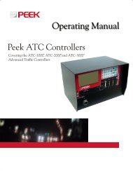
U.S. Traffic 170E-ATC - Peek Traffic
U.S. Traffic 170E-ATC - Peek Traffic
U.S. Traffic 170E-ATC - Peek Traffic
- No tags were found...

Create successful ePaper yourself
Turn your PDF publications into a flip-book with our unique Google optimized e-Paper software.
Chapter 5 — Theory of OperationSTATThis output from U13 pin 22 is an active low whenever the MPU requests a read of theCPU STATus port at address $5FFF.RTCRESRTCRES stands for ‘real-time clock reset’. This output from U13 pin 23 goes lowwhenever the MPU resets the Real Time Clock by writing to address $5FFF.MBENMBEN stands for ‘memory bus enable’. This output from U13 pin 25 goes low wheneverthe MPU accesses any address for any device located on the Memory Bus. It is used tocontrol bus buffer chips U27, U28 and U29.IOBENIOBEN stands for ‘input/output bus enable’. This output from U13 pin 26 goes lowwhenever the MPU accesses any device on the I/O Bus. It is used to control buffer chipU30.DTASDTAS stands for ‘down time accumulator seconds’. This output from U13 pin 24 goeslow whenever the MPU requests a read of the Downtime Accumulator Seconds registerat address $500F.VMA.EThis is a logic low whenever both the system Enable (E) and Valid Memory Address arehigh. It is used on the memory bus and is available from U16 pin 11. This chip is also abuffer and so this signal is used to feed directly onto the memory control bus.Bus Interface ComponentsThe CPU Card has two separate off-card bus interface structures: one for the I/O andone for memory. Chips U27 and U28 buffer the 16 address bits for the memory buscontrolled by the MBEN signal. These chips are therefore active only when the MPU isaccessing devices on this bus. The memory data bus is buffered by U29, againcontrolled by MBEN so that it is only active for accessing devices on this bus. Datadirection is controlled by the system R/W line. When this is high, U29 passes data fromthe backplane to the card local data bus. VMA.E (described above) is available from U16pin 11 while Memory ReaD (MRD) is buffered in U16 and available at pin 8.The I/O Bus has its addresses (bits AO to A3) and two control lines IOEN (Input OutputENable) and IORD (Input Output ReaD) buffered by U35. The I/0 data bus is bufferedby U30 which is controlled by IOBEN and the system R/W line. The system clockEnable signal (E) is buffered by U16 and is available on the I/O backplane as E fromU16 pin 6.Communications ComponentsThese comprise the 4 Asynchronous Communications Interface Adaptor (ACIA) chipsU4 to U7; 3 RS-232C interface chips U8 to U10; and the baud rate clock generatingcircuitry made up of U11 and U24 with the clock rate selector jumpers CLKSEL1 toCLKSEL4. The CPU oscillator frequency of 3.072 MHz from U11 pin 13 is taken to a34 U.S. <strong>Traffic</strong> <strong>170E</strong>-<strong>ATC</strong> Controller Operating Manual