

OmniVision's VGA wafer-level camera - I-Micronews
OmniVision's VGA wafer-level camera - I-Micronews
OmniVision's VGA wafer-level camera - I-Micronews

You also want an ePaper? Increase the reach of your titles
YUMPU automatically turns print PDFs into web optimized ePapers that Google loves.
F E B R U A R Y 2 0 1 2 I S S U E N ° 2 2<br />
W H A T ’ S I N S I D E ?<br />
OmniVision’s <strong>VGA</strong> <strong>wafer</strong>-<strong>level</strong><br />
<strong>camera</strong><br />
Whether it’s for the main <strong>camera</strong> of low-cost phones or the front-facing <strong>camera</strong><br />
of high-end phones, low-cost, low-resolution <strong>camera</strong> modules are extremely<br />
important.<br />
Wafer-<strong>level</strong> <strong>camera</strong>s<br />
In order to manufacture low-cost <strong>camera</strong> modules,<br />
the main cost drivers -- the image sensor, the<br />
optical module and the fi xture used to assemble the<br />
module to the phone board -- have to be reduced to<br />
a strict minimum.<br />
The image sensors lend themselves rather well<br />
to low-cost manufacturing due to their <strong>wafer</strong><strong>level</strong><br />
manufacturing approach. With this approach<br />
it is possible to manufacture optical lenses at<br />
the <strong>wafer</strong>-<strong>level</strong>, thus creating a very low-cost<br />
<strong>wafer</strong>-<strong>level</strong> optical module (or <strong>wafer</strong>-<strong>level</strong> optics,<br />
WLOptics). Another benefi t of WLOptics is their<br />
refl ow-compatible materials. By eliminating the<br />
plastic lenses used in standard optical modules, the<br />
<strong>camera</strong> modules become compatible with refl ow<br />
soldering, and thus can be integrated at the same<br />
time as the other surface mount components on the<br />
phone board.<br />
One way to optimize this refl ow compatibility is to<br />
package the image sensor at the <strong>wafer</strong>-<strong>level</strong> by<br />
redistributing the pads to the back side. This also<br />
reduces the <strong>camera</strong> module area to the image<br />
sensor area.<br />
OmniVision CameraCube<br />
A pioneer of the CMOS Image Sensor industry,<br />
OmniVision released its latest <strong>wafer</strong> <strong>level</strong> <strong>camera</strong>,<br />
the OVM7692, in 2010.<br />
OmniVision OVM7692 CameraCubeChip<br />
(Courtesy of System Plus Consulting)<br />
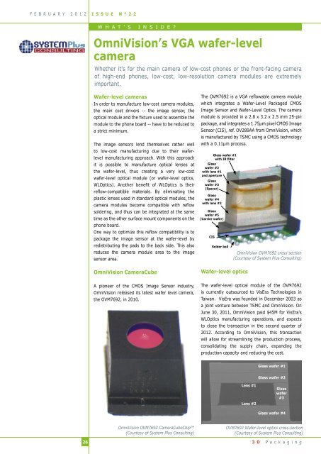
The OVM7692 is a <strong>VGA</strong> refl owable <strong>camera</strong> module<br />
which integrates a Wafer-Level Packaged CMOS<br />
Image Sensor and Wafer-Level Optics. The <strong>camera</strong><br />
module is provided in a 2.8 x 3.2 x 2.5 mm 25-pin<br />
package, and integrates a 1.75μm pixel CMOS Image<br />
Sensor (CIS), ref. OV289AA from OmniVision, which<br />
is manufactured by TSMC using a CMOS technology<br />
with a 0.11μm process.<br />
Glass <strong>wafer</strong> #1<br />
with IR fi lter<br />
Glass<br />
<strong>wafer</strong> #2<br />
with lens #1<br />
and aperture<br />
Glass<br />
<strong>wafer</strong> #3<br />
(Spacer)<br />
Glass<br />
<strong>wafer</strong> #4<br />
with lens #2<br />
Glass<br />
<strong>wafer</strong> #5<br />
(Carrier <strong>wafer</strong>)<br />
Solder ball<br />
Wafer-<strong>level</strong> optics<br />
OmniVision OVM7692 cross-section<br />
(Courtesy of System Plus Consulting)<br />
The <strong>wafer</strong>-<strong>level</strong> optical module of the OVM7692<br />
is currently outsourced to VisEra Technologies in<br />
Taiwan. VisEra was founded in December 2003 as<br />
a joint venture between TSMC and OmniVision. On<br />
June 30, 2011, OmniVision paid $45M for VisEra’s<br />
WLOptics manufacturing operations, and expects<br />
to close the transaction in the second quarter of<br />
2012. According to OmniVision, this transaction<br />
will allow for streamlining the production process,<br />
consolidating the supply chain, expanding the<br />
production capacity and reducing the cost.<br />
Lens #1<br />
Lens #2<br />
Glass <strong>wafer</strong> #1<br />
Glass <strong>wafer</strong> #2<br />
Glass<br />
<strong>wafer</strong><br />
#3<br />
Glass <strong>wafer</strong> #4<br />
OVM7692 Wafer-<strong>level</strong> optics cross-section<br />
(Courtesy of System Plus Consulting)<br />
26 3 D P a c k a g i n g<br />
CIS
The WLOptics of the OmniVision CameraCube<br />
consists of an assembly of four glass <strong>wafer</strong>s.<br />
The fi rst glass <strong>wafer</strong>, on top of the module, holds<br />
an IR fi lter (consisting of layers of Niobium oxide<br />
sandwiched with layers of Silicon oxide). The<br />
second glass <strong>wafer</strong> holds the fi rst lens. Next up is<br />
a spacer glass <strong>wafer</strong>, etched by powder blasting,<br />
which separates the second glass <strong>wafer</strong> from the<br />
fourth glass <strong>wafer</strong> -- which holds the second lens.<br />
The lenses are made with a UV curable polymer<br />
and are manufactured with a replication process.<br />
A plastic tool (likely Polydimethylsiloxane --PDMS<br />
silicone) molded into a master is used to imprint the<br />
polymer lenses. Each master can be used to make<br />
a large number of PDMS tools, and each PDMS tool<br />
can be used to imprint a large number of lenses.<br />
Wafer-<strong>level</strong> packaging<br />
The CMOS Image Sensor (CIS) is Wafer-Level<br />
Packaged (WLP) by Xintec, using a ShellCase RT<br />
process.<br />
Xintec obtained a license for the ShellCase CSP<br />
technology from ShellCase Ltd. in 2000 (Tessera<br />
has since acquired ShellCase Ltd. and now licenses<br />
the ShellCase technology to Xintec). The ShellCase<br />
process consists of a redistribution of the CIS pads<br />
to the back side through the edge of the die, using<br />
a “T-contact”.<br />
The packaging process begins with the bonding<br />
of a glass carrier substrate to the CIS <strong>wafer</strong>.<br />
Strengthened by its carrier substrate, the CIS <strong>wafer</strong><br />
100%<br />
90%<br />
80%<br />
70%<br />
60%<br />
50%<br />
40%<br />
30%<br />
20%<br />
10%<br />
0%<br />
OVM7692 <strong>camera</strong> module cost<br />
breakdown<br />
Final test + Scrap<br />
(Omnivision)<br />
7%<br />
WL-Optic +<br />
Assembly (VisEra)<br />
25%<br />
CIS ShellCase<br />
WLP (Xintec)<br />
19%<br />
CIS Manufacturing<br />
(TSMC)<br />
49%<br />
3 D P a c k a g i n g<br />
Black<br />
coating<br />
T-contact<br />
Silicone<br />
epoxy<br />
can be thinned down to 130μm, and vias can be<br />
etched all around each CIS die. These vias are then<br />
fi lled with a conductive aluminum layer. Finally, a<br />
protective encapsulation is created and solder balls<br />
are produced.<br />
Cost structure<br />
Wafer-<strong>level</strong> manufacturing of all <strong>camera</strong> module<br />
elements results in a signifi cant reduction of the<br />
production cost – in fact, the OmniVision OVM7692’s<br />
total production cost is estimated to be under $1.<br />
Compared to standard <strong>camera</strong> modules where the<br />
cost is equally distributed between the three main<br />
cost drivers, the <strong>wafer</strong>-<strong>level</strong> <strong>camera</strong> module cost<br />
is especially impacted by the image sensor, which<br />
equates to about 50% of the total manufacturing<br />
cost.<br />
CMOS Image<br />
Sensor<br />
Glass Carrier <strong>wafer</strong><br />
Metal layer<br />
(Silver)<br />
Silicone epoxy Cavity<br />
Lead<br />
Glass<br />
<strong>wafer</strong> #1<br />
Glass<br />
<strong>wafer</strong> #2<br />
Glass<br />
<strong>wafer</strong><br />
#3<br />
Glass<br />
<strong>wafer</strong><br />
#4<br />
Glass<br />
Wafer #5<br />
(carrier <strong>wafer</strong>)<br />
I S S U E N ° 2 2 F E B R U A R Y 2 0 1 2<br />
CMOS Image Sensor<br />
Solder<br />
bump<br />
OVM7692 ShellCase CIS WLP cross-section<br />
(Courtesy of System Plus Consulting)<br />
Romain Fraux<br />
System Plus Consulting<br />
Camera Module<br />
Lens #1<br />
Lens #2<br />
AP layer<br />
Imaging Area<br />
with micro-lenses<br />
Romain Fraux,<br />
Electronics Cost<br />
Engineer,<br />
System Plus<br />
Consulting<br />
Romain Fraux is<br />
Project Manager<br />
for Reverse Costing<br />
analyses at System Plus Consulting.<br />
Since 2006, Romain is in charge of<br />
costing analyses of MEMS devices,<br />
Integrated Circuit and electronics<br />
boards. He has signifi cant experience<br />
in the modeling of the manufacturing<br />
costs of electronics components.<br />
Romain has a BEng from Heriot-Watt<br />
University of Edinburgh, Scotland and<br />
a master’s degree in Microelectronics<br />
from the University of Nantes, France.<br />
IR filter<br />
Black<br />
coating<br />
Cavity<br />
27<br />
T-Contact<br />
Wafer-<strong>level</strong><br />
Optics<br />
Wafer-<strong>level</strong><br />
Packaging<br />
OVM7692 structure & cost breakdown (Courtesy of System Plus Consulting)


