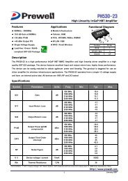
InGaP HBT Gain Block
InGaP HBT Gain Block
InGaP HBT Gain Block

Create successful ePaper yourself
Turn your PDF publications into a flip-book with our unique Google optimized e-Paper software.
PW110<strong>InGaP</strong> <strong>HBT</strong> <strong>Gain</strong> <strong>Block</strong>FeaturesApplicationsFunctional Diagram5 - 1000MHz26 dB <strong>Gain</strong> at 200MHz+19 dBm P1dB+34 dBm Output IP3Single Voltage SupplyLead-free / Green / RoHS-compliant SOT-89 PackageDescriptionBroadband <strong>Gain</strong> <strong>Block</strong>Mobile InfrastructureIF AmplifierCATV / DBSRFID / Fixed Wireless4Function123Pin No.RF IN 1RF OUT / Bias 3Ground 2,4The PW110 is a high performance <strong>InGaP</strong> <strong>HBT</strong> MMIC Amplifier and consists of Darlington pair amplifiers. Theamplifier features high linear performance, wideband operation, and high reliability. The PW110 operates from asingle voltage supply and requires only two DC-blocking capacitors, a bias resistor and an inductor for operation.The device is a general purpose buffer amplifier that offers high dynamic range in a low cost surface-mountableplastic SOT-89 packages.SpecificationsSymbol Parameters Units Freq. Min. Typ. Max.S21 <strong>Gain</strong> dB75 MHz26200 MHz26500 MHz25900 MHz23.5S11 Input Return Loss dBS22 Output Return Loss dB75 MHz200 MHz500 MHz900 MHz75 MHz200 MHz500 MHz900 MHz-13-15-16-16-14-18-14-12P1dBOutput Power @1dBcompressiondBm75 MHz200 MHz500 MHz900 MHz18.918.918.818 8900 MHz 18.8OIP3Output Third OrderinterceptdBm75 MHz200 MHz500 MHz900 MHz3433.53332NF Noise Figure dB75 MHz200 MHz500 MHz900 MHz1.71.71.81.9V / I Device voltage / current V/mA 4.74/68Rth Thermal Resistance °C/W 94Test Conditions : T=25°C, Supply Voltage=+8V, Rbias=47ohm, 50ohm System, OIP3 measured with two tones at an output power of +3dBm/tone separatedby 1MHz.http://www.prewell.com1December 2006
PW110<strong>InGaP</strong> <strong>HBT</strong> <strong>Gain</strong> <strong>Block</strong>Typical RF Performance for 200MHz Tuned Application CircuitSupply Bias Voltage = 8V, R(bias)=47 ohm, Current= 68mAFrequency MHz 75 200 500 700 900S21 dB 26.1 26.2 25.5 24.9 24.2S11 dB -13 -15 -16 -17 -18S22 dB -14 -18 -14 -12 -10P1dB dBm 18.9 18.9 18.8 18.4 17.9OIP3 @3dBm dBm 34.3 33.8 33.1 32.6 31.9Noise Figure dB 1.7 1.7 1.8 1.8 1.835<strong>Gain</strong> vs. Frequency0Input Return Loss0Output Return Loss30-5-5<strong>Gain</strong>(dB)25S11(dB)-10-15S22(dB)-10-1520 +25 o C-40 o C+85 o C150.0 0.2 0.4 0.6 0.8 1.0Frequency (GHz)+25 o C-20-40 o C+85 o C-250.0 0.2 0.4 0.6 0.8 1.0Frequency (GHz)+25 o C-20-40 o C+85 o C-250.0 0.2 0.4 0.6 0.8 1.0Frequency (GHz)40Output IP3 vs. Frequency25P1dB vs. Frequency3NF vs. FrequencyOIP3(dB Bm)35302520+25 o C+85 o C-40 o C0.2 0.4 0.6 0.8 1.0Frequency (GHz)P1dB(dB Bm)2015105+25 o C-40 o C+85 o C0.2 0.4 0.6 0.8 1.0Frequency (GHz))NF(dB)2100.0 0.2 0.4 0.6 0.8 1.0Frequency (GHz)+25 o COutput Power / <strong>Gain</strong> vs. Input Power @ 0.2GHz30Output Power / <strong>Gain</strong> vs. Input Power @ 0.9GHz30OutPut Power(dBm)/ P<strong>Gain</strong>(dB)252015105-20 -15 -10 -5 0 5Input Power(dBm)<strong>Gain</strong>Output PowerOutPut Power(dBm)/ <strong>Gain</strong>(dB)25201510<strong>Gain</strong>Output Power5-20 -15 -10 -5 0 5Input Power(dBm)2http://www.prewell.comDecember 2006
PW110<strong>InGaP</strong> <strong>HBT</strong> <strong>Gain</strong> <strong>Block</strong>200MHz Tuned Application CircuitRecommended e Bias ValuesSupplyVoltageSupply Voltage R bias Value SizeR Bias1uF7 V 32 Ω 12108 V 47 Ω 12109 V 62 Ω 2010RF IN820nH10nFRF OUT10 V 75 Ω 201012 V 107 Ω 251210nF10nFTypical RF Performance for 500 - 900MHz Tuned Application CircuitSupply Bias Voltage = 8V, R(bias)= 47 ohm, Current= 69mAFrequency MHz 500 700 900S21 : <strong>Gain</strong> dB 24.8 24.3 23.6S11 : Input Return Loss dB -15 -16 -16S22 : Output Return Loss dB -18 -15 -12Output P1dB dBm 19.4 19.5 18.8Output IP3 @3dBm dBm 32.8 32.6 32.0Noise Figure dB 1.9 1.9 1.9SupplyVoltage30<strong>Gain</strong> vs. FrequencyR Bias1uF25<strong>Gain</strong>(dB)20RF IN56nH56pFRF OUT15+25 o C56pF56pF10400 500 600 700 800 900 1000Frequency(MHz)0Input Return Loss0Output Return Loss-5-5S11(dB)-10-15S22(dB) S-10-15-20-25400 500 600 700 800 900 1000Frequency(MHz)+25 o C3-20-25400 500 600 700 800 900 1000Frequency(MHz)+25 o Chttp://www.prewell.comDecember 2006
Absolute Maximum RatingsPW110<strong>InGaP</strong> <strong>HBT</strong> <strong>Gain</strong> <strong>Block</strong>Parameter Rating UnitDevice Voltage +5 VDevice Current 150 mARF Power Input 10 dBmStorage Temperature -55 to +125 °CAmbient Operating Temperature -40 to +85 °CJunction Temperature 165 °COperation of this device above any of these parameters may cause permanent damage.Lead-free /RoHS Compliant / Green SOT-89 Package OutlineESD / MSL Ratings1. ESD sensitive device.Observe Handling Precautions.2. ESD Rating : Class 2(Passes at 2000V min.)Human Body Model (HBM), JESD22-A1143. ESD Rating : Class IV (Passes at 1000V min.)Charged Device Model (CDM), JESD22-C1014. MSL (Moisture Sensitive Level) Rating : Level 3at +260°C Convection reflow, J-STD-020Evaluation Board Layout (4x4)Mounting Instructions41. Use a large ground pad area with many platedthrough-holes as shown.2. We recommend 1 oz copper minimum.3. Measurement for our data sheet was made on0.8mm thick FR-4 Board.4. Add as much copper as possible to inner and outerlayers near the part to ensure optimal thermalperformance.5. RF trace width depends on the board material andconstruction.6. Add mounting screws near the part to fasten theboard to a heatsink.http://www.prewell.comDecember 2006