Phase Shifters and I-Q Modulators - Admiral Microwaves Ltd
Phase Shifters and I-Q Modulators - Admiral Microwaves Ltd
Phase Shifters and I-Q Modulators - Admiral Microwaves Ltd

You also want an ePaper? Increase the reach of your titles
YUMPU automatically turns print PDFs into web optimized ePapers that Google loves.
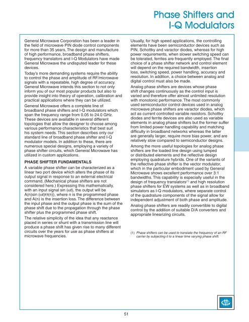
<strong>Phase</strong> <strong>Shifters</strong> <strong>and</strong>I-Q <strong>Modulators</strong>General Microwave Corporation has been a leader inthe field of microwave PIN diode control componentsfor more than 35 years. The design <strong>and</strong> manufactureof high performance, broadb<strong>and</strong> phase shifters,frequency translators <strong>and</strong> I-Q <strong>Modulators</strong> have madeGeneral Microwave the undisputed leader for thesedevices.Today’s more dem<strong>and</strong>ing systems require the abilityto control the phase <strong>and</strong> amplitude of RF/microwavesignals with a repeatable, high degree of accuracy.General Microwave intends this section to not onlyinform you of our most popular products but also toprovide insight into theory of operation, calibration <strong>and</strong>practical applications where they can be utilized.General Microwave offers a complete line ofbroadb<strong>and</strong> phase shifters <strong>and</strong> I-Q modulators whichspan the frequency range from 0.05 to 24.0 GHz.These devices are available in several differenttopologies that allow the designer to choose amongvarious performance characteristics that best suithis system needs. This section describes only ourst<strong>and</strong>ard line of broadb<strong>and</strong> phase shifter <strong>and</strong> I-Qmodulator models. In addition to these, there arenumerous special designs, employing a variety ofphase shifter circuits, which General Microwave hasutilized in custom applications.PHASE SHIFTER FUNDAMENTALSA variable phase shifter can be characterized as alinear two port device which alters the phase of itsoutput signal in response to an external electricalcomm<strong>and</strong>. (Mechanical phase shifters are notconsidered here.) Expressing this mathematically,with an input signal sin (ωt), the output will beA(n)sin (ωt)Θ(n)), where n is the programmed phase<strong>and</strong> A(n) is the insertion loss. The difference betweenthe input phase <strong>and</strong> the output phase is the sum of thephase shift due to the propagation through the phaseshifter plus the programmed phase shift.The relative simplicity of the idea that any reactanceplaced in series or shunt with a transmission line willproduce a phase shift has given rise to many differentcircuits over the years for use as phase shifters atmicrowave frequencies.Usually, for high speed applications, the controllingelements have been semiconductor devices such asPIN, Schottky <strong>and</strong> varactor diodes, whereas for highpower requirements, when slower switching speed canbe tolerated, ferrites are frequently employed. The finalchoice of a phase shifter network <strong>and</strong> control elementwill depend on the required b<strong>and</strong>width, insertionloss, switching speed, power h<strong>and</strong>ling, accuracy <strong>and</strong>resolution. In addition, a choice between analog <strong>and</strong>digital control must also be made.Analog phase shifters are devices whose phaseshift changes continuously as the control input isvaried <strong>and</strong> therefore offer almost unlimited resolutionwith monotonic performance. The most commonlyused semiconductor control devices used in analogmicrowave phase shifters are varactor diodes, whichact as current controlled variable resistors. Schottkydiodes <strong>and</strong> ferrite devices are also used as variableelements in analog phase shifters but the former sufferfrom limited power h<strong>and</strong>ling capability <strong>and</strong> matchingdifficulty in broadb<strong>and</strong> networks whereas the latterare generally larger, require more bias power, <strong>and</strong> arerelatively slow compared to semiconductor designs.Among the more useful topologies for analog phaseshifters are the loaded line design using lumpedor distributed elements <strong>and</strong> the reflective designemploying quadrature hybrids. One of the variants ofthe reflective phase shifter is the vector modulator,which in the particular embodiment used by GeneralMicrowave shows excellent performance over 3:1b<strong>and</strong>widths. This capability is especially useful in thedesign of frequency translators (1) <strong>and</strong> high resolutionphase shifters for EW systems as well as in broadb<strong>and</strong>simulators as I-Q modulators, where separate controlof the quadrature components of the signal allow forindependent adjustment of both phase <strong>and</strong> amplitude.Analog phase shifters are readily convertible to digitalcontrol by the addition of suitable D/A converters <strong>and</strong>appropriate linearizing circuits.(1) <strong>Phase</strong> shifters can be used to translate the frequency of an RFcarrier by subjecting it to a linear time varying phase shift.51
<strong>Phase</strong> <strong>Shifters</strong> <strong>and</strong>I-Q <strong>Modulators</strong>WHAT IS AN IQ VECTOR MODULATOR?An IQ Vector Modulator is an RF or microwave circuitwhich has the ability to control both the amplitude<strong>and</strong> phase of the transmitted signal simultaneously.Any sinusoidal signal can be expressed as a vectorhaving the properties of both amplitude <strong>and</strong> phasewith respect to a reference signal. If a signal isthought of as a vector in a polar coordinate systemwith coordinates of amplitude <strong>and</strong> phase, it can alsobe defined in a rectangular coordinate system withcoordinates of “I” <strong>and</strong> “Q”. The term “IQ” does notrepresent anything about the intelligence of the designengineer, but rather that the user can control both the“In-<strong>Phase</strong>” <strong>and</strong> “Quadrature-<strong>Phase</strong>” components of theoutput signal.WHAT IS A TYPICAL IQ MODULATOR CIRCUIT?The circuit typically includes an input power dividerwhich splits the incident signal into two paths, anamplitude <strong>and</strong>/or phase control element in each path,<strong>and</strong> an output signal summing circuit. In the simplestembodiment, the input signal is divided into two equalsignals with a 90° phase difference; controlled by aphase invariant bi-phase attenuator in each path; <strong>and</strong>combined by an in phase power combiner as shown infigure 1 on page 59.WHAT ACTIVE CONTROL COMPONENTS AREUSED IN IQ MODULATORS?The control components in an IQ vector modulatorare circuits that employ PIN diode, Schottky diodeor FET devices. The simplest circuit uses a PINdiode attenuator in series with a PIN-diode bi-phasemodulator, or a combination of the two devices ina single bi-phase attenuator. This device has theproperty of providing a continuous function which firstattenuates the input signal with no phase shift, thenshifts phase 180° at maximum attenuation, <strong>and</strong> thendecreases attenuation while holding a constant 180°phase shift. Balanced or double balanced Schottkydiode or FET mixers exhibit a similar function, but arelimited in dynamic range of attenuation. PIN diodedevices usually exhibit higher power h<strong>and</strong>ling, lowerinsertion loss <strong>and</strong> higher intercept points than Schottkydiode or FET based devices. Schottky diode or FETdevices are preferred for modulation rates higher thana few megahertz.WHAT ARE SOME OF THE USES OF IQ VECTORMODULATORS?• Amplitude <strong>and</strong> <strong>Phase</strong> control for RF simulatorsystems• Quadrature Amplitude Modulation• Cancellation of unwanted jamming signals• Cancellation of crosstalk between co-locatedcommunication systems• Cross-Polarization Cancellation• Doppler Simulation• Nulling of antenna reflections in monostatic radarsystems• Complex weights for <strong>Phase</strong>d Array Antennas• Linear Filter EqualizerHOW ARE IQ VECTOR MODULATORSCALIBRATED?Calibration of the IQ vector modulator for controlledamplitude <strong>and</strong> phase response is often performed bygenerating a “look-up” table using a vector networkanalyzer. To obtain the highest degree of accuracy, thecalibration should be performed in-situ. A discussion ofcalibration techniques is provided on page 58. WhenIQ vector modulators are used in a nulling systeman algorithm can readily be developed to adjust thevalues of I <strong>and</strong> Q in a closed loop fashion to achievethe desired system performance.CAN THE I-Q VECTOR MODULATOR BECUSTOMIZED FOR SPECIAL APPLICATIONS?General Microwave has customized many variationsof the IQ vector modulator for numerous applicationsranging from low cost designs to nuclear hardenedradar systems. Our sales <strong>and</strong> engineering staffare available to help you maximize your systemperformance by incorporating IQ vector modulators tomeet challenging system requirements52
Definitions <strong>and</strong>Typical PerformanceDEFINITION OF PARAMETERS<strong>Phase</strong> Shift:The difference in phase angle of the existing RF signalat a given frequency <strong>and</strong> phase shift setting referencedto the exiting signal at the same frequency with thephase shifter set to zero degree phase shift.Accuracy:The maximum deviation in phase shift from theprogrammed phase shift over the operating frequencyrange when measured at room temperature.Temperature Coefficient:The average rate of change in phase shift, asreferenced to the zero degree phase state, over the fulloperating temperature range of the unit. Expressed indegrees phase shift/degrees C.PM/AM:The maximum peak-to-peak change in insertion loss ofthe phase shifter at any phase state over the full 360°phase range.Switching Speed:The time interval from the 50% point of the TTL controlsignal to within 10° of final phase shift. This applies toa change in either direction between any two phasestates which differ by more than 22.5°.Carrier Suppression:When the phase shifter is operated as a frequencytranslator, the minimum ratio of carrier output power tothe translated carrier output power.Sideb<strong>and</strong> Suppression:When the phase shifter is operated as a frequencytranslator, the minimum ratio of any sideb<strong>and</strong> outputpower to the translated carrier output power.Translation Rate:When the phase shifter is used as a frequencytranslator, the translation rate is determined by dividingthe clock rate by the number of steps. Number of stepsis equal to 2" where n equals number of bits.TYPICAL PERFORMANCECHARACTERISTICSHARMONICS AND INTERMODULATIONPRODUCTSAll PIN diode control devices will generate harmonics<strong>and</strong> intermodulation products to some degree sincePIN diodes are non-linear devices. When compared todigital switched-bit designs, analog PIN diode phaseshifters are more prone to generate spurious signalssince the diodes function as current-variable resistors<strong>and</strong> are typically operated at resistance levels wheresignificant RF power is absorbed by the diode.The levels of harmonic <strong>and</strong> intermodulation productsgenerated by a phase shifter or I-Q modulator aregreatly dependent upon its design, the operatingfrequency, attenuation setting <strong>and</strong> input power level.Typical 2nd <strong>and</strong> 3rd order intercept performance for amoderately fast phase shifter, i.e. 500 nsec switchingspeed follows:Frequency2.0 GHz8.0 GhzTYPICAL INTERCEPT POINTS2nd OrderIntercept+35 dBm+40 dBm3rd OrderIntercept+30 dBm+35 dBmPHASE NOISEThe phase shifters <strong>and</strong> I-Q modulators offered byGeneral Microwave minimize the contribution of phasenoise to system performance. This is accomplishedby utilizing PIN diodes which are less sensitive to highfrequency noise than Schottky diodes, limiting thenoise b<strong>and</strong>width in driver control elements <strong>and</strong> the useof low noise buffer amplifiers to drive the PIN diodes.53
Theory of Operation &Practical ApplicationsI-Q VECTOR MODULATOR—THE IDEAL CONTROL COMPONENT!Microwave control components are used to vary signalamplitude <strong>and</strong> phase. Typically, they consist of twoportdevices including amplifiers, attenuators, phaseshifters, <strong>and</strong> switches. The I-Q vector modulator is aunique combination of active <strong>and</strong> passive devices thatis, in theory, ideally suited for the simultaneous controlof amplitude <strong>and</strong> phase.THEORY OF OPERATIONmagnitude of each of the signals, which are combinedin phase to yield the resultant vector. This vector willlie anywhere within the bounded area shown in Figure2. Thus, any signal applied to the l-Q vector modulatorcan be shifted in phase <strong>and</strong> adjusted in amplitude byassuming the desired attenuation level = x dB <strong>and</strong>the desired phase shift = Θ degrees. The normalizedoutput voltage magnitude is then given by:R = 10 –(x/20)The attenuation values of the I <strong>and</strong> Q attenuators arethen given by:I attenuator (dB) = 20 log (R cos Θ)Q attenuator (dB) = 20 log (R sin Θ)FIGURE 1I-Q Vector Modulator Block diagramThe block diagram of the I-Q vector modulator isshown in Figure 1. An RF signal incident on a 3 dBquadrature hybrid is divided into two equal outputs,with a 90 degree phase difference between them.The in-phase or 0 degree channel is designated the Ichannel <strong>and</strong> the quadrature or 90 degree channel isdesignated the Q channel. Each signal passes througha biphase modulator which selects the 0 or 180 degreestate for both the I <strong>and</strong> the Q paths. This defines thequadrant in which the resultant output signal resides(Figure 2). The attenuator in each path then varies theFIGURE 2I-Q <strong>Phase</strong> Relationship54
Theory of Operation &Practical ApplicationsTo achieve the desired phase shift, biphase modulatorstates must also be selected as shown in Table 1. Inthis way, the phase <strong>and</strong> amplitude of the output signalcan be varied simultaneously in a controlled fashion.TABLE 1Biphase Modulator StatesI QDesired <strong>Phase</strong> Shift0° 0° 0°-90°180° 0° 90°-180°180° 180° 180°-270°0° 180° 270°-360°AMPLITUDE BALANCEThe amplitude balance of the I <strong>and</strong> Q paths is asecond source of performance limitation. Unequalpower levels in these paths also produce errors in boththe amplitude <strong>and</strong> phase of the transmitted signal.To minimize this source of error, the quadraturehybridcoupling must be adjusted to provide minimumdeviation from the nominal 3 dB across the frequencyb<strong>and</strong>. For an ideal hybrid, the amplitude unbalancewill be ±0.31 dB over an octave b<strong>and</strong>. The effect ofamplitude <strong>and</strong> balance error on phase is shown inFigure 3.The theoretical model presupposes perfect amplitude<strong>and</strong> phase balance in the two signal paths, <strong>and</strong>ideal quadrature coupling in the 3 dB hybrid. To theextent that the conditions are not met in practice, theperformance of the I-Q vector modulator will be limited.PHASE BALANCEThe key element in determining the useful frequencyrange of the I-Q vector modulator is the 3 dBquadrature hybrid. Its most important characteristicis very low quadrature phase error (such as smalldeviation from 90 degree phase shift between outputs).To achieve this over a broad frequency range, weemploy the Hopfer quadrature hybrid (2) , which exhibitsextremely wideb<strong>and</strong> quadrature-phase properties(typically greater than 3 to 1 b<strong>and</strong>width with ±2-degreephase balance).In addition to using an in-phase Wilkinson combiner(which, with proper design, exhibits excellent phasebalance) the transmission-line length for the I <strong>and</strong> Qpaths must also be carefully phase-matched.FIGURE 3<strong>Phase</strong> Error Due to Amplitude ImbalanceNON-IDEAL BI-PHASE MODULATOR ANDATTENUATORErrors in amplitude <strong>and</strong> phase will occur if the biphasemodulator deviates from the ideal, eg: changes statefrom 0 to 180 degrees with constant amplitude orif the attenuator has an associated phase shift as(2) S. Hoofer, “A Hybrid Coupler for Microstrip Configuration,” IEEEMTT-S International Microwave Symposium Digest, 1979.55
Theory of Operation &Practical Applicationsattenuation is varied. Not only do these componentsin practice exhibit such deviations, but their interactingreflections may increase the resultant errorssignificantly. The arrangement in Figure 4 minimizesthe errors. As indicated, the t<strong>and</strong>em combination ofa biphase modulator <strong>and</strong> attenuator in each path isreplaced by a doubly-balanced biphase modulator.The doubly-balanced biphase modulator developedby General Microwave (3) has the ability to attenuatea signal by more than 20 dB with constant phase,then change the phase 180 degrees <strong>and</strong> return to thelow-loss state. At insertion loss, it exhibits a maximumphase error of less than ±6 degrees <strong>and</strong> an amplitudebalance of ±0.5 dB over a 3 to 1 b<strong>and</strong>width.FIGURE 4Series 71/71 Block DiagramPRACTICAL APPLICATIONSPHASE SHIFTERSIf the doubly-balanced biphase-modulator conditionsare adjusted so that the magnitude of the resultantvector remains fixed, the I-Q vector modulator canbehave as a constant-amplitude phase shifter. Therelationships between the desired phase shift <strong>and</strong> the I<strong>and</strong> Q attenuation levels are given by:ı I ı 2 + ı Q ı 2 = 1I = cos ΘQ = sin Θwhere I <strong>and</strong> Q are normalized voltages.The relationship between the I <strong>and</strong> Q drive circuitrycan be generated in either analog or digital fashion.The analog circuit employs a broadb<strong>and</strong> quadraturehybrid to generate the drive signals. In the digitaldrive circuit, PROMS are used to provide the requiredrelationships between I <strong>and</strong> Q. See the SelectionGuide on page 61 for the General Microwave phaseshifter model numbers.FREQUENCY TRANSLATORSA signal-processing technique using a linear timevaryingphase shifter is one method of frequencytranslation. One principal use is in velocity deceptionfor ECM systems by providing false Doppler radarreturns.In a true Doppler radar situation, the reflected signalis translated in frequency in an amount proportionalto the radial velocity of the target. As a rule, thereare no harmonics or spurious signals accompanyingthe reflection. However, if the target is using velocitydeceptiontechniques, spurious signals may bepresent in the radar return because of the non idealperformance of the frequency translator. The presenceof these spurious signals will reveal that the Dopplerradar is being jammed. Therefore, it is critical foroptimum ECM system performance that the frequencytranslator suppress the carrier, harmonics <strong>and</strong> allunwanted sideb<strong>and</strong>s to the greatest extent possible.For the linear phase shifter, the principal factorsthat contribute to imperfect carrier suppression <strong>and</strong>sideb<strong>and</strong> generation are:2π errorThis is the deviation from 360 degrees when maximumphase shift is programmed.PM/AM errorThe amplitude change (AM) is a function of the phasechange (PM).<strong>Phase</strong> nonlinearityIt is the deviation from linear phase shift vs. time.Quantization errorThis term is usually negligible for phase resolutiongreater than 6 bits. It arises in a digital phase shifter,which only approximates linear phase shift withdiscrete phase steps.Flyback timeThis arises from the finite time required by the phaseshifter to return from 360 to 0 degrees.(3) Z. Adler <strong>and</strong> B. Smilowitz, “Octave-B<strong>and</strong> High-PrecisionBalanced Modulator,” IEEE MTT-S International MicrowaveSymposium Digest, 1984.56
Theory of Operation &Practical ApplicationsIn the I-Q modulator, since the network operates asa constant-velocity rotating vector, the 0 <strong>and</strong> 360degree phase states are exactly the same, <strong>and</strong> the 2πerror <strong>and</strong> flyback error are eliminated. In addition, theGeneral Microwave Series 77 provides 10 bits of digitalphase control (sufficient to eliminate the quantizationerror), while phase linearity is optimized by the useof PROM correction in the drive circuitry. Finally, thePM/AM error is minimized by using matched doublybalancedbiphase modulators, thereby reducing thiserror essentially to the difference in amplitude of the3 dB quadrature hybrid output ports. This amplitudeimbalance varies with frequency <strong>and</strong> generates aunique spurious sideb<strong>and</strong> during frequency translation.An additional PROM correction using RF operatingfrequency information can be employed to reduce thisspurious sideb<strong>and</strong> for customer requirements.FIGURE 5–Typical Carrier <strong>and</strong> Sideb<strong>and</strong> SuppressionGeneral Microwave Model 7728AFrequency TranslatorCOMPLEX I-Q VECTOR MODULATORSSystem requirements often call for a t<strong>and</strong>emconnection of phase shifters <strong>and</strong> attenuators toprovide independent control of magnitude <strong>and</strong> phaseof an RF signal. If tight tolerances are required forthe amplitude <strong>and</strong> phase accuracy, a look-up tableis usually incorporated in the system software tocalibrate the phase shift <strong>and</strong> attenuation across thefrequency range. This is a tedious job that entails thegeneration of an extensive amount of error correctiondata, obtained by alternately varying the phase shifter<strong>and</strong> attenuator over the dynamic range for each narrowfrequency b<strong>and</strong> where optimization is required. Theinclusion of an I-Q vector modulator in the system inplace of a discrete phase shifter <strong>and</strong> attenuator offersseveral distinct advantages. A single RF componentreplaces two separate units, thus reducing cost<strong>and</strong> eliminating interacting VSWR. The relationshipbetween the I <strong>and</strong> Q inputs <strong>and</strong> the desired amplitude<strong>and</strong> phase permits a tremendous reduction in theamount of data required for a look-up table. This isbecause the I <strong>and</strong> Q inputs are independent variablesfor the I-Q vector modulator, whereas the t<strong>and</strong>emconnection of attenuator <strong>and</strong> phase shifter exhibitlarge AM to PM <strong>and</strong> PM to AM pushing, creatingdependency between the amplitude <strong>and</strong> phase inputs.Depending on the frequency range <strong>and</strong> accuracyspecifications, the RF circuitry of the I-Q vectormodulator can be optimized to eliminate the need for alook-up table entirely.The I-Q Vector Modulator is ideally suited for use inEW Simulators, Adaptive Equalizers or Automatic Test/Calibration Systems where extremely high accuracy<strong>and</strong> repeatability are essential.See the Selection Guide on page 61 for the GeneralMicrowave I-Q Vector Modulator model numbers.The specifications of the General Microwave Series77 Digitally Controlled <strong>and</strong> Series 78 VoltageControlled Frequency Translators include 25 dB carriersuppression <strong>and</strong> 20 dB sideb<strong>and</strong> suppression overa three-to-one frequency range. Typical performancedata for carrier <strong>and</strong> sideb<strong>and</strong> suppression, of the 6 to18 GHz Model 7728A, are shown in Figure 5. Carrier<strong>and</strong> sideb<strong>and</strong> suppression of greater than 34 dB for afrequency translator covering a 15-percent b<strong>and</strong>widthat X b<strong>and</strong> over the operating temperature range of–54°C to +100°C have been achieved in productionquantities.57
Amplitude <strong>and</strong><strong>Phase</strong> CalibrationGeneral Microwave I-Q Vector modulators canbe calibrated to provide precision control on bothamplitude <strong>and</strong> phase over their full rated dynamicrange. The calibration is performed using a vectornetwork analyzer <strong>and</strong> a customer generated testprogram to achieve the utmost in accuracy. The mostfrequently used algorithm to accomplish this calibrationis described herein. This algorithm involves defining aunity circle <strong>and</strong> then employing an iterative techniqueto locate precise calibration values.Many factors contribute to the overall accuracy thatis achievable using any calibration routine for theI-Q vector modulator. It is important that the userfully underst<strong>and</strong> the limitations of measurements incalibrating these units at microwave frequencies. Forexample, it is imperative that the desired calibrationaccuracy not exceed the accuracy <strong>and</strong> repeatabilityof the microwave test equipment. Another factorwhich must be included in the overall calibrationaccuracy is the effects of temperature on the I-Qmodulator <strong>and</strong> the test equipment. Given that theuser has a thorough underst<strong>and</strong>ing of vector networkanalyzer measurements, the following will be usefulfor generating a calibration program for a digitallycontrolled I-Q vector modulator. (Note that an analogcontrolled unit can be calibrated in the same fashionusing the relationship that 000 hex equals zero volts<strong>and</strong> FFF hex equals ten volts on the I <strong>and</strong> Q controls.)1.0 The calibration routine is performed at discretefrequencies in the b<strong>and</strong> of interest. The calibrationwill be valid over an interval of frequencies centeredat the calibration frequency <strong>and</strong> will be limited by theamplitude <strong>and</strong> phase errors that occur as frequencyis varied. The highest calibration accuracy will occurwith minimum frequency interval size. However thismay require an excessive amount of calibration time<strong>and</strong> data storage. It is recommended that a calibrationinterval of 100 to 200 MHz be used in the center ofthe frequency range of the vector modulator <strong>and</strong> 25to 50 MHz be used at the b<strong>and</strong> edges. The optimumcalibration interval for any user must be determinedempirically by insuring that the maximum phase <strong>and</strong>amplitude error over the frequency calibration intervalis within the desired limits.2.0 Once the calibration interval <strong>and</strong> the calibrationfrequency have been chosen, the next step is todefine the I <strong>and</strong> Q axes <strong>and</strong> the magnitude of the unitcircle. For this example, the I axis is defined to bethe horizontal axis on the I-Q plane with control word000 (hex) being equivalent to a vector of approximatemagnitude 1.0 at an angle of zero degrees. In thesame fashion the Q axis is defined to be the verticalaxis on the I-Q plane with control word 000 (hex)equivalent to a vector of approximately magnitude 1.0at an angle of 90 degrees. Note that for both I <strong>and</strong> Q,the magnitude zero vector is approximately 7FF (hex)<strong>and</strong> the magnitude –1.0 vector occurs as FFF (hex).Following this procedure the definition of the I-Q planeis arrived at per the table below:I CONTROL(hex)TABLE 2Q CONTROL(hex)APPROX.VECTOR000 7FF 1.0 ANG 0°FFF 7FF 1.0 ANG 180°7FF 000 1.0 ANG 90°7FF FFF 1.0 ANG 270°58
Amplitude <strong>and</strong><strong>Phase</strong> Calibration3.0 The magnitude of the unit circle is determined byfinding the maximum insertion loss at the calibrationfrequency in each of the four states in table 2 above.Since by nature the I-Q plane is a square <strong>and</strong> not acircle (see figure 6), the maximum insertion loss willoccur at one of these four states. Once the maximuminsertion loss is determined, the I or Q values of theother three states in table 2 are adjusted to meet thesame maximum insertion loss level. Note that onlyeither I or Q should be adjusted to increase insertionloss at any state, not both. The I or Q value that isinitially set to 7FF (which is approximately the centerof the IQ plane) is not varied during this part of thecalibration since the amplitude of the unit circle is notaffected by small changes in the control input.4.0 Having thus defined the unit circle, the next stepis to scale the I <strong>and</strong> Q axes to allow for computationof I <strong>and</strong> Q values given the desired amplitude <strong>and</strong>phase. If the I <strong>and</strong> Q axes were perfectly linear <strong>and</strong>each consisted of 4096 equal increments (for a 12 bitcontrol), it would be possible to achieve the desiredamplitude <strong>and</strong> phase shift using only the sine <strong>and</strong>cosine relationships given in figure 6. In order toapproach the ideal case, the I <strong>and</strong> Q values for eachof the four states given in table 2 must be scaledif they differ from 000 or FFF (note that the controlinput at 7FF is not varied in this step). The scalingentails taking the difference between 2048 digitalcounts (equal to one half of the 12 bit control) <strong>and</strong> thenumber of counts required to equalize the insertionloss of each of the four states required for the unitcircle derived from step 3.0. For example, assumethat the I value at zero degrees (I=000, Q=7FF), isthe maximum insertion loss of the four states <strong>and</strong>that in order to achieve the same level of insertionloss at 180° (nominal value I=FFF, Q=7FF), I must belowered by 127 counts such that the new value for180° on the unity circle is I=F80, Q=7FF. In this casethe I axis for 1
Amplitude <strong>and</strong><strong>Phase</strong> Calibration5.1 Convert the desired amplitude to a ratio such thatthe desired amplitude <strong>and</strong> phase can be expressedas a magnitude (R) <strong>and</strong> phase (Θ). This is the desiredphase <strong>and</strong> amplitude change with respect to thenormalized point obtained in step 5.0.5.2 Solve for the required values of I <strong>and</strong> Q <strong>and</strong>multiply by appropriate scaling factor as outlined instep 4.0. I = (R*cos Θ)*SCALE, Q = (R*sin Θ)*SCALE.This process is essentially changing from polarcoordinates (amplitude <strong>and</strong> phase) to rectangularcoordinates I <strong>and</strong> Q.5.3 Change I-Q modulator control word to the valueobtained above <strong>and</strong> measure the resultant amplitude<strong>and</strong> phase. Compare the difference between thedesired vector (at the calibration frequency) <strong>and</strong>the measured vector. This difference vector will beadjusted by successive iterations until its amplitude<strong>and</strong> phase error from the desired value is lessthan the desired calibration accuracy value. Fromexperience, accuracy values of 0.1 dB <strong>and</strong> 1 degreeare reasonable calibration limits for attenuation levelsbelow 20 dB. However higher accuracy is achievablewith careful measurements.5.4 If the measured vector is within the error limits,store the I-Q value in the calibration table that is beingset up. If the error is larger than the limit, calculate theI <strong>and</strong> Q change that is necessary to reach the desiredvector. This is performed by changing both the desiredvector <strong>and</strong> the error vector back into rectangular I-Qcoordinates <strong>and</strong> calculating the difference in I <strong>and</strong> Qcontrol word required to reach the desired vector. It isrecommended that the I-Q steps taken be limited toone half of the calculated value in order to minimizehunting time. Repeat this process until the desiredpoint is reached within the accuracy limits.6.0 Complete calibration is usually performed bygenerating sets of constant amplitude circles on theI-Q plane. Data points can readily be interpolatedover the plane <strong>and</strong> therefore only a limited number ofactual calibration points are required. Our experienceshows that calibration points taken every 22.5 degreesaround a constant amplitude circle with a linearinterpolation of I <strong>and</strong> Q values to find intermediatephase angles is sufficient to achieve high accuracy.Constant amplitude circles should be calibrated every0.5 dB for the first two dB above insertion loss <strong>and</strong> 1.0dB increments beyond that level. Interpolation betweenconstant amplitude circles is also useful in minimizingdata collection. For applications that require highspeed (
<strong>Phase</strong> <strong>Shifters</strong> <strong>and</strong> I-Q <strong>Modulators</strong>Selection GuidePHASE SHIFTERS/FREQUENCY TRANSLATORSBI-PHASE MODULATORSI.Q. VECTOR MODULATORSFREQUENCY RANGE (GHz)0.5 2.0 4.0 6.0 8.0 12.0 18.0MODEL PAGE COMMENTS0.5 2.0 7720A/7820<strong>Phase</strong> shifter / Frequency translator,digital / analog2.0 6.0 7722A/78224.0 12.0 7724A/782477<strong>Phase</strong> shifter / Frequency translator,digital / analog<strong>Phase</strong> shifter / Frequency translator,digital / analog6.0 18.0 7728A/7828<strong>Phase</strong> shifter / Frequency translator,digital / analog6.0 18.0 7928 81Miniature <strong>Phase</strong> shifter / Frequencytranslator, Hermetically sealed,digital6.0 18.0 F1938 62 I.Q. Vector modulator, digital/analog0.5 2.0 7120/7220I.Q. Vector modulator, digital/analog2.0 6.0 7122/7222 I.Q. Vector modulator, digital/analog4.0 12.0 7124/7224 I.Q. Vector modulator, digital/analog656.0 18.0 7128/7228 I.Q. Vector modulator, digital/analog2.0 6.0 7322/7422I.Q. Vector modulator, digital/analogHigh Dynamic Range6.0 18.0 7328/742870I.Q. Vector modulator, digital/analogHigh Dynamic Range16.0 24.0 7329/7429I.Q. Vector modulator, digital/analogHigh Dynamic Range6.0 18.0 7328H 75I.Q. Vector modulator, High speedHigh Dynamic Range61
Model F1938Bi-<strong>Phase</strong> ModulatorWith Integrated Driver• Frequency range: 6-18 GHz• Differential phase shift: 180° ±10°• High speed: 5 nsec (10-90% RF)• Low VSWR <strong>and</strong> insertion loss• Small size, light weightThe Model F1938 is a high-speed 0° or 180° phaseshifter that operates over the 6 to 18 GHz frequencyrange. It features a double-balanced design thatprovides excellent phase accuracy over its entirefrequency range.The RF design is shown below. The currents requiredto switch the unit between states are provided by theintegrated driver, which is controlled by an externallogic signal.62
Model F1938SpecificationsPERFORMANCE CHARACTERISTICSFrequency Range .............................6 to 18 GHzDifferential <strong>Phase</strong> Shift (1) ..................180° ±10°Switching Characteristics (2)ON Time .......................................20 nsec maxOFF Time .....................................20 nsec maxRise Time .....................................5 nsec maxFall Time .......................................5 nsec maxInsertion Loss (1) ................................ 6 to 16 GHz, 3 dB max>16 to 18 GHz, 3.5 dB maxVSWR (1) ..............................................2.0 maxChange of Insertion Losswith <strong>Phase</strong> Shift .........................1.0 dB maxCarrier Suppression .........................20 dB minModulation Rate ................................10 MHz maxPower H<strong>and</strong>ling CapabilityWithout PerformanceDegradation ..............................1W cw or peakSurvival Power ............................. 2W average, 25W peak (1µsec maxpulse width)Power Supply Requirements ........... +5V ±5%, 65mA–12 to –15V, 20 mAControl CharacteristicsControl Input Impedance ................. Schottky TTL, two-unit load. (A unitload is 2 mA sink current <strong>and</strong> 50 µAsource current.)Control Logic .................................... Alternate applications of logic “0” (–0.3to +0.8V) <strong>and</strong> logic “1” (+2.0 to +5.0V)switches phase by 180°.(1) With option 85, within Frequency B<strong>and</strong> of 16 to 18 GHz will be:a. Insertion Loss: 4 dB maxb. Differential <strong>Phase</strong> Shift: 180° ±15°c. VSWR: 2.2:1 max(2) As measured with a phase bridge.63
Model F1938SpecificationsENVIRONMENTAL RATINGSOperating TemperatureRange ....................... –65° to +110°CNon-Operating TemperatureRange ....................... –65° to +125°CHumidity ...................... MIL-STD-202F, Method 103B,Cond. B (96 hrs. at 95%)Shock ........................... MIL-STD-202F, Method 213B,Cond. B (75G, 6 msec)Vibration ...................... MIL-STD-202F, Method204D, Cond. B (.06" doubleamplitude or 15G, whicheveris less)Altitude ........................ MIL-STD-202F, Method 105C,Cond. B (50,000 ft.)Temp. Cycling ............. MIL-STD-202F, Method 107D,Cond. A, 5 cyclesAVAILABLE OPTIONSOption No. Description3 SMA female control connector7 Two SMA male RF connectors10 One SMA (J1) male <strong>and</strong> one SMAfemale (J2) RF connector33 EMI filter solder-type control terminal85 SMA RF connectors (see note (1) page63 for specification change with thisoption)Dimensional Tolerances, unless otherwise indicated: .XX ±.02; .XXX ±.00564
Series 71, 12 Bit Digital <strong>and</strong> Series 72 AnalogI-Q Vector <strong>Modulators</strong>Both Series comprise a family of four solid-state PINdiode I-Q Vector <strong>Modulators</strong> covering the frequencyrange from 0.5 to 18 GHz in four b<strong>and</strong>s: 0.5 to 2 GHz,2 to 6 GHz, 4 to 12 GHz <strong>and</strong> 6 to 18 GHz. See Fig. 1.All models provide a full 360° range of phase shift<strong>and</strong> a minimum of 20 dB attenuation range at anyfrequency.• Simultaneous control of amplitude <strong>and</strong>phase• 0.5 to 18 GHz in four b<strong>and</strong>s: 0.5 to 2 GHz;2 to 6 GHz; 4 to 12 GHz; 6 to 18 GHz• 12 Bit digitally programmable (Series 71)• Analog control (Series 72)• High speed• Guaranteed monotonicity65
Series 71, 12 Bit Digital <strong>and</strong> Series 72 AnalogI-Q Vector ModulationsTHEORY OF OPERATIONThe block diagram of the I-Q Vector Modulator isshown in Figure 1. An RF signal incident on a 3 dBquadrature hybrid is divided into two equal outputs,with a 90° phase difference between them. The inphase,or 0°, channel is designated the I channel <strong>and</strong>the Quadrature, or 90°, channel is designated theQ channel. Each signal passes through a biphasemodulator which sets the 0° or 180° state <strong>and</strong> theattenuation level for both the I <strong>and</strong> Q paths. Theoutputs of the I <strong>and</strong> Q path are combined to yield theresultant vector which may fall anywhere within thebounded area shown in Figure 2. Any signal appliedto the I-Q Vector Modulator can be shifted in phase<strong>and</strong> adjusted in amplitude by applying the followingrelationships:1. Let the desired attenuation level = X dB <strong>and</strong> thedesired phase shift = θ° (with respect to 0 dB <strong>and</strong> 0°reference states).2. The normalized output voltage magnitude is givenby: ı V ı = 10 -(x/20) .3. The values of the I <strong>and</strong> Q attenuator control inputsare then expressed as:I = V cos θ<strong>and</strong>Q = V sin θ.Figure 3 shows the nominal value of I <strong>and</strong> Q vs. eitherdigital word (Series 71) or analog voltage (Series72). Thus, to achieve an attenuation level of 3 dBwith a phase offset of 112.5° (with respect to 0 dB<strong>and</strong> 0° reference states) the values of I <strong>and</strong> Q can becalculated as follows:V = 10 –(3/20) = 0.707I = 0.707 cos (112.5°) –.027Q = 0.707 sin (112.5°) +0.65From Figure 3, the control inputs to yield the desiredamplitude <strong>and</strong> phase are approximately:Analog Units (72 Series) Digital Units (71 Series)I = 5.78 volts 100101000000Q = 2.84 volts 010010001011While these values for I <strong>and</strong> Q will yield an outputsignal whose amplitude <strong>and</strong> phase are close to thenominal values over the entire operating frequencyrange of the vector modulator, the use of an iterativemeasurement procedure will determine the I <strong>and</strong> Qinputs which exactly define the desired parameter atany selected frequency.66
Series 71/72SpecificationsPERFORMANCE CHARACTERISTICSMODEL 7120/7220 7122/7222 7124/7224 7128/7228FREQUENCY 0.5-2.0 GHz 2.0-6.0 GHz 4.0-12.0 GHz 6.0-18.0 GHzINSERTION LOSS 13 dB 11 dB 12 dB 12 dBVSWR (MAX) 1.6 :1 1.8 :1 1.8 :1 2.0 :1POWER HANDLINGWITHOUT PERFORMANCEDEGRADATIONSURVIVAL POWER (MAX)ABSOLUTE INSERTIONPHASE ACCURACY VS.FREQUENCY (MAX)FINE GRAIN PHASERIPPLE (50 MHz) (MAX)VARIATION OF PHASE VS.TEMPERATURE (MAX)+7 dBm +20 dBm +20 dBm +20 dBm1W±15º2º pk-pk±0.1 deg./ ºCATTENUATION RANGE (MIN)VARIATION OF AMPLITUDEVS.TEMPERATURE (MAX)RESPONSE TIME (MAX)POWER SUPPLYCONTR OL INPUT71 SERIES72 SERIESCONTROL INPUTIMPEDA NCE71 SERIES72 SERIESENVIRONMENTAL RATINGSOperating TemperatureRange .............................. –54°C to +100°CNon-OperatingTemperature Range ........ –65°C to +125°CHumidity ............................. MIL-STD-202F, Method103B, Cond. B (96 hrs. at95%)Shock .................................. MIL-STD-202F, Method213B, Cond. B (75G, 6msec)Vibration ............................. MIL-STD-202F, Method204D, Cond. B (.06"double amplitude or 15G,whichever is less)Altitude ............................... MIL-STD-202F, Method105C, Cond. B (50,000 ft.)Temp. Cycling .................... MIL-STD-202F, Method107D, Cond. A, 5 cycles20 dB0.02 dB/ ºC0.5 µsec–12 to –15V @ 70 mA+12 to +15V @ 70 mA12 bit TTL for both I <strong>and</strong> Q inputs0 to +10V DC for both I <strong>and</strong> Q inputs40 µA max10 K ohmsACCESSORY FURNISHEDMating power/control connector (Series 71 only)AVAILABLE OPTIONSOption No. Description7 Two SMA male RF connectors10 One SMA male (J2) <strong>and</strong> one SMAfemale (J1) RF connector67
Seeries 71/72SpecificationsMODEL A B C D E F G H J71207122712471284.95±.03(125,7)3.25±.03(82,6)3.00±.03(76,2)3.38±.03(85,9)3.25±.03(82,6)3.00±.03(76,2)1.02(25,9).85(21,6).96(24,4)4.75±.01(120,7)3.05±.01(77,5)2.80±.01(71,1)3.12±.01(79,2)3.00±.01(76,2)2.75±.01(69,9)1.68(42,7)1.63(41,4)1.50(38,1).75(19,1)2.48(62,9)1.99(50,5) 1.631.83 (41,4)(46,5)1.63(41,4)1.50(38,1).73(18,5).64(16,3).76(19,3)J3 PIN FUNCTIONPIN FUNCTION PIN FUNCTION1 I-5 20 I-42 I-6 21 I-73 I-8 22 I-34 I-9 23 I-25 I-10 24 I-1 (LSB)6 I-11 25 I-12 (MSB)7 N/C 26 N/C8 +12 to +15V 27 N/C9 GND 28 GND10 GND 29 N/C11 –12 to –15V 30 N/C12 Q-3 31 N/C13 Q-2 32 Q-414 Q-1 (LSB) 33 N/C15 Q-5 34 N/C16 Q-6 35 Q-12 (MSB)17 Q-7 36 Q-1118 Q-8 37 Q-1019 Q-9MODEL7120712271247128WEIGHT (APPROX)13 oz. (369 gm)10 oz. (284 gm)10 oz. (284 gm)9 oz. (255 gm)Dimensional Tolerances, unless otherwise indicated: .XX ±.02; .XXX ±.00568
Series 71/72SpecificationsMODEL A B C D E F G H J72207222722472284.95±.03(125,7)3.25±.03(82,6)3.00±.03(76,2)3.38±.03(85,9)3.25±.03(82,6)3.00±.03(76,2)1.02(25,9).85(21,6).96(24,4)4.75±.01(120,6)3.05±.01(77,5)2.80±.01(71,1)3.12±.01(79,2)3.00±.01(76,2)2.75±.01(69,9)1.68(42,7)1.63(41,4)1.50(38,1).75(19,1)1.75(44,5)1.99(50,5) .901.83 (22,9)(46,5)1.63(41,4).78(19,8).73(18,5).64(16,3).76(19,3)MODEL7220722272247228WEIGHT (APPROX)13 oz. (369 gm)10 oz. (284 gm)10 oz. (284 gm)9 oz. (255 gm)Dimensional Tolerances, unless otherwise indicated: .XX ±.02; .XXX ±.00569
Series 73 12 Bit Digital <strong>and</strong> Series 74 AnalogHigh Dynamic Range I-Q Vector <strong>Modulators</strong>The new Series 73/74 represents the latest additionto General Microwave's existing line of PIN DiodeI.Q. Vector <strong>Modulators</strong>. Their performance hasbeen enhanced to provide a higher dynamic rangeof attenuation for today's more dem<strong>and</strong>ing systemapplications.All models incorporate multiple bi-phase modulatorsections to provide in excess of 60 dB attenuationrange at any frequency. All models are also capableof a full 360° range of phase shift. The series covers afrequency range of 2 GHz to 24 GHz in three b<strong>and</strong>s:2 GHz to 6 GHz, 6 GHz to 18 GHz, <strong>and</strong> 16 GHz to24 GHz. A simplified block diagram is shown in Fig. 1.• Simultaneous control of amplitude <strong>and</strong>phase over a 60 dB dynamic range• 2 to 24 GHz in three b<strong>and</strong>s:2 to 6 GHz; 6 to 18 GHz; 16 to 24 GHz• 12 Bit digitally programmable(Series 73)• Analog control (Series 74)• High speed• Guaranteed monotonicity70
Series 73 12 Bit Digital <strong>and</strong> Series 74 AnalogHigh Dynamic Range I-Q Vector <strong>Modulators</strong>THEORY OF OPERATIONThe block diagram of the I-Q Vector Modulator isshown in Figure 1. An RF signal incident on a 3 dBquadrature hybrid is divided into two equal outputs,with a 90° phase difference between them. The inphase,or 0°, channel is designated the I channel <strong>and</strong>the Quadrature, or 90°, channel is designated theQ channel. Each signal passes through a biphasemodulator which sets the 0° or 180° state <strong>and</strong> theattenuation level for both the I <strong>and</strong> Q paths. Theoutputs of the I <strong>and</strong> Q path are combined to yield theresultant vector which may fall anywhere within thebounded area shown in Figure 2. Any signal appliedto the I-Q Vector Modulator can be shifted in phase<strong>and</strong> adjusted in amplitude by applying the followingrelationships:1. Let the desired attenuation level = X dB <strong>and</strong> thedesired phase shift = θ° (with respect to 0 dB <strong>and</strong>0° reference states).2. The normalized output voltage magnitude is givenby: ı V ı = 10 –(x/20) .3. The values of the I <strong>and</strong> Q attenuator control inputsare then expressed as:I = V cos θ<strong>and</strong>Q = V sin θ.Figure 3 shows the nominal value of I <strong>and</strong> Q vs. eitherdigital word (Series 73) or analog voltage (Series74). Thus, to achieve an attenuation level of 3 dBwith a phase offset of 112.5° (with respect to 0 dB<strong>and</strong> 0° reference states) the values of I <strong>and</strong> Q can becalculated as follows:V = 10 –(3/20) = 0.707I = 0.707 cos (112.5°) –.027Q = 0.707 sin (112.5°) +0.65From Figure 3, the control inputs to yield the desiredamplitude <strong>and</strong> phase are approximately:Analog Units (73 Series) Digital Units (74 Series)I = 7.81 volts 110010000000Q = 1.50 volts 001010000000While these values for I <strong>and</strong> Q will yield an outputsignal whose amplitude <strong>and</strong> phase are close to thenominal values over the entire operating frequencyrange of the vector modulator, the use of an iterativemeasurement procedure will determine the I <strong>and</strong> Qinputs which exactly define the desired parameter atany selected frequency.71
Series 73/74SpecificationsMODEL 7322/7422 7328/7428 7329/7429FREQUENCY 2.0-6.0 GHz 6.0-18.0 GHz 16.0-24.0 GHzINSERTION LOSS14 dB15 dB 6-16 GHz16.5 dB >16-18 GHzVSWR (MAX) 1.8 :1 2.0 :1POWER HANDLINGWITHOUT PERFORMANCEDEGRADATIONSURVIVAL POWER (MAX)ABSOLUTE INSERTIONPHASE ACCURACY VS.FREQUENCY (MAX)FINE GRAIN PHASERIPPLE (50 MHz) (MAX)VARIATION OF PHASE VS.TEMPERATURE (MAX)ATTENUATION RANGE (MIN)VARIATION OF AMPLITUDEVS.TEMPERATURE (MAX)RESPONSE TIME (MAX)POWER SUPPLYCONTR OL INPUT73 SERIES74 SERIESCONTROL INPUTIMPEDA NCE73 SERIES74 SERIESPERFORMANCE CHARACTERISTICS±15º+20 dBm1W2º pk-pk±0.2 deg./ ºC60 dB0.04 dB/ ºC1.0 µsec–12 to –15V @ 100 mA+12 to +15V @ 100 mA12 bit TTL for both I <strong>and</strong> Q inputs0 to +10V DC for both I <strong>and</strong> Q inputs40 µA max10 K ohms16 dB 16-22 GHz18 dB >22-24 GHz2.0 :1 16-22 GHz2.2 :1 >22-24 GHz±15° 16-22 GHz±20° >22-24 GHzENVIRONMENTAL RATINGSOperating TemperatureRange ....................... –54°C to +100°CNon-OperatingTemperature Range . –65°C to +125°CHumidity ...................... MIL-STD-202F, Method 103B,Cond. B (96 hrs. at 95%)Shock ........................... MIL-STD-202F, Method 213B,Cond. B (75G, 6 msec)Vibration ...................... MIL-STD-202F, Method204D, Cond. B (.06" doubleamplitude or 15G, whicheveris less)Altitude ........................ MIL-STD-202F, Method 105C,Cond. B (50,000 ft.)Temp. Cycling ............. MIL-STD-202F, Method 107D,Cond. A, 5 cyclesACCESSORY FURNISHEDMating power/control connector (Series 73 only)AVAILABLE OPTIONSOption No. Description7 Two SMA (Type K-Model 7X29) male RFconnectors10 One SMA (Type K-Model 7X29) male(J2) <strong>and</strong> one SMA (Type K-Model 7X29)female (J1) RF connector72
Series 73/74SpecificationsMODEL A B C D E F G H J K7322732873294.00±.03(101,6)3.12±.03(79,2)3.25±.03(82,6)3.00±.03(76,2)3.00±.03(76,2)3.00±.03(76,2).88(22,4).88(22,4).82(20,8)3.80±.01(96,5)2.92± .01(74,2)3.00±.01(76,2)2.75±.01(69,9)2.75±.01(69,9)2.75±.01(69,9)1.50(38,1)1.50(38,1)1.50(38,1)1.90(48,3)1.82(46,2)1.69(42,9)2.00(50,8)1.56(39,6)1.69(41,1).68(17,3).68(17,3).65(16,5).10(2,9).10(2,9).12(3,0)J3 PIN FUNCTIONPIN FUNCTION PIN FUNCTION1 I-5 20 I-42 I-6 21 I-73 I-8 22 I-34 I-9 23 I-25 I-10 24 I-1 (LSB)6 I-11 25 I-12 (MSB)7 N/C 26 N/C8 +12 to +15V 27 N/C9 GND 28 GND10 GND 29 N/C11 –12 to –15V 30 N/C12 Q-3 31 N/C13 Q-2 32 Q-414 Q-1 (LSB) 33 N/C15 Q-5 34 N/C16 Q-6 35 Q-12 (MSB)17 Q-7 36 Q-1118 Q-8 37 Q-1019 Q-9MODEL732273287329WEIGHT (APPROX)12 oz. (341 gm)11 oz. (312 gm)11 oz. (312 gm)Dimensional Tolerances, unless otherwise indicated: .XX ±.02; .XXX ±.00573
Series 73/74SpecificationsMODEL A B C D E F G H J K7422742874294.00±.03(101,6)3.12±.03(79,2)3.25±.03(82,6)3.00±.03(76,2)3.00±.03(76,2)3.00±.03(76,2).88(22,4).88(22,4).82(20,8)3.80±.01(96,5)2.92± .01(74,2)3.00±.01(76,2)2.75±.01(69,9)2.75±.01(69,9)2.75±.01(69,9)1.50(38,1)1.50(38,1)1.50(38,1)1.90(48,3)1.82(46,2)1.69(42,9)1.28(32,5).83(21,1).90(22,9).68(17,3).68(17,3).65(16,5).10(2,9).10(2,9).12(3,0)MODEL742274287429WEIGHT (APPROX)12 oz. (341 gm)11 oz. (312 gm)11 oz. (312 gm)Dimensional Tolerances, unless otherwise indicated: .XX ±.02; .XXX ±.00574
Model 7328H High Speed, High DynamicRange I-Q Vector ModulatorThe Model 7328H represents the latest advancementto General Microwave's comprehensive product line ofPIN diode I-Q Vector <strong>Modulators</strong>. Its response time hasbeen significantly reduced, resulting in an enhancedmodulation rate performance of 50 MHz to better servetoday's more dem<strong>and</strong>ing system applications.In addition to the high speed, the Model 7328Hincorporates multiple bi-phase modulator sectionsto provide in excess of 60 dB attenuation through 16GHz, <strong>and</strong> is capable of a full 360 degrees of phaseshift. Thus, the unit will provide high speed <strong>and</strong>simultaneous control of amplitude <strong>and</strong> phase over thefull frequency range of 6 to 18 GHz. A simplified blockdiagram is shown in Fig. 1.• High Speed – Modulation Rateof better than 50 MHz• Wide Frequency Range – 6 to18 GHz• Simultaneous control ofamplitude <strong>and</strong> phase over a60 dB dynamic range• Digitally Programmable I&Q– 12 Bit ECL control• Guaranteed monotonicityTHEORYThe Theory of Operation of the Model 7328H is thesame as the Series 73 units. The RF <strong>and</strong> Driverportions of the IQ Modulator have been modified toenable modulation rates up to 50 MHz.FIG. 1–SERIES 7328H BLOCK DIAGRAM75
Model 7328HSpecificationsPRELIMINARY PERFORMANCECHARACTERISTICSPARAMETERSPECIFICATIONFrequency Range, min .............. 6.0 to 18.0 GHzInsertion Loss, max ................... 16.0 dBVSWR, max ............................... 2.0 :1Power H<strong>and</strong>ling, maxWithout PerformanceDegradation ............................ –5 dBm TypicalSurvival ...................................... +27 dBmAbsolute Insertion <strong>Phase</strong> Accuracyvs Frequency ......................... ±15°Variation of <strong>Phase</strong>vs Temperature, max .............. ±0.2°/°CAttenuation range, min6 to 16 GHz ............................ 60dB>16 to 18 GHz ........................ 50dBVariation of Amplitudevs Temperature, max .............. 0.04 dB/°CModulation Rate, min ................. 50 MHzControl Input .............................. 12 Bit ECLfor both I&QControl Characteristics,I&Q, typ .................................. See Figure 2Control Input Impedance ........... 100 ohms(to –2V supply)Power Supply ............................. +12V @ 350 mA–12V @ 130 mA–5.2V @ 340 mA–2V @ 280 mADimensional Tolerances, unless otherwise indicated: .XX ±.02; .XXX ±.00576
Series 77, 10 Bit Digital <strong>and</strong> Series 78 Analog360° <strong>Phase</strong> <strong>Shifters</strong> & Frequency TranslatorsBoth Series, 77 <strong>and</strong> 78, comprise a family of eightsolid-state PIN diode phase shifters covering thefrequency range from 0.5 to 18 GHz in four b<strong>and</strong>s:0.5 to 2 GHz, 2 to 6 GHz, 4 to 12 GHz <strong>and</strong> 6 to 18GHz. All models provide a full 360° range of phaseshift <strong>and</strong> may also be used for frequency translationapplications.Each unit is an integrated assembly of an RF vectormodulator <strong>and</strong> a driver circuit, consisting of a 10-bitD/A converter <strong>and</strong> a voltage buffer in the Series 77digital units (see Fig. 1A) <strong>and</strong> a voltage converter<strong>and</strong> buffer in the Series 78 analog configuration(see Fig. 1 B).The voltage converter in the Series 78 consists ofan A/D converter followed by a 10-bit D/A converter,<strong>and</strong> converts a continuous analog input voltage intodiscrete steps of 0.35°.• 0.5 to 18 GHz in four b<strong>and</strong>s: 0.5 to 2 GHz;2 to 6 GHz; 4 to 12 GHz; 6 to 18 GHz• 10 Bit digitally programmable (Series 77)• Analog control (Series 78)• High speed• Guaranteed monotonicity77
Series 77/78Specifications<strong>Phase</strong> Shift<strong>Phase</strong> shift is achieved utilizing the RF vectormodulator approach shown in Fig. 2. The 3 dB hybridcoupler divides the RF signal into two quadraturecomponents which are then modulated in proportionto the sine <strong>and</strong> cosine of the desired phase shift.The signals are then combined in-phase to yield thephase-shifted output.Excellent phase accuracy <strong>and</strong> PM/AM performance(see Figs. 4 <strong>and</strong> 5) are achieved by using linearizeddouble balanced modulators. In their main operatingb<strong>and</strong>s, phase accuracy is better than ±10° up to10 GHz <strong>and</strong> ±12° to 18 GHz. This phase accuracycan be extended to cover the b<strong>and</strong> edges by using abuilt-in frequency correction circuit. Switching speed isbetter than 500 nsec.Frequency Translation (Serrodyning)Special attention in the design of the units hasbeen paid to those characteristics which affect theirperformance as frequency translators. These includeminimizing PM-to-AM conversion, use of high slewrate drivers, <strong>and</strong> optimizing phase shift linearity withapplied signal. As a result, carrier <strong>and</strong> sideb<strong>and</strong>suppression levels of over 25 <strong>and</strong> 20 dB, respectively,are obtained in the main b<strong>and</strong>s. The same carrier <strong>and</strong>sideb<strong>and</strong> performance can be realized over the fullstretch b<strong>and</strong> when the internal frequency correctioncircuit is employed.See Fig. 3 for input voltage control requirements forSeries 77 <strong>and</strong> 78 when used as a frequency translator.On special order, frequency translators can beprovided for operation over reduced b<strong>and</strong>widths withsuppression levels of up to 35 dB. Consult the factoryfor special requirements.PERFORMANCE CHARACTERISTICSSERIES 77Control ..........................10 bit TTLLogic InputLogic “0” (Bit OFF) ... –0.3 to +0.8V @ 500 µA maxLogic “1” (Bit ON) ..... +2.0 to +5.0V @ 100 µA maxPower Supply ............... +5V at 200 mA+12 to +15V @ 100 mA max–12 to –15V @ 90 mA maxSERIES 78Control Voltage ............0 to +6VSensitivity .....................23.4 mV/LSBResolution ....................1.41°Step Uncertainty ..........0.7° max, 0.3° typ.Input Resistance ..........2K ohmsPower Supply ............... +5V at 300mA+12 to +15V at 125 mA–12 to –15V at 50 mACOMMON TO BOTH SERIES 77 & 78Power H<strong>and</strong>ling CapabilityWithout PerformanceDegradation .............. +20 dBm (+7 dBm for 7720A,7820)Survival .........................+30 dBmHarmonics ....................–30 dBc<strong>Phase</strong> Variation ............0.1°/°C78
MODELNOS.7720A & 78207722A & 78227724A & 78247728A & 7828PHASE SHIFTER SPECIFICATIONSFREQUENCY RANGE (GHz)Main B<strong>and</strong> 0.7-1.85Stretch B<strong>and</strong> 0.5-2.0Main B<strong>and</strong> 2.6-5.2Stretch B<strong>and</strong> 2.0-6.0Main B<strong>and</strong> 4.5-10.5Stretch B<strong>and</strong> 4.0-12.0Main B<strong>and</strong> 8.0-18.0Stretch B<strong>and</strong> 6.0-18.0INSERTIONLOSS (Max.)11.5 dB13.0 dB10.0 dB11.0 dB10.5 dB12.0 dBOTHER SPECIFICATIONSSwitching Speed (50% TTL to within 10° of Final <strong>Phase</strong> Value); 500 nsec Max.Minimum phase shift range:Series 77: 360° in 1024 Steps (1o-bit) Series 78: 360° @ 60°/VoltTRANSLATIONRATE (Min.)VSWR(Max.)1.751.61.812.0 dB 2.0FREQUENCY TRANSLATOR SPECIFICATIONSCARRIER (1)SUPPRESSION (Min.)0 to 500 kHz (2) Main B<strong>and</strong>: 25 dBStretch B<strong>and</strong>: 18 dBSIDEBAND (1)SUPPRESSION (Min.)Main B<strong>and</strong>: 20 dBStretch B<strong>and</strong>: 15 dBSeries 77/78SpecificationsACCURACY (1)(Max.)±10°±15°±10°±15°±10°±15°±12°±15°PM/AM(Max.)±1.1 dB±2.5 dB±1.1 dB±1.5 dB±1.1 dB±2.0 dB±1.1 dB±2.0 dBINSERTION LOSSVARIATION (Max.)with translation rate:200 kHz: 1 dB500 kHz: 3 dBNOTES:(1) When operating as a <strong>Phase</strong> Shifter outside the Main B<strong>and</strong> Frequency Range, a TTL Low (0) applied to the J3 Power/Control ConnectorFreq. Correction Pin (pin 3) will result in Stretch B<strong>and</strong> Frequencies exhibiting enhanced performance characteristics. The resultant InsertionLoss, Accuracy <strong>and</strong> PM/AM specifications will be the same as those shown for the Main B<strong>and</strong> Frequency Range. When using the unit as aFrequency Translator, similar enhanced performance can be achieved for Carrier & Sideb<strong>and</strong> Suppression.(2) All specifications are met using five or more most significant bits for 0 to 200 kHz translation rates. For 201-500 kHz translation rates, onlythe four most significant bits are used.TYPICAL PERFORMANCE79
Series 77/78SpecificationsENVIRONMENTAL RATINGSOperating TemperatureRange ............................ –54°C to +100°CNon-OperatingTemperature Range ...... –65°C to +125°CHumidity ........................... MIL-STD-202F, Method103B, Cond. B (96 hrs. at95%)Shock ................................ MIL-STD-202F, Method213B, Cond. B (75G,6 msec)Vibration ........................... MIL-STD-202F, Method204D, Cond. B (.06"double amplitude or 15G,whichever is less)Altitude ............................. MIL-STD-202F, Method105C, Cond. B (50,000 ft.)Temp. Cycling .................. MIL-STD-202F, Method107D, Cond. A, 5 cyclesACCESSORY FURNISHEDMating power/control connectorAVAILABLE OPTIONSOption No. Description7 Two SMA male RF connectors10 One SMA male (J2) <strong>and</strong> one SMAfemale (J1) RF connectorPinNo.123456789101112131415J3 PIN FUNCTIONSFunctionSeriesSeries77 (1) 78–12V to –15V –12V to –15V+12V to +15V +12V to +15VFreq. Correction Freq. CorrectionCircuit Select (3) Circuit Select“0” = B<strong>and</strong> Edge “0” = B<strong>and</strong> Edge1.4° (3) Not Used5.6° (3) Not Used45.0° (3) Not Used180.0° (MSB) (3) Not Used90.0° (3) Not UsedGround Ground (Sig)0.7° (3) Ground (PWR)22.5° Not Used2.8°Not Used11.3° Not Used.035° (LSB) Control Voltage+5V±0.5VDC (2) +5VNOTE:(1) Unused logic bits must be grounded.(2) Must not exceed +7VDC. See footnote (3) below.(3) Must not be greater than +0.3 VDC above voltage at pin 15.MODEL A B C D E F G H J K7720A 4.95 ± .03 3.38 ± .0378207722A78227724A7824(125,7)(85,9)3.25 ± .03 3.25 ± .03(82,6)(82,6)7728A 2.50 ± .03 3.00 ± .037828(63,5)(76,2)1.02(25,9)1.48(37,6).84(21,3)1.25(31,8).84(21,3)1.25(31,8).88(22,4)1.19(30,2)4.75 ± .01 3.12 ± .01(120,7)(79,2)3.05 ± .01 3.00 ± .01(77,5)(76,2)2.30 ± .01 2.75 ± .01(58,4)(69,9)2.62(66,5)1.63(41,4)1.50(38,1)1.69(42,9)1.992.48(62,9)(50,5) 1.631.83(46,5)1.63(41,4)(41,4)1.25(31,8).73(18,5)1.18(30,0).66(16,8)1.07(27,2).66(16,8)1.07(27,2).71(18,0)1.02(25,9).32(8,1).78(19,8).32(8,1).72(18,3).32(8,1).72(18,3).39(9,9).69(17,6)WEIGHT(APPROX)13 oz. (369 gm)15 oz. (425 gm)9 oz. (255 gm)10 oz. (284 gm)9 oz. (255 gm)10 oz. (284 gm)6 oz. (170 gm)8 oz. (227 gm)Dimensional Tolerances, unless otherwise indicated: .XX ±.02; .XXX ±.00580
Model 7928A Miniaturized 8 Bit360° <strong>Phase</strong> Shifter/Frequency Translator• 6 to 18 GHz• 360° range• High speed• Digitally programmable (8 Bits)• Guaranteed monotonicity• Hermetically Sealed• Miniaturized: less than 1.5 in 3The Model 7928A is a miniaturized, hermeticallysealed PIN diode phase shifter covering the frequencyrange from 6 to 18 GHz providing a full 360° rangeof variable phase shift. It can also be used to performfrequency translation.The unit is an integrated assembly of an RF vectormodulator <strong>and</strong> a driver circuit consisting of an 8-bit D/Aconverter <strong>and</strong> a voltage buffer. See Figure 1.PHASE SHIFT<strong>Phase</strong> shifting is achieved utilizing the RF vectormodulator approach shown in Figure 2. The 3-dBhybrid coupler divides the RF signal into twoquadrature components which are then biased inproportion to the sine <strong>and</strong> cosine of the desired phaseshift. The signals are then combined in-phase to yielddesired output.ACCURACYImproved phase accuracy <strong>and</strong> PM/AM performanceare achieved by using double-balanced bi-phase linearamplitude modulators. In the main operating b<strong>and</strong>,overall phase accuracy is better than 12°. The samephase accuracy can be achieved at the b<strong>and</strong> edges byusing a built-in frequency correction circuit.Switching speed is better than 500 nsec.FREQUENCY TRANSLATION(SERRODYNING)In the design of the Model 7928A special attentionhas been paid to those characteristics which affectits performance as a frequency translator. Theseinclude minimizing PM-to-AM conversion, use of highslew rate drivers, <strong>and</strong> optimizing phase shift linearitywith applied signal. As a result, carrier <strong>and</strong> sideb<strong>and</strong>suppression levels of over 25 <strong>and</strong> 20 dB, respectively,are obtained in the main b<strong>and</strong>. The same carrier <strong>and</strong>sideb<strong>and</strong> performance can be realized over the fullstretch b<strong>and</strong> when the internal frequency correctioncircuit is employed. See Fig. 3 for input controlrequirements.On special order, frequency translators can beprovided for operation over reduced b<strong>and</strong>widths withsuppression levels of up to 40 dB. Consult the factoryfor such requirements.Fig. 1–Model 7928A, block diagramFig. 2–RF Vector Modulator81
Model 7928ASpecificationsPHASE SHIFTER SPECIFICATIONSFREQUENCY RANGE (GHz)INSERTIONLOSS (Max.)VSWR(Max.)ACCURACY (1)(Max.)PM/AM (1)(Max.)Main B<strong>and</strong> 8.0-18.0Stretch B<strong>and</strong> 6.0-18.012.0 dB 2.0 :1±12°±15°±1.1 dB± 2.0 dBFREQUENCY TRANSLATOR SPECIFICATIONSTRANSLATIONRATE(Min.)CARRIER (1)SUPPRESSION(Min.)Main B<strong>and</strong>:25 dB0 to 500 kHz (2) Stretch B<strong>and</strong>:18 dBSIDE BAND (1)SUPPRESSION(Min.)Main B<strong>and</strong>:20 dBStretch B<strong>and</strong>:15 dBINSERTION LOSSVARIATION (Max.)with translation rate:200 kHz:1 dB500 kHz:3 dB(1) When operating as a <strong>Phase</strong> Shifter outside the Main B<strong>and</strong> Frequency Range, a TTL Low (0) applied to the J3 Power/Control ConnectorFreq. Correction Pin (pin R) will result in Stretch B<strong>and</strong> Frequencies exhibiting enhanced performance characteristics. The resultantInsertion Loss, Accuracy <strong>and</strong> PM/AM specifications will be the same as those shown for the Main B<strong>and</strong> Frequency Range. When using theunit as a Frequency Translator, similar enhanced performance can be achieved for Carrier & Sideb<strong>and</strong> Suppression.(2) All specifications are met using only the five most significant bits for translation rates of 0 to 200 kHz. For translation rates of 201 to500 kHz, only 4 most significant bits are used.PERFORMANCE CHARACTERISTICS<strong>Phase</strong> ShiftRange ...................................... 360° in 256 stepsVariation .................................. 0.1°/°CControl Input .............................. 8 Bit TTLSwitching Speed(50% TTL to within 10° ofFinal <strong>Phase</strong> Value ........................ 500 nsec maxHarmonics .................................. –30 dBcPower H<strong>and</strong>ling CapabilityWithout PerformanceDegradation ............................ +10 dBm(typically +13 dBm)Survival power ....................... +30 dBmPower SupplyRequirements ......................... +5V ±5%, 80 mA+12 to +15V, 10 mA–12 to –15V, 95 mA1 1 1 1 1 1 1 1Negative Frequency Translation1 1 1 1 1 1 1 1Positive Frequency Translation1 0 1 0 1 0 1 0DIGITALINPUT0 1 0 1 0 1 0 11 0 1 0 1 0 1 0DIGITALINPUT0 1 0 1 0 1 0 10 0 0 0 0 0 0 00 0 0 0 0 0 0 0T TBF T TBFNOTES: TBF should be less than 1% of T to achieve Translation Rate =1specified carrier <strong>and</strong> sideb<strong>and</strong> suppressionT + TBFFig. 3–Model 7928A Control input requirements.82
Model 7928ASpecificationsACCESSORY FURNISHEDMating power/control connectorENVIRONMENTAL RATINGSOperating TemperatureRange ............................ –54°C to +95°CNon-OperatingTemperature Range ...... –65°C to +125°CAVAILABLE OPTIONSOption No. Description7 Two SMA male RF connectors10 One SMA male (J1), <strong>and</strong> one SMAfemale (J2) RF connector49 High Rel screening(see table 1, page 43)DIMENSIONS AND WEIGHTMODEL 7928A PIN FUNCTIONSPINABCDEFHJKLMNPRFUNCTIONSGround+ 5V–12 to –15V1.4° (LSB)2.8°5.6°22.5°11.3°90°180° (MSB)+12 to +15V45°GNDFreq. CorrectionCircuit Select“0” = B<strong>and</strong> EdgeModel 7928AWt. 4.0 oz (113g) approx.Dimensional Tolerances: unless otherwise indicated: .XX ±.02; .XXX ±.00583
SwitchesGeneral Microwave switches cover the frequencyrange from 100 MHz to 40 GHz <strong>and</strong> are available invarious topologies ranging from single-pole singlethrow(SPST) to single-pole eight-throw (SP8T) inboth reflective <strong>and</strong> non-reflective configurations, <strong>and</strong> anonreflective SP16T unit.SWITCH TOPOLOGYThere are two fundamental methods of connecting PINdiodes to a transmission line to provide a switchingfunction: in series with the transmission line so thatRF power is conducted when the PIN diode is forwardbiased <strong>and</strong> reflected when reverse biased; or in shuntwith the transmission line so that the RF power isconducted when the diode is reverse biased <strong>and</strong>reflected when forward biased. A simple reflectiveSPST switch can be designed utilizing one or morePIN diodes in either configuration as shown in Fig. 1.A multi-throw switch essentially consists of acombination of SPST switches connected to acommon junction <strong>and</strong> biased so that each switch portcan be enabled individually. The common junction ofthe switch must be designed to minimize the resistive<strong>and</strong> reactive loading presented by the OFF ports inorder to obtain low insertion loss <strong>and</strong> VSWR for theON port. There are two basic methods of realizinga multi-throw switch common junction for optimumperformance over a broad frequency range. The firstemploys series mounted PIN diodes connected to thecommon junction. A path is selected by forward biasingits series diode <strong>and</strong> simultaneously reverse biasing allthe other diodes. This provides the desired low-losspath for the ON port with a minimum of loading fromthe OFF ports. The second method utilizes shuntmounted PIN diodes located a quarter wavelengthfrom the junction. The diode(s) of the selected ONport is reverse biased while the OFF ports are forwardbiased to create a short circuit across the transmissionline. As a result of the quarter wavelength spacing,the short circuits are transformed to open circuits atthe junction. By proper choice of transmission lineimpedances <strong>and</strong> minimization of stray reactanceit is possible to construct a switch of this type withlow insertion loss <strong>and</strong> VSWR over a three to oneb<strong>and</strong>width. The schematic diagrams for both switchesare shown in Fig. 2.84
SwitchesABSORPTIVE SWITCHESIt is often desirable to have a PIN diode switch presenta low VSWR in its OFF position as well as in its ONstate in order to maintain desired system performance.General Microwave offers a complete line of single<strong>and</strong> multi-throw absorptive switches which incorporate50Ω terminations in each of the output ports. Fig. 3shows the schematic diagrams of the two versions ofabsorptive (also known as nonreflective or terminated)switches employed by GMC. The shunt terminationis used in GMC's "all-series" configured absorptiveswitches which have a suffix ending in “T” or “W”. Thisstyle of absorptive switch offers the minimum penaltyin insertion loss due to the addition of the terminatingelements. The series termination is used in GMC'shigh speed “series-shunt” configured absorptiveswitches since it provides the optimum in switchingperformance.The common port of the st<strong>and</strong>ard absorptive multithrowswitches in the GMC catalog will be reflectivein the special circumstance when all ports are turnedOFF. If there is a need for this port to remain matchedunder these conditions, this can be realized eitherby employing an additional port to which an externaltermination is connected or, in a custom design,by providing automatic connection of an internaltermination to the common port.DEFINITION OF PARAMETERSINSERTION LOSS is the maximum loss measured ina 50 ohm system when only a single port of the switchis in the ON state.ISOLATION is the ratio of the power level when theswitch port is ON to the power level measured whenthe switch port is OFF. In a multi-throw switch theisolation is measured with one of the other portsturned ON <strong>and</strong> terminated in 50 ohms.VSWR is defined for the input <strong>and</strong> output ports of theselected ON path. For those switches with a “T”, “W”or “HT” suffix, the VSWR is also defined for the OFFstate.VIDEO LEAKAGEVideo leakage refers to the spurious signals presentat the RF ports of the switch when it is switchedwithout an RF signal present. These signals arisefrom the waveforms generated by the switch driver<strong>and</strong>, in particular, from the leading edge voltage spikerequired for high speed switching of PIN diodes. Whenmeasured in a 50 ohm system, the magnitude ofthe video leakage can be as much as several volts.The frequency content is concentrated in the b<strong>and</strong>below 200 MHz although measurable levels for highspeed switches are observed as high as 6.0 GHz.The magnitude of the video leakage can be reducedsignificantly by the inclusion of high pass or “videofilters” (1) in the switch, but the high frequency energywhich falls within the passb<strong>and</strong> of the switch can beeliminated only by using a slower speed switch.HARMONIC AND INTERMODULATIONPRODUCTSAll PIN diode switches generate harmonics <strong>and</strong>inter-modulation products since the PIN diodes arefundamentally non-linear devices. The magnitude ofthese spurious signals is typically small in a switchsince the diodes are usually either in their saturatedforward biased state or in their reversed biased state.The physics of the PIN diode cause a cut-off frequencyphenomena such that the level of harmonics <strong>and</strong>intermods greatly increase at low frequencies. Theselevels will vary with the minority carrier lifetime of thediode. Thus, a high speed switch operating below500 MHz may have a second order intercept point of35 dBm, while a slow switch operating at 8 GHz willhave a second order intercept point of 70 dBm. Typicalperformance is as follows:TYPICAL SWITCH INTERCEPT POINTSSWITCHHIGH SPEEDLOW SPEEDFREQUENCY2.0 GHz2.0 GHz2nd OrderINTERCEPT+50 dBm+65 dBm3rd ORDERINTERCEPT+40 dBm+50 dBmSince these levels vary significantly with frequency,switching speed, <strong>and</strong> RF topology, please consult thefactory for specific needs in this area.(1) For switches with internal video filters, specify Option 41, Option 42, or Option 43. These filters reduce the leakage as shown in the chartfollowing the power h<strong>and</strong>ling discussion on page 87.85
SwitchesSWITCHING SPEED (2)Port-To-Port Switching is the interval from the timethe RF power level at the off-going port drops to 90%of its original value to the time the RF power level inthe on-going port rises to 90% of its final value. SeeFig. 4.Rise Time is measured between the 10% <strong>and</strong> 90%points of the square-law detected RF power when theunit is switched from full OFF to full ON. See Fig. 5.Fall Time is the time between the 90% <strong>and</strong> 10% pointsof the square-law detected RF power when the unit isswitched from full ON to full OFF.On Time is measured from the 50% level of the inputcontrol signal to the 90% point of the square-lawdetected RF power when the unit is switched from fullOFF to full ON.Off Time is measured from the 50% level of the inputcontrol signal to the 10% point of the square-lawdetected RF power when the unit is switched from fullON to full OFF.In addition to the above definitions, the followinginformation about switching performance may beuseful to the system designer.Switching To Isolation – Although catalog switchingspeed specifications are usually defined to the 10%level of detected RF (equivalent to 10 dB isolation), theuser of a switch may be more interested in the time theswitch requires to reach rated isolation. This latter timeis strongly dependent on the topology of the switch.For all-shunt mounted or combination series <strong>and</strong> shuntmounted topologies, the time to reach final isolation isusually less than twice the fall time. For an all-seriestopology, the time to reach final isolation may be asmuch as ten times the fall time.Switching To Insertion Loss – For multi-throwswitches, the ON time depends on whether theswitch is being operated in a commutating or singleport mode. In the former mode, switching speed isslower than in the latter due to the loading effect atthe junction of the port turning OFF. All switchingspeed measurements at GMC are performed in thecommutating mode.(2) For a unit without an integrated driver, the specifications apply toconditions when it is driven by an appropriately shaped switchingwaveform.86
SwitchesPHASE AND AMPLITUDE MATCHINGSwitches are available on a custom basis with phase<strong>and</strong>/or amplitude matching. Matching can be eitherbetween ports of a switch, between like ports ondifferent switches, or a combination of the two. Theuniformity of broadb<strong>and</strong> catalog switches is quite good<strong>and</strong> is usually better than ±0.75 dB <strong>and</strong> ±15 degreesover the entire operating frequency of the switch.Please consult the factory for special requirements.POWER HANDLINGThe power h<strong>and</strong>ling of PIN diode switches isdependent on the RF topology, forward <strong>and</strong> reversebiasing levels, <strong>and</strong> speed of the switch. This catalogaddresses both the maximum operating power levels<strong>and</strong> the survival limits of the components. Maximumoperating limits are usually set at the power levelwhich will cause the reversed biased diodes to beginconduction <strong>and</strong> thereby degrade the insertion loss,VSWR, or isolation of the switch. The survival powerlimits are based on the maximum ratings of thesemiconductors in the switch. For special applications,significantly higher operational power levels can beprovided, particularly for narrow b<strong>and</strong> requirements.Please consult the factory for specific applications.VIDEO FILTER OPTIONSApplicability: F91 <strong>and</strong> G91 Switch SeriesPeak to Peak (mV)B<strong>and</strong>width (MHz)Video Leakage with Video Filter Options: 50 max 100INSERTION LOSS DEGRADATIONOption Affected Ports Frequency Additional IL41 Common Port Only 1-12.4 GHz12.4-18 GHz0.1 dB0.2 dB42 Output Ports Only 1-12.4 GHz12.4-18 GHz0.1 dB0.2 dB43 All Ports 1-12.4 GHz12.4-18 GHz0.2 dB0.4 dBVSWR DEGRADATIONOption Affected Ports Frequency VSWR41, 42, 43 All Ports 1-4 GHz4-18 GHz* As shown for switches whose VSWR specification from 1-4 GHz is less than 1.7.No change for switches whose VSWR specification from 1-4 GHz is 1.7 or greater.1.7 :1*No ChangeOPTION 55 – EXTENDED FREQUENCIESAny switch in our catalog that covers 1-18 GHz can be modified to cover 0.5 to 18GHz with following specification changes:1. Specification for insertion loss <strong>and</strong> isolation from 0.5 to 1.0 GHz is the sameas the 1-2 GHz specification. VSWR degrades to 2.0 :1.2. Insertion loss in the 12.4-18 GHz b<strong>and</strong> increases by 0.3 dB, Consult factoryfor cost.87