estimation of path delays using vhdl logic simulation - LEDA
estimation of path delays using vhdl logic simulation - LEDA
estimation of path delays using vhdl logic simulation - LEDA

Create successful ePaper yourself
Turn your PDF publications into a flip-book with our unique Google optimized e-Paper software.
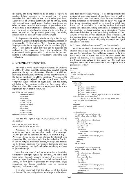
its output, but rising transition at an input is capable toproduce falling transition at the output only if risingtransition had previously arrived at the other gate input.Delay model <strong>of</strong> arbitrary complexity can be applied, takinginto account input signal slopes, loading capacitances andother parameters that influence ranges <strong>of</strong> gate <strong>delays</strong> tr andtf. Each time a delay attribute <strong>of</strong> output signal f is changed,an event must be scheduled to signal f with zero delay inorder to activate the processes performing the timing<strong>simulation</strong> in the gates driven by the NAND gate.To implement the timing <strong>simulation</strong> algorithm in <strong>logic</strong>simulator, a generalized signal attribute modeling mechanismis proposed in [2]. It is built in AleC++ hardware descriptionlanguage – the input language <strong>of</strong> Alecsis simulator [7]. InAleC++ user-defined signal attributes can be accessed andupdated in the processes during the <strong>simulation</strong>. Theexperimental results presented in [2] show that the proposedmethod is fast and appropriate for interactive use during <strong>logic</strong>verification.3. IMPLEMENTATION IN VHDLAlthough the user-defined signal attributes are availablein VHDL [87], they cannot be accessed and updated from theprocesses during the <strong>simulation</strong>. Therefore, a differentmodeling mechanism is necessary for the implementation <strong>of</strong>the timing <strong>simulation</strong> in VHDL simulator. We propose theuse <strong>of</strong> composite signals <strong>of</strong> the record type. Such acomposite signal consists <strong>of</strong> <strong>logic</strong> state and the timingattributes arr1mn, arr1mx, arr0mn, arr0mx, d1mn, d1mx,d0mn and d0mx. The record type DCSM_std_<strong>logic</strong> for the scalarsignals can be declared in VHDL as:type DCSM_std_<strong>logic</strong> is recordstatemn: std_u<strong>logic</strong>;d0mn: time;d1mn: time;arr0mn: boolean;arr1mn: boolean;statemx: std_u<strong>logic</strong>;d0mx: time;d1mx: time;arr0mx: boolean;arr1mx: boolean;end record DCSM_std_u<strong>logic</strong>;For the bus signals type DCSM_std_<strong>logic</strong>_vector can bedeclared as:type DCSM_std_<strong>logic</strong>_vector is array(natural range ) <strong>of</strong> DCSM_std_<strong>logic</strong>;Assuming the input and output signals <strong>of</strong> theDCSM_std_<strong>logic</strong> type, the complete model <strong>of</strong> a two-inputNAND gate can be described in VHDL as shown in Fig. 2.Processes labeled p1 and p2 are intended for standard <strong>logic</strong><strong>simulation</strong>. They model the <strong>logic</strong> function and delay function<strong>of</strong> the NAND gate. Processes labeled p3 and p4 are intendedfor the timing <strong>simulation</strong>. They monitor the timing attributes<strong>of</strong> gate inputs inp1 and inp2 and update the timing attributes<strong>of</strong> gate output oupt.Note that processes p3 and p4 are sensitive to the timingattributes <strong>of</strong> the input signals inp1 and inp2, but not to their<strong>logic</strong> states. Similarly, process p1 and p2 are sensitive toevents on input signal states, but not to their timing attributes.Hence, the two types <strong>of</strong> processes are independent. Logic<strong>simulation</strong> and timing <strong>simulation</strong> can be performedseparately or simultaneously.It is also important that the changes <strong>of</strong> the timingattributes <strong>of</strong> the output signal outp are always scheduled withzero delay in processes p3 and p4. If the timing <strong>simulation</strong> isinitiated at some time instant <strong>of</strong> <strong>simulation</strong> time, it will befinished at the same time instant, since the activity related totiming <strong>simulation</strong> is performed with no delay. We suggestthat timing <strong>simulation</strong> should be performed in initial timeinstant t=0 <strong>of</strong> <strong>simulation</strong>. If no timing attribute is changedduring the <strong>simulation</strong>, timing <strong>simulation</strong> is suppressed andthe simulator performs standard <strong>logic</strong> <strong>simulation</strong>. Timing<strong>simulation</strong> is invoked by setting the timing attributes arr1mn,arr1mx, arr0mn and arr0mx <strong>of</strong> primary inputs to value true. Ifthe primary inputs are grouped into a bus signal inp, thetiming analysis can be invoked by only one concurrent signalassignment command:inp ('0', 0 sec, 0 sec, true, true, '0', 0 sec, 0 sec, true, true));.Once the <strong>simulation</strong> time advances to t>0 sec, longest andshortest <strong>path</strong> <strong>delays</strong> <strong>of</strong> all signals in the circuit are availableand can be logged out. One additional process in the toplevelentity can be added that waits for some small timeperiod (for example, 1 pico second), prints the shortest andthe longest <strong>path</strong> <strong>delays</strong> to the screen or file, and thensuspends to the end <strong>of</strong> the <strong>simulation</strong>. An example <strong>of</strong> such aprocess is as follows:log: processbeginwait for 1 ps;--- print the timing analysis resultswait;end process log;entity nandg isgeneric (tpd_hlmn : time := 0.95 ns;tpd_lhmn : time := 1 ns;tpd_hlmx : time := 0.9 ns;tpd_lhmx : time := 1.05 ns);port (out1 : out DCSM_std_<strong>logic</strong> := ('0', 0.0 sec, 0.0 sec, false,false, '0', 0.0 sec, 0.0 sec, false, false);in1, in2: in DCSM_std_<strong>logic</strong> := ('0', 0.0 sec, 0.0 sec, false,false, '0', 0.0 sec, 0.0 sec, false, false));end nandg;architecture only <strong>of</strong> nandg isbegin---- Logic function:p1: process(in1.statemn, in2.statemn)variable val,ex_value : std_<strong>logic</strong> := '0';beginval := in1.statemn and in2.statemn;val := not (val);if val /= ex_value thenex_value := val;case val iswhen '0' =>out1.statemn out1.statemn end case;end if;end process p1;p2: process(in1.statemx, in2.statemx)variable val,ex_value : std_<strong>logic</strong> := '0';beginval := in1.statemx and in2.statemx;val := not (val);if val /= ex_value thenex_value := val;case val iswhen '0' =>out1.statemx out1.statemx end case;100