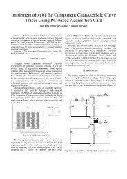
design for testability in an application specific dsp - LEDA
design for testability in an application specific dsp - LEDA
design for testability in an application specific dsp - LEDA

Create successful ePaper yourself
Turn your PDF publications into a flip-book with our unique Google optimized e-Paper software.
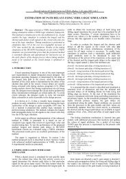
DESIGN FOR TESTABILITY IN AN APPLICATION SPECIFICDSPMilj<strong>an</strong>a Sokolović, Predrag PetkovićDepartment of Electronics, Faculty of Electronic Eng<strong>in</strong>eer<strong>in</strong>g, Beogradska 14, 18000 Nišmilj<strong>an</strong>a@ elfak.ni.ac.yu; predrag@ elfak.ni.ac.yuAbstract. Dur<strong>in</strong>g large DSP systems on chip <strong>design</strong>, one of the most import<strong>an</strong>t dem<strong>an</strong>d isassigned to fast <strong>an</strong>d efficient <strong>testability</strong> as well as the ability of defect diagnostics. This is veryimport<strong>an</strong>t consider<strong>in</strong>g expenses <strong>an</strong>d time consumption needed <strong>for</strong> circuit <strong>design</strong> <strong>an</strong>d potential<strong>design</strong> faults allocation. This paper presents <strong>an</strong> orig<strong>in</strong>al practical test<strong>in</strong>g problem solution <strong>in</strong> a<strong>specific</strong> <strong>application</strong> DSP cha<strong>in</strong> dedicated <strong>for</strong> <strong>in</strong>tegrated power-meter, that benefits BIST <strong>an</strong>d sc<strong>an</strong>test<strong>in</strong>g <strong>an</strong>d faults allocation techniques <strong>in</strong> a digital circuits. Practical <strong>application</strong> of the proposedsolution is confirmed by VHDL simulations.1. INTRODUCTIONThe aim of electronic circuit test<strong>in</strong>g is to determ<strong>in</strong>e whether the fabricatedcomponent, block or system operates well or not. But the velocity of <strong>design</strong> <strong>an</strong>dm<strong>an</strong>ufactur<strong>in</strong>g, <strong>in</strong>flicted by market, irrevocably leads to omissions that should besolved as fast as possible. If defects detect<strong>in</strong>g <strong>an</strong>d locat<strong>in</strong>g task would be faster <strong>an</strong>deasier, fabrication expenses would be signific<strong>an</strong>tly smaller <strong>an</strong>d the fabrication processfaster. Defect diagnostics is essential, especially <strong>in</strong> test chip fabrication. There<strong>for</strong>e, itis not just import<strong>an</strong>t to determ<strong>in</strong>e if the systems functionally fulfils all requirements,but also to discover where <strong>an</strong>d why the problem occurs. In early <strong>design</strong> <strong>an</strong>dfabricat<strong>in</strong>g phases, particularly <strong>in</strong> prototypes <strong>an</strong>d test chip <strong>design</strong>s, a special attentionis paid to diagnostics. As the <strong>design</strong> <strong>an</strong>d fabrication of test versions goes on, theaccent is mov<strong>in</strong>g from diagnostics to electronic circuits test<strong>in</strong>g.On the other h<strong>an</strong>d, signific<strong>an</strong>t numerosity, variety <strong>an</strong>d complexity of DSPsystems, require the use of some universal test<strong>in</strong>g technique that c<strong>an</strong> be applied to allDSP cha<strong>in</strong> build<strong>in</strong>g blocks, regardless to the function they per<strong>for</strong>m. Design ForTestability (DFT) <strong>an</strong>d Built In Self Test technique (BIST) pr<strong>in</strong>ciples are <strong>in</strong>flicted asgeneral solutions of this problem.This paper presents one DSP cha<strong>in</strong> test<strong>in</strong>g method. This DSP cha<strong>in</strong> is a part of<strong>in</strong>tegrated circuit used <strong>in</strong> power consumption measurement. The function of the DSPdiscussed is calculation of all relev<strong>an</strong>t variables referred to the energy meter<strong>in</strong>g,based on <strong>in</strong>st<strong>an</strong>t<strong>an</strong>eous values of voltage <strong>an</strong>d current <strong>in</strong> digital <strong>for</strong>m.The paper is org<strong>an</strong>ized as follows. The next section describes general pr<strong>in</strong>ciplesof DFT, BIST <strong>an</strong>d boundary sc<strong>an</strong> BS. Thereafter, a special attention will be paid to aparticular <strong>application</strong> <strong>specific</strong> DSP cha<strong>in</strong>. An orig<strong>in</strong>al test<strong>in</strong>g approach of such DSPsystem that benefits BIST <strong>an</strong>d sc<strong>an</strong> pr<strong>in</strong>ciples will be described next.A complete logic that the test<strong>in</strong>g method is based on, is described <strong>an</strong>d simulated<strong>in</strong> VHDL. In this way, a functionality of the solution described as well as itsuniversality of apply<strong>in</strong>g to <strong>an</strong>y other DSP cha<strong>in</strong> is confirmed. At the end simulationresults will be shown.
2. DFT, BIST AND BS TESTING PRINCIPLESIn general, DFT presents a circuit <strong>design</strong> that enables efficient circuit test<strong>in</strong>g withthe ability of detect<strong>in</strong>g as m<strong>an</strong>y faults as possible. The most often <strong>an</strong>d the simplestapproach is <strong>in</strong>corporat<strong>in</strong>g <strong>an</strong> additional test logic that c<strong>an</strong> <strong>in</strong>crease controllability <strong>an</strong>dopservability. However, this method is not suitable <strong>for</strong> very large <strong>in</strong>tegrated circuits,where regardless to the big number of p<strong>in</strong>s, some more, used just <strong>for</strong> test<strong>in</strong>g, have tobe added. Partial solution of this problem c<strong>an</strong> be the use of additional multiplexers, asshown <strong>in</strong> Figure 1. Us<strong>in</strong>g them, primary <strong>in</strong>puts (PI) <strong>an</strong>d primary outputs (PO) areadded <strong>an</strong> alternative tasks related just to test<strong>in</strong>g [1].PILog icL 1M1NLog icL 2M2POFigure 1. Increas<strong>in</strong>gcontrollability <strong>an</strong>dopservability without<strong>in</strong>crease the number ofexternal p<strong>in</strong>sOne control p<strong>in</strong> (M 1 ) c<strong>an</strong> select a various number of <strong>in</strong>ternal po<strong>in</strong>ts (of the logicL 2 ), to isolate them from their usual stimulus, <strong>an</strong>d to connect them directly to primary<strong>in</strong>puts. The second control signal (M 2 ) enables the connection between variousnumber of primary <strong>in</strong>puts <strong>an</strong>d <strong>in</strong>ternal po<strong>in</strong>ts (the outputs of the logic L 2 ). Thisconcept c<strong>an</strong> offer two operat<strong>in</strong>g modes:1. normal operat<strong>in</strong>g mode (M 1 M 2 =00);2. test<strong>in</strong>g L 1 – value at node N is tr<strong>an</strong>sferred to the primary output (M 1 M 2 =01)3. test<strong>in</strong>g L 2 – value at node N is controlled by the signal at the primary <strong>in</strong>put(M 1 M 2 =10)The efficiency of the proposed DFT method depends on the ability to isolate alltest<strong>in</strong>g blocks <strong>in</strong> the test<strong>in</strong>g phase. It is usual to per<strong>for</strong>m I/O operations us<strong>in</strong>g theserial port <strong>in</strong> order to m<strong>in</strong>imize the number of <strong>in</strong>put/output p<strong>in</strong>s dedicated <strong>for</strong> test<strong>in</strong>g.Built In Self Test (BIST) is based on<strong>in</strong>corporation of test functions <strong>in</strong>to a chip[1], [2]. This approach c<strong>an</strong> overdo one bigdrawback. That is the difference between<strong>in</strong>ternal <strong>an</strong>d external b<strong>an</strong>dwidth.Architecture of the chip that is based onthis technique is shown <strong>in</strong> Figure 2.External NF signal controls test<strong>in</strong>g, <strong>an</strong><strong>dsp</strong>ecial <strong>in</strong>ternal cells generate test signals<strong>an</strong>d collects the <strong>in</strong><strong>for</strong>mation about theirresponse.External"NF" testequipmentBISTmodulBISTmodulBISTmodulLog icMe m oryAnalogsub systemFigure 2. Architecture of the BIST chipThe IEEE st<strong>an</strong>dard 1149.1 def<strong>in</strong>es BS method. This st<strong>an</strong>dard assumes <strong>an</strong>additional built <strong>in</strong> test logic that simplifies the system logic test<strong>in</strong>g as well as theenvironment test<strong>in</strong>g [3], [4]. A chip realized accord<strong>in</strong>g to this st<strong>an</strong>dard consists of
system logic that per<strong>for</strong>ms its primary function, <strong>an</strong>d additional test logic as shown <strong>in</strong>figure 3.BSRSsystem logic<strong>in</strong>putsSystemlogicSsystem logicoutputsBRIRTDITMSTCKTestlogic(exept BSR)TDOTDITMSTCKTA PcontrolerOutputlo gicTDOFigure 3. The structure of <strong>an</strong> IEEE 1149.1st<strong>an</strong>dard based chipFigure 4. Block diagram of the test logicFigure 4 shows build<strong>in</strong>g blocks of the test logic: boundary-sc<strong>an</strong> register (BSR),bypass register (BR), <strong>in</strong>struction register (IR), TAP (test access port), controller <strong>an</strong>doutput logic. BSR is <strong>an</strong> array of BS cells (BSC) <strong>an</strong>d c<strong>an</strong> be serially written <strong>an</strong>d read.BSCs are memory elements placed on the boundary of <strong>an</strong> <strong>in</strong>tegrated circuit. A signalfrom the primary <strong>in</strong>put must go through one BSC <strong>in</strong> order to reach the system logic.Similarly, a signal from the output of the system logic must go through one BSC <strong>in</strong>order to reach a primary output.Watched from the outside, a chip based on this st<strong>an</strong>dard has four additional p<strong>in</strong>s.Namely these are TDI – Test Data In, TDO – Test Data Out, TMS – Test ModeSelect <strong>an</strong>d TCK – Test Clock. All of them <strong>for</strong>m a port <strong>for</strong> test<strong>in</strong>g called Test AccessPort (TAP).Exist<strong>in</strong>g so m<strong>an</strong>y different test<strong>in</strong>g pr<strong>in</strong>ciples implies that none of them is ideal.DFT method requires additional test<strong>in</strong>g p<strong>in</strong>s, which <strong>in</strong>creases the chip area. Us<strong>in</strong>gserial port relaxes this problem, but <strong>in</strong> turn, reduces test<strong>in</strong>g speed.The ma<strong>in</strong> disadv<strong>an</strong>tage of BIST technique occurs <strong>in</strong> large circuits, because they<strong>in</strong>evitably <strong>in</strong>crease the test<strong>in</strong>g block size. Similar observation st<strong>an</strong>ds <strong>for</strong> the BSmethod although a serial port c<strong>an</strong> also be assumed as a disadv<strong>an</strong>tage.All described techniques suffer of diagnostics disability. In the scope of chipprototyp<strong>in</strong>g this becomes a serious disadv<strong>an</strong>tage.3. DSP CHAIN IN AN INTEGRATED POWER-METERLet us consider one of DSP cha<strong>in</strong> solutions used with<strong>in</strong> electronic energymeter<strong>in</strong>g devices. It assumes a set of operations needed <strong>for</strong> active (P), reactive (Q)<strong>an</strong>d apparent power (S) calculations together with power factor (PF) <strong>an</strong>d current <strong>an</strong>dvoltage root me<strong>an</strong> square values (I rms <strong>an</strong>d V rms ) computation [5]. This cha<strong>in</strong> is shown<strong>in</strong> Figure 5.
Input signals are digitalvalues of <strong>in</strong>st<strong>an</strong>t<strong>an</strong>eousvoltage <strong>an</strong>d current. Thesedata are processed through aset of arithmetic operators, as<strong>in</strong>dicated <strong>in</strong> Figure 5.Actually, DSP consists ofseveral cha<strong>in</strong>s hav<strong>in</strong>g uniqueorig<strong>in</strong>.Calculation of I rms <strong>an</strong>dV rms is per<strong>for</strong>med accord<strong>in</strong>gto the def<strong>in</strong>ition of the rootme<strong>an</strong>s square value <strong>for</strong> thetime dependent signal x(t) <strong>in</strong>discrete <strong>for</strong>m:v(t)i(t)Voltage+HTCurrent+V ACoff+P off+Q offI ACoffSINC 2 N :NSINC 2 N :NFigure 5. DSP cha<strong>in</strong>N1 2X = ∑ X () i . (1)T i=1Second part of this cha<strong>in</strong> is used <strong>for</strong> calculation of P, Q, S <strong>an</strong>d PF. Additional circuitblocks here are Hilbert tr<strong>an</strong>s<strong>for</strong>mer (HT), as well as digital divid<strong>in</strong>g block. Activepower is determ<strong>in</strong>ed as a DC component of the product of <strong>in</strong>st<strong>an</strong>t<strong>an</strong>eous voltage <strong>an</strong>dcurrent, while the reactive power is determ<strong>in</strong>ed <strong>in</strong> the same m<strong>an</strong>ner, after the voltageis processed with<strong>in</strong> HT. Us<strong>in</strong>g these two results, the apparent power as well as thephase factor c<strong>an</strong> be calculated <strong>in</strong> the follow<strong>in</strong>g way:2 2S = P + Q , PF = P S(2)Considerable hardware sav<strong>in</strong>gs are ga<strong>in</strong>ed us<strong>in</strong>g the same functional blocks <strong>for</strong> moreoperations (<strong>for</strong> example, multiply<strong>in</strong>g <strong>an</strong>d add<strong>in</strong>g). All DSP cha<strong>in</strong> build<strong>in</strong>g blocks areconnected <strong>in</strong> series, without <strong>an</strong>y feedbacks <strong>an</strong>d loops. This fact simplifies test<strong>in</strong>g <strong>an</strong>ddiagnostics processes. The pr<strong>in</strong>ciple of built-<strong>in</strong> test logic will be described <strong>in</strong> detail<strong>in</strong> the follow<strong>in</strong>g section.4. TESTING AND DIAGNOSTICS PRINCIPLES IN AN APPLICATION SPECIFIC DSPA concept of described DSP cha<strong>in</strong> test<strong>in</strong>g is illustrated <strong>in</strong> Figure 6. It is based oneach operation block sc<strong>an</strong>n<strong>in</strong>g. A chip has four operat<strong>in</strong>g modes. Two modes of<strong>in</strong>terest are normal function <strong>an</strong>d test<strong>in</strong>g mode. Test<strong>in</strong>g mode offers two k<strong>in</strong>ds oftest<strong>in</strong>g. One is global test<strong>in</strong>g <strong>an</strong>d the other is detail test<strong>in</strong>g. Test<strong>in</strong>g logic consists ofcomparators, data registers (which are also used <strong>in</strong> a system logic) <strong>an</strong>d a signatureregister. The aim of the test is to determ<strong>in</strong>e whether the operator block functionswell. Each operator keeps oper<strong>an</strong>ds data <strong>in</strong> appropriate <strong>in</strong>put registers while the resultis stored <strong>in</strong> the output register. After process<strong>in</strong>g, the obta<strong>in</strong> output is compared withthe desired one. If the results match, the appropriate bit (correspond<strong>in</strong>g to theoperator under test) <strong>in</strong> signature register keeps flag “1”. However, registeredmalfunction sets the bit to “0”. Ones written “0” on a certa<strong>in</strong> bit position, c<strong>an</strong>not beoverwritten with <strong>an</strong>other value until the signature register is read.V effPPFSQI eff
A described concept presents a global test<strong>in</strong>g. It me<strong>an</strong>s that the process of globaltest<strong>in</strong>g consists of two phases. The first one is load<strong>in</strong>g the test vectors <strong>an</strong>d expectedresponse <strong>for</strong> every block. Then confirmation phase takes place. This concept fulfillsboth dem<strong>an</strong>ds, <strong>for</strong> fast test<strong>in</strong>g <strong>an</strong>d diagnostics.Besides, this test<strong>in</strong>g concept allowsi(t)v(t)serial I/O portv'(t)busregisterb<strong>an</strong>kregregregregoperatorblockoperatorblockcontrolleroperatorblockoperatorblockoperatorblockoperatorblockFigure 6. Test<strong>in</strong>g <strong>an</strong>d diagnostics concept of DSP cha<strong>in</strong>signaturea detailed test<strong>in</strong>g. If a malfunction<strong>in</strong>gof one operator block is detected, thelogic enables the direct approach to thisoperator us<strong>in</strong>g bus connection to serialI/O port. There<strong>for</strong>e, it allowsopservability of detected fault.The presented DSP test<strong>in</strong>g <strong>an</strong>ddiagnostics concept offers follow<strong>in</strong>gadv<strong>an</strong>tages compar<strong>in</strong>g to the st<strong>an</strong>dardtest<strong>in</strong>g techniques:• m<strong>in</strong>imal enlargement of thesystem logic on chip,• simple realization,• universality that is the use onthe other DSP cha<strong>in</strong>s,• fast test<strong>in</strong>g <strong>an</strong>d• fast defect detect<strong>in</strong>g <strong>an</strong>dlocat<strong>in</strong>g.Consider<strong>in</strong>g all issues, it should bekept <strong>in</strong> m<strong>in</strong>d that this concept has aprimary <strong>application</strong> <strong>in</strong> a test chip <strong>an</strong>d prototyp<strong>in</strong>g where number of <strong>design</strong> <strong>an</strong>dfabrication irregularities is expected.5. VHDL DESCRIPTION OF THE TEST LOGIC AND ITS SIMULATION RESULTSAll blocks needed <strong>for</strong> the test logic are described <strong>in</strong> VHDL as Figure 7 <strong>in</strong>dicates.The length of all <strong>in</strong>put/output digital words <strong>for</strong> each test block is def<strong>in</strong>ed as a generic<strong>in</strong> order to reuse the same description <strong>for</strong> different circuits.The ma<strong>in</strong> goal of the proposed concept is the improvement of diagnostic abilities,s<strong>in</strong>ce the output result does not give the response of the block. Instead, one gets<strong>in</strong><strong>for</strong>mation which block doesn’t function well. A reasonable question is why someBS logic elements haven’t been used. The <strong>an</strong>swer is that BS-like solution requiresdouble more number of latches or flipflops <strong>for</strong> <strong>in</strong>puts <strong>an</strong>d outputs of each block.Instead, <strong>in</strong> the proposed solution, one register c<strong>an</strong> be used as <strong>in</strong>put or output storageelement. Consider<strong>in</strong>g the traces test<strong>in</strong>g, <strong>in</strong> this moment, drastic errors are notexpected <strong>in</strong> the <strong>design</strong> here, because the rout<strong>in</strong>g process will be done automaticallyus<strong>in</strong>g the adequate circuit <strong>design</strong> tool.After automatic VHDL code generation, Active HDL simulator [6] has been run.An array of test vectors have been specified, <strong>in</strong> order to confirm the functionality ofthe proposed structure.
Figure 8 shows the simulation results. After load<strong>in</strong>g test vectors <strong>in</strong>to dataregisters, <strong>an</strong>d obta<strong>in</strong><strong>in</strong>g the appropriate response, a comparison is per<strong>for</strong>med. Theprimary function of the test logic is verified. In the case of disparity of two digitalwords (the real result of the block <strong>an</strong>d the expected result) the correspond<strong>in</strong>g bitposition <strong>in</strong> the signature register is properly flagged. This bit position keeps the value<strong>in</strong> the case of irregularity detection. It me<strong>an</strong>s that there is no result overwrit<strong>in</strong>g.Accord<strong>in</strong>g to the bit position <strong>in</strong> a signature digital word, one c<strong>an</strong> determ<strong>in</strong>e whichone of the operator blocks does not function well.U1clkdiag_testclkTBU2TBen_reg<strong>in</strong>_orig(7:0)out_test(7:0)reg_<strong>in</strong>(7:0)resetrw(1:0)testclkdiag_testen_reg<strong>in</strong>_orig(7:0)out_test(7:0)reg_<strong>in</strong>(7:0)resetrw(1:0)testen_reg<strong>in</strong>_orig7(7:0)out_test7(7:0)reg_<strong>in</strong>7(7:0)bus_buffresetbuf_out(bit_Nr - 1:0)rw7(1:0)buf_<strong>in</strong>7buf_<strong>in</strong>6buf_<strong>in</strong>5buf_<strong>in</strong>4buf_<strong>in</strong>3buf_<strong>in</strong>2buf_<strong>in</strong>1buf_<strong>in</strong>0<strong>in</strong>_orig6(7:0)out_test6(7:0)reg_ <strong>in</strong>6(7:0)rw6(1:0)testU3en_prih_regrwU4en_prih_reg reg_<strong>in</strong>(bit_Nr -1:0)rw reg_out(bit_Nr -1:0)prih_regsetreg_out(7:0)Figure 7. Test<strong>in</strong>g <strong>an</strong>d diagnostics concept of DSP cha<strong>in</strong>6. CONCLUSIONsetFigure 8. Simulation resultsDur<strong>in</strong>g the <strong>in</strong>tegrated electronic circuit <strong>design</strong>, test<strong>in</strong>g <strong>an</strong>d diagnostics must beconsidered as aspects that signific<strong>an</strong>tly affect the per<strong>for</strong>m<strong>an</strong>ces of fabricated chip.Their ma<strong>in</strong> <strong>in</strong>fluence is reflected <strong>in</strong> cost-reliability trade. This paper presents oneorig<strong>in</strong>al practical solution of realiz<strong>in</strong>g test<strong>in</strong>g-diagnostics functions <strong>in</strong> the DSP cha<strong>in</strong>of <strong>an</strong> <strong>in</strong>tegrated energy meter. Adv<strong>an</strong>tages of the purposed solution are expla<strong>in</strong>ed.Further improvements of this method are expected <strong>in</strong> the test logic control <strong>an</strong>doptimal test vectors selection.REFERENCES[1] V. Litovski, "Electronic circuit <strong>design</strong> (<strong>in</strong> Serbi<strong>an</strong>)”, DGIP “Nova Jugoslavija” –Vr<strong>an</strong>je Niš, Yugoslavia, 2000.[2] Abramovici, M., Breuer, M., <strong>an</strong>d Fridem<strong>an</strong>, A.D., “Digital system test<strong>in</strong>g <strong>an</strong>dtestable <strong>design</strong>”, Computer Science Press, New York, 1990.[3] D. Maksimović, M. Sokolović "Boundary-sc<strong>an</strong> electronic circuit <strong>design</strong> (<strong>in</strong>Serbi<strong>an</strong>)", Proceed<strong>in</strong>gs <strong>for</strong> the XLVI conference of ETRAN, B<strong>an</strong>ja Vrućica, Bosnia<strong>an</strong>d Hercegovn<strong>in</strong>a, June 2002. pp. 82 I-85 I.[4] M. Sokolović, P. Petković “Design <strong>for</strong> <strong>testability</strong> <strong>in</strong> <strong>an</strong> <strong>application</strong> <strong>specific</strong> DSP(<strong>in</strong> Serbi<strong>an</strong>)”, XLVII conference of ETRAN, Herceg Novi, Serbia <strong>an</strong>d Montenegro,June 2003.[5] ----- “CS5460A S<strong>in</strong>gle Phase Bi-Directional Power/Energy IC”, CRYSTAL,www.cirrus.com.[6] Active-HDL, ver. 5.1., ALDEC Inc., 2002.