estimation of path delays using vhdl logic simulation - LEDA
estimation of path delays using vhdl logic simulation - LEDA
estimation of path delays using vhdl logic simulation - LEDA

Create successful ePaper yourself
Turn your PDF publications into a flip-book with our unique Google optimized e-Paper software.
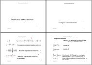
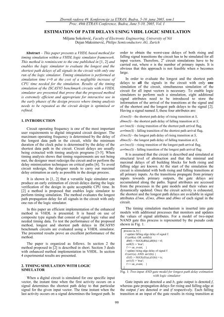
its output, but rising transition at an input is capable toproduce falling transition at the output only if risingtransition had previously arrived at the other gate input.Delay model <strong>of</strong> arbitrary complexity can be applied, takinginto account input signal slopes, loading capacitances andother parameters that influence ranges <strong>of</strong> gate <strong>delays</strong> tr andtf. Each time a delay attribute <strong>of</strong> output signal f is changed,an event must be scheduled to signal f with zero delay inorder to activate the processes performing the timing<strong>simulation</strong> in the gates driven by the NAND gate.To implement the timing <strong>simulation</strong> algorithm in <strong>logic</strong>simulator, a generalized signal attribute modeling mechanismis proposed in [2]. It is built in AleC++ hardware descriptionlanguage – the input language <strong>of</strong> Alecsis simulator [7]. InAleC++ user-defined signal attributes can be accessed andupdated in the processes during the <strong>simulation</strong>. Theexperimental results presented in [2] show that the proposedmethod is fast and appropriate for interactive use during <strong>logic</strong>verification.3. IMPLEMENTATION IN VHDLAlthough the user-defined signal attributes are availablein VHDL [87], they cannot be accessed and updated from theprocesses during the <strong>simulation</strong>. Therefore, a differentmodeling mechanism is necessary for the implementation <strong>of</strong>the timing <strong>simulation</strong> in VHDL simulator. We propose theuse <strong>of</strong> composite signals <strong>of</strong> the record type. Such acomposite signal consists <strong>of</strong> <strong>logic</strong> state and the timingattributes arr1mn, arr1mx, arr0mn, arr0mx, d1mn, d1mx,d0mn and d0mx. The record type DCSM_std_<strong>logic</strong> for the scalarsignals can be declared in VHDL as:type DCSM_std_<strong>logic</strong> is recordstatemn: std_u<strong>logic</strong>;d0mn: time;d1mn: time;arr0mn: boolean;arr1mn: boolean;statemx: std_u<strong>logic</strong>;d0mx: time;d1mx: time;arr0mx: boolean;arr1mx: boolean;end record DCSM_std_u<strong>logic</strong>;For the bus signals type DCSM_std_<strong>logic</strong>_vector can bedeclared as:type DCSM_std_<strong>logic</strong>_vector is array(natural range ) <strong>of</strong> DCSM_std_<strong>logic</strong>;Assuming the input and output signals <strong>of</strong> theDCSM_std_<strong>logic</strong> type, the complete model <strong>of</strong> a two-inputNAND gate can be described in VHDL as shown in Fig. 2.Processes labeled p1 and p2 are intended for standard <strong>logic</strong><strong>simulation</strong>. They model the <strong>logic</strong> function and delay function<strong>of</strong> the NAND gate. Processes labeled p3 and p4 are intendedfor the timing <strong>simulation</strong>. They monitor the timing attributes<strong>of</strong> gate inputs inp1 and inp2 and update the timing attributes<strong>of</strong> gate output oupt.Note that processes p3 and p4 are sensitive to the timingattributes <strong>of</strong> the input signals inp1 and inp2, but not to their<strong>logic</strong> states. Similarly, process p1 and p2 are sensitive toevents on input signal states, but not to their timing attributes.Hence, the two types <strong>of</strong> processes are independent. Logic<strong>simulation</strong> and timing <strong>simulation</strong> can be performedseparately or simultaneously.It is also important that the changes <strong>of</strong> the timingattributes <strong>of</strong> the output signal outp are always scheduled withzero delay in processes p3 and p4. If the timing <strong>simulation</strong> isinitiated at some time instant <strong>of</strong> <strong>simulation</strong> time, it will befinished at the same time instant, since the activity related totiming <strong>simulation</strong> is performed with no delay. We suggestthat timing <strong>simulation</strong> should be performed in initial timeinstant t=0 <strong>of</strong> <strong>simulation</strong>. If no timing attribute is changedduring the <strong>simulation</strong>, timing <strong>simulation</strong> is suppressed andthe simulator performs standard <strong>logic</strong> <strong>simulation</strong>. Timing<strong>simulation</strong> is invoked by setting the timing attributes arr1mn,arr1mx, arr0mn and arr0mx <strong>of</strong> primary inputs to value true. Ifthe primary inputs are grouped into a bus signal inp, thetiming analysis can be invoked by only one concurrent signalassignment command:inp ('0', 0 sec, 0 sec, true, true, '0', 0 sec, 0 sec, true, true));.Once the <strong>simulation</strong> time advances to t>0 sec, longest andshortest <strong>path</strong> <strong>delays</strong> <strong>of</strong> all signals in the circuit are availableand can be logged out. One additional process in the toplevelentity can be added that waits for some small timeperiod (for example, 1 pico second), prints the shortest andthe longest <strong>path</strong> <strong>delays</strong> to the screen or file, and thensuspends to the end <strong>of</strong> the <strong>simulation</strong>. An example <strong>of</strong> such aprocess is as follows:log: processbeginwait for 1 ps;--- print the timing analysis resultswait;end process log;entity nandg isgeneric (tpd_hlmn : time := 0.95 ns;tpd_lhmn : time := 1 ns;tpd_hlmx : time := 0.9 ns;tpd_lhmx : time := 1.05 ns);port (out1 : out DCSM_std_<strong>logic</strong> := ('0', 0.0 sec, 0.0 sec, false,false, '0', 0.0 sec, 0.0 sec, false, false);in1, in2: in DCSM_std_<strong>logic</strong> := ('0', 0.0 sec, 0.0 sec, false,false, '0', 0.0 sec, 0.0 sec, false, false));end nandg;architecture only <strong>of</strong> nandg isbegin---- Logic function:p1: process(in1.statemn, in2.statemn)variable val,ex_value : std_<strong>logic</strong> := '0';beginval := in1.statemn and in2.statemn;val := not (val);if val /= ex_value thenex_value := val;case val iswhen '0' =>out1.statemn out1.statemn end case;end if;end process p1;p2: process(in1.statemx, in2.statemx)variable val,ex_value : std_<strong>logic</strong> := '0';beginval := in1.statemx and in2.statemx;val := not (val);if val /= ex_value thenex_value := val;case val iswhen '0' =>out1.statemx out1.statemx end case;100
end if;end process p2;---- Timing <strong>simulation</strong>:p3: process (in1.d0mn, in1.d1mn, in1.arr0mn, in1.arr1mn,in2.d0mn, in2.d1mn, in2.arr0mn, in2.arr1mn)beginif (in1.arr0mn or in2.arr0mn) thenout1.d1mn
ISCAS'85 circuit, the <strong>simulation</strong> result was a list <strong>of</strong> d1 andd0, minimal and maximal parameters <strong>of</strong> all primary outputsignals. The maximal <strong>of</strong> these values is given in column D mx,while the minimal values are given in column D mn <strong>of</strong> Table 1representing the delay <strong>of</strong> the longest and the shortest <strong>path</strong>s inthe circuit.CircuitnameTable 1: Results <strong>of</strong> timing and <strong>logic</strong> <strong>simulation</strong> <strong>of</strong> ISCAS'85benchmark circuits with a VHDL simulatorNumber<strong>of</strong>signalsNumber<strong>of</strong>inputsNumber<strong>of</strong>outputsNumber<strong>of</strong>gatesD[ns]D fmn[ns]D fmx[ns]D rmn[ns]D rmx[ns]c17 11 5 2 6 3 1.95 2.85 1.95 3c432 196 36 7 160 17 1.95 16.5 1.95 16.5c499 243 41 32 202 11 0.95 1125 1 11.4c880 443 60 26 383 24 5.8 23.4 5.9 23.7c1355 587 41 32 546 24 2.9 23.55 2.95 23.25c2670 1426 233 140 1193 32 4.9 31.65 4.85 31.2c3540 1719 50 22 1669 47 13.7 46.2 13.5 46.95c5315 2485 178 123 2307 49 3.95 48.3 3.85 47.25c6288 2448 32 32 2416 124 4.85 120.9 4.9 120.9c7552 3719 207 108 3512 43 5.9 41.85 5.8 42To estimate the additional CPU time consumed by thetiming <strong>simulation</strong> during the simulator run, the ISCAS'85circuits are also simulated <strong>using</strong> standard <strong>logic</strong> packageieee.std_<strong>logic</strong>_1164. Signals <strong>of</strong> type std_<strong>logic</strong> and std_<strong>logic</strong>_vectorwere used in this experiment. Since timing <strong>simulation</strong> in thefirst experiment is finished at t=2 picoseconds, the <strong>logic</strong><strong>simulation</strong> in the second experiment is also finished at t=2picoseconds. Timing <strong>simulation</strong> does not increasesignificantly the total CPU time.5. CONCLUSIONDuring the design process <strong>of</strong> digital integrated circuits itis extremely important to estimate the longest and theshortest <strong>path</strong> <strong>delays</strong> as early as possible. Design verificationis one <strong>of</strong> the early phases in the design process. It is usuallyperformed <strong>using</strong> a <strong>logic</strong> simulator to verify that the circuitmeets the required <strong>logic</strong> function and a timing simulator toverify that the circuit meets the required timingspecifications. The method proposed in this paper combinesthese two tools into one by enabling the VHDL simulator toperform the timing <strong>simulation</strong>. In this way the design processis simplified and accelerated.The problem <strong>of</strong> introducing <strong>of</strong> the timing <strong>simulation</strong> intothe VHDL simulator is solved by the use <strong>of</strong> signals <strong>of</strong> recordtype in VHDL. Additional timing data is associated with eachsignal and used only when the timing <strong>simulation</strong> is requested.Eight timing attributes are added to each signal.Extra memory for storing the timing attributes isproportional to the total number <strong>of</strong> signals in the circuit. Forsimulated ISCAS'85 circuits this number is less than 4000.Even if very complex circuits with millions <strong>of</strong> signals shouldbe simulated, the required extra memory would be <strong>of</strong> theorder <strong>of</strong> only tens <strong>of</strong> Mbytes. Storing memory is not a criticalissue and the simulator performance should not be affectedby the memory requirements.The experimental results also indicate that extra<strong>simulation</strong> CPU time due to timing <strong>simulation</strong> is almostnegligible for ISCAS'85 circuits. Timing <strong>simulation</strong> affectsonly the initialization phase <strong>of</strong> the <strong>simulation</strong>, whereas therest <strong>of</strong> the <strong>simulation</strong> flow usually takes the most <strong>of</strong> the CPUtime. The proposed method is simple for implementation andlibraries <strong>of</strong> gate models used in semi-custom designmethodologies.REFERENCES[1] D. M. Maksimović, V. B. Litovski, "LogicSimulation Methods For Longest Path DelayEstimation", IEE Proc.-Comput. Digit. Tech., Vol.149, No. 2, March 2002.[2] D. M. Maksimović, V. B. Litovski, "Tuning <strong>logic</strong>simulators for timing analysis", Electronics Letters,Vol. 35, No. 10, pp. 800-802, Stevenage, UK, May1999.[3] J. K. Ousterhout, "CRYSTAL: A Timing Analyzerfor NMOS VLSI Circuits", Proc. 3rd Caltech Conf.on VLSI, pp. 57-69, March 1983.[4] N. Jouppi, "TV: An NMOS Timing Analyzer", Proc.3rd Caltech Conf. on VLSI, pp. 71-85, March 1983.[5] C. Oh, M.R. Mercer, "Efficient Logic-Level TimingAnalysis Using Constraint-Guided Critical PathSearch", IEEE Trans. on VLSI Systems, Vol. 4, No.3, September 1996, pp. 346-355.[6] B. Hoppe, G. Neuendorf, D. Schmitt-Landsiedel, W.Specks, "Optimization <strong>of</strong> High-Speed CMOS LogicCircuits with Analytical Models for Signal Delay,Chip Area, and Dynamic Power Dissipation", IEEETrans. CAD, Vol. 9, No. 3, pp. 236-247, March1990.[7] Ž. Mrčarica, D. Glozić, V. Litovski, D. Maksimović,T. Ilić, D. Gavrilović, Alecsis 2.3 - the simulator forcircuits and systems, User's manual, Laboratory forElectronic Design Automation (<strong>LEDA</strong>), University<strong>of</strong> Niš, Faculty <strong>of</strong> Electronic Engineering, 1/1998,Niš, Yugoslavia (http://leda.elfak.ni.ac.yu)[8] IEEE-Std. 1076, 1993 Language Reference Manual[9] E. Brglez, H. Fujiwara, "A Neutral Netlist <strong>of</strong> 10Combinational Benchmark Circuits And a TargetTranslator in FORTRAN", Int. Symp. on Circuits andSystems, pp. 1929-1934, Kyoto, Japan, June 1985.[10] Active-HDL, ver. 5.1, ALDEC Inc., 2003.Sadržaj – U ovom radu predložen je metod analizekašnjenja korišćenjem VHDL simulatora. Ovaj metod jenadgradnja onih objavljenih u [1, 2], i omogućavasumulatoru da odredi minimalna i maksimalna kašnjenja svihputeva u kolu, i to izvršavanjem samo jedne simulacije ukolu. Vremenska analiza se izvršava u trenutku t=0, i samoneznatno produžava procesorsko vreme potrebno zasimulaciju. Da bi se verifikovala efikasnost predloženogmetoda, prikazani su i rezultati simulacije ISCAS'85benchmark kola, korišćenjem VHDL simulatora. Ovaj metodizuzetno je pogodan u ranim fazama procesa projektovanjagde je potrebno ponavljati vremensku analizu uvek kada sekolo optimizuje ili redizajnira.PROCENA KAŠNJENJA LOGIČKOG PUTAKORIŠĆENJEM VHDL LOGIČKE SIMULACIJEMiljana Sokolović and Dejan Maksimović102