Fast Spectroscopic Ellipsometer - ULVAC Technologies
Fast Spectroscopic Ellipsometer - ULVAC Technologies
Fast Spectroscopic Ellipsometer - ULVAC Technologies

Create successful ePaper yourself
Turn your PDF publications into a flip-book with our unique Google optimized e-Paper software.
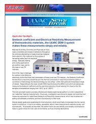
Application Spotlight...<br />
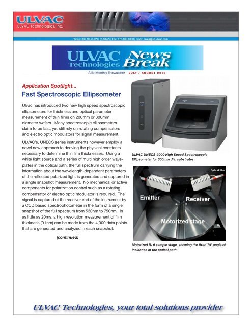
<strong>Fast</strong> <strong>Spectroscopic</strong> <strong>Ellipsometer</strong><br />
Ulvac has introduced two new high speed spectroscopic<br />
ellipsometers for thickness and optical parameter<br />
measurement of thin films on 200mm or 300mm<br />
diameter wafers. Many spectroscopic ellipsometers<br />
claim to be fast, yet still rely on rotating compensators<br />
and electro optic modulators for signal measurement.<br />
<strong>ULVAC</strong>’s, UNECS series instruments however employ a<br />
novel new approach to deriving the physical constants<br />
necessary to determine thin film thicknesses. Using a<br />
white light source and a series of multi high order waveplates<br />
in the optical path, the full spectrum carrying the<br />
information about the wavelength-dependant parameters<br />
of the reflected polarized light is generated and captured in<br />
a single snapshot measurement. No mechanical or active<br />
components for polarization control such as a rotating<br />
compensator or electro optic modulator is required. The<br />
signal is captured at the receiver end of the instrument by<br />
a CCD based spectrophotometer in the form of a single<br />
snapshot of the full spectrum from 530nm to 750nm. In<br />
as little as 20ms, a high resolution measurement of film<br />
thickness (0.1nm) can be made from the 4,000 data points<br />
that are generated and analyzed in each snapshot.<br />
(continued)<br />
JULY / AUGUST 2012<br />
<strong>ULVAC</strong> UNECS-3000 High Speed <strong>Spectroscopic</strong><br />
<strong>Ellipsometer</strong> for 300mm dia. substrates<br />
Motorized R- 0– sample stage, showing the fixed 70° angle of<br />
incidence of the optical path
It corresponds to the substrate size to<br />
1100mm x 1400mm. The substrate can<br />
be Load /Unload by MGV.<br />
> Color Mapping of Film Thickness Distribution<br />
News News<br />
Break<br />
a-Si/µc-Si Tandem Solar Cell Manufacturing Process<br />
The 300mm diameter wafer moves automatically under the optical path via an R-0- stage. In addition, the<br />
Z-height Substrate range (0 Substrate – 30mm) is ID adjusted TCO Laser automatically. Insulation Thanks Substrate to the PE-CVDhigh<br />
speed PE-CVD measurement a-Si/µc-Si Laser of PVD the instrument,<br />
Metal Laser<br />
Loading Cleaning Marking Patterning Tester Cleaning System 1 System 2 Patterning System Patterning<br />
and the high speed motion and compact design of this rotating sample stage, a high resolution film thickness<br />
distribution map of a 300mm Laser Patterning wafer<br />
can be performed (106 points) in as<br />
little as 120s. Thickness maps can<br />
Laser Patterning<br />
Laser Patterning<br />
be produced in X-Y or R-0- displays as<br />
shown at right.<br />
Metal Scribe<br />
TCO Glass Substrate TCO Laser Scribe a-Si Deposition µc-Si Deposition a-Si/µc-Si<br />
Laser Scribe<br />
Backside<br />
Electrode<br />
• 3D Profiler<br />
• 3D Profiler<br />
• Stylus Profiler<br />
• <strong>Ellipsometer</strong><br />
• Resistance<br />
• Crystallization Rate<br />
• 3D Profiler<br />
• Stylus Profiler<br />
• Resistance<br />
> Compact Design<br />
The size of the sensor unit is very<br />
a function that can evaluate optical characteristics in addition to the conventional measurement of deposition<br />
small due to the use of high order<br />
thickness, surface shapes, and resistance.<br />
wavelength plates. The built in light Color maps showing film thickness distribution across 300mm diameter wafers<br />
source The MPEC-1300 and controller Multi-Probe are mounted Evaluation of Thin-Film Characterization System for tandem type solar cell<br />
into has a the well following designed conventional compact enclosure. measuring The functions: CCD spectrophotometer (1) a “Surface Profiler,” is also which a very measures compact the component. deposition All<br />
these thickness elements and help in-plane to make distributions the UNECS of electrode-use system smaller, thin less films; expensive, (2) a “Low-resistance and more reliable measurement,” than competitive which<br />
instruments. evaluates the resistance distributions of electrode-use metal thin films. In addition, four additional measuring<br />
functions have been intergraded including;<br />
> (3) Built-in a “Raman Type Spectroscopy,” which maps in-plane distributions by<br />
Because the components that make<br />
obtaining µc-Si Crystallinity; (4) a “Three-dimensional (3D) measurement,” which three-dimensionally evaluates<br />
up this ellipsometer are so small and<br />
the shapes both of film surfaces after laser scribing and of TCO (Transparent Conductive Oxide) film surfaces;<br />
compact, it’s possible to design this<br />
(5) a “<strong>Spectroscopic</strong> <strong>Ellipsometer</strong>,” which evaluates the optical constants of a-Si thin films; and (6) a “High-<br />
equipment directly into production<br />
resistance measurement,” which evaluates the high-resistance distributions of a-Si thin films. By including a<br />
tools for in-situ measurement of<br />
total of six types of measuring functions, the MPEC-1300 Multi-Probe Evaluation of Thin-Film Characterization<br />
thin film thickness or other optical<br />
System for tandem type solar cell has enabled the thin-film characteristics evaluation of tandem type thin-film<br />
properties.<br />
solar cells to be performed in one system. The optical In addition, components since inside all surface the UNECS areas can of be a installed glass substrate directly into up other to the<br />
The 5.5th-generation business end [the size components]<br />
can be measured production with the tools system, for enabling there is in-situ, no need in-line to film destroy thickness substrates measurements.<br />
for evaluation.<br />
of These the optical excellent system features are very can easy greatly reduce initial introduction costs and running costs by about 1/2 com-<br />
to pared locate to inside when other introducing instruments. two or Because more individual the measurement dedicated-use speed measuring of this unit instruments. is so fast and sensitive, this<br />
ellipsometer has the potential to be used as a real-time feedback control instrument for film thickness and quality<br />
control This evaluation purposes system in other is process designed tools such and that equipment. the user can Integrated select the metrology measuring using functions an ellipsometer to be included for real time<br />
in-tool according film thickness to the user’s measurements purpose. <strong>ULVAC</strong> can provide is also significant developing advantages a system for and evaluating cost savings the distributions for manufacturers. of TCO<br />
Haze and solar cell local conversion efficiency.<br />
> The Demo newly and released Sampling MPEC-1300 Work tandem type thin-film solar cell hybrid thin-film characteristics evaluation<br />
system will be available starting from June 24, 2009. For further information, please contact us.<br />
<strong>ULVAC</strong> offers sampling of customer supplied substrates at our facility. Sampling data and a detailed discussion<br />
of those results can be provided. And training is available at customer facilities or in our lab in Methuen, MA.<br />
For Further Information, Please Contact Us...<br />
Contact Us<br />
• 3D Profiler<br />
• Stylus Profiler<br />
<strong>ULVAC</strong> <strong>Technologies</strong>, your total solutions provider