3-axis magnetometers using spin dependent tunneling: reduced ...
3-axis magnetometers using spin dependent tunneling: reduced ...
3-axis magnetometers using spin dependent tunneling: reduced ...

You also want an ePaper? Increase the reach of your titles
YUMPU automatically turns print PDFs into web optimized ePapers that Google loves.
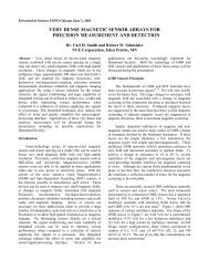
This is a preprint version of a paper published in: Proceedings of SPIE, Vol. 5090 (2003), p.208-213.layers of Al metal for interconnection and integrated planar coils, the SDT devices themselves, and some plated NiFeflux concentrators. Once the wafers are finished, they are diced and sent to a packaging house where they are diced,wire bonded, and molded into standard integrated circuit packages. A diagram and photograph of a finished SDT sensorchip is shown below in Figure 3. Automated testing of packaged parts allows for rapid winnowing away of lesserperformingparts. The SDT parts are mounted on and soldered to a printed circuit board just like any other chip. Themagnetic operation of the sensors is described elsewhere (SPIE AeroSense 2002) 3 .Pin 8Pin 7Pin 6Pin 5V +OUT +OC -OC+top down viewBridgeR4R3R1R2NVE(100141)ParallelField CoilOC1OC2OrthogonalField Coilsensitive<strong>axis</strong>PC2PC1OUT-V -PC -PC +Pin 1Pin 2Pin 3Pin 1Figure 3. The drawing on the left shows schematically the components that are contained within the SDT sensor package. Thephotograph on the right is of an SDT sensor die packaged in an SOIC-8-pin package. The package material in this case is clear, whichallows one to see the die, wirebonds, and bonding pads of the finished device.3. PERFORMANCEThis section will discuss the performance of the 3-<strong>axis</strong> SDT magnetometer in terms of power, and noise. The SDTtransducer itself has the greatest influence on both power and noise. The SDT transfer curve, a plot of Output Voltagevs. Magnetic Field, is described in section 3.1. The noise performance of the board is described in section 3.2. Then arediscussed the power and overall specifications for the board.1. Transducer Transfer CurveThe SDT low-power transducer curve has been evolving towards an ideal shape over the past several years. In this case,“ideal” means a wide range of field over which the output is linear with little or no hysteresis. Further, the transfer curveshould be centered on zero field and zero volts. The curve shown in Figure 4 below comes close to this ideal. There isstill some hysteresis and offset. The offset occurs both in voltage and field. The voltage offset is from a mismatch of theresistors in the transducer bridge (offset of .05 Volts out of 5V excitation = 1%offset). The field offset is a function ofthe sensor’s magnetic design. There are efforts underway to continue reducing these non-idealities. The transducerscome in two designs, a 60 kOhm (6 Volt max) and a 300 kOhm (12 Volt max). These designs vary in the number andsize of the tunnel junctions that make up the resistance bridge.