RFIC Layout Analysis Using Sonnet EM with ... - Sonnet Software
RFIC Layout Analysis Using Sonnet EM with ... - Sonnet Software
RFIC Layout Analysis Using Sonnet EM with ... - Sonnet Software
- No tags were found...

You also want an ePaper? Increase the reach of your titles
YUMPU automatically turns print PDFs into web optimized ePapers that Google loves.
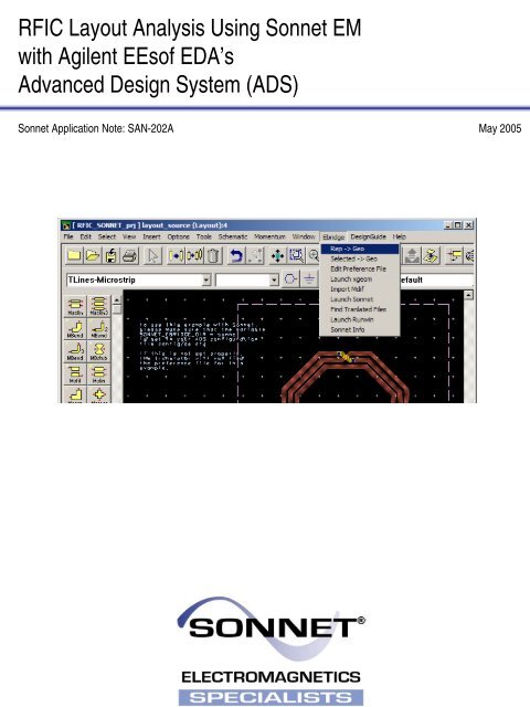
<strong>RFIC</strong> <strong>Layout</strong> <strong>Analysis</strong> <strong>Using</strong> <strong>Sonnet</strong> <strong>EM</strong><strong>with</strong> Agilent EEsof EDA’sAdvanced Design System (ADS)<strong>Sonnet</strong> Application Note: SAN-202A May 2005
Description of <strong>Sonnet</strong> Suites Professional<strong>Sonnet</strong> Suites Professional is an industry leading full-wave 3D Planar Electromagnetic (<strong>EM</strong>) field simulationsoftware based on the Method of Moment (MoM) technique which accounts for all coupling and radiationeffects from DC to THz. It also takes full advantage of mathematically robust and reliable FFT formulationwhich avoids time consuming, error prone numerical integration. Both MoM and FFT combined gives <strong>Sonnet</strong>an added assurance that it will give outstanding accuracy every time on problems that have traditionally beendifficult to solve. Problems <strong>with</strong> high dielectric constant, thin dielectric layers and/or small dimensions <strong>with</strong>respect to the wavelength are handled especially well <strong>with</strong> <strong>Sonnet</strong>. <strong>Sonnet</strong> continues to be an indispensabletool for designers involved in RF/Microwave circuits such as distributed filters, transitions, Low TemperatureCo-fired Ceramics, multi-layer RF packages, coplanar waveguides, and antennas. In addition, <strong>Sonnet</strong> hasproven successful in mm-wave designs as well as in <strong>EM</strong>C and <strong>EM</strong>I analysis.<strong>Sonnet</strong> Professional Key Benefits• Accurately model passive components (inductors, capacitors, resistors) to determine values like RLC and Qfactor• Accurately model multi layer interconnects and via structures• Generate a technology accurate electrical model for arbitrary layout shapes• Quantify parasitic coupling between components, interconnects and vias• Include substrate induced effects like substrate loss and eddy currents• Visualize the current flow in components, interconnects and vias<strong>Sonnet</strong> Professional Key Features• FFT based Method of Moments analysis for ultimate reliability and accuracy• Easy to learn, easy and efficient to use• Only one high precision analysis engine – no need to switch between solvers• Patented Conformal Meshing strategy for very efficient high accuracy meshing of curved structures• Finite thickness modelling (including advanced N-sheet model)• Dielectric bricks for truncated dielectric materials (e.g. MIM capacitor)• Adaptive Band Synthesis for fast and reliable frequency sweeps <strong>with</strong> a minimum number of <strong>EM</strong> samples - moreefficient than traditional approaches• Easy to use data display for analysis results, including R, L, C, Q evaluation• Equation capability for pre-defined or customized calculation on simulated data• All configuration and technology setup is menu / dialog based– no need to edit configuration text files• Remote simulation capability• Compatible <strong>with</strong> the LSF cluster and load balancing system• Seamless integration <strong>with</strong> Cadence ® Virtuoso ® , Agilent EEsof EDA’s ADS, AWR ® Microwave Office ® andAnalog Office and Eagleware-Elanix GENESYS design environments• <strong>Sonnet</strong> <strong>Software</strong> Inc. is a Cadence Connections partner2
IntroductionThe <strong>Sonnet</strong> Professional electromagnetic analysis program offers a menu level integration into the ADS design environment. This interface,called Ebridge allows the <strong>RFIC</strong> designer to take layouts very easily from ADS to <strong>Sonnet</strong> for high precision <strong>EM</strong> analysis, and back annotateresults. Material and technology information will be extracted from schematic MSUB blocks, or from a project technology file.In this document, we will study the data transfer and simulation setup of a layout-only project, <strong>with</strong> no circuit models. We base oursymmetrical inductor example on the following sample technology:air εr=11µm1µm2µmMetal M1 σ=3e7S/m ADS: cond (1)via ADS: via(39) oxide εr=3.9 cond= 0S/mMetal M2 σ=3e7S/m ADS: cond2 (2)2µm300µm substrate εr=11.9 cond= 5S/m3
When to Use <strong>Sonnet</strong> Professional <strong>Analysis</strong>The use of electromagnetic analysis <strong>with</strong> <strong>Sonnet</strong> Professional is especially valuable in the following design situations:When parasitic coupling is present.Parasitic coupling is not always easy to predict <strong>with</strong>out using electromagnetic analysis. Even elements which are "sufficiently" far apart cansuffer from parasitic coupling: inductive or capacitive coupling, resonance effects due to grounding and surface waves that might propagateat the substrate boundary under certain conditions. <strong>Sonnet</strong> Professional analysis is based on the physical properties of your technology andwill account for such physical effects.When accurate circuit models are not available or circuit model parameters are out of range.Model based circuit simulators are based on models for a specific application, <strong>with</strong> limited parameter range. For example, only selectedgeometries, substrate types and substrate parameters are available. It is difficult to estimate the error induced by parameter extrapolation,so using models outside their designed parameter range is not suitable for critical applications.Whenever a layout feature cannot be described by a circuit model, due to its geometry or technology, the physics based analysis <strong>with</strong><strong>Sonnet</strong> Professional will provide the answer. An example for this could be a special inductor, capacitor or transformer which is not includedin the design kit. <strong>Sonnet</strong> can be used to analyze those components "on the fly", or generate a full library of components models <strong>with</strong>trustworthy electrical results.<strong>Sonnet</strong> Plug-in for ADS: Ebridge<strong>Sonnet</strong> offers a menu level integration into the ADS environment through the “Ebridge” plug-in. This is an add-on from <strong>Sonnet</strong> <strong>Software</strong>which requires a license.The Ebridge menu is loaded into ADS as described in the <strong>Sonnet</strong> Installation Manual in chapter “Configuration Procedure for the AgilentInterface”. In this example, we assume that the ADS variableSONNET_EBRIDGE_DIR = sonnetis also defined in the ADS configuration file de.cfg to specify a subdirectory /sonnet <strong>with</strong>in the ADS project directory, where the <strong>Sonnet</strong>preference file and the <strong>Sonnet</strong> simulation models and results are located.When activated, the ebridge menu appears in both the ADS Schematic and <strong>Layout</strong> windows, as illustrated below.Ebridge Menu <strong>with</strong>in Agilent ADS4
What is the “Ebridge preference file”In our example, we use a layout translation <strong>with</strong> no reference to a circuit simulation schematic. Thus, we cannot get substrate and metalinformation from an MSUB[1] schematic element, and need to get all physical material information from a “preference” file.In our example, we will use the preference file to define the metal types and their use for different layers, the substrate materials andthickness (stack-up) and also some simulation settings like frequency range and cell size (<strong>EM</strong> simulation spatial sampling resolution).In this document, we will only give a brief description of the settings used. A detailed description of Ebridge and the preference file entriescan found in the <strong>Sonnet</strong> User’s Manual.[1] MSUB is just one example here. Ebridge also supports many other substrate blocks.To edit the preference file, select the menu item Ebridge > Edit Preference File.Here is the file that we use for the technology in this example:Level 0Level 2Level 4SIZE_X_CELL 2SIZE_Y_CELL 2EXT 100CUSTOM_SUBCLAYER 2000 1 1 0 0 0 0 Air_aboveCLAYER 2 3.9 1 0 0 0 0 Oxide_above_M1CLAYER 1 3.9 1 0 0 0 0 Oxide_at_M1CLAYER 2 3.9 1 0 0 0 0 Oxide_betweenCLAYER 1 3.9 1 0 0 0 0 Oxide_at_M2CLAYER 2 3.9 1 0 0 0 0 Oxide_below_M2CLAYER 300 11.9 1 0 0 5 0 SubstrateEND CUSTOM_SUB! SETUP METALIZATION LOSS! Thick metal model, 3e7S/m, 1 micron, 2 sheetsMET "M1" TMM 37000000 0 1 2MET "M2" TMM 37000000 0 1 2! ignore layer # 37 (Momentum Box)LAYER 37 IGNOREthicknessεr σ Name! MAP METALIZATION LAYERS! ADS layer 1 to <strong>Sonnet</strong> level 2, material index 0 -> M1! ADS layer 2 to <strong>Sonnet</strong> level 4, material index 1 -> M2LAYER 1 2 0LAYER 2 4 1simulation cell size is2µmDielectric layersfrom top to bottommetal types,used by index,starting <strong>with</strong> 0! BOUNDING BOX TO BOX BOTTOMLAYER 13 GND -1! MAP VIA LAYERS! ADS layer 39 to <strong>Sonnet</strong> level 3, material index -1 -> losslessLAYER 39 3 -1 VIA! SETUP REFERENCE PLANES! number of substrate heights to add to each side of circuitEXT 0! ANALYSIS FREQUENCY SWEEP in GHzFREQSABS_ENTRY 0.50 20DC_FREQ AUTOEND FREQSdrawing layersmapping and metaltype assignmentlossless = index -1we use this to set the <strong>Sonnet</strong> box size(bounding box)via layermapping and metaltype assignmentanalysis setupfrequency range5
Definition for thick metal analysisIn the preference file shown here, thick metal types are defined. Many <strong>RFIC</strong> technology components contain transmission lines and otheradjacent metal traces <strong>with</strong> narrow gaps that are on the order of the metal thickness. In these cases electromagnetic analysis <strong>with</strong> true thickmetal analysis will provide more realistic simulation results. For this reason, our example is based on thick metal analysis. For a discussion ofthin metal vs. thick metal, please refer to the <strong>Sonnet</strong> User's Guide, Chapter 19: Thick Metal.Create the <strong>Sonnet</strong> simulationmodel from ADSTo create a <strong>Sonnet</strong> simulation model filefrom the current layout view, select themenu item Rep -> Geo from the Ebridgemenu. This will create the <strong>Sonnet</strong> <strong>EM</strong>simulation model and show a messagewhen the file was written successfully.Now, you can open the <strong>Sonnet</strong> <strong>EM</strong>simulation model file in the <strong>Sonnet</strong> projecteditor “xgeom”. To do so, select the menuitem Launch xgeom from the Ebridgemenu.The <strong>EM</strong> simulation model is almostcomplete now, except for the portconfiguration and a few advancedsimulation settings.Box and cell sizeThe <strong>EM</strong> analysis cell size was taken fromthe preference file (2µm in both directions)and the box size was set automaticallyduring data translation as the boundingbox of all translated objects. In our case,we had included the ADS layer 13 “bound”and mapped it to the bottom of theanalysis box in <strong>Sonnet</strong>. It has no effect on<strong>EM</strong> simulation; it only helps during datatransfer to set the bounding box asdesired, because it is the biggest layoutobject.For good results, the size of the analysisbox and the cell size must be configured<strong>with</strong> care. The cell size determines thespatial sampling resolution for the <strong>EM</strong>analysis engine, so this is the key to highprecision results. The box size must belarge enough to avoid coupling betweenthe circuit and the side walls. If you haveany questions on these issues, pleasecontact <strong>Sonnet</strong> support for the details.Box and cell size are set in the Circuit >Box dialog. If you change the box size andwant to move your circuit, you can do thiseasily by first doing Edit > Select All(+) and then moving the circuit<strong>with</strong> the mouse, or use Modify > Centerto center it horizontally and/or vertically inthe analysis box.6
Subsection typeFor <strong>EM</strong> analysis of <strong>RFIC</strong> inductors,<strong>Sonnet</strong>’s new conformal meshingcapability is very useful, because itenables significant memory andsimulation time reductions for curvedand diagonal polygons. Please refer tothe <strong>Sonnet</strong> User's Guide for moreinformation about conformal meshing.You can enable conformal meshing perpolygon, but you can also do Edit>Select All and then change allpolygons at once: Modify > Metalproperties > Fill Type.Add portsOnce the <strong>EM</strong> Project geometry(including vias) is complete andmaterial properties are defined, theremaining step is to define ports. In<strong>Sonnet</strong>, different port types exist, butthe most common port type is the boxwall port. Box walls are well suited forinductor analysis because we can easilyand accurately de-embed the feed lineup to the desired reference plane.Calibration error for box wall ports in<strong>Sonnet</strong> have been shown to exhibitnumerical noise errors than better than100 dB down or more.To define a box wall port, you mustextend each feed line to a box wall.You can do so by adding a newpolygon, or by stretching an existingpolygon. One easy method to stretch:use the Tools > Reshape commandand drag a window around the edgethat you want to stretch. Then, use theModify > Snap to... command tosnap the edge to one of the box walls.To define a box wall port, use theTools > Add Port command and clickon the polygon edge where the feedline touches the box wall. This adds abox wall port at that location, <strong>with</strong> thepositive terminal connected to the feedline and the negative terminalconnected to the box (ground).7
Add Reference Planes(Optional)To compensate for the additional length ofthe feed line, a reference plane shift canbe applied by using the Circuit > Ref.Planes / Cal. Length. menu item. Adialog will be displayed where you canenter a reference plane shift for each sideof the box. The offset value can be a fixedvalue, or linked to a polygon vertex. Thevalue can be typed in or defined by a leftbutton mouse click at the desired location.If you need to define an internal portinside the box <strong>with</strong> no access to the boxwall, you can also use an "auto groundedport" which connects to groundautomatically (using a via which is addedat run time and goes down through alllayers until it touches the bottom of thebox). Auto grounded ports can be attachedto a polygon edge at any location insidethe box.We strongly recommend to use box wallports when you have lossy bulk layers!Auto grounded ports may give invalidresults <strong>with</strong> very lossy substrates.8
Run analysis to generateS-parameters and L/QplotsAfter setting up the simulation model, a typicalthick metal circular spiral inductor might look like:<strong>Analysis</strong> SetupTo set up analysis, use <strong>Analysis</strong> > Setup fromthe <strong>Sonnet</strong> xgeom menu. In most cases, anAdaptive Band Synthesis (ABS) sweep over awide frequency range will be the best choice, e.g.0.1 – 15GHz. This typically takes five or six <strong>EM</strong>simulated frequency points to generate fine dataoutput at approximately 300 frequency points inthe desired range 0.1-15GHz.Please don’t forget to enable the advanced solversetting “Q factor accuracy” to ensure that ABSresults are visually identical to a discretefrequency analysis for Q-factor values. (Requires<strong>Sonnet</strong> Version 10 or later)9
Plot <strong>Analysis</strong> DataElectromagnetic analysis <strong>with</strong> the exampleshown here will take 16 minutes and 59MBmemory to simulate the completefrequency range (full thick metal analysison P4/2.5GHz) <strong>with</strong> very fine geometrysampling of 2µm at 600µm box size.Plot EquationsWhen the <strong>EM</strong> simulation is done, you cannow use the new equation feature, whichplots results based on predefined or userdefined equations. <strong>Sonnet</strong> has alreadyincluded equations to plot the seriesinductance of two port devices (equationname inductance2) and the quality factor.To plot these values, bring up the result inthe emGraph data display, then useEquation > Add equation curve fromthe emGraph menu.Note: You can also plot results of differentequations on left and right axis at thesame time, or plot equation results as afunction of a swept parameter.10
View Current DensityIt is also interesting to observe the currentdensity as a function of frequency.Calculating the current density addsminimal <strong>EM</strong> simulation overhead, but it isvery useful to gain insight into how acircuit works and what cell size isappropriate.Current density at 0.1GHz is shown in thefigure to the right. Since skin effect at thislow frequency is much thicker than themetal, current is relatively evenlydistributed across the width of thetransmission lines, and the conductivelosses dominate the current spreadingeffects.Current density at 15GHz is shown in thesecond picture. In this case, skin effectlosses will dominate the spiral Q, as theskin effect is much thinner than the metal.In addition, current crowding is observedbelow (where current tends to have amaximum on the edges of thetransmission lines). Current crowdingoccurs at higher frequencies where theself-reactance of the transmission lines iscomparable to or greater than theconductive loss. Note the high edgecurrent that <strong>Sonnet</strong> conformal meshingshows very accurately. This edge currentmust be modeled very accurately by any<strong>EM</strong> analysis tool in order to correctlyassess the losses in the device thatcontribute to the Q.Back annotating results to ADSYou can easily back annotate <strong>EM</strong> simulation results to ADS, to use it in a model based simulation. In the <strong>Sonnet</strong> plotting tool emGraph,select the data set which you want to export, then use Output > S/Y/Z Parameter File from the menu. This brings up a dialogwhere you can save model data in Touchstone (S2P), MDIF and other file formats. That data can be used easily in ADS as black boxdata, just like measurement results.The Ebridge plug-in also offers a menu item Import MDIF to assist you in reading MDIF swept parameter results created by a sweptparameter<strong>EM</strong> analysis in <strong>Sonnet</strong> into an ADS schematic.11
This application note is courtesy of Dr.-Ing. Volker Muehlhaus ofMuehlhaus Consulting & <strong>Software</strong> GmbHwww.muehlhaus.com<strong>Sonnet</strong> <strong>Software</strong>, Inc.Phone: 315-453-3096Toll Free in North America: 877-7SONNETEmail: info@sonnetsoftware.comWeb: www.sonnetsoftware.comUnited States Regional Sales:Eastern US Sales Office: 203.439.0815Western US Sales Office: 303.443.2646Japan:<strong>Sonnet</strong> Giken Co., Ltd.Phone: 43-463-6663Email: info@mail.sonnetsoftware.co.jpWeb: www.sonnetsoftware.co.jpGermany:Muehlhaus Consulting & <strong>Software</strong> GmbHPhone: +49 (2302) 91438-0Email: info@muehlhaus.comWeb: www.muehlhaus.com12