IJIES-2008 VOLUME 1 ISSUE 1 - inass
IJIES-2008 VOLUME 1 ISSUE 1 - inass
IJIES-2008 VOLUME 1 ISSUE 1 - inass

You also want an ePaper? Increase the reach of your titles
YUMPU automatically turns print PDFs into web optimized ePapers that Google loves.
International Journal ofIntelligent Engineering & Systemshttp://www.<strong>inass</strong>.org/Analysis of a 2 ¢/ 1.5 ¢/ 1¢ Mode DC-DC Converter Designed by UsingSwitched-Capacitor TechniquesKei Eguchi ½ , Takahiro Inoue ¾ , Ichirou Oota ¿ , Hongbing Zhu , Fumio Ueno ½ Department of Technology Education, Shizuoka University,836, Ohya, Shizuoka, 422-8529, Japan¾ Department of Electrical and Computer Engineering, Kumamoto University,2-40-1, Kurokami, Kumamoto, 860-8555, Japan¿ Department of Information and Communication, Kumamoto National College of Technology,2659-2, Suya, Koushi, Kumamoto, 861-1102, Japan Department of Computer Science, Hiroshima Kokusai Gakuin University,6-20-1, Nakano, Akiku, Hiroshima, 739-0321, Japan Department of Software Science, Sojo University,4-22-1, Ikeda, Kumamoto, 860-0082, JapanAbstract: For mobile applications, a switched-capacitor (SC) DC-DC converter which offers a 2 ¢/ 1.5 ¢/1¢ modeof operation is presented, and its properties are analyzed theoretically in this paper. Aimed at backlighting applications,battery applications, etc., the proposed converter provides stepped-up/stepped-down voltages. Compared with theconventional approaches employing doubler circuits, the proposed converter can realize high efficiency and flexibilityof output voltages. The validity of the proposed converter is confirmed by SPICE simulations and theoretical analyses.Concerning the power efficiency and the optimal duty factor, the confirmation result shows that the theoretical resultscorrespond to the simulation results well. Furthermore, under the conditions that the input voltage Î Ò =3.7 V, theoutput load Ê Ä ¿¼Å, and the output voltage Î ÓÙØ 3.3 5.3 V, the proposed converter can improve the powerefficiency more than twice from that of the conventional circuit.Keywords: DC-DC converters; Switched-capacitor circuits; Backlighting applications; Versatile converters;Discrete-time circuits1. IntroductionRecently, according to the down-scaling of portableelectronic products, power converters designed by usingswitched-capacitor (SC) techniques [1-16] attractmuch attention. Since no magnetic elements are requiredto design the SC power converters, they canrealize thin circuit composition, light-weight and low-½ Corresponding author.Email address: ekeguch@ipc.shizuoka.ac.jpnoise. For this reason, the SC power converter is usedas a driver circuit of white LEDs for display backlighting,a building block of battery management systems,and so on. For example, in mobile backlighting applications,the stepped-up voltage such as Î(Typ. = 5 V) is required to drive some LEDs at upto 25 mA. On the other hand, to extend the batterylife, versatile SC converters which can provide stepup/step-downvoltages are necessary.International Journal of Intelligent Engineering and Systems 1 (<strong>2008</strong>) 1-8 1
VoutVoutΔq Τ1,VoutS2,3 S2,4C 3C 3Φ1,iΦ2,jVinTS1,1S2,1S2,2S1,2C 1 C 2T1T2S1,3Figure 1. Proposed SC DC-DC converter.ttΔq Τ1,VinRon Ron RcntVinRonΔq Τ2,VinC 1 C 2(a) ËØØ Ì ½VoutRon C 3C 1 C 2Δq Τ2,VoutVinRonTo adjust the output voltage, on-resistance controlscheme [9,12,13,16] or pulse width modulation (PWM)scheme [10, 11] is usually employed in the SC DC-DC converter, because the ratio of the voltage conversionis predetermined by circuit structure. The powerefficiency of the SC power converters gets worse bythe regulation of the output voltage. In the case of avoltage doubler circuit [14-16], for example, the efficiencydecreases greatly when the low output voltageis required, because the output voltage must be regulatedstrongly. To solve this problem, we proposedthe circuit topology of a 1.5 ¢ mode SC DC-DC converterin [9], because it is necessary to create a 5 Vpower supply 1 from a 3.7 V supply of a lithium-ionbattery. However, by changing the control scheme ofclock pulses, fortunately, the converter proposed in [9]can work as a versatile step-up/step-down converterwhich can offer a 2 ¢/ 1.5 ¢/ 1¢ mode of operation.As mentioned above, to extend the battery life,the step-up/step-down converters are useful.In this paper, aimed at backlighting applications,battery management applications, etc., the converterproposed in [9] is modified to provide stepped-up /stepped-down voltages, and the handy theoretical formulasare given concerning the power efficiency andthe optimal duty factor. Compared with the conventionalversatile converters based on doubler circuits[16], the proposed converter can realize high efficiencyand flexibility of output voltages, because it offers a 2¢/ 1.5 ¢/ 1¢ mode of operation. To confirm the validityof the circuit design and the theoretical analyses,SPICE simulations are performed.½ The typical voltage for backlighting applications is 5 V.Φ1,1 , Φ1,2 , Φ1,3Φ2,1 , Φ2,2 , Φ2,3 , Φ2,4Ron(b) ËØØ Ì ¾TT1T2(c) Timing of pulsesFigure 2. Instantaneous equivalent circuitswhen 1.5 ¢ mode of operation.2. Circuit StructureFigure 1 shows a 1.5 ¢ mode DC-DC converter designedby using the SC technique [9]. The converterconsists of 7 power switches and 3 capacitors. InFig.1, the power switches Ë ½ and Ë ¾ ´´ ½¿µand ´ ½µµ are driven by 2-phase clock pulses¨½ and ¨¾ , respectively. The interval of ¨½ and¨¾ is set to as follows:Ì Ì ½·Ì ¾Ì ½ ÌÒ Ì ¾ ´½ µÌ (1)where Ì is a period of the clock pulse and denotesa duty factor. By controlling the power switches Ë ½and Ë ¾ , the converter performs a DC-DC conversion.The control scheme and the circuit properties for a2 ¢/ 1.5 ¢/ 1¢ conversion will be described in thefollowing section.3. Theoretical Analysis3.1 1.5 ¢ ModeFirst, the equivalent circuit when a 1.5 ¢ mode isanalyzed. In the theoretical analysis, we assume thatttInternational Journal of Intelligent Engineering and Systems 1 (<strong>2008</strong>) 1-8 2
1. parasitic elements are not effective and 2. the timeconstant is quite larger than a period of the clock pulse.Figure 2 shows the instantaneous equivalent circuitsin the case of the 1.5 ¢ mode. In the steady state, thedifferential values of the electric charges in ´ ½ ¾ ¿µ satisfyI inVin1 : MI outRSCVo VoutFigure 3. General form of equivalent circuit.¡Õ Ì ½ ·¡Õ Ì ¾ ¼ (2)where ¡ÕÌ ½ and ¡Õ Ì ¾denote the electric charges whenËØØ Ì ½ and ËØØ Ì ¾, respectively. In the caseof ËØØ Ì ½, the differential values of the electriccharges in the input and the output terminals, ¡Õ Ì ½ÎÒand ¡Õ Ì ½ÎÓÙØ , are given by¡Õ Ì ½ÎÒ ¡ÕÌ ½ ½ ¡Õ¾ Ì ½Ò ¡Õ Ì ½ÎÓÙØ ¡Õ Ì ¿ ½ (3)Here, a general equivalent circuit of SC power converters[3,4,9,12] can be given by the circuit shown inFig.3, where Ê Ë is called an SC resistance, Å is aratio of the ideal transformer, and Î Ò and Î ÓÙØ denotean averaged input voltage and an averaged output voltage,respectively. The consumed energy Ï Ì of Fig.3can be expressed byOn the other hand, in the case of ËØØ Ì ¾, thedifferential values of the electric charges in the inputand the output terminals, ¡Õ Ì ¾ÎÒ and ¡Õ Ì ¾ÎÓÙØ , aregiven by¡Õ Ì ¾ÎÒ ´¡ÕÌ ½ ¾ ·¡Õ¾ Ì ¾ µÒ ¡Õ Ì ¾ÎÓÙØ ¡ÕÌ ½ ¾ ·¡Õ¾ Ì ¾ ·¡Õ¿ Ì ¾ (4)Here, the average currents of the input and the outputare given byÁ Ò ´¡Õ Ì ½ÎÒ ·¡Õ Ì ¾ÎÒ µÌ ¡Õ ÎÒ ÌÒ Á ÓÙØ ´¡Õ Ì ½ÎÓÙØ ·¡Õ Ì ¾ÎÓÙØ µÌ ¡Õ ÎÓÙØ Ì (5)where ¡Õ ÎÒ and ¡Õ ÎÓÙØ are the electric charges inthe input and the output, respectively. From Eqs.(2) (5), the following equation is derived:¿Á Ò Á ÓÙØ (6)¾In Fig.2, the energy consumed by resistors in oneperiod, Ï Ì , can be expressed bywhereÏ Ì Ï Ì ½ · Ï Ì ¾ (7)Ï Ì ½ ¾Ê ÓÒÌ ½ ´¡Õ½ Ì ½ µ¾ · ÊÒØÌ ½ ´¡Õ½ Ì ½ µ¾Ò Ï ¾Ê ÓÒ¾ÊÌ ¾ Ì ¾ ´¡Õ½ Ì ¾ µ¾ ÓÒ ·Ì ¾ ´¡Õ¾ Ì ¾ µ¾ From Eqs.(1) (5), Eq.(7) can be rewritten asÏ Ê ÓÒÌ ½ ¾Ì ´¡Õ Î ÓÙص ¾ · ÊÒØÌ ´¡Õ Î ÓÙص ¾Ê ÓÒÒ Ï Ì ¾ ´½ µÌ ´¡Õ Î ÓÙص ¾ (8)Ï Ì Ï Ì ½ · Ï Ì ¾¡Õ Î ÓÙØ ´ µ ¾ ¡ Ê Ë ¡ Ì (9)ÌBy substituting Eq.(8) into Eq.(9), the SC resistancewhen the 1.5 ¢ mode, Ê Ë¿¾ ,isgivenbyÊ Ë¿¾ ¾´½ · µ´½ µ ¡ Ê ÓÒ· ½ ´½ µ ¡ Ê ÒØ (10)The equivalent circuit of Fig.3 can be expressed bythe determinant using a Kettenmatrix. Therefore, byusing Eqs.(6) and (10), the equivalent circuit of theproposed converter is given by the following determinant: ÎÒ¾¿Á Ò¼¼¿¾½¼Ê Ë¿¾½ÎÓÙØÁ ÓÙØ (11)As Eq.(11) shows, the output voltage of the proposedcircuit becomes ´¿¾µÎ Ò when Ê Ë¿¾ Ê Ä .From Eq.(11), the averaged output voltage Î ÓÙØ isexpressed byÊ ÄÎ ÓÙØ ¡ ´ ¿Ê Ä · Ê Î Òµ (12)Ë¿¾ ¾Furthermore, the power efficiency ¿¾ 2 can be givenby¾Ê Ä Á ÓÙØ ¿¾ ¾ ¾Ê Ä Á ÓÙØ · ÊË¿¾ Á ÓÙØ ¾ Of course, the consumed energy of the peripheral circuits suchas pulse generators, comparators, etc. is disregarded in thepower efficiency of Eq.(13).International Journal of Intelligent Engineering and Systems 1 (<strong>2008</strong>) 1-8 3
Δq Τ1,VinVinΔq Τ2,VinVinΔq Τ1,VoutVoutC 3Ron Ron RcntC 2(a) ËØØ Ì ½Δq Τ2,VoutVoutRon C 3C 2Ron3.2 2 ¢ ModeFigure 4 shows the instantaneous equivalent circuitsin the case of a 2 ¢ mode. In Fig.4 (a), the differentialvalues of the electric charges, ¡Õ Ì ½ÎÒ and¡Õ Ì ½ÎÓÙØ , are given by¡Õ Ì ½ÎÒ ¡Õ ¾ Ì ½Ò ¡Õ Ì ½ÎÓÙØ ¡Õ ¿ Ì ½ (16)In Fig.4 (b), the differential values of the electric charges,¡Õ Ì ¾ÎÒ and ¡Õ Ì ¾ÎÓÙØ , are given by¡Õ Ì ¾ÎÒ ¡ÕÌ ¾ ¾Ò ¡Õ Ì ¾ÎÓÙØ ¡ÕÌ ¾ ¾ ·¡Õ¿ Ì ¾ (17)Φ2,1 , Φ1,2 , Φ1,3Φ2,2 , Φ2,4Φ1,1 , Φ2,3(b) ËØØ Ì ¾TT1T2(c) Timing of pulsesFigure 4. Instantaneous equivalent circuitswhen 2 ¢ mode of operation.Ê ÄÊ Ä · Ê Ë¿¾ (13)where Ê Ë¿¾ depends on the resistance Ê ÒØ shownin Eq.(10). As Eq.(13) shows, Î ÓÙØ can be regulatedby controlling Ê ÒØ which corresponds to the on-resistanceof Ë ½¿ (see in Fig.2.). In other word, the regulation isachieved by controlling the gate voltage of Ë ½¿ .As Eq.(13) shows, the increase of the Ê Ë¿¾ causesthe decrease of the efficiency ¿¾ . In other word, themaximum power efficiency is obtained when Ê ÒØ Ê ÓÒ . From Eq.(10), the minimum on-resistance ÑÒ´Ê Ë¿¾ µcan be expressed byÑÒ´Ê Ë¿¾ µttt´ ·¿µ´½ µ ¡ Ê ÓÒ (14)In Eq.(14), the optimum value of the parameter isobtained when ÑÒ´Ê Ë¿¾ µ¼ Ò ¼ ½ (15)From Eqs.(14) and (15), the optimal duty factor forthe 1.5 ¢ mode is ³ ¼ 3 .From Eqs.(2), (5), (16), and (17), the relation betweenthe input current and the output current is derived asÁ Ò ¾Á ÓÙØ (18)In Figs.4 (a) and (b), the energy consumed by resistorsin one period, Ï Ì ½ and Ï Ì ¾ , can be expressedbyÏ Ì ½ ¾Ê ÓÒÌ ½ ´¡Õ¾ Ì ½ µ¾ · ÊÒØÌ ½ ´¡Õ¾ Ì ½ µ¾Ò Ï Ì ¾ ¾Ê ÓÒÌ ¾ ´¡Õ¾ Ì ¾ µ¾ (19)respectively. From Eqs.(1), (2), (5), (16), and (17),Eq.(19) can be rewritten asÏ ¾Ê ÓÒÌ ½ Ì ´¡Õ Î ÓÙص ¾ · ÊÒØÌ ´¡Õ Î ÓÙص ¾¾Ê ÓÒ´½ µÌ ´¡Õ Î ÓÙص ¾ (20)Ò Ï Ì ¾ By substituting Eq.(20) into Eq.(9), the SC resistancefor the 2 ¢ mode, Ê Ë¾ , can be expressed byÊ Ë¾ ¾¡ Ê ÓÒ · ½´½ µ ¡ Ê ÒØ (21)Therefore, by using Eqs.(18) and (21), the equivalentcircuit is given by the following determinant: ÎÒÁ Ò ½¼ ½ ʾ˾ ÎÓÙØ (22)¼ ¾ ¼ ½ Á ÓÙØFrom Eq.(22), the averaged output voltage Î ÓÙØ isexpressed by¿ In other word, the power efficiency becomes the maximumvalue when ³ ¼.Î ÓÙØ Ê ÄÊ Ä · Ê Ë¾¡ ´¾Î Ò µ (23)International Journal of Intelligent Engineering and Systems 1 (<strong>2008</strong>) 1-8 4
Furthermore, the power efficiency ¾ can be given byAs Eqs.(21) and (23) show, Î ÓÙØ can be regulated bycontrolling Ê ÒØ (see in Fig.3.). From Eqs.(21) and(24), the maximum efficiency is obtained under thecondition thatbecause the minimum on-resistance ÑÒÊ Ë¾ isobtained when Ê ÒØ Ê ÓÒ . From Eqs.(25), the optimalduty factor is ³ ¼.Δq Τ1,VoutIn Fig.5 (b), the differential values of the electric charges,Vout¡Õ Ì ¾ÎÒ and ¡Õ Ì ¾ÎÓÙØ , are given byC 3¡Õ Ì ¾ÎÒ ¼Δq Τ1,VinÒ ¡ÕRon Ron RcntÌ ¾ÎÓÙØ ¡ÕÌ ¾ ¾ ·¡Õ¿ Ì ¾ (27)VinCFrom Eqs.(2), (5), (26), and (27), the relation between2the input current and the output current is derived as(a) ËØØ Ì ½Δq Á Ò Á ÓÙØ (28)Τ2,VoutVoutIn Figs.5 (a) and (b), Ï Ì ½ and Ï Ì ¾ can be expressedbyRon C 3Δq Ï ¾Ê ÓÒΤ2,VinÌ ½ C 2 RcntÌ ½ ´¡Õ¾ Ì ½ µ¾ · ÊÒØÌ ½ ´¡Õ¾ Ì ½ µ¾VinÒ Ï ¾Ê ÓÒÌ ¾ Ì ¾ ´¡Õ¾ Ì ¾ µ¾ (29)(b) ËØØ Ì ¾respectively. As Eqs.(19) and (29) show, the consumedenergy Ï Ì ½ and Ï Ì ¾ for the case of the 2 ¢TΦ2,1 , Φ1,2T2t mode is equal to that for the case of the 1 ¢ mode.Φ2,4T1t Therefore, the SC resistance for the 1 ¢ mode, ÊΦ1,1 , Φ2,2 , Φ2,3˽ ,tΦ1,3can be expressed byt¾(c) Timing of pulsesÊ Ë½ ¡ Ê ÓÒ · ½´½ µ ¡ Ê ÒØ (30)Figure 5. Instantaneous equivalent circuitsTherefore, by using Eqs.(28) and (30), the equivalentwhen 1 ¢ mode of operation.circuit can be given by the following determinant: ÎÒÁ Ò ¾½ ¼ ½ ÊÊ Ä Á ˽ ÎÓÙØÓÙØ (31) ¾ ¼ ½ ¼ ½ Á¾ ¾ÓÙØÊ Ä Á ÓÙØ · Ê˾ Á ÓÙØAs Eq.(31) shows, the output voltage of the proposedÊ Ä (24) circuit becomes Î Ò when Ê Ë½ Ê Ä .Ê Ä · Ê Ë¾From Eq.(31), the averaged output voltage Î ÓÙØ isexpressed byÊ ÄÎ ÓÙØ ¡ Î Ò (32)Ê Ä · Ê Ë½As Eqs.(30) and (32) show, the step-down conversion¾Ê ˾ ¡ Ê ÓÒ · ½´½ µ ¡ Ê ÓÒ (25)can be achieved by controlling Ê ÒØ (see in Fig.5.).Therefore, different from [16], the proposed convertercan regulate the output voltage in not only the step-upcase but also the step-down case.From Eq.(31), the power efficiency ½ can be givenby¾Ê Ä Á ÓÙØ ½ ¾ ¾Ê Ä Á ÓÙØ · Ê˽ Á ÓÙØIn Fig.5 (a), the dif-Ê Äand (33)Ê Ä · Ê Ë½From Eqs.(30) and (33), the maximum efficiency is¡Õ Ì ½ÎÒ ¡ÕÌ ¾ ½Ò ¡Õ Ì ½ÎÓÙØ ¡Õ Ì ¿ ½ (26)3.3 1 ¢ ModeFigure 5 shows the instantaneous equivalent circuitsin the case of a 1 ¢ mode.ferential values of the electric charges, ¡Õ Ì ½ÎÒ¡Õ Ì ½ÎÓÙØ , are given byobtained when ³ ¼, because Eq.(30) is equal toEq.(21).International Journal of Intelligent Engineering and Systems 1 (<strong>2008</strong>) 1-8 5
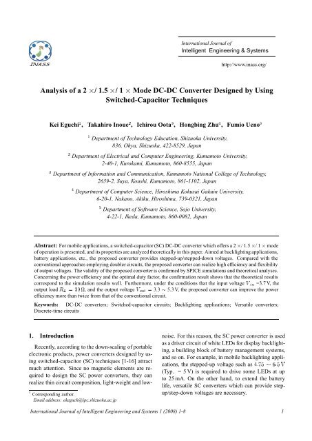
Power efficiency (%)10095908580757065~Theoretical (Doubler & Step down)Simulated (1.5 x mode)Simulated (2 x mode)Simulated (1 x mode)Theoretical (1.5 x mode)Theoretical (2 x mode)Theoretical (1 x mode)00.2 0.3 0.4 0.5 0.6 0.7 0.8Duty FactorRL = 30 ΩFigure 6. Power efficiency as function of parameter .Power efficiency (%)1009080Theoretical (Doubler & Step down)70605040Simulated (1.5 x mode)Simulated (2 x mode)30Simulated (1 x mode)20Theoretical (1.5 x mode)Theoretical (2 x mode)10Theoretical (1 x mode)00 10 20 30 40 50 60 70 80 90 100Output load (Ω)Figure 8. Power efficiency as function of output load Ê Ä .Vout (V)765432 x mode1.5 x mode1 x mode2Theoretical (1.5 x mode)1Theoretical (2 x mode)Theoretical (1 x mode) RL = 30 Ω00 10 20 30 40 50 60Time (μS)Figure 7. Output voltage with different conversion ratios.Power efficiency (%)1008060401 x mode(Proposed)1.5 x mode(Proposed)2 x mode(Proposed)20Proposed (2 x / 1.5 x / 1 x mode)Conventional (2 x / 1 x mode)01.5 2 2.5 3 3.5 4 4.5 5 5.5 6 6.5 7Output voltage (V)Figure 9. Power efficiency as function of output voltageÎ ÓÙØ .4. SimulationTo confirm the validity of the circuit design andthe theoretical analyses, SPICE simulations were performedunder the conditions that the input voltage Î Ò ¿Î, ½ ¾ ¿ ½ , Ì ½× and the onresistanceof the power-switch Ê ÓÒ ¼Å.Figure 6 shows the power efficiency of the proposedconverter as a function of the parameter . The theoreticalresults in Fig.6 were obtained by Eqs.(10),(13), (21), (24), (30), and (33), where Ê ÒØ Ê ÓÒ ¼Å and Ê Ä ¿¼ Å. In the case of 1.5 ¢, 2¢,and 1 ¢ mode, the converter can achieve the best efficiencyby setting the duty factor to 0.46, 0.55, and0.55, respectively. As Fig.6 shows, the results of thetheoretical analyses agree well with the simulated results.Figure 7 shows the output voltage Î ÓÙØ with differentconversion ratios. As Fig.7 shows, the proposedconverter can realize a 2 ¢/ 1.5 ¢/1¢ mode of operation,and the theoretical results and the simulated resultscorrespond well in the steady state. The theoreticalresults in Fig.7 were obtained by Eqs.(10), (12),(21), (23), (30), and (32), where Ê ÒØ Ê ÓÒ ¼Åand Ê Ä ¿¼Å.Figure 8 shows the power efficiency of the proposedconverter as a function of the output load Ê Ä . In thecase of the 1.5 ¢ mode, the power efficiency is 92.8% in the output current about ¾¼ Ñ. Of course,the power efficiency of the proposed converter canbe improved by using the power-switches with smallon-resistance. As Fig.8 shows, the theoretical resultsobtained by Eqs.(10), (13), (21), (24), (30), and (33)agree well with the simulated results.Figure 9 shows the comparison of the power efficiencybetween the proposed converter and the conventionalconverter as a function of the output voltageÎ ÓÙØ . In Fig.9, the regulation of the output voltagewas achieved by using an on-resistance controlscheme [9,12,13,16]. As Fig.9 shows, the proposedconverter can improve the power efficiency in the rangeof the 1.5 ¢ mode.5. ConclusionFor mobile applications, an SC DC-DC converterwhich offers a 2 ¢/ 1.5 ¢/ 1¢ mode of operationhas been proposed in this paper. The validity of thecircuit design was confirmed by theoretical analysesInternational Journal of Intelligent Engineering and Systems 1 (<strong>2008</strong>) 1-8 6
and SPICE simulations.Concerning the power efficiency and the optimalduty factor, the derived theoretical formulas will behelpful to estimate the circuit characteristics, becausethe theoretical results and the simulation results correspondedwell. Furthermore, the SPICE simulationsshowed that the proposed converter can realize a 2¢/ 1.5 ¢/ 1¢ mode of operation. Under the conditionsthat the input voltage Î Ò =3.7 V, the outputload Ê Ä ¿¼Å, and the output voltage Î ÓÙØ 3.3 5.3 V, the proposed converter can improve the powerefficiency more than twice from that of the conventionalcircuit.The further improvement of efficiency is left to thefuture study.AcknowledgementsThis work is supported by the Ministry of Education,Culture, Sports, Science and Technology, Grant-in-Aid for Scientific Research (B), 18360184, 2007. Andthe CAD tools used in this work is supported by VLSIDesign and Education Center (VDEC), the Universityof Tokyo in collaboration with On- Semiconductor,Nippon Motorola LTD., HOYA Corporation, and KY-OCERA Corporation.References[1] I.Harada, F.Ueno, T.Inoue, and I.Oota, ”Characteristicsanalysis of Fibonacci type SC transformer,”T.IEICE, Fundamentals, Vol.E75-A, No.6, pp.655-662, 1992.[2] T.Tanzawa and T.Tanaka, ”A dynamic analysis of theDickson charge pump circuit,” T.IEEE, Solid-StateCircuits, Vol.32, No.8, pp.1237-1240, 1997.[3] N.Hara, I.Oota, F.Ueno, and T.Inoue, ”A new ringtype set-up switched-capacitor DC-DC converterwith low inrush current at start-up and low currentripple in steady state,” T. IEEJ, Vol.J81-CII, No.7,pp.600-612, 1998.[4] N.Hara, I.Oota, I.Harada, and F.Ueno, ”Programmablering type switched-capacitor DC-DCconverters,” T. IEEJ, Vol.J82-C-II, No.2, pp.56-68,1999.[5] S.H.Chung, ”Design and analysis of a switchedcapacitor-basedstep-up DC/DC converter with continuousinput current,” IEEE Trans. Circuits Systs.I,Vol.46, No.6, pp.722-730, 1999.[6] T.Myono, A.Uemoto, S.Kawai, E.Nishibe,S.Kikuchi, T.Iijima, and H.Kobayashi, ”Highefficiencycharge-pump circuits with large currentoutput for mobile equipment applications,” T.IEICE,Electron., Vol.E84-C, No.10, pp.1602-1611, 2001.[7] K.Min and J.Ahn, ”CMOS charge pumps usingcross-coupled charge transfer switches with improvedvoltage pumping gain and low gate-oxidestress for low-voltage memory circuits,” T. IEICE,Electron., Vol.E85-C, No.1, pp.225-229, 2002.[8] K.Yamada, N.Fujii, and S.Takagi, ”Capacitancevalue free switched capacitor DC-DC voltage converterrealizing arbitrary rational conversion ratio,”T. IEICE, Fundamentals, Vol.E87-A, No.2, pp.344-349, 2004.[9] K.Eguchi, F.Ueno, H.Zhu, T.Tabata, and T.Inoue,”Design of a charge-average type SC DC-DC converterfor cellular phone,” T. IEEJ, Vol.125-C, No.1,pp.37-42, 2005.[10] S.V.Cheong, S.H.Chung, and A.Ioinovici, ”Inductorlessdc-to-dc converter with high power density,”IEEE Trans. Ind. Electron., Vol.41, pp.208-215,1994.[11] O.C.Mak, Y.C.Wong, and A.Ioinovici, ”Step-up dcpower supply based on a switched-capacitor circuit,”IEEE Trans. Ind. Electron., Vol.42, pp.90-97, 1995.[12] F.Ueno, T.Inoue, T.Umeno, and I.Oota, ”Analysisand application of switched-capacitor transformersby formulation,” Electron. Commun. Japan Pt.II Electron., Vol.73, No.9, pp.91-103, 1990.[13] S.H.Chung, S.Y.Hui, and S.C.Tang, ”Developmentof a multistage current-controlled switched-capacitorstep-down DC/DC converter with continuous inputcurrent,” IEEE Trans. Circuits Systs.I, Vol.47, No.7,pp.1017-1025, 2000.[14] P.Favrat, P.Deval, M.J.Declercq, ”A high-efficiencyCMOS voltage doubler,” IEEE journal of Solid-StateCircuits, Vol.33, No.3, pp.410-416, 1998.[15] D.Maksimovic, S.Dhar, ”Switched-capacitor DC-DC converters for low-power on-chip applications,”Proc. of IEEE PESC’1999, Vol.1, pp.54-59, 1999.[16] B.R.Gregoire, ”A compact switched-capacitor regulatedcharge pump power supply,” IEEE J.Solid-StateCircuits, Vol.41, No.8, pp.1944-1953, 2006.6. AppendixIn this section, the properties of the voltage doublercircuit are analyzed.Figure 10 shows the conventional converter 4 proposedin [14,16]. In Fig.10, the switches Ë ½ and Ë ¾are driven by non-overlapped 2-phase clock pulses.Figure 11 shows the instantaneous equivalent circuitsof the converter. In the case of ËØØ Ì ½, thecapacitor ½ is charged by the input voltage Î Ò viaË ½ ’s. Therefore, the voltage of ½ becomes Î Ò . Inthis timing, the output voltage is provided by ¾ .On The SC voltage converter LM2681 produced by National SemiconductorCorporation has the same structure.International Journal of Intelligent Engineering and Systems 1 (<strong>2008</strong>) 1-8 7
In Eq.(41), the optimal duty factor is ¼. FromEqs.(38) and (41), the equivalent circuit of the conventionalconverter is expressed by the following de-Therefore, the following equation is derived:¡ÕÌ ½ ½ ÌVinS1VoutS2C 1 C 2 (37) S2 S1Figure 10. Conventional converter.Δq Τ1,VinRonVoutΔq Τ1,VoutwhereVinC 1 C 2Ï Ì ½ ¾Ê ÓÒÌ ½ ´¡Õ½ Ì ½ µ¾RonΔq Τ2,VinRonΔq Τ2,VoutVoutVinRonC 1 C 2Ï ¾Ê ÓÒÌ ½ Ì ´¡Õ Î ÓÙص ¾Ê Ë Ì ¾, the inputterminant: ÎÒÁ Ò¡ÕÌ ½ ·¡Õ Ì ¾ ¾ ¼ ½ Ê Ë ¼ (34)½¼ ¼ ½¾ÎÓÙØÁ ÓÙØ¡Õ Ì ½ÎÒ ¡ÕÌ ½ ¾½Ê Ä Á ÓÙØÒ ¡Õ Ì ½ÎÓÙØ ¡ÕÌ ¾ ½ (35) ¾ ¾Ê Ä Á ÓÙØ · ÊË Á ÓÙØ¡Õ Ì ¾ÎÒ ¡ÕÌ ½ ¾Ò ¡Õ Ì ¾ÎÓÙØ ¡ÕÌ ½ ¾ ·¡Õ¾ Ì ¾ (36)Á Ò ´¡Õ Ì ½ÎÒ ·¡Õ Ì ¾ÎÒ µÌ ¾¡ÕÌ ½ ½Ì(a) ËØØ Ì ½ (Ë ½ ÇÒ and Ë ¾ Ç)(b) ËØØ Ì ¾ (Ë ½ Ç and Ë ¾ ÇÒ)Figure 11. Instantaneous equivalent circuits of Fig.10.the other hand, in the case of ËØØvoltage Î Ò and the capacitor ½ are connected in seriesvia Ë ¾ ’s. Therefore, a stepped-up voltage ¾Î Ò isobtained in the output terminal under no load condition.The properties of the conventional converter canbe obtained as follows:In the steady state, the differential values of theelectric charges in ½ ´ ½ ¾µ satisfyIn the case of ËØØ Ì ½, ¡Õ Ì ½ÎÒ and ¡Õ Ì ½ÎÓÙØ aregiven byOn the other hand, in the case of ËØØ Ì ¾, ¡Õ Ì ¾ÎÒand ¡Õ Ì ¾ÎÓÙØ are given byFrom Eqs.(34) (36), the average currents of the inputand the output are given byÒ Á ÓÙØ ´¡Õ Ì ½ÎÓÙØ ·¡Õ Ì ¾ÎÓÙØ µÌÁ Ò ¾Á ÓÙØ (38)In Fig.11, the energy consumed by resistors in oneperiod, Ï Ì , can be expressed byÏ Ì Ï Ì ½ · Ï Ì ¾ (39)Ò Ï ¾Ê ÓÒÌ ¾ Ì ¾ ´¡Õ½ Ì ¾ µ¾ From Eqs.(34) (37), Eq.(39) can be rewritten asÒ Ï Ì ¾ ¾Ê ÓÒ´½ µÌ ´¡Õ Î ÓÙص ¾ (40)By substituting Eq.(40) into Eq.(39), the SC resistanceof the doubler circuit, Ê Ë , can be obtained by¾´½ µ ¡ Ê ÓÒ (41) (42)From Eq.(42), the power efficiency of the conventionalconverter can be given byÊ ÄÊ Ä · Ê Ë (43)From Eqs.(25) and (41), in the case of the 2 ¢ mode,the SC resistance of the proposed converter is largerthan that of the conventional converter. However, thedifference between Eqs.(25) and (41) is only Ê ÒØ .As Fig.9 shows, the difference between the proposedconverter and the conventional converter in the efficiencyof the 2 ¢ mode is very small. Furthermore, inthe conventional converter, the power efficiency decreasesstrongly by the regulation, because the conventionalconverter cannot achieve a 1.5 ¢ mode ofoperation.International Journal of Intelligent Engineering and Systems 1 (<strong>2008</strong>) 1-8 8