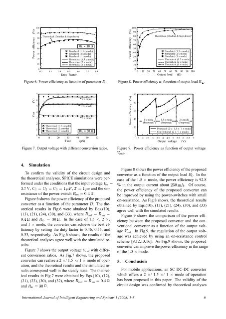
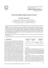
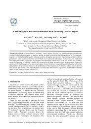
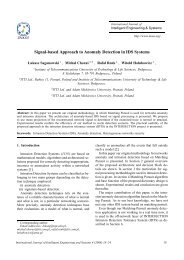
Power efficiency (%)10095908580757065~Theoretical (Doubler & Step down)Simulated (1.5 x mode)Simulated (2 x mode)Simulated (1 x mode)Theoretical (1.5 x mode)Theoretical (2 x mode)Theoretical (1 x mode)00.2 0.3 0.4 0.5 0.6 0.7 0.8Duty FactorRL = 30 ΩFigure 6. Power efficiency as function of parameter .Power efficiency (%)1009080Theoretical (Doubler & Step down)70605040Simulated (1.5 x mode)Simulated (2 x mode)30Simulated (1 x mode)20Theoretical (1.5 x mode)Theoretical (2 x mode)10Theoretical (1 x mode)00 10 20 30 40 50 60 70 80 90 100Output load (Ω)Figure 8. Power efficiency as function of output load Ê Ä .Vout (V)765432 x mode1.5 x mode1 x mode2Theoretical (1.5 x mode)1Theoretical (2 x mode)Theoretical (1 x mode) RL = 30 Ω00 10 20 30 40 50 60Time (μS)Figure 7. Output voltage with different conversion ratios.Power efficiency (%)1008060401 x mode(Proposed)1.5 x mode(Proposed)2 x mode(Proposed)20Proposed (2 x / 1.5 x / 1 x mode)Conventional (2 x / 1 x mode)01.5 2 2.5 3 3.5 4 4.5 5 5.5 6 6.5 7Output voltage (V)Figure 9. Power efficiency as function of output voltageÎ ÓÙØ .4. SimulationTo confirm the validity of the circuit design andthe theoretical analyses, SPICE simulations were performedunder the conditions that the input voltage Î Ò ¿Î, ½ ¾ ¿ ½ , Ì ½× and the onresistanceof the power-switch Ê ÓÒ ¼Å.Figure 6 shows the power efficiency of the proposedconverter as a function of the parameter . The theoreticalresults in Fig.6 were obtained by Eqs.(10),(13), (21), (24), (30), and (33), where Ê ÒØ Ê ÓÒ ¼Å and Ê Ä ¿¼ Å. In the case of 1.5 ¢, 2¢,and 1 ¢ mode, the converter can achieve the best efficiencyby setting the duty factor to 0.46, 0.55, and0.55, respectively. As Fig.6 shows, the results of thetheoretical analyses agree well with the simulated results.Figure 7 shows the output voltage Î ÓÙØ with differentconversion ratios. As Fig.7 shows, the proposedconverter can realize a 2 ¢/ 1.5 ¢/1¢ mode of operation,and the theoretical results and the simulated resultscorrespond well in the steady state. The theoreticalresults in Fig.7 were obtained by Eqs.(10), (12),(21), (23), (30), and (32), where Ê ÒØ Ê ÓÒ ¼Åand Ê Ä ¿¼Å.Figure 8 shows the power efficiency of the proposedconverter as a function of the output load Ê Ä . In thecase of the 1.5 ¢ mode, the power efficiency is 92.8% in the output current about ¾¼ Ñ. Of course,the power efficiency of the proposed converter canbe improved by using the power-switches with smallon-resistance. As Fig.8 shows, the theoretical resultsobtained by Eqs.(10), (13), (21), (24), (30), and (33)agree well with the simulated results.Figure 9 shows the comparison of the power efficiencybetween the proposed converter and the conventionalconverter as a function of the output voltageÎ ÓÙØ . In Fig.9, the regulation of the output voltagewas achieved by using an on-resistance controlscheme [9,12,13,16]. As Fig.9 shows, the proposedconverter can improve the power efficiency in the rangeof the 1.5 ¢ mode.5. ConclusionFor mobile applications, an SC DC-DC converterwhich offers a 2 ¢/ 1.5 ¢/ 1¢ mode of operationhas been proposed in this paper. The validity of thecircuit design was confirmed by theoretical analysesInternational Journal of Intelligent Engineering and Systems 1 (<strong>2008</strong>) 1-8 6
and SPICE simulations.Concerning the power efficiency and the optimalduty factor, the derived theoretical formulas will behelpful to estimate the circuit characteristics, becausethe theoretical results and the simulation results correspondedwell. Furthermore, the SPICE simulationsshowed that the proposed converter can realize a 2¢/ 1.5 ¢/ 1¢ mode of operation. Under the conditionsthat the input voltage Î Ò =3.7 V, the outputload Ê Ä ¿¼Å, and the output voltage Î ÓÙØ 3.3 5.3 V, the proposed converter can improve the powerefficiency more than twice from that of the conventionalcircuit.The further improvement of efficiency is left to thefuture study.AcknowledgementsThis work is supported by the Ministry of Education,Culture, Sports, Science and Technology, Grant-in-Aid for Scientific Research (B), 18360184, 2007. Andthe CAD tools used in this work is supported by VLSIDesign and Education Center (VDEC), the Universityof Tokyo in collaboration with On- Semiconductor,Nippon Motorola LTD., HOYA Corporation, and KY-OCERA Corporation.References[1] I.Harada, F.Ueno, T.Inoue, and I.Oota, ”Characteristicsanalysis of Fibonacci type SC transformer,”T.IEICE, Fundamentals, Vol.E75-A, No.6, pp.655-662, 1992.[2] T.Tanzawa and T.Tanaka, ”A dynamic analysis of theDickson charge pump circuit,” T.IEEE, Solid-StateCircuits, Vol.32, No.8, pp.1237-1240, 1997.[3] N.Hara, I.Oota, F.Ueno, and T.Inoue, ”A new ringtype set-up switched-capacitor DC-DC converterwith low inrush current at start-up and low currentripple in steady state,” T. IEEJ, Vol.J81-CII, No.7,pp.600-612, 1998.[4] N.Hara, I.Oota, I.Harada, and F.Ueno, ”Programmablering type switched-capacitor DC-DCconverters,” T. IEEJ, Vol.J82-C-II, No.2, pp.56-68,1999.[5] S.H.Chung, ”Design and analysis of a switchedcapacitor-basedstep-up DC/DC converter with continuousinput current,” IEEE Trans. Circuits Systs.I,Vol.46, No.6, pp.722-730, 1999.[6] T.Myono, A.Uemoto, S.Kawai, E.Nishibe,S.Kikuchi, T.Iijima, and H.Kobayashi, ”Highefficiencycharge-pump circuits with large currentoutput for mobile equipment applications,” T.IEICE,Electron., Vol.E84-C, No.10, pp.1602-1611, 2001.[7] K.Min and J.Ahn, ”CMOS charge pumps usingcross-coupled charge transfer switches with improvedvoltage pumping gain and low gate-oxidestress for low-voltage memory circuits,” T. IEICE,Electron., Vol.E85-C, No.1, pp.225-229, 2002.[8] K.Yamada, N.Fujii, and S.Takagi, ”Capacitancevalue free switched capacitor DC-DC voltage converterrealizing arbitrary rational conversion ratio,”T. IEICE, Fundamentals, Vol.E87-A, No.2, pp.344-349, 2004.[9] K.Eguchi, F.Ueno, H.Zhu, T.Tabata, and T.Inoue,”Design of a charge-average type SC DC-DC converterfor cellular phone,” T. IEEJ, Vol.125-C, No.1,pp.37-42, 2005.[10] S.V.Cheong, S.H.Chung, and A.Ioinovici, ”Inductorlessdc-to-dc converter with high power density,”IEEE Trans. Ind. Electron., Vol.41, pp.208-215,1994.[11] O.C.Mak, Y.C.Wong, and A.Ioinovici, ”Step-up dcpower supply based on a switched-capacitor circuit,”IEEE Trans. Ind. Electron., Vol.42, pp.90-97, 1995.[12] F.Ueno, T.Inoue, T.Umeno, and I.Oota, ”Analysisand application of switched-capacitor transformersby formulation,” Electron. Commun. Japan Pt.II Electron., Vol.73, No.9, pp.91-103, 1990.[13] S.H.Chung, S.Y.Hui, and S.C.Tang, ”Developmentof a multistage current-controlled switched-capacitorstep-down DC/DC converter with continuous inputcurrent,” IEEE Trans. Circuits Systs.I, Vol.47, No.7,pp.1017-1025, 2000.[14] P.Favrat, P.Deval, M.J.Declercq, ”A high-efficiencyCMOS voltage doubler,” IEEE journal of Solid-StateCircuits, Vol.33, No.3, pp.410-416, 1998.[15] D.Maksimovic, S.Dhar, ”Switched-capacitor DC-DC converters for low-power on-chip applications,”Proc. of IEEE PESC’1999, Vol.1, pp.54-59, 1999.[16] B.R.Gregoire, ”A compact switched-capacitor regulatedcharge pump power supply,” IEEE J.Solid-StateCircuits, Vol.41, No.8, pp.1944-1953, 2006.6. AppendixIn this section, the properties of the voltage doublercircuit are analyzed.Figure 10 shows the conventional converter 4 proposedin [14,16]. In Fig.10, the switches Ë ½ and Ë ¾are driven by non-overlapped 2-phase clock pulses.Figure 11 shows the instantaneous equivalent circuitsof the converter. In the case of ËØØ Ì ½, thecapacitor ½ is charged by the input voltage Î Ò viaË ½ ’s. Therefore, the voltage of ½ becomes Î Ò . Inthis timing, the output voltage is provided by ¾ .On The SC voltage converter LM2681 produced by National SemiconductorCorporation has the same structure.International Journal of Intelligent Engineering and Systems 1 (<strong>2008</strong>) 1-8 7