
You also want an ePaper? Increase the reach of your titles
YUMPU automatically turns print PDFs into web optimized ePapers that Google loves.
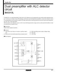
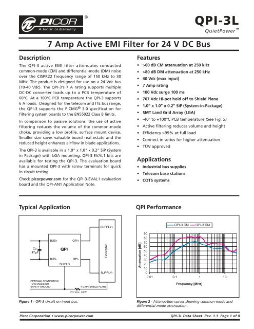
®<strong>QPI</strong>-3LQuietPower 7 Amp Active EMI Filter for 24 V DC BusDescriptionThe <strong>QPI</strong>-3 active EMI filter attenuates conductedcommon-mode (CM) and differential-mode (DM) noiseover the CISPR22 frequency range of 150 kHz to 30MHz. The product is designed for use on a 24 Vdc bus(10-40 Vdc). The <strong>QPI</strong>-3’s 7 A rating supports multipleDC-DC converter loads up to a PCB temperature of60°C. At a 100°C PCB temperature the <strong>QPI</strong>-3 supports6 A loads. Designed for the telecom and ITE bus range,the <strong>QPI</strong>-3 supports the PICMG ® 3.0 specification forfiltering system boards to the EN55022 Class B limits.In comparison to passive solutions, the use of activefiltering reduces the volume of the common-modechoke, providing a low profile, surface mount device.Smaller size saves valuable board real estate and thereduced height enhances airflow in blade applications.The <strong>QPI</strong>-3 is available in a 1.0" x 1.0" x 0.2" SiP (Systemin Package) with LGA mounting. <strong>QPI</strong>-3-EVAL1 kits areavailable for testing the <strong>QPI</strong>-3. The evaluation boardhas a mounted <strong>QPI</strong>-3 with screw terminals for quickin-circuit testing.Check picorpower.com for the <strong>QPI</strong>-3-EVAL1 evaluationboard and the <strong>QPI</strong>-AN1 Application Note.Features• >60 dB CM attenuation at 250 kHz• >80 dB DM attenuation at 250 kHz• 40 Vdc (max input)• 7 Amp rating• 100 Vdc surge 100 ms• 707 Vdc Hi-pot hold off to Shield Plane• 1.0” x 1.0” x 0.2” SiP (System-in-Package)• SMT Land Grid Array (LGA)• -40° to +100°C PCB temperature (See Fig. 5)• Active filtering reduces volume and height• Efficiency >99% at full load• Connect in series for higher attenuation• TÜV approvedApplications• Industrial bus supplies• Telecom base stations• COTS systemsTypical Application<strong>QPI</strong> PerformanceQ<strong>QPI</strong>-3 CM<strong>QPI</strong>-3 DMAttenuation [dB]90807060504030201000.01 0.1 1 10Frequency [MHz]RY=10 Ω, 1/4 WFigure 1 - <strong>QPI</strong>-3 circuit on input bus.Figure 2 - Attenuation curves showing common-mode anddifferential-mode attenuation.<strong>Picor</strong> Corporation • www.picorpower.com <strong>QPI</strong>-3L Data Sheet Rev. 1.1 Page 1 of 8
Absolute Maximum Ratings – Exceeding these parameters may result in permanent damage to the product.Pins Parameter Notes Min Max UnitsBUS+ to BUS- Input voltage Continuous -40 40 VdcBUS+ to BUS- Input voltage 100ms transient -100 100 VdcBUS+/BUS- to Shield Plane BUS inputs to Shield Hipot Per test std. +/-1500 Vdc<strong>QPI</strong>+ to <strong>QPI</strong>- Input to output current Continuous @ 25°C 7 AdcPackage Power dissipation VBUS = 48 V, IBUS = 7 Adc, 25°C 2.0 WPackage Operating temperature PCB to <strong>QPI</strong> Interface -40 100 °CPackage Thermal resistance Free air 50 °C/WPackage Junction temperature Internal @ Pdmax and 15°C/W 130 °CPackage Thermal resistance PCB layout (see Figs. 9 & 10) 1 15 °C/WPackage Storage temperature -40 125 °CPackage Re-flow temperature 20 second exposure @ 212 °CAll Pins ESD HBM +/-2 kVNote 1 - Refer to Figures 9 & 10 for PCB layout guidelines to achieve this thermal resistance when re-flowed onto the PCB.Electrical Characteristics – Parameter limits apply over the operating temp. range unless otherwise noted.Parameter Notes Min Typ Max UnitsBUS+ to BUS- input range Measured at 7 A 2 10 40 VdcBUS+ to <strong>QPI</strong>+ voltage drop Measured at 7 A 2 100 mVdcBUS- to <strong>QPI</strong>- voltage drop Measured at 7 A 2 20 mVdcCommon-mode insertion loss VBUS = 28 V frequency = 500 kHz 63 dBDifferential-mode insertion loss VBUS = 28 V frequency = 500 kHz 80 dBInput bias current at 40 Volts Input current from BUS+ to BUS- 8 mANote 2 - Refer to Figure 5 for current derating curve.THERM 1THERM 2<strong>QPI</strong>-3: (bottom view)<strong>QPI</strong>+SHIELD8765BUS-9 10 11 124 3 2 1<strong>QPI</strong>-13141516BUS+BUS+ 12,13,14BUS- 1,15,16<strong>QPI</strong>+ 7,8,9<strong>QPI</strong>- 2,3,4SHIELD 5,6THERM 1 10THERM 2 11Pad DesignationsPad DescriptionBUS-BUS+Negative bus potentialPositive bus voltageTHERM1THERM2Internal connection must be electricallyfloating but maximize copper landingfor heat sinking.<strong>QPI</strong>-<strong>QPI</strong>+Negative input to the converterPositive input to the converterShieldThe shield connects to the convertershield and Y capacitor common pointthrough RY.<strong>Picor</strong> Corporation • www.picorpower.com <strong>QPI</strong>-3L Data Sheet Rev. 1.1 Page 2 of 8
Applications InformationThe <strong>QPI</strong>-3 is an active EMI filter providing conductedcommon-mode and differential-mode attenuationfrom 150 kHz to 30 MHz. The <strong>QPI</strong>-3 attenuates noise atall frequencies covered by EN55022. Designers shouldbe aware that to select and qualify an EMI filter theymust test the filter in their equipment under the set upand conditions specified in the EMI standards that theyare trying to meet.Filter performance is highly dependent on severalfactors and cannot be derived from the attenuationcurves shown in Figure 2 alone. Performance is acomplex function of filter element impedances andnoise source impedances, which vary in magnitude andphase over the frequency spectrum. Measurementsshould be made in consultation with in-housecompliance testing or an independent EMI test facility.Figure 4 – Conducted EMI profile of a DC-DC Converterwith <strong>QPI</strong>-3.Test ExampleFigures 3 and 4 show the before and after plots of aDC-DC converter noise profile to demonstrate theperformance of the <strong>QPI</strong>-3. The plots were taken usingthe standard measurement technique and set up definedin CISPR22. The results show the total noise spectrumfor a standard DC-DC converter under load comparedto the EN55022 Class B Quasi-peak detection limit.Figure 3 – Conducted EMI profile of a DC-DC Converterwithout filter.The resulting plot in Figure 4 shows the <strong>QPI</strong>-3 iseffective in reducing the total conducted noisespectrum measured pre-filter to well below theEN55022 Class B Quasi-peak detection limit.Layout and CircuitApplication of the <strong>QPI</strong>-3 requires PCB layout practicessimilar to those used with passive EMI filters. The circuitin Figure 6 and the PCB layout in Figures 9 & 10 shouldbe used as a design guide to ensure successfulapplication of the <strong>QPI</strong>-3. Refer to the application note<strong>QPI</strong>- AN1 for additional PCB layout recommendations.Note: For optimum performance of the <strong>QPI</strong>-3 it iscritical to connect the <strong>QPI</strong>-3 Shield Plane (pins 5 & 6) tothe converter EMI Shield Plane (common point of C1-C4"Y" capacitors) thru RY as shown in Figure 6. If thesafety earth-ground connection (chassis or case) isconnected in the power conversion section of the PCBit should be at the input bus of the <strong>QPI</strong>-3 Shield Plane,shown as the optional connection in Figure 6.Connecting the converter EMI shield plane directly tochassis ground may degrade the <strong>QPI</strong>-3 attenuationperformance. The typical value for RY is 10 Ohms. Therecommended part is a 5% tolerance SMT1206 orsimilarly rated 0.25 W through-hole resister.<strong>QPI</strong>s will filter multiple DC-DC converters up to themaximum current rating. The schematic in Figure 7shows the required circuit for multiple DC-DCconverters. The Shield Plane should be added undereach converter as a common EMI Shield. Note that onlya single RY is required in a multiple converterconfiguration.<strong>Picor</strong> Corporation • www.picorpower.com <strong>QPI</strong>-3L Data Sheet Rev. 1.1 Page 3 of 8
PCB plane under converterBUS+<strong>QPI</strong>+VIN+VOUT+BUSSUPPLYCB47µF<strong>QPI</strong>CIN1CONVERTEROptional ConnectionBUS-SHIELDVIN- VOUT-C2 C3 C4SHIELD<strong>QPI</strong>-RY10 Ω, 1/4 WC1PCB plane under converterVIN+VOUT+CIN2CONVERTERVIN-VOUT-C5C6 C7 C8SHIELDAdditional ConvertersFigure 7 – Schematic for supporting multiple DC-DC converters. Note only a single RY is required. Use values recommended by convertermanufacturer for CIN and Y-capacitors C1-C8.PCB plane under converterBUS+<strong>QPI</strong>+BUS+<strong>QPI</strong>+VIN+VOUT+BUSSUPPLYCB47 µF<strong>QPI</strong><strong>QPI</strong>CINCONVERTEROptional ConnectionBUS-SHIELDVIN- VOUT-C2 C3 C4SHIELD<strong>QPI</strong>-BUS-SHIELDRYC1<strong>QPI</strong>-10 Ω, 1/4 WFigure 8 – Series connection of <strong>QPI</strong> for higher attenuation.<strong>Picor</strong> Corporation • www.picorpower.com <strong>QPI</strong>-3L Data Sheet Rev. 1.1 Page 5 of 8
0.17730.984345.000°13 places0.06250.08200.0820R0.04100.4920.4410.4000.3000.1000.0000.1000.8000<strong>QPI</strong> SIP Package(Bottom View)0.98432 places0.12500.08200.3000.4000.4410.4920.02000.4920.4410.3000.1000.0000.1000.3000.4410.492Figure 11 – <strong>QPI</strong> package dimensions and pad locations.0.48500.44100.39700.30000.10000.00000.1000<strong>QPI</strong> Package Outline<strong>QPI</strong> PCB Pad Pattern(Top View)0.49213 places2 places0.0880R0.04400.04400.0440THERM 2 THERM 10.050 0.050BUS+<strong>QPI</strong>+0.4410 0.44100.0500.0500.30000.39700.48500.06550.0880BUS-SHIELD0.0500.48500.44100.39700.30000.10000.00000.10000.30000.39700.44100.48500.1310<strong>QPI</strong>-0.050Figure 12 –Recommended PCB layout pattern. Use 1.3mm clearance around shield pads 5 & 6 to adjacent lands. See Figures 9 & 10 forrecommended connection layouts.<strong>Picor</strong> Corporation • www.picorpower.com <strong>QPI</strong>-3L Data Sheet Rev. 1.1 Page 7 of 8
<strong>Vicor</strong>’s comprehensive line of power solutions includes high-density AC-DC & DC-DC modulesand accessory components, fully configurable AC-DC & DC-DC power supplies, and completecustom power systems.Information furnished by <strong>Vicor</strong> is believed to be accurate and reliable. However, no responsibility isassumed by <strong>Vicor</strong> for its use. No license is granted by implication or otherwise under any patent or patentrights of <strong>Vicor</strong>. <strong>Vicor</strong> components are not designed to be used in applications, such as life supportsystems, wherein a failure or malfunction could result in injury or death. All sales are subject to <strong>Vicor</strong>’sTerms and Conditions of Sale, which are available upon request.Specifications are subject to change without notice.<strong>Vicor</strong> Corporation25 Frontage Road, Andover, MA, USA 01810Tel: 800-735-6200 Fax: 978-475-6715Email<strong>Vicor</strong> Express: vicorexp@vicr.comTechnical Support: apps@vicr.com<strong>Picor</strong> Corporation • www.picorpower.com • <strong>QPI</strong>-3L Data Sheet P/N 28956 Rev. 1.1 10/04/10M