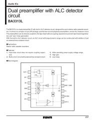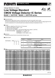
datasheet - SE Spezial-Electronic AG
datasheet - SE Spezial-Electronic AG
datasheet - SE Spezial-Electronic AG
- No tags were found...

You also want an ePaper? Increase the reach of your titles
YUMPU automatically turns print PDFs into web optimized ePapers that Google loves.
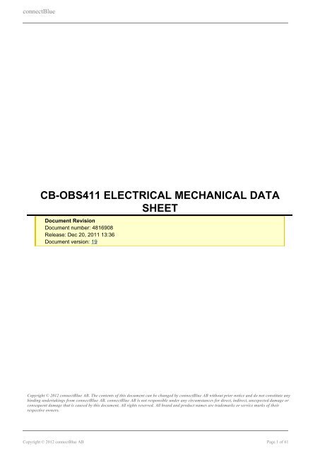
connectBlueCB-OBS411 ELECTRICAL MECHANICAL DATASHEETDocument RevisionDocument number: 4816908Release: Dec 20, 2011 13:36Document version: 19Copyright © 2012 connectBlue AB. The contents of this document can be changed by connectBlue AB without prior notice and do not constitute anybinding undertakings from connectBlue AB. connectBlue AB is not responsible under any circumstances for direct, indirect, unexpected damage orconsequent damage that is caused by this document. All rights reserved. All brand and product names are trademarks or service marks of theirrespective owners.Copyright © 2012 connectBlue AB Page 1 of 61
connectBlue1 Table of Content1 Table of Content2 Introduction2.1 Related Documents2.2 Product Variants2.3 Block Diagram3 Electrical Interface and Connectors3.1 Pin Numbering3.2 Pin Description3.3 Characteristics3.4 Hardware Reset4 Operating Status5 Antennas5.1 Surface Mounted Antennas (Internal)5.2 External antennas6 Mechanics6.1 Module Outlines6.2 Using the J2/J3 Board-to-Board Connectors6.3 Using Press-Fit Nuts for Mounting the Module6.4 Using the J6 PCB solder pads6.5 Antenna Issues7 Bluetooth Information7.1 General information7.2 Bluetooth Qualification information8 Regulatory Information8.1 Declaration of Conformity8.2 Safety Compliance8.3 FCC and IC Compliance8.4 UL listing information8.5 Japan Radio Equipment Compliance (TELEC)8.6 Compliance with RoHS directive9 Guidelines for Efficient and Safe Use9.1 General9.2 Product Care9.3 Radio Frequency Exposure9.4 <strong>Electronic</strong> Equipment9.5 Potentially Explosive Atmospheres9.6 Power Supply10 Application Notes10.1 Step-by-Step Guide10.2 Design ExamplesCopyright © 2012 connectBlue AB Page 2 of 61
connectBlue2 IntroductionThe hardware of the cB-OBS411 products are refered as cB-0925 and the module is Type Approved with thetype name cB-0925.cB-OBS411 is a small size Bluetooth module based on the ST-Ericsson STLC2500 radio chip and a STMicroelectronics STM32F10x microprocessor. The module is available in different configuration (see ProductVariants) with internal antennas or a U.FL. connector for connecting an external antenna.Figure 1: cB-OBS411i-04 OEM Serial Port Adapter with internal antenna2.1 Related DocumentsThere are some documents related to the Serial Port Adapter:The Bluetooth Serial Port Adapter AT Commands document contains a description of the ATcommands supported in the Serial Port Adapter. It also contains information on how to use the ATcommands to create Bluetooth applications.The cB-OBS411 Electrical & Mechanical Datasheet (this document) contains important informationabout the OEM Serial Port Adapter. Read this document if you are using the OEM Serial Port Adapter.The Bluetooth Qualification Guide contains a step by step guide that describes how to create aBluetooth end product listing for products integrating the cB-OBS411.The Bluetooth Serial Port Adapter Compatibility iPhone and Android document.Copyright © 2012 connectBlue AB Page 3 of 61
connectBlue2.2 Product VariantsThe module is available in three antenna options. Please note that the j-version (extra low antenna profile) isavailable on special request only, since the antenna performance may be limited because of the small size ofthe antenna.Table 1: Product variantsProduct NameRegulatory IDFCC IDIC IDMIC IDBluetoothTypeDescriptioncB-OBS411i-04cB-0925PVH09255325A-0925204WW11100300Class 1Outputpower: 5dBmEIRP*Sensitivity:-85 dBmEIRP*OEM Serial PortAdapter 411 withinternal antenna,board-to-board andsolder pads.cB-OBS411i-06***cB-0925PVH09255325A-0925204WW11100300Class 1Outputpower: 5dBmEIRP*Sensitivity:-85 dBmEIRP*OEM Serial PortAdapter 411 withinternal antenna,JST wire connector,board-to-board andsolder pads.cB-OBS411j-04cB-0925PVH09255325A-0925204WW11100300Class 1Outputpower: 4dBmEIRP*Sensitivity:-84 dBmEIRP*OEM Serial PortAdapter 411 withinternal antenna(extra low antennaprofile),board-to-board andsolder pads.Available on specialrequest only.cB-OBS411j-06***cB-0925PVH09255325A-0925204WW11100300Class 1Outputpower: 4dBmEIRP*Sensitivity:-84 dBmEIRP*OEM Serial PortAdapter 411 withinternal antenna(extra low antennaprofile) with internalantenna, JST wireconnector,board-to-board andsolder pads.Available on specialrequest only.Copyright © 2012 connectBlue AB Page 4 of 61
connectBluecB-OBS411x-04cB-0925PVH09255325A-0925204WW11100300Class 1Outputpower: 4to 6 dBmEIRP**Sensitivity:-84 to -86dBmEIRP**OEM Serial PortAdapter 411 withU.FL. connector forexternal antenna,board-to-board andsolder pads.cB-OBS411x-06***cB-0925PVH09255325A-0925204WW11100300Class 1Outputpower: 4to 6 dBmEIRP**Sensitivity:-84 to -86dBmEIRP**OEM Serial PortAdapter 411 withU.FL. connector forexternal antenna,JST wire connector,board-to-board andsolder pads.* EIRP is including antenna gain.** EIRP is including antenna gain and cable loss and thus depends on the antenna selection.*** The JST connector is specified down to -25 ºC. See #Environmental for more information.2.3 Block DiagramFigure 2: Block diagram of cB-OBS411Copyright © 2012 connectBlue AB Page 5 of 61
connectBlue3 Electrical Interface and ConnectorsThis section describes the signals available on the module interface connectors. There are three ways toconnect to the OEM Serial Port Adapter:Via the PCB solder pads on the edge of the PCB, J6 (see Figure 3). See Section "#Using the J6 PCBsolder pads" for more information.Via the 2x20-pin 1mm pitch board-to-board (one piece part) connectors, J2 through J3. The J2 to J3connectors on the OEM Serial Port Adapter exist on the module only as a mating PCB-layout pattern(see Figure 3). See Section " Using the J2/J3 Board-to-Board Connectors" for more information.Optional: Via the JST connector, J8 (see Figure 4). The connector is a 6 poles wire connector. The pitchis 1mm. The manufacturer of the mounted connector is JST and the part number is SM06B-SRSS-TB.The SM06B-SRSS-TB connector is mated with the wire connector SHR-06V-S from JST. Otherconnector options are also available from JST.Figure 3: The solder pads J6 are available on the long edges of the bottom side of the PCB. Theboard-to-board connector pads J2-J3 are located between the mounting holes.Figure 4: The JST connector J8 is mounted on the component sida of the PCB as an option.Copyright © 2012 connectBlue AB Page 6 of 61
connectBlue3.1 Pin Numbering3.1.1 J2, J3 and J6 bottom side connectorsFigure 5: Bottom view of the PCB with the pin numbering of the J2, J3 and the J6 connectors.3.1.2 J8 JST connectorFigure 6: Top view of the PCB with the pin numbering of the J8 connector.Copyright © 2012 connectBlue AB Page 7 of 61
connectBlue3.2 Pin DescriptionTable 2: Signals description.J2PinNbrJ3PinNbrJ6PinNbrJ8PinNbrSignal NameSignalLevelTypeIOpinNbrDescription1-2 8, 12 3,25***1 VSS Ground - GND3-4 - 4 2 VCC_3V3 3.3 V In - 3.0 - 6.0 VDC powersupply5-10 5,15-1814-17,19-21,29- - - - - Reserved, do not connect.- 14 23 - - CMOS In/Out 10 AT command controlled IOpin. See the "BluetoothSerial Port Adapter ATCommands"documentation for moreinfo.- 13 24 - - CMOS In/Out 11 AT command controlled IOpin. See the "BluetoothSerial Port Adapter ATCommands"documentation for moreinfo.- 11 26 - - CMOS In/Out 12 AT command controlled IOpin. See the "BluetoothSerial Port Adapter ATCommands"documentation for moreinfo.- 7 27 - - CMOS In/Out 13 AT command controlled IOpin. See the "BluetoothSerial Port Adapter ATCommands"documentation for moreinfo.- 6 28 - - CMOS In/Out 14 AT command controlled IOpin. See the "BluetoothSerial Port Adapter ATCommands"documentation for moreinfo.Copyright © 2012 connectBlue AB Page 8 of 61
connectBlue- 1 31 - - CMOS In/Out 15 AT command controlled IOpin. See the "BluetoothSerial Port Adapter ATCommands"documentation for moreinfo.- 2 32 - - CMOS In/Out 16 AT command controlled IOpin. See the "BluetoothSerial Port Adapter ATCommands"documentation for moreinfo.- 3 33 - - CMOS In/Out 17 AT command controlled IOpin. See the "BluetoothSerial Port Adapter ATCommands"documentation for moreinfo.- 4 34 - - CMOS In/Out 18 AT command controlled IOpin. See the "BluetoothSerial Port Adapter ATCommands"documentation for moreinfo.11 - 7 - RED/Mode CMOS Out 2 RED:Logic Red LEDSignal (see the #OperatingStatus section). Activelow.Mode: Not used oncB-OBS411. This pin isalso used to select Logiclevel mode (instead ofRS232) for connectBlueproducts with internalRS232 driver. To becompatible with theseproducts check the<strong>datasheet</strong> for theseproducts about this signal.Copyright © 2012 connectBlue AB Page 9 of 61
connectBlue12 - 6 - Switch-0 CMOS In 1 Used for the "Connect onexternal signal" function,see the Serial PortAdapter AT commandSpecification for moreinformation on theFunction switch. Activelow.A secondary function isthat the module willrestore all factory settingsif both the Switch-1 andSwitch-0 signals are lowduring start up.See the Serial PortAdapter AT commandSpecification for moreinformation on theRestoring DefaultConfiguration functionality.See section Switch-0Signal for designexamples.Copyright © 2012 connectBlue AB Page 10 of 61
connectBlue13 - 8 - GREEN/Switch-1 CMOS In/Out 3 This signal is multiplexed:GREEN:Logic Green LEDSignal (see the #OperatingStatus section). Not validuntil 500ms after startup.Active low.Switch-1: If the level onthis pin is pulled-down**the unit goes back todefault serial settings. TheSwitch-1 input is onlyactive during the first500ms after startup. Themodule will restore allfactory settings if both theSwitch-1 and Switch-0signals are low during startup.See the Serial PortAdapter AT commandSpecification for moreinformation on theRestoring DefaultConfiguration functionality.See section GREEN/Switch-1 for design examples.14 - 9 - BLUE CMOS Out 4 Logic Blue LED Signal(see the #OperatingStatus section). Activelow.Note:Signal will flicker atdata transmission.See section #BLUE Signalfor design examples.15 - 10 5 UART-CTS* CMOS In 5 Clear To Send. Hardwareflow control. Active low.16 - 11 3 UART-TxD* CMOS Out 6 Transmit Data. "0" : Low,"1" : High17 - 12 6 UART-RTS* CMOS Out 7 Request To Send.Hardware flow control.Active low.18 - 13 4 UART-RxD* CMOS In 8 Receive Data. "0" : Low,"1" : HighCopyright © 2012 connectBlue AB Page 11 of 61
connectBlue19 - 5 - UART-DTR* CMOS Out 0 Data Terminal Ready.Active low.20 - 18,30***- 19 1,22***- UART-DSR* CMOS In 9 Data Set Ready. Activelow.- CMOS In Hardware reset- 9 36 - SerialSelect-0 /I²C-SDACMOS Out /Bidirectional20 SerialSelect-0: Controlsignal for external serialtransceivers.See Appendix SerialInterface section for moreinfo.I²C-SDA: I²C Serial data.Only used forcommunicating with anexternal Apple®AuthenticationCoprocessor, see the Bluetooth Serial PortAdapter CompatibilityiPhone and Android document for more info.- 10 35 - SerialSelect-1 /I²C-SCLCMOS Out 19 SerialSelect-1: Controlsignal for external serialtransceivers.See Appendix SerialInterface section for moreinfo.I²C-SCL: I²C clock. Onlyused for communicatingwith an external Apple®AuthenticationCoprocessor, see the Bluetooth Serial PortAdapter CompatibilityiPhone and Android document for more info.- 20 2 - VCC_2V85 2.85 V Out - Regulated interfacevoltage for voltage levelshifting, max 10mA.* All signals are logic level UART signals (typically 0 - 2.85VDC).** Use max 4.7kOhm as pull-down which is different to previous product generations from connectBlue.*** Alternative signal pin recommended to use in new designs (both signal pins should be connected).Copyright © 2012 connectBlue AB Page 12 of 61
connectBlue3.3 CharacteristicsThe cB-OBS411 module has linear power supplies, which means that the current is constant if the voltagesupply is changed.3.3.1 Power supplyNOTERead the Guidelines for Efficient and Safe Use before using the modules.Table 3: Power supplySymbol Parameter Value UnitVCC_3V3 Power supply (Unregulated*) Min 3.0 VDCMax 6.0 VDCThe module is equipped with internal linear voltage regulators.Table 4: Current consumptionSymbol Mode Value UnitI @ VCC_3V3 =CC3.3VNot connected Connectable, discoverable Average 14.5 mAPeak 64.5 mANot connected, stop modeenabledNot connectable, notdiscoverableAverage 0.6 mAPeak 0.6 mAConnectable, notdiscoverableAverage 0.8 mAPeak 37.2 mAConnectable, discoverable Average 1.2 mAPeak 37.2 mAConnected Idle or Receiving Average 15.5 mAPeak 57.8 mACopyright © 2012 connectBlue AB Page 13 of 61
connectBlueTransmitting @115.2kbit/s Average 25.1 mAPeak 64.9 mAInquiry Average 35.5 mAPeak 71.0 mA3.3.2 Input/Output signalsTable 5: Input/output signalsSymbol Parameter Value UnitV Low IN Logic LOW level input voltage Min -0.50 VMax 0.80 VV HighIN UART Logic HIGH level input voltage UART interface and RED signal Min 2.00 VMax 5.50 VV High IN Logic HIGH level input voltage all other IO pins Min 2.00 VMax 3.35 VV Low OUT Logic LOW level output voltage Max 0.40 VV High OUT Logic HIGH level output voltage Min 2.40 VI IO Sink and source current Max 4 mAC IO I/O pin capacitance Typ 5 pFR IN_PULL-UP Input signals (including ) internal pull-upMin 30 kOhmTyp 40 kOhmMax 50 kOhmt Reset Reset puls length Min 300 nsCopyright © 2012 connectBlue AB Page 14 of 61
connectBlue3.3.3 EnvironmentalTable 6: Temperatures characteristicsParameter Model Value UnitStorage temperature Min Without JST connector -40 °CWith JST connector -25 °CMax Without JST connector +125 °CWith JST connector +85 °COperating temperature Min Without JST connector -30 °CWith JST connector -25 °CMax All +85 °C3.4 Hardware ResetA hardware input is available on the J3 and J6 connectors (see #Pin Numbering). An external resetsource must be open drain collector, see section for design examples. The pin is internally#Resetpulled-up with 30kOhm. All signal pins are floating in reset state.Copyright © 2012 connectBlue AB Page 15 of 61
connectBlue4 Operating StatusThe module can be in different modes (see the Serial Port Adapter AT command Specification for moreinformation about the modes) and the RED, GREEN and BLUE signals can be used to detect or indicate thestatus. The LED signals are active LOW.Table 7: Signal states in different module modesSerial Port AdapterModeStatusRGB LEDColorGREENGPIOBLUEGPIOREDGPIOData mode IDLE Green LOW HIGH HIGHAT mode IDLE Orange LOW HIGH LOWData mode, AT mode CONNECTING* Purple HIGH LOW LOWData mode, AT mode CONNECTED* Blue HIGH LOW HIGH*On data activity the active LEDs flashes and will be HIGH for 50-100ms. For information on how to suppressthe flashes see section #BLUE Signal.DTR signal can be set to indicate an active Bluetooth link. For more information see Serial Port Adapter ATcommand Specification.Copyright © 2012 connectBlue AB Page 16 of 61
connectBlue5 AntennasThis chapter gives a quality overview of the different antenna options.There are 2 different antenna options available:Internal surface mounted (SMD) antenna.An U.FL. connector for external antennas. Different types of external antennas are available.The sections below lists the antennas that are included in the radio type approvals of the module. For eachantenna the "Approvals" field defines in which test reports the antenna is included. Definitions of the"Approvals" field are:FCC - The antenna is included in the FCC test reports, and thus approved for use in countries thataccept the FCC radio approvals, primarily US.IC - The antenna is included in the IC (Industrie Canada) test reports, and thus approved for use incountries that accept the IC radio approvals, primarily Canada.R&TTE - The antenna is included in the R&TTE test reports, and thus approved for use in countries thataccept the R&TTE radio approvals, primarily the European countries.TELEC - The antenna is included in the Japanese government affiliated TELEC test reports, and thusapproved for use in the Japanese market.In general, antennas with SMD antenna, Reverse Polarity SMA connector or U.FL connector are included inFCC, IC, R&TTE and TELEC radio tests. Antennas with SMA connector are in general included in R&TTE andTELEC radio tests but not FCC or IC due to FCC/IC regulations.5.1 Surface Mounted Antennas (Internal)Part Number OBS411iAntenna nameFR05-01-N-0-102ManufactureFractusGain 1 dBiAntenna size(LxWxH)7.0 x 3.0 x 2.0 mmCommentThe antenna gain is very dependent of the mounting ofthe module.See section #Antenna Issues for mounting the moduleconsidering the antenna.Approval FCC, IC, R&TTE and TELECCopyright © 2012 connectBlue AB Page 17 of 61
connectBluePartNumberOBS411jAntennanameFR05-01-N-0-104ManufactureFractusGain 0 dBiAntennasize(LxWxH)7.0 x 3.0 x 1.0 mmCommentThe antenna gain is very dependent of the mounting of themodule.See section #Antenna Issues for mounting the moduleconsidering the antenna.Please note that this version is only available on specialrequest. The antenna performance is limited because of thesmall size of the antenna.Approval FCC, IC, R&TTE and TELECCopyright © 2012 connectBlue AB Page 18 of 61
connectBlue5.2 External antennasThe external antennas are connected to the board through a U.FL connector. Some of the antennas areconnected directly to the U.FL connector of the board and some are connected using an SMA or reversedpolarity SMA connector through a short U.FL to SMA or reversed polarity SMA adapter cable.Antennas with a part number in the form "cB-ACC-XX" are available for orders via the connectBlue distributionnetwork.For information about other antennas please contact connectBlue5.2.1 Antenna AccessoriesPartNumbercB-ACC-18 / cB-ACC-48NameU.FL to SMA adapter cableConnectorCablelengthU.FL and SMA jack (outer thread and pinreceptacle)120 mmCable loss Less than 0.5dBCommentThe SMA connector may be mounted ina panel.Approval R&TTE and TELECPartNumbercB-ACC-38NameU.FL to reverse polarity SMA adaptercableCopyright © 2012 connectBlue AB Page 19 of 61
connectBlueConnectorCablelengthU.FL and reverse polarity SMA jack (outerthread and pin)120 mmCablelossLess than 0.5dBCommentThe reverse polarity SMA connector maybe mounted in a panel.Approval FCC, IC, R&TTE and TELECCopyright © 2012 connectBlue AB Page 20 of 61
connectBlue5.2.2 Recommended antennasPartNumbercB-ACC-61Name Ex-IT 2400 RP-SMA 28-001Manufacture ProAntPolarizationVerticalGain +3.0 dBiSize Ø 12.0 x 28.0 mmConnectorCommentReverse Polarity SMA plug (inner thread and pin receptacle)To be mounted on the U.FL to Reverse Polarity SMA adapter cable(cB-ACC-38).An SMA version antenna is also available but not recommended to use(Ex-IT 2400 SMA 28-001).Approval FCC, IC, R&TTE and TELECPart Number cB-ACC-63Name Ex-IT 2400 MHF 28Manufacture ProAntPolarizationVerticalGain +2.0 dBiSize Ø 12.0 x 28.0 mmCable length 100 mmCopyright © 2012 connectBlue AB Page 21 of 61
connectBlueConnectorCommentU.FL. connectorTo be mounted on the U.FL connector on the PCB.Approval FCC, IC, R&TTE and TELECPartNumbercB-ACC-64Name Ex-IT 2400 RP-SMA 70-002Manufacture ProAntPolarizationVerticalGain +3.0 dBiSize Ø 10 x 83 mmConnectorCommentReverse Polarity SMA plug (innerthread and pin receptacle)To be mounted on the U.FL to ReversePolarity SMA adapter cable(cB-ACC-38).An SMA version antenna is alsoavailable but not recommended to use(Ex-IT 2400 SMA 70-002).Approval FCC, IC, R&TTE and TELECPartNumbercB-ACC-60Copyright © 2012 connectBlue AB Page 22 of 61
connectBlueName Ex-IT 2400 MHF 70-001Manufacture ProAntPolarizationVerticalGain +3.0 dBiSize Ø 9.4 x 70.5 mmCablelength100 mmConnectorCommentU.FL. connectorTo be mounted on the U.FL connectoron the PCB.Approval FCC, IC, R&TTE and TELECPartNumbercB-ACC-57Copyright © 2012 connectBlue AB Page 23 of 61
connectBlueNameInSide-2400Manufacture ProAntGain +3.0 dBiSize 27 x 12 mm (triangular)Cablelength100 mmConnectorCommentU.FL. connectorTo be mounted on the U.FL connectoron the PCB.Approval FCC, IC, R&TTE and TELECPart Number cB-ACC-66NameFlatWhip-2400ManufactureProAntGain +3.0 dBiSize Ø 50.0 x 30.0 mmConnector SMA plug (inner thread and pin)Copyright © 2012 connectBlue AB Page 24 of 61
connectBlueCommentTo be mounted on the U.FL to SMA adapter cable.Approval R&TTE and TELECPartNumbercB-ACC-67NameOutside-2400Manufacture ProAntGain +3.0 dBiSize 36.0 x 18.0 x 16.0 mmCablelength70 mmConnectorCommentU.FL. connectorTo be mounted on the U.FL connectoron the PCB.Approval FCC, IC, R&TTE and TELECCopyright © 2012 connectBlue AB Page 25 of 61
connectBlue5.2.3 Alternative antennasThe alternative antennas are available for backward compability but not recommended for new designs.PartNumbercB-ACC-16 / cB-ACC-36NameWCR2400-SMA / WCR2400-SMRPManufacturePolarizationLaird Technologies / CenturionVerticalGain +2.0 dBiSize 100 mm (Straight)ConnectorCommentApprovalcB-ACC-16: SMA plug (inner threadand pin)cB-ACC-36: Reverse Polarity SMA plug(inner thread and pin receptacle)cB-ACC-16 is to be used togetherwith the U.FL to SMA adapter cable(cB-ACC-18 or cB-ACC-48).cB-ACC-36 is to be used togetherwith the U.FL to Reverse Polarity SMAadapter cable (cB-ACC-38).cB-ACC-36: FCC, IC, R&TTE andTELECcB-ACC-16: R&TTE and TELECPartNumbercB-ACC-27 / cB-ACC-29Copyright © 2012 connectBlue AB Page 26 of 61
connectBlueNameWCR-2400-IP04 / WCR-2400-IP10ManufacturePolarizationLaird Technologies / CenturionVerticalGain +2.0 dBiSize 108 mm (Straight)CablelengthConnectorCommentcB-ACC-27: 100 mmcB-ACC-29: 250 mmU.FL. connectorTo be mounted on the U.FL connectoron the PCB.Approval FCC, IC, R&TTE and TELECPartNumbercB-ACC-23NamePSTG0-2400HSManufacturePolarizationMobile Mark Communications AntennasVerticalGain 0 dBiSize Ø 9.5 x 26 mmConnector SMA plug (inner thread and pin)Copyright © 2012 connectBlue AB Page 27 of 61
connectBlueCommentTo be used together with the U.FL to SMA adapter cable (cB-ACC-18 orcB-ACC-48).An alternative Reverse Polarity SMA version antenna is available(PSTG0-2400HRS).Approval R&TTE and TELECPartNumbercB-ACC-28NameNanoBlue-IP04Manufacture LairdPolarizationLinearGain +2.0 dBiSize 47.8 x 12.7 x 0.9 mmCablelength100 mmConnectorCommentU.FL. connectorTo be mounted on the U.FLconnector on the PCB.Approval FCC, IC, R&TTE and TELECPartNumbercB-ACC-17 / cB-ACC-37Copyright © 2012 connectBlue AB Page 28 of 61
connectBlueNameReel planTec Bluetooth m70ManufactureREELGain +1.0 dBiSize Ø 75 x 20 mmMountingConnectorCablelengthCommentApprovalM16 x 13.6 mmcB-ACC-17: SMA plug (innerthread and pin)cB-ACC-37: Reverse PolaritySMA plug (inner thread and pinreceptacle)300 cm. Other cable lengthsare available on request.cB-ACC-17 is to be usedtogether with the U.FL to SMAadapter cable (cB-ACC-18 orcB-ACC-48).cB-ACC-37 is to be usedtogether with the U.FL toReverse Polarity SMA adaptercable (cB-ACC-38).cB-ACC-37: FCC, IC, R&TTEand TELEC.cB-ACC-17: R&TTE andTELEC.PartNumbercB-ACC-21Copyright © 2012 connectBlue AB Page 29 of 61
connectBlueNameR380.500.127Manufacture PulsePolarizationVerticalGain +2.0 dBiSize Ø 14.3 x 61.4 mmConnector SMA plug (inner thread and pin)CommentTo be mounted on the U.FL to SMA adapter cable (cB-ACC-18 orcB-ACC-48).A Reverse Polarity SMA version is also available (R380.500.125).Approval R&TTE and TELECPartNumber—NameR380.500.139ManufacturePulseCopyright © 2012 connectBlue AB Page 30 of 61
connectBluePolarizationVerticalGain +2.0 dBiSize Ø 14.3 x 61.1 mmConnector Reverse Polarity SMA plug (inner thread and pin receptacle)CommentThe difference compared to the R380.500.125 antenna is that theR380.500.139 antenna has a seal ring.To be mounted on the U.FL to Reverse Polarity SMA adapter cable(cB-ACC-38).An SMA version antenna is also available (R380.500.124).Approval FCC, IC, R&TTE and TELECPartNumber—NameIHF-242Manufacture JoymaxPolarizationVerticalGain +2.0 dBiSize Ø 9.2 x 82.5 mmCablelength150 cmConnectorCommentMCX male connectorTo be mounted on a MCX toU.FL adapter cable.Copyright © 2012 connectBlue AB Page 31 of 61
connectBlueApproval FCC, IC, R&TTE and TELECCopyright © 2012 connectBlue AB Page 32 of 61
connectBlue6 Mechanics6.1 Module Outlines6.1.1 DimensionsFigure 7: cB-OBS411 dimensions [mm].The J2 pads are longer to fit both the single and double row ASP connectors (see section Using the J2/J3Board-to-Board Connectors).Weight: 2 g6.1.2 Mounting HolesThere are 2 x 2.3mm mounting holes on the cB-OBS411 module. The reasons for the 2.3mm holes are that thethreaded M2 holes on the single and double row connectors (see section Suitable One-Piece Part Connectors)are not aligned. The outer tangents of the 2.3mm holes align the module if the single row connectors are usedand the inner if double row connectors are used (see Figure 8).Choose the outer tangent (CC distance 27.24mm) if the module is aligned and mounted with some othertechnique based on M2 screws (e.g. press-fit nuts), see Figure 9 and Figure 10.Copyright © 2012 connectBlue AB Page 33 of 61
connectBlueFigure 8: The 2.3mm mounting holes [mm].6.2 Using the J2/J3 Board-to-Board ConnectorsThe board-to-board connector should be a 1mm pitch one-piece part connector. The recommendedmanufacture is Samtec with many connector options available; see section #Single row connectors and #Double row connectors.The #Electrical Interface and Connectors section contains more information about the connector and theelectrical interface.6.2.1 Single row connectorsThe single row connector <strong>SE</strong>I-120-02 can be used if only J2 is needed.This connector has a profile height of 1.65 mm and this has to be considered if components are to be mountedon the motherboard under the OEM Serial Port Adapter board.There are alignment pins on the bottom side of the connector.The connector is available with M2 threaded inserts that fit the mounting holes on the board (see section Suitable One-Piece Part Connectors). You may screw the OEM Serial Port Adapter board directly into these inserts. Ifyou want to have a tighter and more secure mounting, you may use longer screws and secure it using a nut onthe backside of the motherboard.Another way to mount the module is to use press-fit nuts on the motherboard and skip the M2 threads on theconnector, see section Using Press-Fit Nuts for Mounting the Module for more information about press-fit nuts.Table 8: Single row connectors from Samtec.Samtec ordernumberQuotenumberEquivalent part Package RemarkASP-118645-01 55392 <strong>SE</strong>I-120-02-GF-S-AB Tube Align pin on bottom side onlyASP-118645-02 55392 <strong>SE</strong>I-120-02-GF-S-AB-TR Tape-n-Reel Align pin on bottom side onlyASP-118579-01 55392 <strong>SE</strong>I-120-02-GF-S-M-AB Tube With M2 threaded inserts andalign pin on bottom side onlyASP-118579-02 55392 <strong>SE</strong>I-120-02-GF-S-M-AB-TR Tape-n-Reel With M2 threaded inserts andalign pin on bottom side onlyCopyright © 2012 connectBlue AB Page 34 of 61
connectBlueNOTEWhen ordering connectors from Samtec or an official Samtec distributor, please use theASP order number and refer to the connectBlue global quote number for best price. Fortechnical questions regarding the Samtec connectors please contact connectBlue orSamtec at ( Scandinavia@samtec.com).See Figure 9 for more information about the connector and necessary measurements on the motherboard. Thelarge mounting holes on the motherboard are designed for press-fit nuts and could be smaller if press-fit nutsare not used. The mounting holes are aligned with the outer tangent of the 2.3mm mounting holes of themodule (see section #Mounting Holes).Figure 9: Host PCB layout [mm] for single row connector.6.2.2 Double row connectorsThis connector is a double row connector and can be used if both J2 and J3 are needed.This connector has a height of 3.0mm and this has to be considered if components are to be mounted on themotherboard under the OEM Serial Port Adapter board. The connector is also available with a height of 6.0mmand 10.0mm (The FSI-120 series from Samtec).There are alignment pins on the bottom side of the connector.The connector is available with M2 threaded inserts that fit the mounting holes on the board (see section #Mounting Holes). You may screw the OEM Serial Port Adapter board directly into these inserts. If you want to havea tighter and more secure mounting you may use longer screws and secure it using a nut on the backside ofthe motherboard.Another way to mount the module is to use press-fit nuts on the motherboard and skip the M2 threads on theconnector, see section Using Press-Fit Nuts for Mounting the Module for more information about press-fit nuts.Table 9: Double row connectors from Samtec.Copyright © 2012 connectBlue AB Page 35 of 61
connectBlueSamtec ordernumberQuotenumberEquivalent part Package RemarkREF-120021-01 55392 FSI-120-03-G-D-AB Tube Align pin on bottom side onlyREF-120021-02 55392 FSI-120-03-G-D-AB-K-TR Tape-n-Reel Align pin on bottom side onlyREF-120018-01 55392 FSI-120-03-G-D-M-AB Tube With M2 threaded inserts andalign pin on bottom side onlyREF-120018-02 55392 FSI-120-03-G-D-M-AB-K-TR Tape-n-Reel With M2 threaded inserts andalign pin on bottom side onlyNOTEWhen ordering connectors from Samtec or an official Samtec distributor, please use theREF order number and refer to the connectBlue global quote number for best price. Fortechnical questions regarding the Samtec connectors please contact connectBlue orSamtec at ( Scandinavia@samtec.com).See Figure 10 for more information about the connector and necessary measurements on the motherboard.The large mounting holes on the motherboard are designed for press-fit nuts and could be smaller if press-fitnuts are not used (see section #Mounting Holes).Figure 10: Host PCB layout [mm] for double row connector.Copyright © 2012 connectBlue AB Page 36 of 61
connectBlue6.3 Using Press-Fit Nuts for Mounting the ModuleA press-fit nut is pressed into the PCB from the bottom side with a special press tool. M2 sized press-fit nutsare suitable for the modules (see Figure 9 and Figure 10) and are manufactured by PEM Fastening Systems (www.pemnet.com), part no KFS2-M2 (see Figure 11). Be careful with the distance between the nuts regardingalignment, see the #Mounting Holes section.Figure 11: KFS2-M2 press-fit nut.Spacer-pipes are recommended to use between the PCBs when press-fit nuts are used.6.4 Using the J6 PCB solder pads6.4.1 Host BoardThe host PCB footprint should not contain any traces or vias under the module except the pads interfacing theJ6 pads to avoid contact with traces/vias on the module. The host pads which are soldered to the J6 padsshould reach 0.5-1.0mm under the PCB and some mm outside the module. No other pads than the J6 shouldbe soldered to the host PCB. See section #J2, J3 and J6 Connectors for more info about the J6 pads.6.4.2 Mounting processWe strongly recommend the modules not being soldered more than 1 time after shipping from connectBlue andthat the modules are mounted just before the host product is being soldered the last time. Although,connectBlue devices will withstand up to two reflows to an absolute maximum temperature of 250°C.The PCB in our modules is made of FR4-type with Chemical Gold Pads.The modules are produced in a lead-free process with a lead-free soldering paste.It is recommended that the customers make their own electrical, climate, stress and vibration tests onthe final assembled product to secure that the manufacturing process hasn't damaged or affected theBluetooth module in any way.The modules are normally delivered without labels on each module when packaged on tape-and-reel.However, if they are delivered with labels on each module, the labels should be removed before themodule is processed since the labels do not withstand the heat of soldering.Modules delivered on trays are classed with MSL-Class 3.The device recommended maximum re-flow temperature is 245°C for 10 sec.The device absolute maximum re-flow temperature is 250°C for 3 sec.6.5 Antenna IssuesThe unit cannot be mounted arbitrary, because of the radio communication. The unit with an internal surfacemounted antenna (cB-OBS411i and cB-OBS411j) cannot be mounted in a metal enclosure. No metal casing orplastics using metal flakes should be used, avoid also metallic based paint or lacquer. Keep a minimumclearance of 5 mm between the antenna and the casing. Keep minimum 10 mm free space from metal aroundthe antenna including under and above. If a metal enclosure is required, one of the external antenna optionshas to be used. See Surface Mounted Antenna (Internal) for more information on the antenna options available.Copyright © 2012 connectBlue AB Page 37 of 61
connectBlue7 Bluetooth Information7.1 General informationIn the tables below you can find information about Bluetooth properties. The output power of the cB-OBS411device is max +4dBm (2.5mW).Table 10: Bluetooth information cB-OBS411ParameterBluetooth radioHost micro controllerRF output power(conducted - excluding antenna gain)DataST-Ericsson STLC2500DBST Microelectronics STM32F10xClass 1, max 4dBmReceive sensitive levelReceive input level (max)Output frequencyBluetooth stackBluetooth qualification-84dBm+15dBm2.402 - 2.480 GHz, ISM band.connectBlue Embedded Bluetooth Stack2.1+EDR7.2 Bluetooth Qualification informationAll products based on the PCB cB-0925 have been qualified according to the Bluetooth specification 2.1+EDR.Table 11: Bluetooth Qualification informationModule Bluetooth specification Referenced QDIDs List date (EPL)cB-OBS411 2.1+ EDR B016013 combined with B015102 2009-10-26The following Bluetooth profiles are supported (covered functionality):Generic Access Profile (GAP)Serial Port Profile (SPP)Copyright © 2012 connectBlue AB Page 38 of 61
connectBlueDial-up Networking Profile (DUN GW, DUN DT)When creating end products based on the cB-OBS411 the following applies:The end product does not have to be re-tested or re-qualified.A free of charge Bluetooth End Product Listing (EPL) must be completed at the Bluetooth SIG websitewww.bluetooth.org. This applies for all products implementing Bluetooth technology. The EPL requiresno testing (online listing only) and is good marketing since the product is published at the Bluetooth website www.bluetooth.com. A free of charge "Adopter Bluetooth SIG membership" is required.Create the EPL based on the connectBlue cB-OBH411 (QD ID: B016013) combined with theconnectBlue Embedded Bluetooth Host Stack (QD ID:B015102). A guide describing each step in the endproduct listing process is available in the connectBlue Bluetooth Qualification Guide.The Bluetooth Trademark may be placed on the end product. This requires a free of charge AdopterBluetooth SIG membership. For more information see www.bluetooth.orgThe Bluetooth Trademark may be used in material related to the end product. This requires a free ofcharge Adopter Bluetooth SIG membership. For more information see www.bluetooth.org.For more information please contact connectBlue.Copyright © 2012 connectBlue AB Page 39 of 61
connectBlue8 Regulatory Information8.1 Declaration of ConformityWe, connectBlue AB, of Norra Vallgatan 64 3V<strong>SE</strong>-211 22 Malmö, Swedendeclare under our sole responsibility that our products:cB-OBS411 (cB-0925-01), OEM Module Adapter III (cB-0068).to which this declaration relates, conforms to the following product specifications:R&TTE Directive 1999/5/EC:Effective use of frequency spectrum:EN 300 328 V1.7.1 (2006-10)EMC:EN 301 489-1 V1.8.1 (2008-04)EN 301 489-17 V2.1.1 (2009-05)EN 61000-6-2 (2005)Health and safety:EN 50371:2002EN 60950-1:2006 + A11:2009 + A1:2010 (EN 60950-1:2011-01) and/or IEC 60950-1:2005 (2 nd Edition) +A1:2009Medical Electrical EquipmentIEC 60601-1-2 (2007)2011-10-31 Malmö, SwedenCTO of connectBlue ABIf the cB-OBS411x module is used with an antenna with higher gain then 5dBi within EU a notification must bemade to each of the national authorities responsible for radio spectrum management of the intention to placeradio equipment that uses frequency bands whose use is not harmonized throughout the EU, on its nationalmarket.More information at: http://ec.europa.eu/comm/enterprise/rtte/gener.htm8.2 Safety ComplianceCopyright © 2012 connectBlue AB Page 40 of 61
connectBlueIn order to fulfill the safety standard EN 60950-1 the unit must be supplied by a limited power source.Copyright © 2012 connectBlue AB Page 41 of 61
connectBlue8.3 FCC and IC ComplianceSee the #Product Variants section for information about the different product variants.8.3.1 Compliance for cB-09258.3.1.1 FCC Statement for cB-0925This device complies with Part 15 of the FCC Rules. Operation is subject to the following two conditions:(1) this device may not cause harmful interference, and(2) this device must accept any interference received, including interference that may cause undesiredoperation.NOTEThis equipment has been tested and found to comply with the limits for a Class B digitaldevice, pursuant to Part 15 of the FCC Rules. These limits are designed to providereasonable protection against harmful interference in a residential installation. Thisequipment generates, uses and can radiate radio frequency energy and, if not installed andused in accordance with the instructions, may cause harmful interference to radiocommunications. However, there is no guarantee that interference will not occur in aparticular installation. If this equipment does cause harmful interference to radio or televisionreception, which can be determined by turning the equipment off and on, the user isencouraged to try to correct the interference by one or more of the following measures:Reorient or relocate the receiving antennaIncrease the separation between the equipment and receiverConnect the equipment into an outlet on a circuit different from that to which thereceiver is connectedConsult the dealer or an experienced radio/TV technician for help.8.3.1.2 CautionAny changes or modifications NOT explicitly APPROVED by connectBlue AB could cause the module to ceaseto comply with FCC rules part 15, and thus void the user's authority to operate the equipment.8.3.1.3 IC ComplianceOperation is subject to the following two conditions:(1) this device may not cause harmful interference, and(2) this device must accept any interference received,including interference that may cause undesired operation.This device has been designed to operate with an antenna having a maximum gain of 8.0 dBi.Having a higher gain is strictly prohibited per regulations of Industry Canada. The required antenna impedanceis 50 ohms.To reduce potential radio interference to other users, the antenna type and its gain should be so chosen thatthe equivalent isotropically radiated power (EIRP) is not more than that required for successful communication.The installer of this radio equipment must ensure that the antenna is located or pointed such that it does notCopyright © 2012 connectBlue AB Page 42 of 61
connectBlueemit RF field in excess of Health Canada limits for the general population; consult Safety Code 6, obtainablefrom Health Canada's website www.hc-sc.gc.ca/rpb8.3.1.4 Labeling Requirements for End ProductFor an end product using the product cB-0925 there must be a label containing, at least, the followinginformation:This device containsFCC ID: PVH0925IC: 5325A-0925The label must be affixed on an exterior surface of the end product such that it will be visible upon inspection incompliance with the modular approval guidelines developed by the FCC.In accordance with 47 CFR § 15.19 the end product shall bear the following statement in a conspicuouslocation on the device:"This device complies with Part 15 of the FCC Rules.Operation is subject to the following two conditions;(1) this device may not cause harmful interference, and(2) this device must accept any interference received, including interference that may cause undesiredoperation."When the device is so small or for such use that it is not practicable to place the statement above on it, theinformation shall be placed in a prominent location in the instruction manual or pamphlet supplied to the useror, alternatively, shall be placed on the container in which the device is marketed. However, the FCC ID labelmust be displayed on the device.In case, where the final product will be installed in locations where the end-user is not able to see the FCC IDand/or this statement, the FCC ID and the statement shall also be included in the end-product manual.8.4 UL listing informationIf a customer intends to UL list a product including any of the Bluetooth modules based on the PCB cB-0925this information is useful:The printed circuit board if produced according to the following specification:UL recognized ZPMV2 min. 105 °C flame class V-0 or better.8.5 Japan Radio Equipment Compliance (TELEC)The cB-0925 module with the product name cB-OBS411 complies with the Japanese Technical RegulationConformity Certification of Specified Radio Equipment (ordinance of MPT N°. 37, 1981), Article 2, Paragraph 1,Item 19, "2.4GHz band wide band low power data communication system" . The cB-0925 MIC certificationnumber is 204WW11100300.When a product is placed on the Japanese market, the cB-OBS411 module product must be affixed with thefollowing Specified Radio Equipment marking:Copyright © 2012 connectBlue AB Page 43 of 61
connectBlueThe minimum size of the logo is Ø3.0mm. The end product holder should also include a copy of the JapanRadio Certificate to the end product technical documentation, contact connectBlue for a copy of the RadioCertificate. Module labels with the above marking may be ordered via the connectBlue distributors using theorder code cB-ACC-68.The end product is recommended to be marked with:8.6 Compliance with RoHS directiveAll products based on the PCB cB-0925 are produced according to the RoHS (Restriction of the use of certainHazardous substances in electrical and electronic equipment) directive and complies with the directive.Copyright © 2012 connectBlue AB Page 44 of 61
connectBlue9 Guidelines for Efficient and Safe Use9.1 GeneralRead this information before using your OEM Serial Port Adapter.For any exceptions, due to national requirements or limitations, when using your OEM Serial Port Adapter,please visit www.bluetooth.org.NOTEChanges or modifications to the product not expressly approved by connectBlue AB will voidthe user's authority to operate the equipment.9.2 Product CareDo not expose your product to liquid or moisture.Do not expose you product to extreme hot or cold temperature (see section #Environmental for furtherinformation).Do not expose your product to lit candles, cigarettes, cigars, open flames, etc.Do not drop, throw or try to bend your product since rough treatment could damage your product.Do not attempt to disassemble your product. Doing so will void warranty. The product does not containconsumer serviceable or replaceable components. Service should only be performed by connectBlueAB.Do not paint your product as the paint could prevent normal use.If you will not be using your product for a while, store it in a place that is dry, free from damp, dust andextreme heat and cold.The clearance and creepage distances required by the end product must be withheld when the moduleis installed.The cooling of the end product shall not negatively be influenced by the installation of the module whenthe module is installed.9.3 Radio Frequency ExposureThe OEM Serial Port Adapter contains a small radio transmitter and receiver. During communication with otherBluetooth products the OEM Serial Port Adapter receives and transmits radio frequency (RF) electromagneticfields (microwaves) in the frequency range 2400 to 2500 MHz. The output power of the radio transmitter is lessthan 4mW.When using the OEM Serial Port Adapter, you will be exposed to some of the transmitted RF energy. Thisexposure is well below the prescribed limits in all national and international RF safety standards andregulations.9.4 <strong>Electronic</strong> EquipmentMost modern electronic equipment, for example, in hospitals and cars, is shielded from RF energy. However,certain electronic equipment is not. Therefore:Copyright © 2012 connectBlue AB Page 45 of 61
connectBlueNOTEThis equipment emits RF energy in the ISM (Industrial, Scientific, Medical) band. Pleaseinsure that all medical devices used in proximity to this device meet appropriatesusceptibility specifications for this type of RF energy.9.5 Potentially Explosive AtmospheresTurn off your electronic device before entering an area with potentially explosive atmosphere. It is rare, but yourelectronic device could generate sparks. Sparks in such areas could cause an explosion or fire resulting inbodily injury or even death.Areas with a potentially explosive atmosphere are often, but not always, clearly marked. They include fuellingareas, such as petrol station, below deck on boats, fuel or chemical transfer or storage facilities, and areaswhere the air contains chemicals or particles, such as grain, dust, or metal powders.9.6 Power SupplyThe OEM Serial Port Adapter must be supplied by a limited power source according to EN 60950-1.Connect your power supply only to designated power-sources as marked on the product.Make sure all cords and cable are positioned so that they will not be stepped on, tripped over orotherwise subject to damage or stress.To reduce risk of electric shock, unplug the unit from any power source before attempting to clean it.Copyright © 2012 connectBlue AB Page 46 of 61
connectBlue10 Application NotesUsually only a subset of the available functionality is of interest to the designer. In addition, depending on thehost system, the electrical interface can be designed in many ways. The designer can use the step-by-stepguide in this chapter as an aid in the design process.10.1 Step-by-Step GuideTable 12: Step-by-step guide with Yes and No answers.Question Yes NoAre you going to integrate theOEM Serial Port Adapter in ametal enclosure?Use one of the OEM Serial PortsAdapters with antenna connector forexternal antenna (cB-OBS411x).Go on to next point.Do you wish to use logic levelwhen communicating with theOEM Serial Port Adapter?See section #Logic level Mode forelectrical design.See section #External RS232driver and #External RS422driver for electrical design.Do you want to use RS232 asthe physical serial interface?See section #External RS232 driver forelectrical design.Go on to next point.Do you wish to connect LEDsto the OEM Serial PortAdapter?See section #LED and Switch Design for design examples for connecting theLEDs.Go on to next point.Do you want to detect thestatus of the module with acontroller?See section #Operating Status for statusdetection and section #LED and SwitchDesign for electrical design.Go on to next point.Do you wish to utilize therestore switch?See section GREEN/Switch-1 forelectrical design.Go on to next point.Do you wish to utilize theFunction switch ("Connect onexternal signal")?See section Switch-0 Signal forelectrical design.Go on to next point.Do you want to manually resetthe module?See section #Reset for electrical design.Use a double row connector. Seesection #Double row connectors.10.2 Design ExamplesThis section contains design examples for all interfaces on J2, J3, and J6. The connector type that suits aspecific application depends on the needed signal and the preferred interface type (board-to-board or SMD).10.2.1 Logic LevelsCopyright © 2012 connectBlue AB Page 47 of 61
connectBlue10.2.1.1 3.0/3.3 voltage host systemA 3.0/3.3V host system can be connected directly to the logic level pins (BLUE, UART-TxD / UART-RxD etc). Aserial 100Ohm resistor shall be used (see Figure 12) for protection, see the #Characteristics section for logiclevels characteristics.10.2.1.2 5 voltage host systemA 5V host system can easily be adjusted to the logic levels.10.2.1.2.1 Module input signals in a 5V host systemThe module input signals can use a resistive divider (1.8kOhm/2.2kOhm) to adjust the levels (See Figure 12).This is applicable for speeds up to 115.2kBits/s. The divider can be improved by adding a logic buffer(74HCT08) for higher speeds (see Figure 13). The resistor dividers consume current and a better solution couldbe to use the 5V input tolerant gates in the LVC family. The LVC gates are available in singel, dual and quadgates packages (e.g. 74LVC1G08, 74LVC2G08 and 74LVC08). The LVC gates need to be power supplied withthe module signal voltage levels (see #Input/Output signals ). The VCC_2V85 pin (see the #Pin Description section) can be used for suppling the interface circuits. Notice that the VCC_2V85 output voltage supply not isavailable on all connectBlue modules e.g. if the application is designed to be used with different pin compatibleconnectBlue modules.The LVC gates could maybe also be used for output signals if the host input signals are TTL compatible (V IN_HIGH_MIN = 2V). LVC gate can not be used on 5V CMOS input signals.10.2.1.2.2 Module output signals in a 5V host systemThe module output pins could require a buffer (see Figure 13) depending on the logic level requirements (seethe #Characteristics section). HCT gates supplied with 5V can be used in a 5V host system with TTL or CMOSinputs (see Figure 13). LVC gates can maybe be used for output signals if the host input signals are TTLcompatible (V IN_HIGH_MIN = 2V). LVC gate can not be used on 5V CMOS host input signals.The 74HCT08 gate is also available in a single and dual gate package (74AHCT1G08 and 74AHCT2G08).Figure 12: Logic levels interface to a 3/3.3V system. A protective 100Ohm resistor is used.Copyright © 2012 connectBlue AB Page 48 of 61
connectBlueFigure 13: Interface example with logic levels to a 5V system. The gate converting from host 5V outputto module input can be repleced with an LVC gate if the voltage divider is removed.Copyright © 2012 connectBlue AB Page 49 of 61
connectBlueA 5V system with open collector outputs is designed inFigure 14.Figure 14: Open collector outputs.10.2.2 Serial InterfaceThe serial interface of the module is Logic Level logic levels and the module can be connected to an externalµController (see section #Logic level Mode).An external driver is needed if the module should be on another physical interface like RS232 (see section #External RS232 driver - #External RS422 driver).CTS (Clear To Send) and RTS (Request To Send) are used for hardware flow control.DSR (Data Set Ready) can be used to make a connect attempt. See the Serial Port Adapter AT commandsspecification.DTR (Data Terminal Ready) can be used to detect if the module is up and running and ready to receive data.NOTEThe module must be configured to flow control none if hardware flow control is not used,see the Serial Port Adapter AT Commands specification.10.2.2.1 Logic level ModeThe serial UART interface can be used in a host controller application with a UART interface. The design of theinterface depends on the power supply voltage of the host system; see the #Logic Levels section for voltagetranslation.Copyright © 2012 connectBlue AB Page 50 of 61
connectBlue10.2.2.2 External RS232 driverAn external RS232 driver is needed if the module should have a RS232 serial interface. See Figure 15 for acomplete design example that could be connected to the serial port of standard PC. Not used functionality canbe left unconnected; see section #Serial Interface.Figure 15: A complete RS232 interface.Copyright © 2012 connectBlue AB Page 51 of 61
connectBlue10.2.2.3 External RS422 driverAn external RS422 driver could be used in a point-to-point (full duplex) application (see Figure 16).Figure 16: A complete RS422 interface.10.2.2.4 External RS422/RS485 transceiverA complete RS422/RS485 transceiver design connected to a bus system need to control the enable signals ofthe transceiver. The SerialSelect signals are used for this purpose (see Table 13). The module need to besoftware configured to the corrected interface, see the Serial Port Adapter AT Commands document how toconfigure the module to the correct serial interface. The Red/Mode pin is not allowed to be pull-down whenusing the SerialSelect signals (see the #Pin Description section).Table 13: SerialSelect signals combinationsSerialSelect-0SerialSelect-1RS485/RS422 Transmitter status(Active high)RS485/RS422 Receiver status(Active low)0 0 Disabled Enabled0 1 Enabled Enabled1 0 Enabled Disabled1 1 Disabled DisabledCopyright © 2012 connectBlue AB Page 52 of 61
connectBlueFigure 17: A complete RS422/RS485 transceiver design.10.2.3 LED and Switch Design10.2.3.1 BLUE SignalThe BLUE logic LED signal is not multiplexed with any other functionality, which makes the design morestraightforward (see Figure 18). There are two important notes:A blue LED requires about 3.5V forward voltage drop (cannot be used in a 3.3V system).The BLUE signal can be used to detect if the module is connected or not. The BLUE signal flashes whenthe module is sending and receiving data (see section #Operating Status). See Figure 19 for an exampleon how to suppress the flashes.Copyright © 2012 connectBlue AB Page 53 of 61
connectBlueFigure 18: A blue LED can be connected directly to the module if the LED current is below 4mA. A highstate (active low) makes the voltage drop over the LED to 2.2V. This is not enough to light the LED.Figure 19: A Low pass filter and a 74HC08 suppresses the flashes when the module is sending andreceiving data. The Blue LED can be removed if not required. The values are not suitable in allapplications and need to be verified in a specific application.10.2.3.2 RED/Mode SignalThe RED logic LED signal is not multiplexed with any other functionality. See Figure 20 for a 3.3V design.In a 5V system the high state output from the module is not enough to turn off the LED so a 74HCT08 buffercan be used to raise the high level to 5V (see Figure 21).The 74HCT08 gate is available in a single and dual gates package (74AHCT1G08 and 74AHCT2G08).Figure 20: A red LED in a 3.3V host system. The status of the signal can also be used as input to a hostcontroller.Copyright © 2012 connectBlue AB Page 54 of 61
connectBlueFigure 21: A red LED in a 5V host system. The status of the signal can also be used as input to a hostcontroller.The RED signal pin is also used to select Logic Level mode (instead of RS232) for connectBlue product withinternal RS232 driver e.g. cB-OEMSPA312. The mode functionality is not applicable on cB-OBS411 becausethere is no internal RS232 driver available. To be compatible with these products check this signal in theirElectrical and Mechanical <strong>datasheet</strong>.10.2.3.3 GREEN/Switch-1 signalThe GREEN/Switch-1 signal is a multiplexed signal:GREEN - Logic green LED signal (see the #Operating status section). Becomes valid after the modulehas started up. The startup time can be up to 2 seconds (see the Serial Port Adapter AT Commandsspecification).Switch-1 - The module reads the status of the signal at startup to decide if the serial interface settingsshall be restored (LOW). The module will restore all factory settings if both the Switch-1 and Switch-0signals are low during start up. See the Serial Port Adapter AT Commands specification for more details.The input signal must be stable for the first 500ms after startup (after reset/power on reset).The signal is internally pulled-up (see #Input/Output signals ) to the internal voltage supply (see #Power supply)for NOT restoring settings to default values.NOTEThe internal pull-up is changed compared to previous product generations fromconnectBlue. See the Migrating from Bluetooth cB-OEMSPA3xx to cB-OBS4xx products section for more information.If a LED is used and a switch is required to be able to restore the settings, a high impendence buffer need toprevent the signal from being pulled-up via the LED. See Figure 22-23 and the #Logic Levels section for bufferselection.Sometimes, over time, switch contacts can get an oxide layer. This may cause the closed switch resistance tobecome too high to sink the signal to logic LOW because the signal is internally pulled-up (see#Input/Outputsignals). A design that prevents this can be found in Figure 27.Copyright © 2012 connectBlue AB Page 55 of 61
connectBlueFigure 22: Switch-1 used together with a green LED in a 3.3V host system. The status of the signal canalso be used as input to a host controller. Notice the 1kOhm serial resistor.Figure 23: Switch-1 used together with a green LED in a 5V host system. The status of the signal canalso be used as input to a host controller. Notice the 1kOhm serial resistor.The buffer can be removed in a 3.3V system if no restore switch is required (see Figure 24).In a 5V system the high state output from the module is not enough to turn off the LED, so a 74HCT08 buffercan be used to raise the high level to 5V (see Figure 25).The 74HCT08 gate is also available in a single gate package (74AHCT1G08).Copyright © 2012 connectBlue AB Page 56 of 61
connectBlueFigure 24: No restore switch used but a green LED in a 3.3V host system. The status of the signal canalso be used as input to a host controller.Figure 25: No restore switch used but a green LED in a 5V host system. The status of the signal canalso be used as input to a host controller.A serial resistor to the restore switch must be used to prevent a short circuit when the GREEN/Switch-1 pin is inoutput HIGH state and the switch is pressed (see Figure 26).Sometimes, over time, switch contacts can get an oxide layer. This may cause the closed switch resistance tobecome too high to sink the signal to logic LOW because the signal is internally pulled-up (see #Input/Outputsignals). A design that prevents this can be found in Figure 27. The GREEN/Switch-1 pin can be leftunconnected if none of its functionality is required.Copyright © 2012 connectBlue AB Page 57 of 61
connectBlueFigure 26: A low resistance restore switch used. Notice the 1kOhm serial resistor.Figure 27: If the resistance in the switch is not guaranteed to be low enough, a safer design can beused. Notice the 1kOhm serial resistor.10.2.3.4 Switch-0 SignalSwitch-0 is used for the external connect function. A secondary function is that the module will restore allfactory settings if both the Switch-1 and Switch-0 signals are low during start up. See the Serial Port AdapterAT Commands specification for more details.Sometimes, over time, switch contacts can get an oxide layer. This may cause the closed switch resistance tobecome too high to sink the signal to logic LOW because the signal is internally pulled-up (see #Input/Outputsignals). A design that prevents this can be found in Figure 29.Copyright © 2012 connectBlue AB Page 58 of 61
connectBlue\Figure 28: A low resistance function switch used.Figure 29: If the resistance in the switch is not guaranteed to be low enough, a safer design can beused.The Switch-0 pin can be left unconnected if its functionality is not used.10.2.4 ResetThe Reset-n pin could be sensitive to ESD discharge but the sensitivity can be decreased by adding a a pull-upresistor and a shunt capacitor (e.g. see the design examples below), the values depends on the host designand need to be optimized for each application.The Reset-n pin can be connected to an external reset source, see Figure 30 for a switch example.If the resetsignal is connected to an output signal it must be an open drain collector, see Figure 31.The Reset-n pin can be left unconnected if not used.Copyright © 2012 connectBlue AB Page 59 of 61
connectBlueFigure 30: A reset switch.Figure 31: Design of an open collector reset from an active high output.10.2.5 A Complete 5V Host System InterfaceFigure 32 is a complete 5V host system interface example with an RGB LED and two switches (except theserial interface, see section #Serial Interface for information). The design is based on the LM339 Quad OP-ampinstead of logic gates.Copyright © 2012 connectBlue AB Page 60 of 61
connectBlueFigure 32: A complete 5V host interface with operational amplifier.Copyright © 2012 connectBlue AB Page 61 of 61