TJA1054 Fault-tolerant CAN transceiver
TJA1054 Fault-tolerant CAN transceiver
TJA1054 Fault-tolerant CAN transceiver

You also want an ePaper? Increase the reach of your titles
YUMPU automatically turns print PDFs into web optimized ePapers that Google loves.
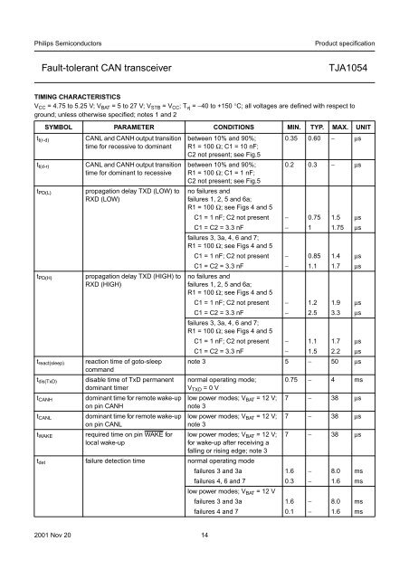
Philips SemiconductorsProduct specification<strong>Fault</strong>-<strong>tolerant</strong> <strong>CAN</strong> <strong>transceiver</strong><strong>TJA1054</strong>TIMING CHARACTERISTICSV CC = 4.75 to 5.25 V; V BAT = 5 to 27 V; V STB =V CC ; T vj = −40 to +150 °C; all voltages are defined with respect toground; unless otherwise specified; notes 1 and 2t t(r-d)t t(d-r)t PD(L)t PD(H)SYMBOL PARAMETER CONDITIONS MIN. TYP. MAX. UNITt react(sleep)t dis(TxD)t <strong>CAN</strong>Ht <strong>CAN</strong>Lt WAKE<strong>CAN</strong>L and <strong>CAN</strong>H output transitiontime for recessive to dominant<strong>CAN</strong>L and <strong>CAN</strong>H output transitiontime for dominant to recessivepropagation delay TXD (LOW) toRXD (LOW)propagation delay TXD (HIGH) toRXD (HIGH)reaction time of goto-sleepcommanddisable time of TxD permanentdominant timerdominant time for remote wake-upon pin <strong>CAN</strong>Hdominant time for remote wake-upon pin <strong>CAN</strong>Lrequired time on pin WAKE forlocal wake-upbetween 10% and 90%;R1 = 100 Ω; C1 = 10 nF;C2 not present; see Fig.5between 10% and 90%;R1 = 100 Ω; C1 = 1 nF;C2 not present; see Fig.50.35 0.60 − µs0.2 0.3 − µsno failures andfailures 1, 2, 5 and 6a;R1 = 100 Ω; see Figs 4 and 5C1 = 1 nF; C2 not present − 0.75 1.5 µsC1 = C2 = 3.3 nF − 1 1.75 µsfailures 3, 3a, 4, 6 and 7;R1 = 100 Ω; see Figs 4 and 5C1 = 1 nF; C2 not present − 0.85 1.4 µsC1 = C2 = 3.3 nF − 1.1 1.7 µsno failures andfailures 1, 2, 5 and 6a;R1 = 100 Ω; see Figs 4 and 5C1 = 1 nF; C2 not present − 1.2 1.9 µsC1 = C2 = 3.3 nF − 2.5 3.3 µsfailures 3, 3a, 4, 6 and 7;R1 = 100 Ω; see Figs 4 and 5C1 = 1 nF; C2 not present − 1.1 1.7 µsC1 = C2 = 3.3 nF − 1.5 2.2 µsnote 3 5 − 50 µsnormal operating mode;V TXD =0Vlow power modes; V BAT =12V;note 3low power modes; V BAT =12V;note 3low power modes; V BAT =12V;for wake-up after receiving afalling or rising edge; note 30.75 − 4 ms7 − 38 µs7 − 38 µs7 − 38 µst det failure detection time normal operating modefailures 3 and 3a 1.6 − 8.0 msfailures 4, 6 and 7 0.3 − 1.6 mslow power modes; V BAT =12Vfailures 3 and 3a 1.6 − 8.0 msfailures 4 and 7 0.1 − 1.6 ms2001 Nov 20 14