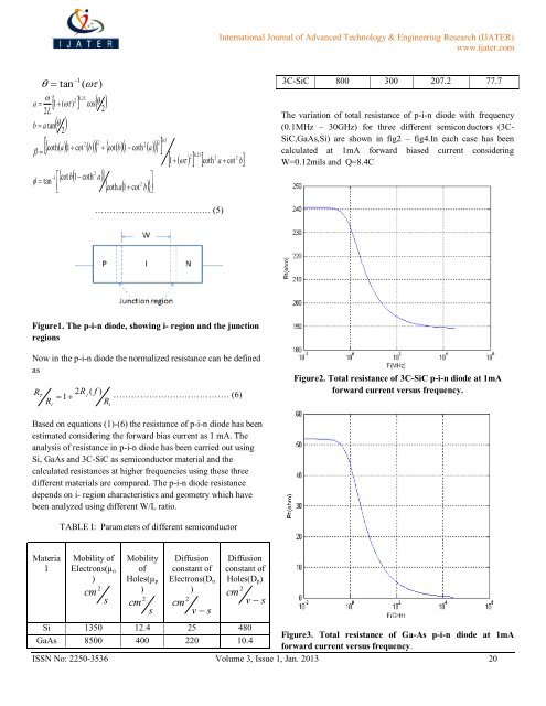
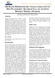
International Journal <strong>of</strong> Advanced Technology & Engineering Research (IJATER)www.<strong>ijater</strong>.com tan 1 ( )2 0.25a 1( ) cos 2L2b a tan2 tan 2 22cotha1 cot b cotb1 coth a12 cot b 1coth acoth a 1cot2b 20.52 0.25221 cotha cot b3C-SiC 800 300 207.2 77.7The variation <strong>of</strong> total resistance <strong>of</strong> p-i-n <strong>diode</strong> with frequency(0.1MHz – 30GHz) for three <strong>different</strong> semiconductors (3C-SiC,GaAs,Si) are shown in fig2 – fig4.In each case has beencalculated at 1mA forward biased current consideringW=0.12mils and Q=8.4C………………………………… (5)Figure1. The p-i-n <strong>diode</strong>, showing i- region and the junctionregionsNow in the p-i-n <strong>diode</strong> the normalized resistance can be definedasR 2R( f )TRj 1 ………………………………… (6)iRiFigure2. Total resistance <strong>of</strong> 3C-SiC p-i-n <strong>diode</strong> at 1mAforward current versus frequency.Based on equations (1)-(6) the resistance <strong>of</strong> p-i-n <strong>diode</strong> has beenestimated considering the forward bias current as 1 mA. Theanalysis <strong>of</strong> resistance in p-i-n <strong>diode</strong> has been carried out <strong>using</strong>Si, GaAs and 3C-SiC as semiconductor material and thecalculated resistances at higher frequencies <strong>using</strong> these three<strong>different</strong> materials are compared. The p-i-n <strong>diode</strong> resistancedepends on i- region <strong>characteristics</strong> and geometry which havebeen analyzed <strong>using</strong> <strong>different</strong> W/L ratio.TABLE I: Parameters <strong>of</strong> <strong>different</strong> semiconductorMaterialMobility <strong>of</strong>Electrons(µ n)cm 2sMobility<strong>of</strong>Holes(µ p)cm 2sDiffusionconstant <strong>of</strong>Electrons(D n)2cmv sDiffusionconstant <strong>of</strong>Holes(D p )2cmv sSi 1350 12.4 25 480GaAs 8500 400 220 10.4Figure3. Total resistance <strong>of</strong> Ga-As p-i-n <strong>diode</strong> at 1mAforward current versus frequency.ISSN No: 2250-3536 Volume 3, Issue 1, Jan. 2013 20
International Journal <strong>of</strong> Advanced Technology & Engineering Research (IJATER)www.<strong>ijater</strong>.com3. Result and AnalysisThe p-i-n switch shows that irrespective <strong>of</strong> base material it can<strong>of</strong>fer better <strong>switching</strong> action. In SiC the <strong>of</strong>f resistance is highercompare to GaAs and Si where as the band gap energy, meltingtemperature and other properties <strong>of</strong> SiC are more suitable for itsapplication as SPST switch at higher frequency (~30 GHz ormore). The normalized resistance <strong>of</strong> switch shows that (W/L)ratio has an important contribution to control the resistance<strong>characteristics</strong>. This is also evident from equation (6). With thediffusion length increase the resistance become low but thetransition <strong>of</strong> switch is not sharp compare to higher value <strong>of</strong>(W/L).This p-i-n <strong>diode</strong> can be used at higher frequency (~35 GHz) asSPST switch in Radar, Missile technology where number <strong>of</strong>IMPATT <strong>diode</strong>s are connected and the SPST switch controlsthem.Figure4. Total resistance <strong>of</strong> Si p-i-n <strong>diode</strong> at 1mA forwardcurrent versus frequency.Figure5. The normalized resistance for 3C-SiC p-i-n <strong>diode</strong>versus frequency-lifetime product fτ.Among these three materials SiC is WBG semiconductors and<strong>of</strong>fers better applications at microwave frequencies [7,8,9] thusthe normalized resistance <strong>of</strong> p-i-n <strong>diode</strong> has been calculated forSiC material only. The variation <strong>of</strong> normalized resistance as afunction <strong>of</strong> fτ is shown in fig.5 for <strong>different</strong> values <strong>of</strong> W/L.4. REFERENCES[1] Caverly,R.,Hiller, G., “Microwave resistance <strong>of</strong>Gallium Arsenide and Silicon p-i-n Diode”, IEEEMTT-S Digest,1987[2] A. Iturri-Hinojosa, L.M Resendize, and T.VTorchynska, “Numerical Analysis <strong>of</strong> the Performance<strong>of</strong> p-i-n Diode Microwave Switches Based onDifferent Semiconductor Materials”,Int.J.pureAppl.sci,Technology,2010.[3] Emmanull Gated, et.al., “An improved physics- BasedFormulation <strong>of</strong> the Microwave p-i-n <strong>diode</strong>impedance”, IEEE microwave and Wirelesscomponents Letters, Vol.17. No.3, March 2007.[4] D.Leenov, “The Silicon p-i-n dode as a microwaverader protector at megawatt levels”, IEEE Trans.Electron Devices, Vol. ED-11, no.2, PP.53-61, Feb.1964.[5] R.H. Caverly and G. Hiller “The small signal acimpedance <strong>of</strong> gallium arsenide and silicon p-i-n<strong>diode</strong>”, solid state electron, Vol.33, no.10, PP.1255-1263,1990.[6] Size, S.M., “Physics <strong>of</strong> Semiconductor Devices”, JhonWilly and Sons, New York, 1989.[7] M.Ray Kanjilal, D.Ghosh, M. Mukherjee, “Studies <strong>of</strong>Electrical Characteristics <strong>of</strong> MESFET Using WBG IV-IV SiC AS Potential Substrate Material”, IJSAT, Vol2 no 6, PP. 71 – 76, June 2012.ISSN No: 2250-3536 Volume 3, Issue 1, Jan. 2013 21