switching characteristics of pin diode using different ... - ijater
switching characteristics of pin diode using different ... - ijater
switching characteristics of pin diode using different ... - ijater
Create successful ePaper yourself
Turn your PDF publications into a flip-book with our unique Google optimized e-Paper software.
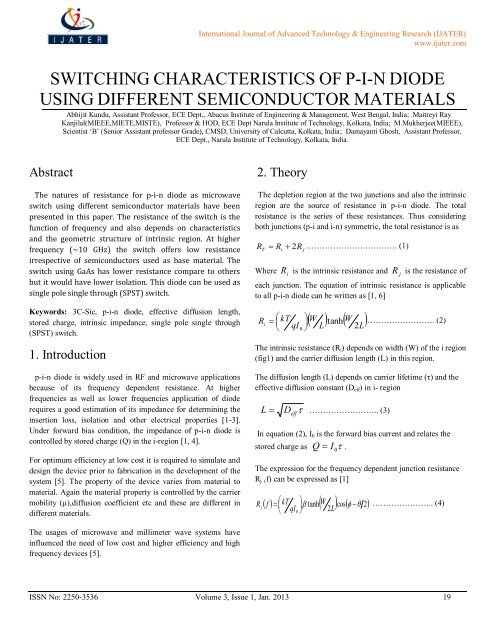
International Journal <strong>of</strong> Advanced Technology & Engineering Research (IJATER)www.<strong>ijater</strong>.com tan 1 ( )2 0.25a 1( ) cos 2L2b a tan2 tan 2 22cotha1 cot b cotb1 coth a12 cot b 1coth acoth a 1cot2b 20.52 0.25221 cotha cot b3C-SiC 800 300 207.2 77.7The variation <strong>of</strong> total resistance <strong>of</strong> p-i-n <strong>diode</strong> with frequency(0.1MHz – 30GHz) for three <strong>different</strong> semiconductors (3C-SiC,GaAs,Si) are shown in fig2 – fig4.In each case has beencalculated at 1mA forward biased current consideringW=0.12mils and Q=8.4C………………………………… (5)Figure1. The p-i-n <strong>diode</strong>, showing i- region and the junctionregionsNow in the p-i-n <strong>diode</strong> the normalized resistance can be definedasR 2R( f )TRj 1 ………………………………… (6)iRiFigure2. Total resistance <strong>of</strong> 3C-SiC p-i-n <strong>diode</strong> at 1mAforward current versus frequency.Based on equations (1)-(6) the resistance <strong>of</strong> p-i-n <strong>diode</strong> has beenestimated considering the forward bias current as 1 mA. Theanalysis <strong>of</strong> resistance in p-i-n <strong>diode</strong> has been carried out <strong>using</strong>Si, GaAs and 3C-SiC as semiconductor material and thecalculated resistances at higher frequencies <strong>using</strong> these three<strong>different</strong> materials are compared. The p-i-n <strong>diode</strong> resistancedepends on i- region <strong>characteristics</strong> and geometry which havebeen analyzed <strong>using</strong> <strong>different</strong> W/L ratio.TABLE I: Parameters <strong>of</strong> <strong>different</strong> semiconductorMaterialMobility <strong>of</strong>Electrons(µ n)cm 2sMobility<strong>of</strong>Holes(µ p)cm 2sDiffusionconstant <strong>of</strong>Electrons(D n)2cmv sDiffusionconstant <strong>of</strong>Holes(D p )2cmv sSi 1350 12.4 25 480GaAs 8500 400 220 10.4Figure3. Total resistance <strong>of</strong> Ga-As p-i-n <strong>diode</strong> at 1mAforward current versus frequency.ISSN No: 2250-3536 Volume 3, Issue 1, Jan. 2013 20
International Journal <strong>of</strong> Advanced Technology & Engineering Research (IJATER)www.<strong>ijater</strong>.com3. Result and AnalysisThe p-i-n switch shows that irrespective <strong>of</strong> base material it can<strong>of</strong>fer better <strong>switching</strong> action. In SiC the <strong>of</strong>f resistance is highercompare to GaAs and Si where as the band gap energy, meltingtemperature and other properties <strong>of</strong> SiC are more suitable for itsapplication as SPST switch at higher frequency (~30 GHz ormore). The normalized resistance <strong>of</strong> switch shows that (W/L)ratio has an important contribution to control the resistance<strong>characteristics</strong>. This is also evident from equation (6). With thediffusion length increase the resistance become low but thetransition <strong>of</strong> switch is not sharp compare to higher value <strong>of</strong>(W/L).This p-i-n <strong>diode</strong> can be used at higher frequency (~35 GHz) asSPST switch in Radar, Missile technology where number <strong>of</strong>IMPATT <strong>diode</strong>s are connected and the SPST switch controlsthem.Figure4. Total resistance <strong>of</strong> Si p-i-n <strong>diode</strong> at 1mA forwardcurrent versus frequency.Figure5. The normalized resistance for 3C-SiC p-i-n <strong>diode</strong>versus frequency-lifetime product fτ.Among these three materials SiC is WBG semiconductors and<strong>of</strong>fers better applications at microwave frequencies [7,8,9] thusthe normalized resistance <strong>of</strong> p-i-n <strong>diode</strong> has been calculated forSiC material only. The variation <strong>of</strong> normalized resistance as afunction <strong>of</strong> fτ is shown in fig.5 for <strong>different</strong> values <strong>of</strong> W/L.4. REFERENCES[1] Caverly,R.,Hiller, G., “Microwave resistance <strong>of</strong>Gallium Arsenide and Silicon p-i-n Diode”, IEEEMTT-S Digest,1987[2] A. Iturri-Hinojosa, L.M Resendize, and T.VTorchynska, “Numerical Analysis <strong>of</strong> the Performance<strong>of</strong> p-i-n Diode Microwave Switches Based onDifferent Semiconductor Materials”,Int.J.pureAppl.sci,Technology,2010.[3] Emmanull Gated, et.al., “An improved physics- BasedFormulation <strong>of</strong> the Microwave p-i-n <strong>diode</strong>impedance”, IEEE microwave and Wirelesscomponents Letters, Vol.17. No.3, March 2007.[4] D.Leenov, “The Silicon p-i-n dode as a microwaverader protector at megawatt levels”, IEEE Trans.Electron Devices, Vol. ED-11, no.2, PP.53-61, Feb.1964.[5] R.H. Caverly and G. Hiller “The small signal acimpedance <strong>of</strong> gallium arsenide and silicon p-i-n<strong>diode</strong>”, solid state electron, Vol.33, no.10, PP.1255-1263,1990.[6] Size, S.M., “Physics <strong>of</strong> Semiconductor Devices”, JhonWilly and Sons, New York, 1989.[7] M.Ray Kanjilal, D.Ghosh, M. Mukherjee, “Studies <strong>of</strong>Electrical Characteristics <strong>of</strong> MESFET Using WBG IV-IV SiC AS Potential Substrate Material”, IJSAT, Vol2 no 6, PP. 71 – 76, June 2012.ISSN No: 2250-3536 Volume 3, Issue 1, Jan. 2013 21
International Journal <strong>of</strong> Advanced Technology & Engineering Research (IJATER)www.<strong>ijater</strong>.com[8] Alicja Konczakowska, Jacek Cichosk, D. Dokupil,P.Flisikowski, “ The Low Frequency Noise Behaviour<strong>of</strong> SiC MESFETs”, 21 st International Cn<strong>of</strong>errence onNoise and Fluctation, IEEE, 2011.[9] J.W. Milligan, J.Henning, S.T. Allen, A.Ward, P.Parikh, R.P.Smith, “ Transition <strong>of</strong> SiC MESFETTechnology”, Cree, Inc., 4600 Silicon Drive, Durham,NC27703.BiographiesABHIJIT KUNDU received the B.Tech &M.tech degree in Electronics and Communication Engineeringfrom the University <strong>of</strong> W.B.U.T, Kolkata, West Bengal, in 2007&2010 respectively.Currently, He is an Assistant Pr<strong>of</strong>essor <strong>of</strong> Electronics andCommunication Engineering <strong>of</strong> Abacus Institute <strong>of</strong> Engineering &Management, West Bengal, India. His teaching and research areasinclude Microwave Engineering, Electro Magnetic Theory, SolidState Devices. Abhijit Kundu (Assistant Pr<strong>of</strong>essor) may bereached at abhijituday@yahoo.co.inDR. MAITREYI RAY KANJILAL is atpresent Pr<strong>of</strong>essor and Head in department <strong>of</strong>Electronics and Communication Engineeringat Narula Institute <strong>of</strong> Technology, Kolkata,West Bengal, India. She has a wide teachingexperience since 1998 in the colleges underC.U, Asansol engineering College, NarulaInstitute <strong>of</strong> Technology. She was also Head <strong>of</strong>the Department ECE and EIE departments at Techno IndiaCollege <strong>of</strong> Technology, Kolkata, India. She has received thePh.D from The University <strong>of</strong> Calcutta in the Year 2000. She isassociated with <strong>different</strong> universities for various academicactivities and also a life member <strong>of</strong> IETE, ISTE and Pr<strong>of</strong>essionalmember <strong>of</strong> IEEE (USA), IEEE-ED society (USA), IEEE-MTTs(USA). Her field <strong>of</strong> interest in research is low and highfrequency semiconductor devices and their applications,microelectronics and VLSI. Dr Ray Kanjilal is also the author <strong>of</strong>three books namely – Basic Electrical and ElectronicEngineering- Vol - 1 (Kolkata, West Bengal, JB Book andLearning, 2010), Basic Electrical and Electronic Engineering-Vol - 2 (Kolkata, West Bengal, JB Book and Learning, 2011)and Analog Electronic Circuits (Kolkata, West Bengal, JB Bookand Learning, 2012) and she has also reviewed books publishedby Pearson-Prentice Hall and Tata Mc Hill. Dr. Maitreyi RayKanjilal may be reached at mr.kanjilal@gmail.com.DR. MOUMITA MUKHERJEE hasreceived M.Sc. degree in Physics withspecialization in Electronics andCommunication and Ph.D. (Tech) inRadio Physics and Electronics fromUniversity <strong>of</strong> Calcutta, India. During June2003 to June 2010, she worked first as aSenior Research Fellow (SRF) and then as a Research Associate<strong>of</strong> Defence Research and Development Organization (DRDO),Ministry <strong>of</strong> Defence, New Delhi, India. She is presently workingas „Scientist –B‟ (Sr. Assistant Pr<strong>of</strong>.) at CMSDS, a centre <strong>of</strong>DRDO and University <strong>of</strong> Calcutta.Her research interest is focused on the modeling/simulation andfabrication <strong>of</strong> Millimeter and Sub-millimeter (Terahertz) wavehigh power homo-junction/hetero-junction devices based onwide-band-gap semiconductors, photonics, nano-scale THzdevices. She is the principal author <strong>of</strong> more than 100 peerreviewedresearch papers on semiconductor devices in reputedInternational refereed journals and reviewed IEEE-Proceedings.She is the author <strong>of</strong> 8 invited international book-chapters andworked as a Chief Editor <strong>of</strong> 2 books published from UK. Dr.Mukherjee is the „Technical-Reviewer” <strong>of</strong> a number <strong>of</strong> reputedinternational journals in India and abroad. Dr. Mukherjee hasreceived a number <strong>of</strong> international awards by Int. BiographicalCentre, IBC, UK, American Biographical Centre, USA, andMarque‟s Who‟s Who, USA. She has received “IEEE BestPaper Award” two times in 2009 and 2010. Dr. Mukherjee is themember <strong>of</strong> IEEE (USA), IEEE-ED society (USA), IEEE-MTTs(USA) and Indian Science Congress. Dr. Moumita Mukherjeemay be reached at moumita_phys@yahoo.comDAMAYANTI GHOSH is associated asAssistant Pr<strong>of</strong>essor with the department <strong>of</strong>Electronics and Communication Engineeringat Narula Institute <strong>of</strong> Technology,Kolkata,India. She has received the M.Tech degree inRadio Physics and Electronics CU in 2009.She has published few papers on MESFETand her area <strong>of</strong> interest is high frequencydevices like MESFET, HEMT, IMPATT etc. Damayanti Ghoshmay be reached at ghoshdamayanti@rediffmail.comISSN No: 2250-3536 Volume 3, Issue 1, Jan. 2013 22


