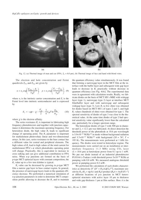
<str<strong>on</strong>g>HgCdTe</str<strong>on</strong>g> <str<strong>on</strong>g>epilayers</str<strong>on</strong>g> <strong>on</strong> <strong>GaAs</strong>: <strong>growth</strong> <strong>and</strong> <strong>devices</strong>Fig. 12. (a) Thermal image of man <strong>and</strong> car (FPA, l c = 6.0 µm), (b) Thermal image of face <strong>and</strong> h<strong>and</strong> with blood veins.The electr<strong>on</strong> <strong>and</strong> hole c<strong>on</strong>centrati<strong>on</strong> <strong>and</strong> Fermiquasilevels E Fn <strong>and</strong> E Fp are given byn = niæ E EE EFn - i öæ i - Fpöexp ç ÷ , p = niexp ç ÷ , (9)è k T øè k T øBwhere n i is the intrinsic carrier c<strong>on</strong>centrati<strong>on</strong> <strong>and</strong> E i is theFermi level into intrinsic semic<strong>on</strong>ductor <strong>and</strong> is expressedbyEiEg=-qj-c- -234BmnkBTln , (10)mwhere c is the electr<strong>on</strong> affinity.The series resistance R s is important in fabricating highfrequency photodetectors <strong>and</strong> together with juncti<strong>on</strong> capacitanceit determines the maximum operating frequency. Forheterodyne diode, the high value R s leads to significantchange of operating point. The R s parameter is importantfor multielement photovoltaic linear <strong>and</strong> two-dimensi<strong>on</strong>alarrays. In this case, series resistance to the base c<strong>on</strong>tact hasa different value for central <strong>and</strong> peripheral elements. Thehigh values of R s lead to high values of the total current formultielement FPA’s at which photodiodes operating pointwill change. Practically, this is equivalent to increase incross talking <strong>and</strong> can give additi<strong>on</strong>al c<strong>on</strong>tributi<strong>on</strong> to FPAnoise. When n-p juncti<strong>on</strong>s are formed <strong>on</strong> the basis ofp-type MCT epitaxial layers with c<strong>on</strong>stant compositi<strong>on</strong>, theR s value up to a few tens kilohm is typical.R s value can be decreased by growing in p-type MCTfilm a narrow gap layer in base c<strong>on</strong>tact regi<strong>on</strong>. In general,the presence of narrowgap layers leads to the quantum efficiencydecrease. We performed a numerical simulati<strong>on</strong> ofn-p juncti<strong>on</strong> parameters in order to determine MCT compositi<strong>on</strong>profile allowing to decrease the R s <strong>and</strong> to maintainpthe quantum efficiency value simultaneously. It was foundthat forming a narrowgap layer in the MCT film at the interfacewith the buffer layer <strong>and</strong> subsequent wide gap layerleads to decrease in R s practically without decrease inquantum efficiency [see Fig. 4(b)]. The experimental datawere in agreement with calculati<strong>on</strong> results. Really, we fabricatediodes <strong>on</strong> the basis of MCT HS’s MBE with widegaplayer (type 1), narrowgap (type 2) layer at interface MCTfilm/buffer layer <strong>and</strong> with narrowgap <strong>and</strong> subsequentwidegap layer (type 3). Low R s (a few ohm) was obtainedfor diodes based <strong>on</strong> MCT HS’s of types 2 <strong>and</strong> 3, <strong>and</strong> highR s values (hundreds of ohm) were obtained for type 1. Thespectral sensitivity of diodes of type 3 was close to the theoreticalvalue. At the same time diodes of type 2 had spectralsensitivity value significantly lower than the calculated<strong>on</strong>e, particularly for a l<strong>on</strong>ger spectrum range.The heterodyne diodes of type 3 with 300 µm in diameter<strong>and</strong> l c = 12.1 µm was fabricated. At direct detecti<strong>on</strong> thethreshold power of the photodiode at 10.6 µm wavelengthis 5.9×10 –14 W/Hz 1/2 in mode without background radiati<strong>on</strong><strong>and</strong> 3.7×10 –13 W/Hz 1/2 with background (2q =76°, T =195 K). The measurements were performed at 1 kHz frequency.The diodes were tested in heterodyne regime. Themeasurements were carried out <strong>on</strong> an installati<strong>on</strong> at intermediatefrequency 11.3 MHz using CO 2 laser(l = 10.6 µm) at heterodyne power from 0.1 up to 1 mW.We put our diode instead of an industrial photodetectorFUO144 («Tsukat») with threshold power 5×10 –20 W/Hz atpumping with 0.8 mW. We measured analogous thresholdpower at pumping power 0.2 mW.We performed the calculati<strong>on</strong> of such diodes characteristicsas detectivity D * [D * = R l (ADf/I n ) 1/2 ], maximum sensitivityR l (R l = hq/hc) <strong>and</strong> R 0 A product [R 0 A = A(dI/dV) –1 ]at different locati<strong>on</strong>s of p-n juncti<strong>on</strong> in MCT heteroepitaxialstructures with active layer 10 µm in thickness<strong>and</strong> wide gap thickness 1 µm at film surface. Here A is the108 Opto-Electr<strong>on</strong>. Rev., 11, no. 2, 2003 © 2003 COSiW SEP, Warsaw
C<strong>on</strong>tributed paperFig. 13. (a) The dependence of R l <strong>on</strong> p-n juncti<strong>on</strong> locati<strong>on</strong>. (b) The dependence of R 0 A products <strong>on</strong> p-n juncti<strong>on</strong> locati<strong>on</strong>. (c) Thedependence of D* <strong>on</strong> p-n juncti<strong>on</strong> locati<strong>on</strong>.diodes area, Df is the frequency b<strong>and</strong>, I n is the noise current,h is the quantum efficiency, <strong>and</strong> q is the electr<strong>on</strong>charge.MCT compositi<strong>on</strong> in active layer was X CdTe = 0.22,0.25, <strong>and</strong> 0.3. The n-p juncti<strong>on</strong> locati<strong>on</strong> varied from themiddle part of the diode to its surface. The carrier c<strong>on</strong>centrati<strong>on</strong>value is 10 16 cm –3 in p-type regi<strong>on</strong> <strong>and</strong> 10 17 cm –3 inn-type <strong>on</strong>e. The n-p juncti<strong>on</strong> is assumed to be abrupt. Thestructure was illuminated from the substrate side.The calculati<strong>on</strong> results [36] for R l , R 0 A <strong>and</strong> D* dependencies<strong>on</strong> the positi<strong>on</strong> of n <strong>on</strong> p (n-p) juncti<strong>on</strong> (Z p-n ) for differentX CdTe are presented in Figs. 13(a), 13(b) <strong>and</strong> 13(c)(solid lines). Independently <strong>on</strong> X CdTe in the active layer asharp decrease in R l <strong>and</strong> increase in R 0 A product was observedwhen n-p juncti<strong>on</strong> locati<strong>on</strong> is close to the surface regi<strong>on</strong>(~1 µm). However, increase in R 0 A product takesplace faster than decreasing R l . So, this leads to appearanceof maximum in D* at 0.7–0.8 µm from the film surface.The D * maximum is 3.5 times higher than D * in case of n-pjuncti<strong>on</strong> locati<strong>on</strong> in the active layer with c<strong>on</strong>stant X CdTe =0.3. It is interesting to note that with significant R 0 A increasethere is observed a relatively low decrease in D *value. Thus, for X CdTe = 0.22, at n-p juncti<strong>on</strong> locati<strong>on</strong> at0.4 µm from the surface, the R 0 A product is 30 times higherthan for n-p juncti<strong>on</strong> locati<strong>on</strong> in active layer with D * being<strong>on</strong>ly in 5.5 times lower. For MCT HS’s structures withX CdTe = 0.25 R 0 A value increases 110 times with D * being2.5 times lower.Analogous characteristics of R l ,R 0 A <strong>and</strong> D * were calculatedfor p <strong>on</strong> n (p-n) juncti<strong>on</strong> with doping level in n-type10 15 cm –3 <strong>and</strong> in p-type 10 16 cm –3 [Figs. 11(a), 11(b) <strong>and</strong>11(c) – dashed lines]. Some different features were observedfor p-n structures. The change of R 0 A product variessignificantly less at the p-n juncti<strong>on</strong> shift to the graded gapregi<strong>on</strong> than for n-p structures. Furthermore, at X CdTe = 0.22slow increase in R 0 A begins even in the active layer. Forall X CdTe the R l value in p-n structures increases steadilywith the p-n juncti<strong>on</strong> shift to the surface <strong>and</strong> then decreasesdramatically in the graded gap regi<strong>on</strong>. The D * value increaseswhen p-n juncti<strong>on</strong> is shifted to the surface <strong>and</strong>achieves maximum in the graded gap regi<strong>on</strong>. The subsequentD * decrease for p-<strong>on</strong>-n structures is weaker than forn-<strong>on</strong>-p <strong>on</strong>es.Thus, numerical calculati<strong>on</strong>s dem<strong>on</strong>strate the possibilityof improving the characteristics of the photodiodesbased <strong>on</strong> MCT graded gap layers when the n-p juncti<strong>on</strong>is formed in the graded gap regi<strong>on</strong>. The p-n photodiodesoffer some advantages over the n-p diodes.5. C<strong>on</strong>clusi<strong>on</strong>sThe basic <strong>and</strong> specific physical <strong>and</strong> chemical features atMCT heterostructure <strong>growth</strong> <strong>on</strong> <strong>GaAs</strong> substrates <strong>and</strong> defectsformati<strong>on</strong> mechanisms were discussed. The waysof decreasing defects to minimal values <strong>and</strong> growingMCT films of high quality <strong>on</strong> <strong>GaAs</strong> substrate were determined.A new generati<strong>on</strong> of industrially oriented ultra highvacuum set for MBE <strong>growth</strong> of MCT HS’s with in situellipso-metric c<strong>on</strong>trol <strong>and</strong> automated c<strong>on</strong>trol of technologicalprocesses was developed <strong>and</strong> produced.The industrially oriented technology of MCT HS’sMBE <strong>growth</strong> <strong>on</strong> 2’’ (013)<strong>GaAs</strong> substrate for multielementphotodiodes <strong>and</strong> photoc<strong>on</strong>ductors arrays was developed.Single, linear <strong>and</strong> focal plane arrays of high qualitywere fabricated <strong>on</strong> the basis of MCT heterostructures <strong>on</strong><strong>GaAs</strong>. Calculati<strong>on</strong> <strong>and</strong> experimental results of detectorcharacteristics revealed improving series resistance in diodesfabricating <strong>on</strong> the basis of MCT films with narrowgaplayer. The increase in detectivity was found at optimal p-njuncti<strong>on</strong> locati<strong>on</strong> at graded widegap layer near the MCTfilm surface.Opto-Electr<strong>on</strong>. Rev., 11, no. 2, 2003 V.S. Varavin 109