HgCdTe epilayers on GaAs: growth and devices
HgCdTe epilayers on GaAs: growth and devices
HgCdTe epilayers on GaAs: growth and devices

You also want an ePaper? Increase the reach of your titles
YUMPU automatically turns print PDFs into web optimized ePapers that Google loves.
C<strong>on</strong>tributed paperOPTO-ELECTRONICS REVIEW 11(2), 99–111 (2003)<str<strong>on</strong>g>HgCdTe</str<strong>on</strong>g> <str<strong>on</strong>g>epilayers</str<strong>on</strong>g> <strong>on</strong> <strong>GaAs</strong>: <strong>growth</strong> <strong>and</strong> <strong>devices</strong>V.S. VARAVIN, V.V. VASILIEV, S.A. DVORETSKY * , N.N. MIKHAILOV, V.N. OVSYUK,YU.G. SIDOROV, A.O. SUSLYAKOV, M.V. YAKUSHEV, <strong>and</strong> A.L. ASEEVInstitute of Semic<strong>on</strong>ductor Physics SB RAS, 13 Lavrentieva Av., 630090 Novosibirsk, RussiaView of basic <strong>and</strong> specific physical <strong>and</strong> chemical features of <strong>growth</strong> <strong>and</strong> defect formati<strong>on</strong> in mercury cadmium telluride(MCT) heterostructures (HS’s) <strong>on</strong> <strong>GaAs</strong> substrates by molecular beam epitaxy (MBE) was made. On the basis of this knowledgea new generati<strong>on</strong> of ultra high vacuum set, ultra-fast ellipsometer of high accuracy <strong>and</strong> automatic system for c<strong>on</strong>trol oftechnological processes was produced for reproducibility of <strong>growth</strong> MCT Hs’s <strong>on</strong> substrates up to 4” in diameter. The developmentof industrially oriented technology of MCT HS’s <strong>growth</strong> by MBE <strong>on</strong> <strong>GaAs</strong> substrates 2” in diameter <strong>and</strong> withoutintenti<strong>on</strong>al doping is presented. The electrical characteristics of n-type <strong>and</strong> p-type of MCT HS’s <strong>and</strong> uniformity of MCTcompositi<strong>on</strong> over the surface area are excellent. The residual d<strong>on</strong>or <strong>and</strong> acceptor centres are supposed as hypotheticallytellurium atoms in metallic sublattice (“antisite” tellurium) <strong>and</strong> double-i<strong>on</strong>ised mercury vacancies. The technology of fabricatingfocal plane arrays is developed. The high quality characteristics of infrared detectors c<strong>on</strong>ductance <strong>and</strong> diode modeare measured. Calculati<strong>on</strong>s of detector parameters predicted the improvement in serial resistance <strong>and</strong> detectivity of infrareddiode detectors based <strong>on</strong> MCT heterostructures with graded compositi<strong>on</strong> throughout the thickness.Keywords: MCT, MBE, <strong>growth</strong> <strong>GaAs</strong>, Si, ellipsometer, heterostructures, infrared detectors, photoc<strong>on</strong>ductors,photodiodes, focal plane arrays, p-n juncti<strong>on</strong>s.1. Introducti<strong>on</strong>Cd x Hg 1–x Te (MCT) solid soluti<strong>on</strong> is the basic material forinfrared detectors (IRD) that operate in a wide wavelengthrange (from 1 to 20 µm <strong>and</strong> over). The lattice c<strong>on</strong>stant ofMCT is weekly changed for different compositi<strong>on</strong>s betweenCdTe <strong>and</strong> HgTe. This is very important for usingcomplex MCT heterostructutres (HS’s) for a new generati<strong>on</strong>of IRD. Using different physical processes enables usto design different types of IRD operating in a wide temperaturerange (from liquid nitrogen temperature to room<strong>on</strong>e).The future development of multielement IRD needs increasein substrate dimensi<strong>on</strong> <strong>and</strong> uniformity of physicalproperties over the surface area. Now the basic research isfocused <strong>on</strong> the <strong>growth</strong>, doping <strong>and</strong> characterizati<strong>on</strong> ofMCT <strong>on</strong> lattice matched CdZnTe substrates because thehighest crystal perfecti<strong>on</strong> is realized just for this materialc<strong>on</strong>jugati<strong>on</strong>. CdZnTe substrates of a large area (up to40×60 mm 2 ) are available <strong>and</strong> used for MCT <strong>growth</strong>. Butthe crystal perfecti<strong>on</strong> <strong>and</strong> Zn c<strong>on</strong>tent are not uniform overthe surface area [1]. Additi<strong>on</strong>ally, the disadvantages ofCdZnTe substrates are high cost, absence of precise impurityc<strong>on</strong>trol at <strong>growth</strong>, essential difference of coefficient ofthermal expansi<strong>on</strong> from silic<strong>on</strong> <strong>on</strong>es <strong>and</strong> low mechanicalstrength.* e-mail: dvor@isp.nsc.ruThe alternative substrates (<str<strong>on</strong>g>epilayers</str<strong>on</strong>g> of CdTe orCdZnTe <strong>on</strong> Al 2 O 3 , <strong>GaAs</strong>, Si substrate, etc.) have the advantagesin comparis<strong>on</strong> with CdZnTe substrates from thepoint of view of substrate dimensi<strong>on</strong>, low cost <strong>and</strong> coefficientsof thermal expansi<strong>on</strong> are practically equal to the parametersof silic<strong>on</strong> which is used for producti<strong>on</strong> of read-outcircuits. The most attractive from alternative substrates arethose based <strong>on</strong> <strong>GaAs</strong> [2–4] <strong>and</strong> Si [5–7]. The disadvantagesof such substrates are the large lattice mismatch ofc<strong>on</strong>jugati<strong>on</strong> materials which is equal to ~14.6% forCdTe/<strong>GaAs</strong> <strong>and</strong> ~19% for CdTe/Si at room temperatures.This leads to decrease of MCT crystalline perfecti<strong>on</strong> incomparis<strong>on</strong> with the use of CdZnTe substrates. The MCTquality <strong>on</strong> <strong>GaAs</strong> must be better than that for MCT <strong>on</strong> Si.The advantage of using Si substrates for <strong>growth</strong> of MCTHS’s is the possibility of creating photosensitive MCTepilayer <strong>and</strong> read-out circuit in m<strong>on</strong>olithic hybridisati<strong>on</strong>scheme.The most attractive method for growing MCT epitaxialmaterial is MBE technique because of its flexibility, simplicity<strong>and</strong> many advantages over the others techniques.There is dem<strong>on</strong>strated the fabricati<strong>on</strong> of SWIR [8], MWIR[9], LWIR [10] <strong>and</strong> VLWIR [11] detectors <strong>on</strong> the basis ofMCT HS’s grown <strong>on</strong> CdZnTe, <strong>GaAs</strong> by MBE with thephotoelectrical characteristics compared with analogous<strong>on</strong>es for IRD <strong>on</strong> basis of MCT <str<strong>on</strong>g>epilayers</str<strong>on</strong>g> grown by LPE <strong>and</strong>MOVPE. From MCT HS’s MBE <strong>on</strong> Si <strong>on</strong>ly MWIR <strong>devices</strong>with high quality characteristics were fabricated now.The parameters of IRD depend <strong>on</strong> crystalline perfecti<strong>on</strong> ofOpto-Electr<strong>on</strong>. Rev., 11, no. 2, 2003 V.S. Varavin 99
<str<strong>on</strong>g>HgCdTe</str<strong>on</strong>g> <str<strong>on</strong>g>epilayers</str<strong>on</strong>g> <strong>on</strong> <strong>GaAs</strong>: <strong>growth</strong> <strong>and</strong> <strong>devices</strong>MCT material. The dislocati<strong>on</strong> density (Nd) essentially influences<strong>on</strong> parameters of LWIR diodes detectors [12,13]which operated at low temperatures. The calculati<strong>on</strong>showed that for LWIR regi<strong>on</strong> R 0 A product at 77 K wasstr<strong>on</strong>gly dependent <strong>on</strong> dislocati<strong>on</strong> densities over 10 6 cm –2[14]. The dislocati<strong>on</strong> density of MCT HS’s <strong>on</strong> <strong>GaAs</strong> substrateafter the <strong>growth</strong> is at level near 10 6 cm –2 <strong>and</strong> over <strong>and</strong>decrease up to 2×10 5 cm –2 after annealing at elevated temperatures[15]. This means that it is possible to grow MCTHS’s <strong>on</strong> <strong>GaAs</strong> which is suitable for fabricating diode typeIRD. Earlier, it was shown that the minority carrier lifetimet of n-type MCT HS’s <strong>on</strong> <strong>GaAs</strong> substrates without widegaplayer at boundaries was 220 ns at minimal dislocati<strong>on</strong> density<strong>and</strong> decrease up to few tens with increasing dislocati<strong>on</strong>density. We showed that the minority lifetime at dislocati<strong>on</strong>density 5×10 7 cm –2 is close to 1000 ns for MCT HS’s<strong>on</strong> <strong>GaAs</strong> with a widegap layer at film boundaries [16].These values are two orders higher than for MCT HS’s <strong>on</strong><strong>GaAs</strong> without a wide gap layer. So, MCT HS’s withwidegap layer may be used for fabricating photoc<strong>on</strong>ductors.The important parameter at fabricating photovoltaicIRD is minority carrier lifetime. The minority carrier lifetimedetermines the diffusi<strong>on</strong> length <strong>and</strong> dark current of adiode. MCT bulk crystal or <str<strong>on</strong>g>epilayers</str<strong>on</strong>g> of p-type c<strong>on</strong>ductivityfor photovoltaic IRD are fabricated by thermal annealing ofas-grown material. The minority lifetime of LWIR MCT isup to 10–20 nanosec<strong>on</strong>ds <strong>and</strong> is limited by double i<strong>on</strong>isedmercury vacancies [17,18]. The values of diffusi<strong>on</strong> length(optical area of diode) of minority carriers (electr<strong>on</strong> inp-type MCT) for t = 10 ns <strong>and</strong> different mobilities are presentedin Table 1.Table 1. The values of diffusi<strong>on</strong> length of electr<strong>on</strong> in p-typeMCT.t (ns) µ (cm 2 /Vs) L (µm)10 10000 8.010 50000 17,910 100000 25.3It can be seen that p-type MCT material may be usedfor producti<strong>on</strong> of photovoltaic focal plane arrays whichpixel dimensi<strong>on</strong>s <strong>and</strong> pitches are compared with diffusi<strong>on</strong>length. The modern tendencies are decreasing the FPA’spixel dimensi<strong>on</strong>s <strong>and</strong> pitches <strong>and</strong> increasing number of elements.So, p-type MCT HS’s MBE fabricating by annealingare suitable for producti<strong>on</strong> of FPA’s with small pixeldimensi<strong>on</strong>s <strong>and</strong> pitches. It is necessary to remark that forsuch FPA’s <strong>on</strong>e can eliminate cross talking between neighbouringdiodes.The purpose of this paper is the overview of progress<strong>on</strong> development of industrially oriented equipment, c<strong>on</strong>troltechnique <strong>and</strong> technology of <strong>growth</strong> process of MCT HS’sby MBE <strong>on</strong> <strong>GaAs</strong> substrates, technology of fabricating focalplane arrays <strong>and</strong> characteristics of infrared photoc<strong>on</strong>ductors<strong>and</strong> photodiodes.2. Epilayers <strong>growth</strong>2.1. Basic features of MCT <strong>growth</strong> by MBEMBE is a developed <strong>and</strong> widely used epitaxial method for<strong>growth</strong> of narrow-gap mercury c<strong>on</strong>tent A 2 B 6 HS’s <strong>and</strong>,first of all, for <strong>growth</strong> of MCT <strong>on</strong> CdZnTe <strong>and</strong> alternativesubstrates. The status of MCT MBE technology hasreached the level for producing material used for industrialproducti<strong>on</strong> of high quality IR <strong>devices</strong>.MBE offers many advantages over other epitaxialmethods of MCT <strong>growth</strong> due to several reas<strong>on</strong>s:• MCT film <strong>growth</strong> is carried out at lowest temperatures(160°C–200°C) as compared with 450 ° C for LPE <strong>and</strong>250 ° C–400 ° C for MOVPE. The reducti<strong>on</strong> of <strong>growth</strong>temperature precludes impurity diffusi<strong>on</strong> from the substrateinto MCT films resulting in reducti<strong>on</strong> of the backgrounddoping down to 1–1.5 order at the same purityof material for MCT synthesis,• unlike in LPE, no aggressive medium is present inMBE that leads to use of alternative substrates,• the c<strong>on</strong>trol of <strong>growth</strong> <strong>and</strong> MCT films parameters in situgives possibility to fabricate structures with desiredMCT compositi<strong>on</strong> distributi<strong>on</strong> throughout the thicknessfor a multicolour IRD. The c<strong>on</strong>trol of MCT compositi<strong>on</strong>in situ allows to grow heterojuncti<strong>on</strong>s of top quality,• MBE is an ideal technique for growing CdTe/HgTesuperlattices <strong>and</strong> other nanostructures.The detailed investigati<strong>on</strong>s of physical <strong>and</strong> chemicalfoundati<strong>on</strong>s of <strong>growth</strong> process, mechanism of defect formati<strong>on</strong>,nature of residual doping for realisati<strong>on</strong> of evidentMBE advantages were carried out. It was found that thereexist the fundamental physical <strong>and</strong> chemical reas<strong>on</strong>s thatdetermine MCT film quality at <strong>growth</strong> by MBE. These reas<strong>on</strong>sare as follows:• relati<strong>on</strong>ship between equivalent beam pressures (EBP)of mercury <strong>and</strong> tellurium (P (ebpHg) /P (ebpTe2) ),• <strong>growth</strong> temperature,• substrate orientati<strong>on</strong>,• nature of tellurium in molecular flux.At a fixed substrate temperature <strong>and</strong> <strong>growth</strong> rate the intervalof optimal P (ebp Hg) /P (ebp Te2) is needed for MCT film<strong>growth</strong> with minimal defect densities, excellent electricalparameters [19]. At the fixed value of P (ebp Hg) /P (ebp Te2) <strong>and</strong><strong>growth</strong> rate there exists an interval of optimal temperaturesfor <strong>growth</strong> of crystalline perfecti<strong>on</strong> MCT films [19]. At deviati<strong>on</strong>of P (ebp Hg) /P (ebp Te2) <strong>and</strong> temperatures from optimal<strong>on</strong>es a sharp decrease in MCT film crystalline quality (increasein densities of surface defects, microtwins in volume,etc.), poor electrical parameters is observed. Thequality of MCT films depends <strong>on</strong> substrate orientati<strong>on</strong>. Itwas shown that the highest MCT film quality was reachedat <strong>growth</strong> <strong>on</strong> vicinal substrate orientati<strong>on</strong> even at high<strong>growth</strong> rates (up to 7–10 µm/h). The (112) substrate orientati<strong>on</strong>is mainly used for <strong>growth</strong> of MCT films. However,the range of <strong>growth</strong> c<strong>on</strong>diti<strong>on</strong>s (P (ebp Hg) /P (ebp Te2) <strong>and</strong> temperatures)is enough narrow for <strong>growth</strong> of high quality100 Opto-Electr<strong>on</strong>. Rev., 11, no. 2, 2003 © 2003 COSiW SEP, Warsaw
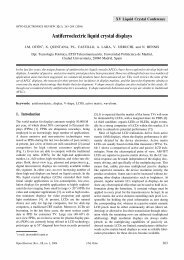
C<strong>on</strong>tributed paperMCT films. We found that the range of <strong>growth</strong> c<strong>on</strong>diti<strong>on</strong>smay be extended without decreasing MCT film quality at<strong>growth</strong> <strong>on</strong> (013) substrates.The important reas<strong>on</strong> of defect formati<strong>on</strong> during MCT<strong>growth</strong> by MBE is the nature of tellurium which existsmainly as diatomic molecules in a molecular flux. On a<strong>growth</strong> surface, diatomic tellurium molecules reacted withmercury <strong>and</strong> cadmium atoms with the crystallizati<strong>on</strong> ofMCT compound by the following reacti<strong>on</strong>s:• dissociati<strong>on</strong> of diatomic tellurium molecules <strong>on</strong>to atomsTe 2 (ads) ® 2Te (ads) ,• crystallisati<strong>on</strong> of mercury cadmium telluride compoundsCd (ads) +Te (ads) ® CdTe (s) ,Hg (ads) +Te (ads) ® HgTe (s) .Kinetic limitati<strong>on</strong>s of reacti<strong>on</strong>s at low temperatures ofMCT compound crystallisati<strong>on</strong> lead to formati<strong>on</strong> of telluriumsegregati<strong>on</strong>s <strong>and</strong> substituti<strong>on</strong> of cadmium <strong>and</strong> mercuryin metallic crystal sublattice by the following reacti<strong>on</strong>:• depositi<strong>on</strong> of tellurium in solid phaseTe 2 (ads) ® Te 2 (s) ,• incorporati<strong>on</strong> of diatomic molecules into crystal latticeTe 2 (ads.) ® Te (m) -Te.In the first case, tellurium depositi<strong>on</strong> in a solid phase isa reas<strong>on</strong> of V-defects (voids) formati<strong>on</strong>. In the sec<strong>on</strong>d case,tellurium <strong>on</strong> metallic site (Te (m) so-called “antisite” tellurium)is a probable residual d<strong>on</strong>or centre for MCT films<strong>growth</strong> by MBE.The scheme of crystallisati<strong>on</strong> processes of MCT filmswith diatomic tellurium molecules is shown in Fig. 1.Fig. 1. The scheme of crystallizati<strong>on</strong> processes of MCT films byMBE: 1 – dissociati<strong>on</strong> of diatomic Te molecules <strong>on</strong> atoms,2 – incorporati<strong>on</strong> of diatomic Te molecules in MCT crystal lattice,3 – depositi<strong>on</strong> of diatomic Te molecules in solid phase, 4 – reacti<strong>on</strong>sof Te atoms with cadmium <strong>and</strong> mercury for high quality MCT<strong>growth</strong>, 5 – formati<strong>on</strong> of V-defects (voids).The development <strong>and</strong> producti<strong>on</strong> of efficient equipment,c<strong>on</strong>trol technique of <strong>growth</strong> processes in situ, the<strong>growth</strong> technology (including MCT <strong>growth</strong> <strong>on</strong> large in dimensi<strong>on</strong><strong>GaAs</strong> <strong>and</strong> Si substrates) allows all advantages ofMBE to be realised <strong>and</strong> used in future for industrial MCTproducti<strong>on</strong>.2.2. Specific features at MCT <strong>growth</strong> <strong>on</strong> <strong>GaAs</strong>Specific features of MCT depositi<strong>on</strong> <strong>on</strong> <strong>GaAs</strong> substrate arethe basic features at depositi<strong>on</strong> of CdZnTe layers <strong>on</strong> <strong>GaAs</strong>.The depositi<strong>on</strong> of MCT films <strong>on</strong> <strong>GaAs</strong> substrate without abuffer layer at low temperatures did not allow the materialof required quality for device applicati<strong>on</strong> to grow. The essentialsuccess has been reached in MCT film <strong>growth</strong> <strong>on</strong>“alternative” substrates – CdZnTe buffer layer <strong>on</strong> <strong>GaAs</strong>substrate. The <strong>growth</strong> of ZnTe, CdTe or its compounds <strong>on</strong><strong>GaAs</strong> of good quality is c<strong>on</strong>nected with specific features ofdefect formati<strong>on</strong> at c<strong>on</strong>jugati<strong>on</strong> of II–VI <strong>and</strong> III–V compounds:• n<strong>on</strong>isovalency of c<strong>on</strong>jugati<strong>on</strong> of CdZnTe <strong>and</strong> <strong>GaAs</strong>substrates,• large mismatch between CdZnTe <strong>and</strong> <strong>GaAs</strong>,• doping of MCT by gallium from <strong>GaAs</strong> substrate.At c<strong>on</strong>jugati<strong>on</strong> of A 2 B 6 <strong>and</strong> A 3 B 5 , Si the excess of valenceelectr<strong>on</strong>s leads to distorti<strong>on</strong> of tetrahedral c<strong>on</strong>figurati<strong>on</strong>of a compound <strong>on</strong> the interface (formati<strong>on</strong> of two orthree atomic b<strong>on</strong>ds instead of four <strong>on</strong>es) <strong>and</strong> as a c<strong>on</strong>sequenceto change a layer orientati<strong>on</strong> from a substrate <strong>on</strong>e.Chemical interacti<strong>on</strong> <strong>on</strong> A 2 B 6 /<strong>GaAs</strong> interface at the initial<strong>growth</strong> stage plays a critical role in formati<strong>on</strong> of surfacemorphology <strong>and</strong> structural defects. The main reas<strong>on</strong> forthat is the change of average value of valence electr<strong>on</strong>s atthe interface up<strong>on</strong> substituti<strong>on</strong> of As by Te <strong>and</strong> formati<strong>on</strong>of Ga-Te b<strong>on</strong>ds in a crystal lattice. The tendency to eliminatethe excess of valence electr<strong>on</strong>s at the interface leads toformati<strong>on</strong> of facets, twins <strong>and</strong> change of stoichiometry of<strong>growth</strong> structure.A large mismatch of CdZnTe <strong>and</strong> <strong>GaAs</strong> is resp<strong>on</strong>siblefor disordered phase, dislocati<strong>on</strong>s <strong>and</strong> orientati<strong>on</strong> mixtureof grown film [20,21]. It was found that the <strong>growth</strong> temperatures,molecular flux intensities, substrate orientati<strong>on</strong>s influenced<strong>on</strong> facets formati<strong>on</strong>, twinning, stochiometricbreaking <strong>and</strong> formati<strong>on</strong> of disordered phase at the initialstage of CdTe <strong>growth</strong> <strong>on</strong> <strong>GaAs</strong> substrate. The followingtechnological operati<strong>on</strong>s allow dividing these problems as:• use of vicinal <strong>GaAs</strong> surface for creati<strong>on</strong> of a system ofregular nuclei <strong>growth</strong> centres,• c<strong>on</strong>trol of compound formati<strong>on</strong> <strong>and</strong> nucleati<strong>on</strong> at theinitial stage of <strong>growth</strong>,• <strong>growth</strong> of ZnTe film <strong>on</strong> atomic clean <strong>GaAs</strong> surface toprevent the appearance of the mixture of orientati<strong>on</strong>,• <strong>growth</strong> of CdTe films <strong>on</strong> ZnTe/<strong>GaAs</strong> surface with thethickness 5–7 µm,• accurate c<strong>on</strong>trol of optimal molecular fluxes <strong>and</strong> theirrelati<strong>on</strong>ships <strong>and</strong> substrate temperatures.The auto doping of MCT film at <strong>growth</strong> <strong>on</strong> CdZnTe/<strong>GaAs</strong> substrates by MBE was suggested by SIMS analysis.However, electrical parameters show no correlati<strong>on</strong> withGa c<strong>on</strong>tent in MCT film volume. In fact, the Ga c<strong>on</strong>tentinto MCT film volume exceeds the observed electr<strong>on</strong> c<strong>on</strong>centrati<strong>on</strong>.It means that Ga is incorporated in a neutral positi<strong>on</strong>in a crystalline lattice. The thermodynamic calculati<strong>on</strong>of equilibrium Ga c<strong>on</strong>centrati<strong>on</strong> versus temperatureOpto-Electr<strong>on</strong>. Rev., 11, no. 2, 2003 V.S. Varavin 101
<str<strong>on</strong>g>HgCdTe</str<strong>on</strong>g> <str<strong>on</strong>g>epilayers</str<strong>on</strong>g> <strong>on</strong> <strong>GaAs</strong>: <strong>growth</strong> <strong>and</strong> <strong>devices</strong>3. Industrially-oriented producti<strong>on</strong> of MCT<str<strong>on</strong>g>epilayers</str<strong>on</strong>g>3.1. EquipmentFig. 2. Dependencies of equilibrium electrically active Gac<strong>on</strong>centrati<strong>on</strong> in MCT <strong>on</strong> temperature <strong>and</strong> compositi<strong>on</strong>.dependence with the presence of Ga 2 Te 3 taking into accountwas carried out [22]. In Fig. 2, the equilibrium c<strong>on</strong>centrati<strong>on</strong>of electrically active Ga is shown.It was found that Ga c<strong>on</strong>centrati<strong>on</strong> sharply decreasedwith decreasing temperature <strong>and</strong> became lower than10 8 cm –3 at temperatures below 200°C for MCT compositi<strong>on</strong>X CdTe = 0.2. Annealing MCT films at the temperaturesover 300°C can lead to increase in electr<strong>on</strong> c<strong>on</strong>centrati<strong>on</strong>because of transiti<strong>on</strong> of Ga atoms in an electrically activestate. Really, electr<strong>on</strong> c<strong>on</strong>centrati<strong>on</strong> at 10 17 cm –3 level wasobserved <strong>on</strong> annealing at 500°C.Taking into account the basic <strong>and</strong> specific features ofMCT <strong>growth</strong> <strong>on</strong> <strong>GaAs</strong> substrates the equipment <strong>and</strong> technologyhas been developed for CdZnTe buffer layer <strong>growth</strong><strong>on</strong> <strong>GaAs</strong> substrate <strong>and</strong> following MCT films <strong>growth</strong> withminimal defect density by MBE method.Industrially oriented producti<strong>on</strong> is being developed formanufacturing trivial <strong>and</strong> novel type of MCT HS’s MBE<strong>on</strong> (013)<strong>GaAs</strong> substrates 2” in diameter for different typesof IRD.MCT HS’s MBE producti<strong>on</strong> is based <strong>on</strong> the followingelements:• new generati<strong>on</strong> of ultra high vacuum multichamber setequipped with big-capacity molecular beam sources for<strong>growth</strong> <strong>on</strong> a substrates up to 4” in diameter with highcompositi<strong>on</strong> uniformity over the surface area; precisebuilt-in ultrafast ellipsometer (UFE) for c<strong>on</strong>trol of filmparameters in situ <strong>and</strong> an automatic system for c<strong>on</strong>trolof technological processes,• technological operating sequences for producti<strong>on</strong> ofn-type <strong>and</strong> p-type MCT HS’s with the parameters neededfor qualitative photoc<strong>on</strong>ductors <strong>and</strong> photodiodes,• equipment for characterizati<strong>on</strong> of MCT HS’s parameters(compositi<strong>on</strong>, carriers c<strong>on</strong>centrati<strong>on</strong> <strong>and</strong> their mobility,lifetime, density of surface defects, etc.).Ultra high vacuum installati<strong>on</strong> includes three technologicalchambers, two loading-unloading chambers <strong>and</strong>modules for transport racks <strong>and</strong> laminar dust free box.A technological chamber for <strong>growth</strong> of buffer layer(BL) is equipped with ring-shaped Cd <strong>and</strong> Zn molecularbeam sources which are mounted coaxially with a cylindricaltype of tellurium molecular beam source <strong>and</strong>high-energy electr<strong>on</strong> diffracti<strong>on</strong> (HEED) system. A techno-Fig. 3. Ultra-fast in situ operating ellipsometer LEF-751.102 Opto-Electr<strong>on</strong>. Rev., 11, no. 2, 2003 © 2003 COSiW SEP, Warsaw
C<strong>on</strong>tributed paperlogical chamber for <strong>growth</strong> of MCT layer is equipped withring-shaped Cd molecular beam source which is mountedcoaxially with a cylindrical type of tellurium molecularbeam source <strong>and</strong> built-in UFE system. Molecular beamsources provide high uniformity of fluxes over a large areaat minimal c<strong>on</strong>sumpti<strong>on</strong> of evaporated high cost materials.The calculati<strong>on</strong> showed that at accurate positi<strong>on</strong>ing of molecularbeam sources MCT compositi<strong>on</strong> gradient over thesurface area must be not worse than 0.0002 cm –1 .Itisbetter by <strong>on</strong>e order of magnitude than uniformity of MCTcompositi<strong>on</strong> needed for multielement IRD.Automatic (AE) types LEF–751 [23] <strong>and</strong> LEF–755 areremarkable due to their high speed <strong>and</strong> accuracy. They areused for measurement of <strong>growth</strong> rate, compositi<strong>on</strong> <strong>and</strong> surfacemorphology during MCT HS <strong>growth</strong>. MCT film compositi<strong>on</strong>X CdTe is deduced from ellipsometric parameterY being measured by UFE. Surface morphology is c<strong>on</strong>trolledby the ellipsometric parameter D. The ultra-fastellipsometer (UFE) in situ LEF-751 is shown in Fig. 3.To achieve the highest speed of measurement at highaccuracy a new two-channel static ellipsometer system hasbeen designed where two measuring channels (amplitude<strong>and</strong> phase) were spatially divided. The first channel (polariser–sample–analyser:PSA 1 ) is intended for Y measurement,the sec<strong>on</strong>d <strong>on</strong>e (polariser–sample–compensator–analyser:PSCA 2 ) is intended for measurement of D.Laser beam, linearly polarised by the polariser P incidents<strong>on</strong>to the sample surface S. One part of the reflectedbeam is directed into the channel y by the total reflecti<strong>on</strong>prism R. The total reflecti<strong>on</strong> prism has no dichroism <strong>and</strong>does not include an error in y measurement. The sec<strong>on</strong>dbeam passes through the channel D without directi<strong>on</strong>change. Both channels are designed identically, except thecompensator C placed in channel D.In either channel the light beam is splitted by aWollast<strong>on</strong> prism employed as the analyser A 1 (A 2 ) into twoorthog<strong>on</strong>ally polarized beams. These beams strikephotosensing areas of two-element photodiodes producingelectrical signals I 1 , I 2 , I 3 , <strong>and</strong> I 4 . During measurement, thepolarizati<strong>on</strong> elements are fixed at the azimuth positi<strong>on</strong>:polariser P=45°, compensator C =45°. The analyser A 2 hastwo fixed positi<strong>on</strong>s: 0° <strong>and</strong> 45° for complete polarizati<strong>on</strong>measurement. The ellipsometric parameters y <strong>and</strong> D are calculatedfrom four signals using the following equati<strong>on</strong>sAbsence of movable parts <strong>and</strong> signal modulati<strong>on</strong> duringmeasurement has provided very high speed limited <strong>on</strong>ly byamplifier-digitalizing capability.The measurement time is mainly limited by digitisati<strong>on</strong>.If digitisati<strong>on</strong> time of ADC is 10 µs, the measurement of <strong>on</strong>epair of y <strong>and</strong> D from four electrical signals takes 40 µs. Thespeed of the ellipsometer is certainly not limited by thesevalues. Potentially the ellipsometer system allows measurementwith nanosec<strong>on</strong>d <strong>and</strong> picosec<strong>on</strong>d time resoluti<strong>on</strong>.Ellipsometers have the following performance specificati<strong>on</strong>for MCT film measurement:• absolute accuracy of film compositi<strong>on</strong> X CdTe measurement±0.005,• sensitivity to compositi<strong>on</strong> X CdTe variati<strong>on</strong> ±0.0005,• minimal film thickness to be measured 0.5 nm.3.2. TechnologyThe technology of MCT HS’s MBE producti<strong>on</strong> <strong>on</strong>(013)<strong>GaAs</strong> includes the following operati<strong>on</strong>s:• chemical etching of <strong>GaAs</strong> substrate,• thermal treatment of <strong>GaAs</strong> surface in arsenic flux invacuum,• <strong>growth</strong> of CdZnTe buffer layer <strong>on</strong> an atomic clean<strong>GaAs</strong> surface,• <strong>growth</strong> of MCT <strong>on</strong> a buffer layer.The high sensitivity <strong>and</strong> time resoluti<strong>on</strong> of UFE allowshigh-accuracy measuring of <strong>growth</strong> rate, thickness at<strong>growth</strong> of buffer <strong>and</strong> MCT layers, MCT compositi<strong>on</strong> <strong>and</strong>its changing under steady state <strong>growth</strong> c<strong>on</strong>diti<strong>on</strong>. At<strong>growth</strong> of MCT film <strong>on</strong> CdTe, the ellipsometric parametersD <strong>and</strong> y in D-y plane is represented by a c<strong>on</strong>vergentspiral. The points <strong>on</strong> this curve at c<strong>on</strong>stant MCT corresp<strong>on</strong>dto film thickness. The final point of the spiral corresp<strong>on</strong>dsto definite MCT compositi<strong>on</strong>.Dependencies of ellipsometric parameters D <strong>and</strong> y inD-y plane for initial <strong>growth</strong> stage are shown in Fig. 4(a)<strong>and</strong> at sharp changing of Te flux during MCT <strong>growth</strong> inFig. 4(b).II- I1 2+ I1 2= cos 2y, (1)II- I3 4+ I3 4= sin 2y sin D , when A = 0, (2)2II- I+ I3 43 4= sin 2y cos D , when A = 45, (3)One more important advantage of the system is insensitivityto fluctuati<strong>on</strong> of light intensity.2Fig. 4(a). The evoluti<strong>on</strong> of ellipsometric parameters at initial<strong>growth</strong> stage of MCT film (X CdTe ~0.4) <strong>on</strong> CdTe. Dots –experiment; solid curve-calculati<strong>on</strong>. Numbers <strong>on</strong> the curvecorresp<strong>on</strong>d to film thickness in nm.Opto-Electr<strong>on</strong>. Rev., 11, no. 2, 2003 V.S. Varavin 103
<str<strong>on</strong>g>HgCdTe</str<strong>on</strong>g> <str<strong>on</strong>g>epilayers</str<strong>on</strong>g> <strong>on</strong> <strong>GaAs</strong>: <strong>growth</strong> <strong>and</strong> <strong>devices</strong>Fig. 4(b). The evoluti<strong>on</strong> of ellipsometric parameters at <strong>growth</strong> ofMCT film (X CdTe ~0.195) <strong>on</strong> MCT substrate (X CdTe ~0.211).Numbers <strong>on</strong> the curve corresp<strong>on</strong>d to film thickness in nm.Fig. 5(a). The reproducibility of MCT compositi<strong>on</strong> at <strong>growth</strong> ofMCT HS’s MBE for LWIR photodiodes.cm 2 /Vs for compositi<strong>on</strong> X ~ 0.20–0.22 <strong>and</strong> (8–50)×10 13In Fig. 4(a), a c<strong>on</strong>vergent spiral represents the <strong>growth</strong>of MCT film with compositi<strong>on</strong> X CdTe ~0.4 <strong>on</strong> CdTe. Largetrati<strong>on</strong> <strong>and</strong> mobility were 10 14 –10 15 cm –3 <strong>and</strong> over 10 5 MCT HS’s MBE for LWIR photoc<strong>on</strong>ductors.change of D <strong>and</strong> y, especially for MCT thickness up to 10 cm –3 <strong>and</strong> (3–4)×10 4 CdTecm 2 /Vs for compositi<strong>on</strong> X CdTenm, dem<strong>on</strong>strates the possibility of growing nanostructuresusing UFE precise c<strong>on</strong>trol. In Fig. 4(b), a c<strong>on</strong>vergent spiraldem<strong>on</strong>strates the sequence of MCT <strong>growth</strong> with a smallchange of compositi<strong>on</strong>. At <strong>growth</strong> of MCT film(X CdTe ~0.211) tellurium flux was sharply increased. Atc<strong>on</strong>vergent spiral corresp<strong>on</strong>ding <strong>growth</strong> of MCT film(X CdTe ~0.195) was observed. It means that UFE c<strong>on</strong>trol allowsMCT layers to grow with precise measurement of~0.30–0.35, corresp<strong>on</strong>dingly. Carrier c<strong>on</strong>centrati<strong>on</strong> wasfound to decrease with increasing <strong>growth</strong> temperature <strong>and</strong>MCT compositi<strong>on</strong>. The minority carrier lifetime was2–10 µs for X CdTe ~ 0.20–0.22 <strong>and</strong> 5–15 µsec for X CdTe~ 0.30–0.35. For c<strong>on</strong>versi<strong>on</strong> of as-grown n-type MCT HS’sMBE to p-type annealing in helium atmosphere was carriedout at 200–250°C <strong>and</strong> low mercury vapor pressure. After annealing,the hole c<strong>on</strong>centrati<strong>on</strong> <strong>and</strong> mobility werethickness <strong>and</strong> compositi<strong>on</strong> for thick films as well as for (5–20)×10 15 cm –3 <strong>and</strong> 400–700 cm 2 /Vs for compositi<strong>on</strong>superlattices. At the initial stage the <strong>growth</strong> rate is determinedX CdTe ~ 0.20–0.22 <strong>and</strong> (3–50)×10 15 cm –3 <strong>and</strong> 300–500<strong>and</strong> used for subsequent determinati<strong>on</strong> of MCT cm 2 /Vs for compositi<strong>on</strong> X CdTe ~ 0.30–0.35, corresp<strong>on</strong>dingly.thickness in situ.UFE c<strong>on</strong>trol may be used with success for reproducibilityof MCT compositi<strong>on</strong> during <strong>growth</strong> run. InFig. 5(a), the reproducibility of MCT compositi<strong>on</strong> is shownfor <strong>growth</strong> run at producti<strong>on</strong> MCT HS’s for LWIR photodiodes.The average mean X CdTe = 0.224, st<strong>and</strong>ard deviati<strong>on</strong>DX CdTe = 0.0031 <strong>and</strong> DX CdTe /X CdTe = 1.4%. In the following<strong>growth</strong> series MCT compositi<strong>on</strong> was changed. InFig. 5(b), the reproducibility of MCT compositi<strong>on</strong> is shownfor <strong>growth</strong> run at producti<strong>on</strong> of MCT HS’s for LWIRphotoc<strong>on</strong>ductors. The average mean X CdTe = 0.2137, st<strong>and</strong>arddeviati<strong>on</strong> DX CdTe = 0.002 <strong>and</strong> DX CdTe /X CdTe = 0.93%.Technology of a novel type of MCT HS MBE with c<strong>on</strong>trolover changing compositi<strong>on</strong> throughout the thicknesswas developed using UFE c<strong>on</strong>trol. MCT HS’s MBE withcompositi<strong>on</strong> in an active layer X CdTe = 0.20–0.35 <strong>and</strong> thickness5–15 µm were grown without intenti<strong>on</strong>al doping [24].Growth temperatures were 180–200°C <strong>and</strong> <strong>growth</strong> rate was2–3 µm/h.Electrical characteristics were determined from Hallmeasurements at 77 K by Van der Paw method. As grownMCT HS’s MBE had n-type c<strong>on</strong>ductivity. Electr<strong>on</strong> c<strong>on</strong>cen-Fig. 5(b). The reproducibility of MCT compositi<strong>on</strong> at <strong>growth</strong> of104 Opto-Electr<strong>on</strong>. Rev., 11, no. 2, 2003 © 2003 COSiW SEP, Warsaw
C<strong>on</strong>tributed paperFig. 6(a). MCT compositi<strong>on</strong> profile throughout the thickness withwidegap layers at boundaries, measured by UFE in situ.Experimental results of annealing <strong>and</strong> <strong>growth</strong> influence<strong>on</strong> electrical properties of MCT HS’s MBE allow to supposethe presence of mobile acceptor centres <strong>and</strong> immobiled<strong>on</strong>or centres. The most appropriate d<strong>on</strong>or centres areanticite tellurium atoms [25].The distributi<strong>on</strong> of MCT compositi<strong>on</strong> throughout thethickness of a novel MCT HS’s MBE was designed withthe purpose to optimise IRD parameters. Figure 6 illustratesa novel MCT HS MBE with variati<strong>on</strong> of MCT compositi<strong>on</strong><strong>on</strong> boundaries of active layer. In Fig. 6(a), theMCT compositi<strong>on</strong> profile with widegap layers at the interface<strong>and</strong> at the surface is shown. Widegap layers createdbuilt-in electric fields in which n<strong>on</strong>-equilibrium carriersdrove back into the volume from surfaces with high recombinati<strong>on</strong>velocities <strong>and</strong> acted as passivating coatings[26,27]. Passivating widegap layers led to the essential increasein minority lifetime. In Fig. 6(b), MCT compositi<strong>on</strong>profile with narrowgap layer at the interface is shown.There is a “hillock” between narrowgap <strong>and</strong> active layers.Narrowgap layer sharply decreases diodes series resistance.MCT compositi<strong>on</strong>, over 2” in sample diameter MBEHS’s MCT, was measured across transmissi<strong>on</strong> spectra obtainedby IR spectrometer (IKS-31) with sampling area of20 mm 2 (Fig. 7). The best result shown that maximalchanging of MCT compositi<strong>on</strong> al<strong>on</strong>g diameter did not exceed0.001 that compared with calculated value. At industryproducti<strong>on</strong>, the changing of MCT compositi<strong>on</strong> al<strong>on</strong>g diameteris not worse than 0.005.Fig. 6(b). MCT compositi<strong>on</strong> profile throughout the thickness withnarrowgap layer at the interface, measured by UFE in situ.Fig. 7. MCT compositi<strong>on</strong> ( X CdTe ) uniformity over surface area ofMCT HS MBE <strong>on</strong> <strong>GaAs</strong> 2” in diameter.4. Devices4.1. Photoc<strong>on</strong>ductorsFor manufacturing photoc<strong>on</strong>ductors (PC) cooled down toliquid nitrogen temperature, n-type HS’s MCT MBE wereused [28]. For manufacturing weakly cooled PC mainlyp-type HS’s MCT MBE were used. HS MCT MBE hadwidegap layers with variable compositi<strong>on</strong> at the interface<strong>and</strong> near the surface. Typical thickness of such a surfacelayer is 0.5–1 µm, with compositi<strong>on</strong> variati<strong>on</strong> <strong>on</strong> the surfacein relati<strong>on</strong> to the active layer compositi<strong>on</strong>X CdTe = +(0.15–0.3). The thickness of the active layer was5–15 µm. The PC with areas from 0.1×0.1 mm up to 1×1mm were manufactured by mesa technology using lowtemperature photolithography (T < 90°C). For side surfacesprotecti<strong>on</strong> of the mesa structures, additi<strong>on</strong>al passivati<strong>on</strong>was usually carried out. Native oxide <strong>and</strong> SiO 2 ,Si 3 N 4 , ZnSlayers were used for passivati<strong>on</strong>. ZnS layers were also usedas antireflecti<strong>on</strong> coating.Typical PC’s characteristics (at 77 K) with the cut-offwavelength l c in 10–12 µm wavelength range or evenshorter corresp<strong>on</strong>d to the published data of PC manufacturedof bulk material <strong>and</strong> LPE films. In reality, PC’s operatesin the c<strong>on</strong>diti<strong>on</strong> of background regime.For a very l<strong>on</strong>g wavelength range PC (l c ~20µm<strong>and</strong>over) the typical D* value is near 5×10 10 cmHz 1/2 /W <strong>and</strong>achieves the values up to 2×10 11 cmHz 1/2 /W for the bestPC’s. Figure 8 (curve 1) presents spectral characteristic ofPC with l c = 17.7 µm, sensitive area 0.1×0.1 mm <strong>and</strong> D*(l max ,1 kHz,20°,1 Hz) = 1.7×10 11 cmHz 1/2 /W. Sharp l<strong>on</strong>gwave edge is indicative of high uniformity compositi<strong>on</strong> ofoperating layer of MCT HS MBE.Opto-Electr<strong>on</strong>. Rev., 11, no. 2, 2003 V.S. Varavin 105
<str<strong>on</strong>g>HgCdTe</str<strong>on</strong>g> <str<strong>on</strong>g>epilayers</str<strong>on</strong>g> <strong>on</strong> <strong>GaAs</strong>: <strong>growth</strong> <strong>and</strong> <strong>devices</strong>Fig. 8. Spectral dependencies of very l<strong>on</strong>g wavelength photoc<strong>on</strong>ductor(curve 1) <strong>and</strong> typical photodiode (curve 2) of FPA(256×256, 40 µm spacing). Operating temperature 77 K.Linear photoc<strong>on</strong>ductors (up to 128 element) operatingat 8–12 were produced by the technology of Moscow factory“Alpha” [29,30]. Volt-current (V-I) characteristics areohmic with bias up to 0.8 V. High uniformity detectivity<strong>and</strong> photoresp<strong>on</strong>se of photosensitive elements was(4–6)×10 10 cmHz 1/2 /W <strong>and</strong> (6–9)´10 4 V/W respectivelywith the maximum resp<strong>on</strong>se at 10.5 µm. The testing of influenceof vibrati<strong>on</strong>s, shocks, elevated temperature (60°C)showed the absence of changing detectors parameterswhich remained at the same level after 12-m<strong>on</strong>th operati<strong>on</strong>.The V-I characteristics, differential resistance, spectralresp<strong>on</strong>se, noise equivalent temperature differences (NETD)were measured by using a multiplexer with arbitrary accessto elements in combinati<strong>on</strong> with current-voltage transformer.The FPA’s were installed in cryostat <strong>and</strong> cooleddown to liquid nitrogen or elevated temperatures. The angularaperture was restricted to a cooled diaphragm.In Fig. 9(a,b), typical diode V-I characteristics <strong>and</strong> differentialresistance are shown for 128×128 FPA with wavelengthcut-off l c = 6 µm at 78 K. Reverse current is practicallyc<strong>on</strong>stant up to the bias voltage –0.4 V <strong>and</strong> slightly decreasingwhen the bias voltage increases up to –1 V. TheR 0 A products are 6×10 3 Wcm 2 <strong>and</strong> in maximum2.5×10 5 Wcm 2 .4.2. PhotodiodesThe technology of fabricati<strong>on</strong> of photovoltaic focal planearrays was developed <strong>and</strong> the main steps of it are the following:• covering of chemically cleaning MCT surface byphotoresist <strong>and</strong> opening windows,• i<strong>on</strong> implantati<strong>on</strong> by B + ,• low temperature depositi<strong>on</strong> of SiO 2 <strong>and</strong> Si 3 N 4 dielectriccoating,• opening windows in dielectric coating,• indium depositi<strong>on</strong> for c<strong>on</strong>tacts,• formati<strong>on</strong> of indium bumps.The specificati<strong>on</strong> of 128×128 FPA’s which operated atdifferent wavelengths <strong>and</strong> temperatures is presented in Table2 [31].Fig. 9(a). Typical diodes V-I characteristics (FPA, l c = 6.0 m).Table 2. FPAs specificati<strong>on</strong>Cut-off wavelength (µm) 6.0 8.7 12.8 4.6Cell size (µm) 25×25Array pitch (µm) 50×50Operating temperature (K) 79–80 210–215Frame rate (Hz) 50Integrati<strong>on</strong> time (µs) 930 130 450NEDT (K) (backgr. temp. 295 K) 0.019 0.025 0.029 0.45FOV, 2Q (deg) 40 40 70Fig. 9(b). Typical diodes differential resistance (FPA, l c = 6.0 m).In Figs. 10(a) <strong>and</strong> 10(b), the V-I characteristics <strong>and</strong> differentialresistance are shown for FPA with wavelengthcut-off 8.7 µm at 78 K. Reverse current m<strong>on</strong>ot<strong>on</strong>ouslyweakly decrease when the bias voltage increases up to–0.5 V. The R 0 A product are 22 Wcm 2 <strong>and</strong> in maximum3.6×10 2 Wcm 2 . It is necessary to remark that the serial resistancefor diode is less than 10 W.106 Opto-Electr<strong>on</strong>. Rev., 11, no. 2, 2003 © 2003 COSiW SEP, Warsaw
Figure 12 dem<strong>on</strong>strates thermal images of a man leaning<strong>on</strong> a car (a) <strong>and</strong> man’s face <strong>and</strong> h<strong>and</strong> with blood veins (b).4.3. Simulati<strong>on</strong> of diode characteristicsC<strong>on</strong>tributed paperFig. 10(a). Typical diodes dark V-I characteristics (FPA,l c = 8.7 µm).The novel structures with graded MCT compositi<strong>on</strong>throughout the thickness grown by MBE allow to obtainadditi<strong>on</strong>al advantages for increasing parameters of photosensitivediodes, such as: the serial resistance R s decreasing<strong>and</strong> R 0 A product <strong>and</strong> detectivity D * increasing.The calculati<strong>on</strong>s [32] were performed within the c<strong>on</strong>textof a <strong>on</strong>e-dimensi<strong>on</strong>al diffusi<strong>on</strong>-drift model includingthe Poiss<strong>on</strong> <strong>and</strong> c<strong>on</strong>tinuity equati<strong>on</strong>s for electr<strong>on</strong>s <strong>and</strong>holes, which take into account carriers recombinati<strong>on</strong> R(Auger, Shockley-Read, <strong>and</strong> radiative mechanisms [33])<strong>and</strong> photogenerati<strong>on</strong> G <strong>and</strong> the built-in field arising becauseof the dependence of the b<strong>and</strong> structure parameters<strong>on</strong> the coordinateDjq- +=- ( p -n - N A + ND), (4)ees01D q j n =-( G - R ), (5)1D q j p = G - R , (6)yæ öGy () = a() yFexp ç - ay ( ¢ ) dy¢÷ç ò , (7)÷è ø0Fig. 10(b). Typical diodes differential resistance (FPA,l c = 8.7 µm).In Figs. 11(a) <strong>and</strong> (b), the histograms of NETD’s showthe high uniformity of temperatures difference of FPA’swhich is equal to 19.3 mK for l c = 6.0 µm <strong>and</strong> 24.8 mK forl c = 8.7 µm.where F is the flux of radiati<strong>on</strong> <strong>and</strong> a is the adsorpti<strong>on</strong> coefficient[34]. Electr<strong>on</strong> <strong>and</strong> hole currents are expressed byj = nmDE , j = pmDE. (8)n n Fn p p Fptaking into account Fermi quasilevels E Fn <strong>and</strong> E Fp [35].Fig. 11. (a) NEDT of 128×128 FPA, l c = 6.0 µm, (b) NEDT of 128×128 FPA, l c = 8,7 µm.Opto-Electr<strong>on</strong>. Rev., 11, no. 2, 2003 V.S. Varavin 107
<str<strong>on</strong>g>HgCdTe</str<strong>on</strong>g> <str<strong>on</strong>g>epilayers</str<strong>on</strong>g> <strong>on</strong> <strong>GaAs</strong>: <strong>growth</strong> <strong>and</strong> <strong>devices</strong>Fig. 12. (a) Thermal image of man <strong>and</strong> car (FPA, l c = 6.0 µm), (b) Thermal image of face <strong>and</strong> h<strong>and</strong> with blood veins.The electr<strong>on</strong> <strong>and</strong> hole c<strong>on</strong>centrati<strong>on</strong> <strong>and</strong> Fermiquasilevels E Fn <strong>and</strong> E Fp are given byn = niæ E EE EFn - i öæ i - Fpöexp ç ÷ , p = niexp ç ÷ , (9)è k T øè k T øBwhere n i is the intrinsic carrier c<strong>on</strong>centrati<strong>on</strong> <strong>and</strong> E i is theFermi level into intrinsic semic<strong>on</strong>ductor <strong>and</strong> is expressedbyEiEg=-qj-c- -234BmnkBTln , (10)mwhere c is the electr<strong>on</strong> affinity.The series resistance R s is important in fabricating highfrequency photodetectors <strong>and</strong> together with juncti<strong>on</strong> capacitanceit determines the maximum operating frequency. Forheterodyne diode, the high value R s leads to significantchange of operating point. The R s parameter is importantfor multielement photovoltaic linear <strong>and</strong> two-dimensi<strong>on</strong>alarrays. In this case, series resistance to the base c<strong>on</strong>tact hasa different value for central <strong>and</strong> peripheral elements. Thehigh values of R s lead to high values of the total current formultielement FPA’s at which photodiodes operating pointwill change. Practically, this is equivalent to increase incross talking <strong>and</strong> can give additi<strong>on</strong>al c<strong>on</strong>tributi<strong>on</strong> to FPAnoise. When n-p juncti<strong>on</strong>s are formed <strong>on</strong> the basis ofp-type MCT epitaxial layers with c<strong>on</strong>stant compositi<strong>on</strong>, theR s value up to a few tens kilohm is typical.R s value can be decreased by growing in p-type MCTfilm a narrow gap layer in base c<strong>on</strong>tact regi<strong>on</strong>. In general,the presence of narrowgap layers leads to the quantum efficiencydecrease. We performed a numerical simulati<strong>on</strong> ofn-p juncti<strong>on</strong> parameters in order to determine MCT compositi<strong>on</strong>profile allowing to decrease the R s <strong>and</strong> to maintainpthe quantum efficiency value simultaneously. It was foundthat forming a narrowgap layer in the MCT film at the interfacewith the buffer layer <strong>and</strong> subsequent wide gap layerleads to decrease in R s practically without decrease inquantum efficiency [see Fig. 4(b)]. The experimental datawere in agreement with calculati<strong>on</strong> results. Really, we fabricatediodes <strong>on</strong> the basis of MCT HS’s MBE with widegaplayer (type 1), narrowgap (type 2) layer at interface MCTfilm/buffer layer <strong>and</strong> with narrowgap <strong>and</strong> subsequentwidegap layer (type 3). Low R s (a few ohm) was obtainedfor diodes based <strong>on</strong> MCT HS’s of types 2 <strong>and</strong> 3, <strong>and</strong> highR s values (hundreds of ohm) were obtained for type 1. Thespectral sensitivity of diodes of type 3 was close to the theoreticalvalue. At the same time diodes of type 2 had spectralsensitivity value significantly lower than the calculated<strong>on</strong>e, particularly for a l<strong>on</strong>ger spectrum range.The heterodyne diodes of type 3 with 300 µm in diameter<strong>and</strong> l c = 12.1 µm was fabricated. At direct detecti<strong>on</strong> thethreshold power of the photodiode at 10.6 µm wavelengthis 5.9×10 –14 W/Hz 1/2 in mode without background radiati<strong>on</strong><strong>and</strong> 3.7×10 –13 W/Hz 1/2 with background (2q =76°, T =195 K). The measurements were performed at 1 kHz frequency.The diodes were tested in heterodyne regime. Themeasurements were carried out <strong>on</strong> an installati<strong>on</strong> at intermediatefrequency 11.3 MHz using CO 2 laser(l = 10.6 µm) at heterodyne power from 0.1 up to 1 mW.We put our diode instead of an industrial photodetectorFUO144 («Tsukat») with threshold power 5×10 –20 W/Hz atpumping with 0.8 mW. We measured analogous thresholdpower at pumping power 0.2 mW.We performed the calculati<strong>on</strong> of such diodes characteristicsas detectivity D * [D * = R l (ADf/I n ) 1/2 ], maximum sensitivityR l (R l = hq/hc) <strong>and</strong> R 0 A product [R 0 A = A(dI/dV) –1 ]at different locati<strong>on</strong>s of p-n juncti<strong>on</strong> in MCT heteroepitaxialstructures with active layer 10 µm in thickness<strong>and</strong> wide gap thickness 1 µm at film surface. Here A is the108 Opto-Electr<strong>on</strong>. Rev., 11, no. 2, 2003 © 2003 COSiW SEP, Warsaw
C<strong>on</strong>tributed paperFig. 13. (a) The dependence of R l <strong>on</strong> p-n juncti<strong>on</strong> locati<strong>on</strong>. (b) The dependence of R 0 A products <strong>on</strong> p-n juncti<strong>on</strong> locati<strong>on</strong>. (c) Thedependence of D* <strong>on</strong> p-n juncti<strong>on</strong> locati<strong>on</strong>.diodes area, Df is the frequency b<strong>and</strong>, I n is the noise current,h is the quantum efficiency, <strong>and</strong> q is the electr<strong>on</strong>charge.MCT compositi<strong>on</strong> in active layer was X CdTe = 0.22,0.25, <strong>and</strong> 0.3. The n-p juncti<strong>on</strong> locati<strong>on</strong> varied from themiddle part of the diode to its surface. The carrier c<strong>on</strong>centrati<strong>on</strong>value is 10 16 cm –3 in p-type regi<strong>on</strong> <strong>and</strong> 10 17 cm –3 inn-type <strong>on</strong>e. The n-p juncti<strong>on</strong> is assumed to be abrupt. Thestructure was illuminated from the substrate side.The calculati<strong>on</strong> results [36] for R l , R 0 A <strong>and</strong> D* dependencies<strong>on</strong> the positi<strong>on</strong> of n <strong>on</strong> p (n-p) juncti<strong>on</strong> (Z p-n ) for differentX CdTe are presented in Figs. 13(a), 13(b) <strong>and</strong> 13(c)(solid lines). Independently <strong>on</strong> X CdTe in the active layer asharp decrease in R l <strong>and</strong> increase in R 0 A product was observedwhen n-p juncti<strong>on</strong> locati<strong>on</strong> is close to the surface regi<strong>on</strong>(~1 µm). However, increase in R 0 A product takesplace faster than decreasing R l . So, this leads to appearanceof maximum in D* at 0.7–0.8 µm from the film surface.The D * maximum is 3.5 times higher than D * in case of n-pjuncti<strong>on</strong> locati<strong>on</strong> in the active layer with c<strong>on</strong>stant X CdTe =0.3. It is interesting to note that with significant R 0 A increasethere is observed a relatively low decrease in D *value. Thus, for X CdTe = 0.22, at n-p juncti<strong>on</strong> locati<strong>on</strong> at0.4 µm from the surface, the R 0 A product is 30 times higherthan for n-p juncti<strong>on</strong> locati<strong>on</strong> in active layer with D * being<strong>on</strong>ly in 5.5 times lower. For MCT HS’s structures withX CdTe = 0.25 R 0 A value increases 110 times with D * being2.5 times lower.Analogous characteristics of R l ,R 0 A <strong>and</strong> D * were calculatedfor p <strong>on</strong> n (p-n) juncti<strong>on</strong> with doping level in n-type10 15 cm –3 <strong>and</strong> in p-type 10 16 cm –3 [Figs. 11(a), 11(b) <strong>and</strong>11(c) – dashed lines]. Some different features were observedfor p-n structures. The change of R 0 A product variessignificantly less at the p-n juncti<strong>on</strong> shift to the graded gapregi<strong>on</strong> than for n-p structures. Furthermore, at X CdTe = 0.22slow increase in R 0 A begins even in the active layer. Forall X CdTe the R l value in p-n structures increases steadilywith the p-n juncti<strong>on</strong> shift to the surface <strong>and</strong> then decreasesdramatically in the graded gap regi<strong>on</strong>. The D * value increaseswhen p-n juncti<strong>on</strong> is shifted to the surface <strong>and</strong>achieves maximum in the graded gap regi<strong>on</strong>. The subsequentD * decrease for p-<strong>on</strong>-n structures is weaker than forn-<strong>on</strong>-p <strong>on</strong>es.Thus, numerical calculati<strong>on</strong>s dem<strong>on</strong>strate the possibilityof improving the characteristics of the photodiodesbased <strong>on</strong> MCT graded gap layers when the n-p juncti<strong>on</strong>is formed in the graded gap regi<strong>on</strong>. The p-n photodiodesoffer some advantages over the n-p diodes.5. C<strong>on</strong>clusi<strong>on</strong>sThe basic <strong>and</strong> specific physical <strong>and</strong> chemical features atMCT heterostructure <strong>growth</strong> <strong>on</strong> <strong>GaAs</strong> substrates <strong>and</strong> defectsformati<strong>on</strong> mechanisms were discussed. The waysof decreasing defects to minimal values <strong>and</strong> growingMCT films of high quality <strong>on</strong> <strong>GaAs</strong> substrate were determined.A new generati<strong>on</strong> of industrially oriented ultra highvacuum set for MBE <strong>growth</strong> of MCT HS’s with in situellipso-metric c<strong>on</strong>trol <strong>and</strong> automated c<strong>on</strong>trol of technologicalprocesses was developed <strong>and</strong> produced.The industrially oriented technology of MCT HS’sMBE <strong>growth</strong> <strong>on</strong> 2’’ (013)<strong>GaAs</strong> substrate for multielementphotodiodes <strong>and</strong> photoc<strong>on</strong>ductors arrays was developed.Single, linear <strong>and</strong> focal plane arrays of high qualitywere fabricated <strong>on</strong> the basis of MCT heterostructures <strong>on</strong><strong>GaAs</strong>. Calculati<strong>on</strong> <strong>and</strong> experimental results of detectorcharacteristics revealed improving series resistance in diodesfabricating <strong>on</strong> the basis of MCT films with narrowgaplayer. The increase in detectivity was found at optimal p-njuncti<strong>on</strong> locati<strong>on</strong> at graded widegap layer near the MCTfilm surface.Opto-Electr<strong>on</strong>. Rev., 11, no. 2, 2003 V.S. Varavin 109
<str<strong>on</strong>g>HgCdTe</str<strong>on</strong>g> <str<strong>on</strong>g>epilayers</str<strong>on</strong>g> <strong>on</strong> <strong>GaAs</strong>: <strong>growth</strong> <strong>and</strong> <strong>devices</strong>AcknowledgementsAuthors would like to acknowledge L.D. Burdina, O.I.Malyshev for the help in growing MCT HS, A.P.Antsiferov for designing elements of MBE set, T.I.Zakhariyash for fabricating FPA <strong>and</strong> photoc<strong>on</strong>ductive elements,E.V. Susov <strong>and</strong> G.V. Chekanova for fabricating linearphotoc<strong>on</strong>ductors.References1. J.P. Zanatta, P. Ferret, G. Theret, A. Milli<strong>on</strong>, M. Volny, J.P.Cham<strong>on</strong>al, <strong>and</strong> G. Destefanis, “Heteroepitaxy of <str<strong>on</strong>g>HgCdTe</str<strong>on</strong>g>(211)B <strong>on</strong> Ge substrates by molecular beam epitaxy for infrareddetectors”, J. Electr<strong>on</strong>. Mat. 27, 542 (1998).2. S.D. Chen, L. Lin, X.Z. He, Z.Y. Xu, C.P. Luo, <strong>and</strong> J.Z. Xu,“High-resoluti<strong>on</strong> photoluminescence studies of (211) CdTegrown <strong>on</strong> (211) <strong>GaAs</strong> substrate”, J. Cryst. Growth 140, 287(1994).3. Yu.G. Sidorov, S.A. Dvoretsky, V.S. Varavin, N.N.Mikhailov, M.V. Yakushev, <strong>and</strong> I.V. Sabinina, “Molecularbeam epitaxy of mercury cadmium telluride solid soluti<strong>on</strong><strong>on</strong> alternative substrate”, Semic<strong>on</strong>ductors 35, 1092 (2001).4. K. Kokie, T. Tanaka, S. Li, <strong>and</strong> M. Yano, “High-qualityCdTe <strong>growth</strong> in the (100)-orientati<strong>on</strong> <strong>on</strong> (100) <strong>GaAs</strong> substrateby molecular beam epitaxy”, J. Cryst. Growth227–228, 671 (2001).5. T.J. de Ly<strong>on</strong>, D. Rajavel, S.M. Johns<strong>on</strong>, <strong>and</strong> C.A. Cockrum,“Molecular-beam epitaxial <strong>growth</strong> of CdTe(112) <strong>on</strong> Si(112)substrates”, Appl. Phys. Lett. 66, 2129 (1995).6. M. Kawano, A. Ajisawa, N. Oda, M. Nagashima, <strong>and</strong> H.Wada, “<str<strong>on</strong>g>HgCdTe</str<strong>on</strong>g> <strong>and</strong> CdTe(1 1 3)B <strong>growth</strong> <strong>on</strong> Si(112)5° offby molecular beam epitaxy”, Appl. Phys. Lett. 69, 2876(1996).7. D.J. Smith, S.C. Y. Tsen, D. Ch<strong>and</strong>rasekhar, P.A. Crozier,S. Rujirawat, G. Brill, Y.P. Chen, R. Sporken, <strong>and</strong> S Sivananthan,“Growth <strong>and</strong> characterizati<strong>on</strong> of CdTe/Si heterostructures– effect of substrate orientati<strong>on</strong>”, Mat. Sci&Eng.B77, 93 (2000).8. R.E DeWames, D.D. Edwall, M. Z<strong>and</strong>ian, L.O. Bubulac,J.G. Pasko, W.E. Tennant, J.M. Arias, <strong>and</strong> A. D’Souza.“Dark current generating mechanism in shot wavelength infraredphotovoltaic detectors”, J. Electr<strong>on</strong>. Mat. 27, 772(1998).9. A. D’Souza, J Bajaj, R.E DeWames, D.D. Edwall, P.S.Wijewarnasurija, <strong>and</strong> N. Nayar, “MWIR DLPH <str<strong>on</strong>g>HgCdTe</str<strong>on</strong>g>perfomance dependence <strong>on</strong> substrate material”, J. Electr<strong>on</strong>.Mat. 27, 727 (1998).10. V.V. Vasiliev, D.G. Esaev, T.I. Zakhariyash, A.G. Klimenko,A.I. Kozlov, I.V. Marchishin, V.N. Ovsyuk, N.Kh. Talipov,Yu.G. Sidorov, <strong>and</strong> S.A. Dvoretsky, “128´128 hybrid FPAusing MBE <str<strong>on</strong>g>HgCdTe</str<strong>on</strong>g> films <strong>on</strong> <strong>GaAs</strong> substrates. Optoelectr<strong>on</strong>ics”,Instrument & Data Process. N4, 22 (1998).11. A. D’Souza, L.C. Daws<strong>on</strong>, C. Staller, P.S. Wijewarnasurija,R.E DeWames, W.V. MacLevige, J.M. Arias, D. Edwall,<strong>and</strong> G. Hilderbr<strong>and</strong>t. “Large VLWIR <str<strong>on</strong>g>HgCdTe</str<strong>on</strong>g> photovoltaicdetectors”, J. Electr. Mat. 29, 630 (2000).12. S.M. Johns<strong>on</strong>, J.L. Johns<strong>on</strong>, W.J. Hamilt<strong>on</strong>, D.B. Le<strong>on</strong>ard,T.A. Str<strong>and</strong>, E.A. Patten, J.M. Peters<strong>on</strong>, J.H. Durham, V.K.R<strong>and</strong>all, T.J. deLy<strong>on</strong>, J.E. Jensen, <strong>and</strong> M.D. Gorwitz,“HgCdZnTe quaternary materials for lattice-matchedtwo-colour detectors”, J. Electr<strong>on</strong>. Mater. 29, 680 (2000).13. J.M. Arias, R.E. DeWames, S.H. Shin, J.G. Pasko, J.S.Chen, <strong>and</strong> E.R. Gerther, “Infrared diodes fabricated with<str<strong>on</strong>g>HgCdTe</str<strong>on</strong>g> grown by molecular beam epitaxy <strong>on</strong> <strong>GaAs</strong> substrates”,Appl. Phys. Lett. 54, 1025 (1989).14. K. JóŸwikowski, <strong>and</strong> A. Rogalski, “Effect of dislocati<strong>on</strong>s <strong>on</strong>performance of LWIR <str<strong>on</strong>g>HgCdTe</str<strong>on</strong>g> photodiodes”, J. Electr<strong>on</strong>.Mater. 29, 736 (2000).15. J.M. Arias, M. Z<strong>and</strong>ian, S.H. Shin, W.V. McLevige, J.G.Pasko, <strong>and</strong> R.E. DeWames, “Dislocati<strong>on</strong> density reducti<strong>on</strong>by thermal annealing of <str<strong>on</strong>g>HgCdTe</str<strong>on</strong>g> <str<strong>on</strong>g>epilayers</str<strong>on</strong>g> grown by molecularbeam epitaxy <strong>on</strong> <strong>GaAs</strong> substrates”, J. Vac. Sci. Technol.B9, 1646 (1991).16. V.M. Osadchy, A.O. Suslyakov, V.V. Vasiliev, S.ADvoretsky, “Effective carriers lifetime in variz<strong>on</strong>e structures<strong>on</strong> CdHgTe”, Fizika Technika Poluprovodnikov, 33,293 (1999). (in Russian).17. Y. Nemirovsky, R. Fastow, M. Meyassed, <strong>and</strong> A.Unikovsky., “Trapping effects in <str<strong>on</strong>g>HgCdTe</str<strong>on</strong>g>”, J. Vac. Sci.Technol. B9, 1829 (1991).18. M. Tanaka, K. Ozaki, N. Nishino, H. Be, <strong>and</strong> Y Miyamoto,“Electrical properties of <str<strong>on</strong>g>HgCdTe</str<strong>on</strong>g> doped with silver using anAgNO 3 soluti<strong>on</strong>”, J. Mater. Sci. 27, 579 (1998).19. J.M. Arias, “Growth of <str<strong>on</strong>g>HgCdTe</str<strong>on</strong>g> by molecular beam epitaxy”in Properties of Narrow Gap Cadmium-based Compounds,edited by P. Capper, p. 30, INSPEC, Instituti<strong>on</strong> ofElectrical Engineers, L<strong>on</strong>d<strong>on</strong>, United Kindom, 1994.20. Yu.G. Sidorov <strong>and</strong> E.M. Trukhanov, “About possibility offormati<strong>on</strong> of amorphous phase at heterostructure formati<strong>on</strong>with large lattice mismatch”, Poverhnost N6, 106, (1992).(in Russian).21. S.A. Dvoretsky, V.P. Zubkov, V.V. Kalinin, V.D. Kuzmin,<strong>and</strong> Yu.G. Sidorov, “Investigati<strong>on</strong> of initial stage at molecularbeam epitaxy of CdTe <strong>on</strong> <strong>GaAs</strong>(100)”, Poverhnost N9,45 (1991). (in Russian).22. Yu.G. Sidorov, S.A. Dvoretsky, M.V. Yakushev, N.N.Mikhailov, V.S. Varavin, <strong>and</strong> V.I. Liberman, “Peculiaritiesof the MBE <strong>growth</strong> physics <strong>and</strong> technology of narrow-gapII-VI compounds”, Thin Solid Films 306, 253 (1997). (inRussian).23. E.V. Spesivtsev <strong>and</strong> S.V. Rykhlitski, “Ellipsometer”, Inventor’scertificate RF No. 16314 of 20.12.2000. (in Russian)24. Yu.G Sidorov, S.A. Dvoretsky, N.N. Mikhailov, M.V.Yakushev, V.S. Varavin, <strong>and</strong> A.P. Antsiferov, “Molecularbeam epitaxy of narrow gap compositi<strong>on</strong>s Cd x Hg 1–x Te.Equipment <strong>and</strong> technology”, Optichesky Zhournal 67, 39(2000). (in Russian).25. V.S. Varavin, S.A. Dvoretsky, N.N. Mikhailov, <strong>and</strong> Yu.G.Sidorov, “D<strong>on</strong>or defects in <str<strong>on</strong>g>HgCdTe</str<strong>on</strong>g> epitaxial layers grownby molecular beam epitaxy”, Avtometriya N3, 9 (2001). (inRussian).26. V.S. Varavin, S.A. Dvoretsky, V.I. Liberman, N.N.Mikhailov, <strong>and</strong> Yu.G. Sidorov, “Molecular beam epitaxy ofhigh quality <str<strong>on</strong>g>HgCdTe</str<strong>on</strong>g> films with c<strong>on</strong>trol of compositi<strong>on</strong> distributi<strong>on</strong>”,J. Cryst. Growth 159, 1161 (1996).27. A.V. Voitsekhovsky, Yu.A. Denisov, A.P. Kokhanenko,V.S. Varavin, S.A. Dvoretsky, N.N. Mikhailov, Yu.G.Sidorov, <strong>and</strong> M.V. Yakushev. “Peculiarities of spectral <strong>and</strong>recombinati<strong>on</strong> characteristics of MBE structures <strong>on</strong>CdHgTe”, Avtometriya N4, 47 (1998). (in Russian).110 Opto-Electr<strong>on</strong>. Rev., 11, no. 2, 2003 © 2003 COSiW SEP, Warsaw
C<strong>on</strong>tributed paper28. Yu.G. Sidorov, S.A. Dvoretsky, N.N. Mikhailov, M.V.Yakushev, V.S. Varavin, V.V. Vasiliev, A.O. Suslyakov,<strong>and</strong> V.N. Ovsyuk, “MCT heterostructures designing <strong>and</strong>growing by MBE for IR <strong>devices</strong>”, Prikladnaya Fizika N5,54 (2000).29. E.V. Susov, Yu.G. Sidorov, V.N. Severtsev, A.A. Komov,G.V. Chekanova, S.A. Dvoretsky, V.S. Varavin, N.N.Mikhailov, <strong>and</strong> L.I. D’yak<strong>on</strong>ov, “Multielement photoresistorwith <str<strong>on</strong>g>HgCdTe</str<strong>on</strong>g> heterostructures”, Avtometriya N4, 40(1996). (in Russian).30. E.V. Susov, V.S. Varavin, S.A. Dvoretsky, N.N. Mikhailov,<strong>and</strong> G.V. Chekanova, “128-element cooled IR <strong>devices</strong>based <strong>on</strong> CdHgTe heteroepitaxial structures”, Instrument &Data Process N4, 17 (1998).31. V.V. Vasiliev, S.A. Dvoretsky, D.G. Esaev, T.I.Zakhariyash, A.G. Klimenko, A.I. Kozlov, I.V. Marchishin,V.N. Ovsyuk, N.Kh. Talipov, Yu.G. Sidorov, <strong>and</strong> A.O.Suslyakov, “Photodetectors <strong>on</strong> the basis of CdHgTe layersgrown by molecular beam epitaxy”, Avtometriya N3, 4(2000). (in Russian).32. V.S. Varavin, V.V. Vasiliev, T.I. Zakhariyash, S.A.Dvoretsky, N.N. Mikhailov, V.N. Ovsyuk, V.M. Osadchy,Yu.G. Sidorov, <strong>and</strong> A.O. Suslyakov, “Phototdiodes withlow serial resistance with graded b<strong>and</strong> gap <str<strong>on</strong>g>HgCdTe</str<strong>on</strong>g>epitaxial films”, Optichesky Zhournal 66, 69 (1999). (inRussian).33. A. Rogalski <strong>and</strong> J. Piotrowski, “Intrinsic infrared detectors”,Prog. Quant. Electr<strong>on</strong>. 12, 87 (1988).34. W.W. Anders<strong>on</strong>, “Absorpti<strong>on</strong> c<strong>on</strong>stant of Pb 1–x Sn x Te <strong>and</strong>Hg 1–x Cd x Te alloys”, Infrared Phys. 20, 363 (1980).35. K.M. Van Vlliet <strong>and</strong> A.H. Marshak, “The Shockley-likeequati<strong>on</strong> for the carrier densities <strong>and</strong> current flow in materialswith a n<strong>on</strong>uniform compositi<strong>on</strong>”, Solid State Electr<strong>on</strong>.23, 49 (1980).36. V.N. Ovsyuk, V.V. Vasiliev, N.Kh. Talipov, L.N.Romashko, A.I. Kozlov, <strong>and</strong> I.V. Marchishin, “Photodetectors<strong>on</strong> basis of <str<strong>on</strong>g>HgCdTe</str<strong>on</strong>g> films grown by molecular beamepitaxy”, in Matrichnie Fotopriemnie Ustroistva InfrakrasnogoDiapas<strong>on</strong>a, edited by S.P. Sinitsa, p. 179, Nauka,Novosibirsk, 2001.Opto-Electr<strong>on</strong>. Rev., 11, no. 2, 2003 V.S. Varavin 111
Forthcoming c<strong>on</strong>ferencesReaders are invited to send the Executive Editor details of c<strong>on</strong>ference to be announced13–18 JulyChemistry of Electr<strong>on</strong>ic Materials, New L<strong>on</strong>d<strong>on</strong>, CT, USAOrganic <strong>devices</strong>, novel depositi<strong>on</strong> techniques, <strong>and</strong> semic<strong>on</strong>ductor processingwill be covered.20–25 JulyHigh Temperature Corrosi<strong>on</strong>, New L<strong>on</strong>d<strong>on</strong>, NH, USAInternal oxidati<strong>on</strong>, stress development, <strong>and</strong> ways of tailoring oxide propertieswill be discussed.20–25 JulyBiomaterials: Biocompatibility/Tissue Engineering, Plymouth, NH, USATopics include scaffold architecture, biohybrid materials, <strong>and</strong> tissuebiomechanics.27–1 AugustFuel Cells, Bristol, RI, USAFocusing <strong>on</strong> new cell materials, next generati<strong>on</strong> fuel cells, <strong>and</strong> fundamentalunderst<strong>and</strong>ing of fuel cells.Tel: +1 401 7834011Fax: +1 401 783 7644E-mail: grc@grc.orgURL: www.grc.org14–16 AugustFaraday Discussi<strong>on</strong> 125 <strong>on</strong> Nanoparticle Assemblies, Liverpool, UKDiscussi<strong>on</strong> of the relati<strong>on</strong>ship between nanoparticle properties <strong>and</strong>self-organizati<strong>on</strong> at the nanoscale. Tel: +44 (0)20 7437 8656Fax: +44(0)20 7734 1227E-mail: hallc@rsc.orgURL: www.rsc.org14–16 AugustFatigue Damage of Materials 2003, Tor<strong>on</strong>to, CanadaFocusing <strong>on</strong> testing <strong>and</strong> analysis methods, failure mechanisms, high <strong>and</strong>low cycle fatigue, cyclic elastoplastic behavior, materials, <strong>and</strong> structures.Tel: +44 (0)238 029 3223Fax: +44 (0)238 029 2853E-mail: gmckeogh@wessex.ac.ukURL: www.wessex.ac.uk14–18 AugustICCM-14: 14 th Internati<strong>on</strong>al C<strong>on</strong>ference <strong>on</strong> Composite Materials,San Diego, CA, USAC<strong>on</strong>ference theme <strong>and</strong> scope will emphasize bridging the gap between academia<strong>and</strong> industry.Tel: +1 313 271 1500Fax: +1 313425 3401E-mail: service@sme.orgURL: www.sme.org/iccm1414–18 AugustSEMICON West, San Francisco <strong>and</strong> San Jose, CA, USANew for this year: programs <strong>on</strong> MEMS, the semic<strong>on</strong>ductor roadmap, <strong>and</strong>a partnership with SPIE.Tel: +1 408943 7009E-mail: semiexpositi<strong>on</strong>s@semi.orgURL: www.semi.org28–30 AugustICSAM 2003: 8 th Internati<strong>on</strong>al C<strong>on</strong>ference <strong>on</strong> Superplasticity in AdvancedMaterials, Oxford, UKTopics will include diffusi<strong>on</strong> b<strong>on</strong>ding, microstructure-macroproperty relati<strong>on</strong>ships,presses <strong>and</strong> tooling, product design, new alloys, <strong>and</strong> applicati<strong>on</strong>s.Fax: +44 (0)1865 273783E-mail: icsam2003@materials.ox.ac.ukURL: www.materials.ox.ac.uk/icsam200327–1 AugustICM 2003: Internati<strong>on</strong>al C<strong>on</strong>ference <strong>on</strong> Magnetism, Rome, ItalySessi<strong>on</strong>s include hard <strong>and</strong> soft magnetic materials, spintr<strong>on</strong>ics, molecular<strong>and</strong> nanoscopic magnetism, techniques <strong>and</strong> applicati<strong>on</strong>s.Tel: +39 (0)6 9067 2285Fax: +39 (0)6 9067 2470E-mail: icm2003@mlib.cnr.itURL: www.icm2003.mlib.cnr.it29–1 AugustMC6: 6 th Internati<strong>on</strong>al C<strong>on</strong>ference <strong>on</strong> Materials Chemistry, Sheffield,UKC<strong>on</strong>ference themes are solid state chemistry, polymer chemistry, <strong>and</strong> liquidcrystals.Tel: +44 (0)20 7437 8656Fax: +44 (0)20 7734 1227E-mail: c<strong>on</strong>ferences@rsc.orgURL: www.rsc.org3–7 AugustICE 2003: Internati<strong>on</strong>al C<strong>on</strong>ference <strong>on</strong> Electroceramics, Cambridge,MA, USAEmerging R&D issues <strong>and</strong> the latest technology, as well as traditi<strong>on</strong>al topics,will be addressed.C<strong>on</strong>tact: Elisabeth Anders<strong>on</strong>E-mail: ice-2003@mit.eduURL: http://ice-2003.mit.edu3–7 AugustMicroscopy <strong>and</strong> Microanalysis 2003, San Ant<strong>on</strong>io, TX, USAProgram will cover alt aspects of microscopy <strong>and</strong> microanalysis;nanotechnology will be emphasized.C<strong>on</strong>tact: David Pist<strong>on</strong>Tel: +1 6153436440Fax: +1 615 343 1103E-mail: dave.pist<strong>on</strong>@v<strong>and</strong>erbilt.eduURL: www.microscopy.org3–8 August48 th SPIE Annual Meeting, San Diego, CA, USAExpo <strong>and</strong> c<strong>on</strong>ference <strong>on</strong> optical science, including organic phot<strong>on</strong>ics,electr<strong>on</strong>ics, <strong>and</strong> nanotechnology.Tel: +1 3606763290Fax: +1 360647 144SE-mail: spie@spie.orgURL: www.spie.org4–8 AugustDenver X-Ray C<strong>on</strong>ference, Denver, CO, USASpecial sessi<strong>on</strong>s will cover new developments in X-ray diffracti<strong>on</strong> <strong>and</strong>fluorescence.C<strong>on</strong>tact: Denise FlahertyTel: +1 6103259814Fax: +1 610325 9823E-mail: flaherty@iicdd.comURL: www.dxcicdd.com4–8 AugustSpintech II: 2nd Internati<strong>on</strong>al C<strong>on</strong>ference <strong>on</strong> Semic<strong>on</strong>ductor Spintr<strong>on</strong>ics<strong>and</strong> Quantum Informati<strong>on</strong> Technology, Brugge, BelgiumSymposium will focus <strong>on</strong> spin transport, as well as applicati<strong>on</strong>s innanoelectr<strong>on</strong>ics <strong>and</strong> computing.Tel: +1 703 7974570E-mail: spintech2@sainc.comURL: www.sainc.com/spintech2112 Opto-Electr<strong>on</strong>. Rev., 11, no. 2, 2003 © 2003 COSiW SEP, Warsaw