InGaAs for infrared photodetectors. Physics and technology
InGaAs for infrared photodetectors. Physics and technology
InGaAs for infrared photodetectors. Physics and technology

Create successful ePaper yourself
Turn your PDF publications into a flip-book with our unique Google optimized e-Paper software.
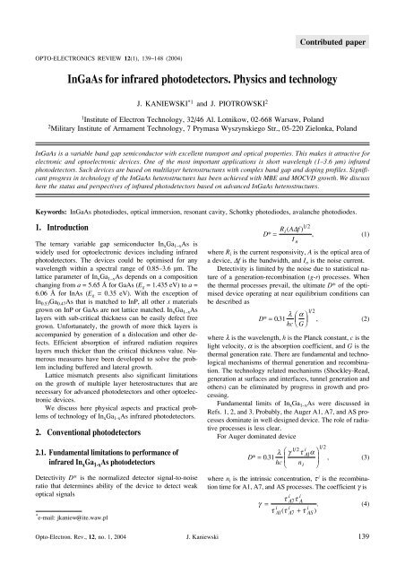
Contributed paperOPTO-ELECTRONICS REVIEW 12(1), 139–148 (2004)<strong>InGaAs</strong> <strong>for</strong> <strong>infrared</strong> <strong>photodetectors</strong>. <strong>Physics</strong> <strong>and</strong> <strong>technology</strong>J. KANIEWSKI *1 <strong>and</strong> J. PIOTROWSKI 21 Institute of Electron Technology, 32/46 Al. Lotnikow, 02-668 Warsaw, Pol<strong>and</strong>2 Military Institute of Armament Technology, 7 Prymasa Wyszynskiego Str., 05-220 Zielonka, Pol<strong>and</strong><strong>InGaAs</strong> is a variable b<strong>and</strong> gap semiconductor with excellent transport <strong>and</strong> optical properties. This makes it attractive <strong>for</strong>electronic <strong>and</strong> optoelectronic devices. One of the most important applications is short wavelengh (1–3.6 µm) <strong>infrared</strong><strong>photodetectors</strong>. Such devices are based on multilayer heterostructures with complex b<strong>and</strong> gap <strong>and</strong> doping profiles. Significantprogress in <strong>technology</strong> of the <strong>InGaAs</strong> heterostructures has been achieved with MBE <strong>and</strong> MOCVD growth. We discusshere the status <strong>and</strong> perspectives of <strong>infrared</strong> <strong>photodetectors</strong> based on advanced <strong>InGaAs</strong> heterostructures.Keywords: <strong>InGaAs</strong> photodiodes, optical immersion, resonant cavity, Schottky photodiodes, avalanche photodiodes.1. IntroductionThe ternary variable gap semiconductor In x Ga 1–x As iswidely used <strong>for</strong> optoelectronic devices including <strong>infrared</strong><strong>photodetectors</strong>. The devices could be optimised <strong>for</strong> anywavelength within a spectral range of 0.85–3.6 µm. Thelattice parameter of In x Ga 1–x As depends on a compositionchanging from a = 5.65 Å <strong>for</strong> GaAs (E g = 1.435 eV) to a =6.06 Å <strong>for</strong> InAs (E g = 0.35 eV). With the exception ofIn 0.53 Ga 0.47 As that is matched to InP, all other x materialsgrown on InP or GaAs are not lattice matched. In x Ga 1–x Aslayers with sub-critical thickness can be easily defect freegrown. Un<strong>for</strong>tunately, the growth of more thick layers isaccompanied by generation of a dislocation <strong>and</strong> other defects.Efficient absorption of <strong>infrared</strong> radiation requireslayers much thicker than the critical thickness value. Numerousmeasures have been developed to solve the problemincluding buffered <strong>and</strong> lateral growth.Lattice mismatch presents also significant limitationson the growth of multiple layer heterostructures that arenecessary <strong>for</strong> advanced <strong>photodetectors</strong> <strong>and</strong> other optoelectronicdevices.We discuss here physical aspects <strong>and</strong> practical problemsof <strong>technology</strong> of In x Ga 1-x As <strong>infrared</strong> <strong>photodetectors</strong>.2. Conventional <strong>photodetectors</strong>2.1. Fundamental limitations to per<strong>for</strong>mance of<strong>infrared</strong> In x Ga 1-x As <strong>photodetectors</strong>Detectivity D* is the normalized detector signal-to-noiseratio that determines ability of the device to detect weakoptical signals* e-mail: jkaniew@ite.waw.plRi( ADf) 12 /D*=, (1)I nwhere R i is the current responsivity, A is the optical area ofa device, Df is the b<strong>and</strong>width, <strong>and</strong> I n is the noise current.Detectivity is limited by the noise due to statistical natureof a generation-recombination (g-r) processes. Whenthe thermal processes prevail, the ultimate D* of the optimiseddevice operating at near equilibrium conditions canbe described asl æaöD* = 031 . ç ÷hc èGø12 /, (2)where l is the wavelength, h is the Planck constant, c is thelight velocity, a is the absorption coefficient, <strong>and</strong> G is thethermal generation rate. There are fundamental <strong>and</strong> technologicalmechanisms of thermal generation <strong>and</strong> recombination.The <strong>technology</strong> related mechanisms (Shockley-Read,generation at surfaces <strong>and</strong> interfaces, tunnel generation <strong>and</strong>others) can be eliminated by progress in growth <strong>and</strong> processing.Fundamental limits of In x Ga 1–x As were discussed inRefs. 1, 2, <strong>and</strong> 3. Probably, the Auger A1, A7, <strong>and</strong> AS processesdominate in well-designed device. The role of radiativeprocesses is less clear.For Auger dominated device12 /l æg t öAD* = .1a031hc çè n ÷i øi12 /, (3)where n i is the intrinsic concentration, t i is the recombinationtime <strong>for</strong> A1, A7, <strong>and</strong> AS processes. The coefficient g isgiiAt A7t=i i it ( t + t ) . (4)A1 A7ASOpto-Electron. Rev., 12, no. 1, 2004 J. Kaniewski 139
<strong>InGaAs</strong> <strong>for</strong> <strong>infrared</strong> <strong>photodetectors</strong>. <strong>Physics</strong> <strong>and</strong> <strong>technology</strong>Fig. 1. Detectivity of In x Ga 1–x As <strong>photodetectors</strong> as a function ofthe wavelength <strong>for</strong> which the detector is optimised.As shows Eq. (3), the ultimate detectivity significantlydepends on the wavelength <strong>for</strong> which the detector is optimised.As calculated, the ultimate detectivity changes from3×10 13 cmHz 1/2 /W <strong>for</strong> l = 2 µm to 3×10 10 cmHz 1/2 /W <strong>for</strong>l = 3.4 µm (Fig. 1).The optimised In x Ga 1–x As <strong>photodetectors</strong> require appropriatedoping of the absorber region (Fig. 2). The doping leveldepends on the wavelength. The donor doping of 3×10 15 cm –3is suitable <strong>for</strong> >3 µm device while » 1×10 14 cm –3 <strong>for</strong>l = 2 µm. So, pure material may be difficult to grow.Fig. 2. Optimised doping level of In x Ga 1–x As absorber as afunction of the wavelength <strong>for</strong> which the detector is optimised.Figure 3 shows an optimised thickness of an absorber.The thickness increases with a wavelength, changing from5.2 µm to 6.7 µm <strong>for</strong> 2 µm <strong>and</strong> 3.4 µm wavelength <strong>for</strong> a singlepass of IR radiation. It should be noted that double passIR devices need absorbers thinner by a half. A thicknessweakly depends on the absorber concentration (Fig. 3).In addition to the absorber region, practical devices requireadditional regions that can sense charge carriersphotogenerated in the absorber. The p + -i-n + structure istypically used <strong>for</strong> a structure <strong>for</strong> In x Ga 1–x As photovoltaicdevice. The per<strong>for</strong>mance of such devices can be affectedFig. 3. Optimised absorber thickness <strong>for</strong> 2 µm (x = 0.82) <strong>and</strong> 3.4 µm(x = 1) devices. Single pass of radiation is assumed.by the additional thermal g-r processes at the p + <strong>and</strong>-n + regions,contacts, interfaces, space charge regions, <strong>and</strong> othernoise sources. The common way to eliminate the detrimentalprocesses is the use of sophisticated multilayerheterojunction device structures.A frequency response of the photovoltaic devices islimited by a transport of the photogenerated charge carriersthrough the absorber region <strong>and</strong> by RC time constant.A transport through the absorber region is a combination ofdiffusion <strong>and</strong> drift. In x Ga 1–x As is the material of choice <strong>for</strong>fast photodiode due to exceptionally large diffusion coefficientof electrons. It should be stressed that the frequencyoptimised In x Ga 1–x As devices require lightly p-type dopedabsorber region <strong>for</strong> electron mobilities, much larger comparedto that of holes.The diffusion transport times at a room temperature areless than >100 ps <strong>for</strong> extrinsic p-type » 5-µm thick InAs absorber.Further reduction can be achieved with the thinnerabsorber. Drift transport in reverse biased devices may reducethe transit time further.The main limitation of response time typically comesfrom the RC time constant. For current mode operation, theRC time constant is determined by the junction capacitance<strong>and</strong> the photodiode series resistance. Reduction of seriesresistance by almost two orders of magnitude is possibleusing the structures with heavily doped n-type material <strong>for</strong>the mesa base, in comparison with p-type base of the samedoping. This results in corresponding reduction of the RCtime constant.A very short RC time constant is expected in opticallyimmersed photodiodes with a very small area of an activeregion. With these improvements, In x Ga 1–x As photodiodescan be used <strong>for</strong> gigahertz range detection of IR radiation.2.2. Optical immersion of <strong>infrared</strong> <strong>photodetectors</strong>An efficient way to reduce the total thermal generation processesis reduction of physical size of the detector in comparisonto its apparent optical size. Typically, this is140 Opto-Electron. Rev., 12, no. 1, 2004 © 2004 COSiW SEP, Warsaw
Contributed paperachieved by optical immersion of the detector to hemi- orhyperhemispherical lens prepared from a high refraction indexmaterial [4–6]. This can be implemented using monolithicoptical immersion where the lens is <strong>for</strong>med in transparentdetector substrate material.Table 1 shows the gains due to use of GaAs immersionlens. This material with a large refraction index is transparentin a wide spectral range of (0.9–20 µm) <strong>and</strong> is frequently usedas a substrate <strong>for</strong> device structures. As we can see, optical immersionsignificantly improves per<strong>for</strong>mance of IR devices.Table 1. Relative gains due to use of optical immersion to GaAslenses.Parameter Hemisphere Hyper-hemisphereLinear size n (»3.4) n 2 (»12)Area n 2 (»12) n 4 (»134)Voltage responsivity n 2 (»12) n 4 (»134)Detectivity n (»3.4) n 2 (»12)Capacitance n 2 (»12) n 4 (»134)Fig. 5. Peltier cooled optically immersed In(GaAl)Asphotodetector.Figures 4 <strong>and</strong> 5 show GaAs immersion lenses fabricatedat the Vigo System S.A. using a monolithic approach.This <strong>technology</strong> requires relatively thick substrate, in dependenceon a detector size. The lenses are prepared withnumerically controlled mechano-chemical machinning.Small immersion lenses (< 0.5 mm dia) <strong>and</strong> lens arraysare fabricated with photolithography-assisted micromachinning(Figs. 6 <strong>and</strong> 7).2.3. Practical implementation of InAs/GaAsphotovoltaic detectorThe advanced InAs/GaAs <strong>photodetectors</strong> have been implementedby Institute of Electron Technology (ITE) in cooperationwith VIGO SYSTEM S.A. The detector structuresare grown by MBE at ITE while processing <strong>and</strong> lens fabri-Fig. 6. Top view of a fragment of lens array with 50 µm pixel size.Fig. 4. 1-mm dia microlens prepared by mechano-chemicalmachining.Fig. 7. SEM micrograph of 50 µm dia microlens. The lens shapeapproaches to some degree ideal spherical shape.Opto-Electron. Rev., 12, no. 1, 2004 J. Kaniewski 141
Contributed paperFrom Eq. (6), the quantum efficiency at the certain advalue is maximised whenR-2d= R ea . (7)1 2Figure 11 shows the maximum h max as a function of ad<strong>for</strong> various R 2 values. To attain the highest h, near unity R 2is desirable. For conventional detectors, without the cavityeffect (R 2 = 0), quantum efficiency higher than 90% can berealized only <strong>for</strong> a thick (> 2 µm) active layer (curve R 2 =0in Fig. 11). For RCE detector, when R 2 = 0.99, the h > 90%can be obtained <strong>for</strong> < 0.05-µm thick layer (a =10 4 cm –1 ).This fact is very helpful towards improving the high-speedper<strong>for</strong>mance of detectors reducing the electronic transit time.Fig. 12. Optical field distribution in RCE detector as a function ofwavelength <strong>and</strong> position. Top <strong>and</strong> bottom mirrors are 5 <strong>and</strong> 15periods GaAs/AlAs. Cavity is optimised <strong>for</strong> the wavelength of0.9 µm (after Refs. 8 <strong>and</strong> 9).Fig. 10. Wavelength dependence of quantum efficiency <strong>for</strong> RCEdetectors (after Ref. 7).The spatial distribution of the optical field inside thecavity is a specific feature of the cavity. It arises from thest<strong>and</strong>ing wave <strong>for</strong>med by the two propagating waves. Acalculated distribution of the optical field is presented inFig. 12. It follows that h, which is derived from the powerabsorbed in the active region, depends on a position of theactive region in the optical field. In order to obtain maximumvalue of the detector efficiency, the active regionshould be placed in a wave antinode position.The st<strong>and</strong>ing wave effect is conveniently included inthe calculation of as an effective absorption coefficient,i.e., a eff = SWE × a, where SWE is the st<strong>and</strong>ing wave coefficient.The SWE coefficient is an explicit function of thecavity properties [8,9].Earlier, we confined our consideration of h to a normalincidence. The changes of a detector quantum efficiencyversus angle incidence are presented in Fig. 13. The calcu-Fig. 11. Maximum quantum efficiency as a function of normalisedabsorption coefficient (after Ref. 7).Fig. 13. Changes of h <strong>for</strong> off-angle incidence at l = 1.0 µm <strong>and</strong>l = 1.5 µm <strong>and</strong> different finesses F = 10 <strong>and</strong> F = 20 (after Ref. 7).Opto-Electron. Rev., 12, no. 1, 2004 J. Kaniewski 143
<strong>InGaAs</strong> <strong>for</strong> <strong>infrared</strong> <strong>photodetectors</strong>. <strong>Physics</strong> <strong>and</strong> <strong>technology</strong>lations were per<strong>for</strong>med <strong>for</strong> different wavelengths <strong>and</strong> differentvalues of the finesse F (F = FSR/Dl 1/2 , where Dl 1/2is half width of a resonant peak). It indicates that h is themost sensitive to the angle of incidence in the high F cavityat the shorter l <strong>and</strong> quantum efficiency degrades by 20%above 10°. The simulations show that RCE detectors cannotwork well, even with quite slow optics.The per<strong>for</strong>mance of RCE-PD mainly depends on the realizationof a low loss cavity. The mirrors <strong>and</strong> cavity materialmust be non-absorbing at the detection wavelength <strong>and</strong>the mirrors must have high reflectivity. Generally, mirrorscan be fabricated as metallic, dielectric, DBR (distributedBragg reflectors made of semiconducting or dielectric layers)or hybride (DBR + metal).The active layer material must have a smaller b<strong>and</strong>gapmaterial than the mirror <strong>and</strong> cavity materials but it shouldnot be so small that large heterojunction b<strong>and</strong> offsets hinderthe extraction of photogenerated carriers. The activelayer absorption coefficient should be moderate, i.e.,10 3 –10 4 cm –1 <strong>for</strong> the operation wavelength.Different material combinations satisfy all of the aboverequirements. The <strong>InGaAs</strong> material system <strong>for</strong> RCE detectionis used in two combinations of semiconductors,AlGaAs/GaAs/<strong>InGaAs</strong> <strong>and</strong> InP/<strong>InGaAs</strong>/InAlAs.Application of <strong>InGaAs</strong> as the active material allows <strong>for</strong>extension device operation spectrum to the wavelength longerthan 900 nm. This ternary compound containing smallamount of In can be grown on GaAs substrate. In this caseAlAs <strong>and</strong> GaAs, having good refractive index contrast, canbe used <strong>for</strong> construction of the mirrors of the resonant cavitywith nearly unit reflectivity with about twenty periodquarter wave superlattice.In x Ga 1–x As containing higher amount of indium (x »0.5) is usually grown on InP substrate. In 0.53 Ga 0.47 As <strong>and</strong>In 0.52 Al 0.48 As lattice matched to InP have rather poor refractiveindex contrast <strong>and</strong> increased number of periods(» 35) are required to achieve nearly unit reflectivity of themirror. For the detectors operating at 1.3–1.55 µm wavelengthrange, quaternary compounds like InGaAlAs <strong>and</strong><strong>InGaAs</strong>P lattice matched to InP are more suitable <strong>for</strong> mirror<strong>for</strong>mation.3.2. Practical implementation of RCE-PDsTo the date, <strong>InGaAs</strong> ternary compound has been the mostcommonly studied ternary compound <strong>for</strong> RCE detectionbecause of the easiness with which GaAs <strong>and</strong> InP basedheterostructures can be grown by molecular beam epitaxy(MBE) <strong>and</strong> metalorganic chemical vapour deposition(MOCVD) [10]. The capabilities have been demonstratedin many practical <strong>photodetectors</strong>.3.2.1. RCE-Schottky <strong>photodetectors</strong>The AlGaAs/GaAs/<strong>InGaAs</strong> based RCE-Schottkyphotodetector, presented in Ref. 11, operated at 895 nm.Fig. 14. Schematic cross-section of the RCE Schottky photodiode(after Ref. 11).A schematic representation of this structure is shown inFig. 14. The device structure was grown on a GaAs substrateby MBE. The cavity is <strong>for</strong>med by 15 pairsAlAs/GaAs DBR bottom reflector <strong>and</strong> a semi transparentAu contact on the top. The <strong>InGaAs</strong> absorption layer has anIn mole fraction less than 10% <strong>and</strong> both heterojunctions arelinearly graded <strong>for</strong> 25 nm to avoid carrier trapping. The positionof the absorption layer in the depletion region is optimisedto yield minimum transit time <strong>for</strong> electrons <strong>and</strong> holes[11]. The device was fabricated with mesa isolation. To reducethe parasitic capacitance of the photodetector, theSchottky metal was connected to the contact pads with anAu air-bridge. A 200 nm Si 3 N 4 coating on the top wasused.The optimised RCE-Schottky photodiode has a 3 dBb<strong>and</strong>width of »100 GHz <strong>and</strong> b<strong>and</strong>width-efficiency product> 70 GHz.Using the indium tin oxide (ITO) <strong>for</strong> the Schottky diodesolves the problems of optical losses <strong>and</strong> scattering causedby the Schottky metal. For the RCE-ITO-Schottky diodefabricated by Biyikli et al. with an area of 5×5 µm, theb<strong>and</strong>width was 60 GHz while the quantum efficiency was75% <strong>for</strong> a reverse voltage of 4 V [12]. This results in ab<strong>and</strong>width-efficiency product of 45 GHz.3.2.2. RCE avalanche PDThe internal gain of avalanche photodiodes (APDs) providessubstantial improvement in signal-to-noise characteristicscompared to other types of PDs. The APD structurethat has been widely deployed is the separate absorption<strong>and</strong> multiplication region (SAM) APD. It consists of awide-b<strong>and</strong>gap multiplication region <strong>and</strong> a narrow-b<strong>and</strong>gapabsorbing layer separated by a transition region that reducesthe accumulation of a charge at the interface betweenthe multiplication <strong>and</strong> absorption regions which improvesthe low-gain b<strong>and</strong>width.In order to reduce the transit time <strong>and</strong> thus improve thefrequency response at low gains, the APD layers are incorporatedinto a resonant-cavity structure [13,14]. The device144 Opto-Electron. Rev., 12, no. 1, 2004 © 2004 COSiW SEP, Warsaw
Contributed paperFig. 15. Schematic cross-section of <strong>InGaAs</strong>-InAlAs SAM APD device (after Ref. 14).structure is shown in Fig. 15. Starting from a semi-insulatingInP substrate, the bottom mirror, which consistedof 30 l/4 pairs of n + -In 0.53 Ga 0.47 As/In 0.52 Al 0.48 As, wasgrown by MBE. After the growth of the thin undopedIn 0.52 Al 0.48 As multiplication region, a p-type In 0.52 Al 0.48 Ascharge layer was inserted to ensure that the electric field inthe adjacent absorption region would be < 1×10 5 V/cm.This was followed by the 60 nm-thick In 0.53 Ga 0.47 As absorptionlayer. Finally, an undoped In 0.52 Al 0.48 As spacer<strong>and</strong> a p + -In 0.52 Al 0.48 As top layer were grown. To fabricate ahigh-speed device, first a Ti-Pt-Au contact metal ring wasdeposited <strong>and</strong> a mesa with the diameter of 14 µm was<strong>for</strong>med by chemical etching.Due to the resonant-cavity scheme, these APDs operatingat 1.55 µm exhibited high external quantum efficiency70% <strong>and</strong> a high unity-gain b<strong>and</strong>width of 24 GHz. Utilizingthe excellent noise characteristics of a thin InAlAs multiplicationregion, a record value of a gain-b<strong>and</strong>width productof 290 GHz was achieved.layer as the active medium. The thickness of the spacer layerswere chosen so that the three absorbing layers are locatedat the antinodes of the st<strong>and</strong>ing wave optical field inthe cavity [Fig. 16(b)]. The investigated devices, shownschematically in Fig. 17(a), were grown by MBE onn + -GaAs substrate. Thirteen period AlAs/GaAs quarter-wavestacks <strong>for</strong>med bottom mirror with the reflectivityabout 90% at the centre wavelength 900 nm. The threeIn 0.05 Ga 0.95 As active layers with each layer of the thickness40 nm were s<strong>and</strong>witched between GaAs layers. The topmirror with 30% reflectivity was <strong>for</strong>med by air <strong>and</strong> semiconductorinterface.The peak quantum efficiency of the triple-layer resonant--periodic-absorber photodiode was 65% [see Fig. 17(b)]. An enhancementof 30% has been achieved by a periodic absorberstructure as compared to a st<strong>and</strong>ard RCE photodiode with asingle absorbing layer of the same total thickness.3.2.3. RCE p-i-n PDThe first RCE p-i-n was reported by Dentai et al. who studiedan <strong>InGaAs</strong>/<strong>InGaAs</strong>P/InP structure designed to operatenear 1.55 µm [15]. A quantum efficiency of 82% wasachieved using a 200 <strong>InGaAs</strong> absorbing layer with R 1 =0.7 <strong>and</strong> R 2 = 0.95.RCE p-i-n PDs with a periodic absorber structure weredemonstrated by Huang et al. to detect 870-nm wavelength[16]. Figure 16(a) depicts the schematic structure of a typicalRC photodiode with a single absorbing layer placed in awave antinode position. In order to improve quantum efficiencyof RCE p-i-n PD, it was proposed to use a tripleFig. 16. Schematic structures of RCE PD with a single absorbinglayer (a) <strong>and</strong> resonant-periodic-absorber RCE PD with triple layersas the absorbing medium (b) (after Ref. 16).Opto-Electron. Rev., 12, no. 1, 2004 J. Kaniewski 145
<strong>InGaAs</strong> <strong>for</strong> <strong>infrared</strong> <strong>photodetectors</strong>. <strong>Physics</strong> <strong>and</strong> <strong>technology</strong>Fig. 17. Schematic structure of <strong>InGaAs</strong> resonant-periodic-absorber RCE PD (a), quantum efficiency of the structure (b) (after Ref. 16).In order to simplify <strong>InGaAs</strong>/InP RCE p-i-n PD structuredifferent types of reflectors can be used. Schematic structureof the RCE device utilizing hybrid reflector <strong>and</strong> semiconductingDBR is presented in Table 2.The device is illuminated from the bottom. A detector isgrown on SI-InP substrate. The bottom DBR is made ofIn 0.52 Al 0.48 As <strong>and</strong> In 0.53 Ga 0.32 Al 0.15 As alternative layers.The resonant cavity is <strong>for</strong>med by 78 nm thickIn 0.53 Ga 0.47 As absorption layer, two In 0.52 Al 0.48 As spacerlayers together with two contact In 0.52 Al 0.48 As layers. Topmirror consists of the dielectric DBR <strong>and</strong> Al layer. The detectorstructure was optimised using transfer matrixmethod. The calculations were per<strong>for</strong>med <strong>for</strong> the devicestructure operating at l = 1548 nm. The changes of absorptionof 78-nm thick active layer versus amount ofIn 0.52 Al 0.48 As/In 0.53 Ga 0.32 Al 0.15 As pairs (bottom reflector)<strong>and</strong> Si 3 N 4 /SiO 2 pairs in top reflector are presented in Fig.18. It has been found that more than 90% absorption of theactive layer is obtained when 9 pairs in bottom reflector<strong>and</strong> 3 pairs in top reflector are used (Fig. 19).This result is very important, because relatively smallnumber of pairs is required <strong>for</strong> mirror <strong>for</strong>mation. Additionally,very thin active layer results in subpicosecondtransit time of the RCE p-i-n PD. High quantum efficiency<strong>for</strong> a narrow absorption line centred at 1548 nm can be obtained.The structure can be easily fabricated by MBE.Fig. 18. Absorption of 78 nm thick In 0.53 Ga 0.47 As active layer of RCE p-i-n PD <strong>for</strong> different numbers of pairs of layers in bottom <strong>and</strong> topreflectors.146 Opto-Electron. Rev., 12, no. 1, 2004 © 2004 COSiW SEP, Warsaw
Contributed paperTable 2. Structure of <strong>InGaAs</strong> RCE p-i-n PD grown onto InP.HybridMetallic layer Alreflector-topDielectric DBR Si 3 N 4 /SiO 2Cavity Contact layer p + In 0.52 Al 0.48 AsSemiconductingreflector-bottom4. ConclusionsSpacer layerAbsorption layerSpacer layerContact layerDBR -bottomSubstrateAntireflectioncoatingn – In 0.52 Al 0.48 Asn – In 0.53 Ga 0.47 Asn – In 0.52 Al 0.48 Asn + In 0.52 Al 0.48 AsIn 0.52 Al 0.48 As/In 0.53 Ga 0.32 Al 0.15 AsSI-InPSi 3 N 4<strong>InGaAs</strong> ternary compound is widely used <strong>for</strong> detection ofshort wavelenth <strong>infrared</strong> radiation. Modern <strong>InGaAs</strong> detectorsare fabricated by means of MBE <strong>and</strong> MOCVD technologies<strong>and</strong> advanced processing. It allows <strong>for</strong> production of discretephotodiodes, arrays, as well as optical integrated devices.Conventional detectors can operate at a wide spectralrange whereas RCE PDs are capable to detect narrow resonantwavelength only. The increased optical field allowsRCE PD to be thinner <strong>and</strong> there<strong>for</strong>e faster than conventionalone. RCE PDs exhibit high b<strong>and</strong>width <strong>and</strong> high externalquantum efficiency as well.The refractive microlenses can be used as optical concentrators<strong>for</strong> conventional <strong>photodetectors</strong>. They allow <strong>for</strong>Fig. 19. Spectral dependence of: absorption A total – dotted line,reflection R total – solid line, <strong>and</strong> transmission T total – dashed line,78 nm thick In 0.53 Ga 0.47 As active layer of optimised RCE p-i-nPD.improvement in per<strong>for</strong>mance <strong>and</strong> speed of response of devices.In the case of RCE PDs, strong degradation of quantumefficiency <strong>for</strong> off-normal angle incident radiation isobserved.AcknowledgementsThe authors would like to thank Dr Jan Muszalski <strong>for</strong> modelling<strong>and</strong> optimisation of <strong>InGaAs</strong>/InP RCE photodiodes.This work was partially supported by the Polish Committee<strong>for</strong> Scientific Research under grant No. 4 T11B 015 25.References1. J. Piotrowski <strong>and</strong> J. Kaniewski, “Optimisation of <strong>InGaAs</strong><strong>infrared</strong> photovoltaic detectors”, IEE Proc. Optolectron.146, 173–176 (1999).2. J. Piotrowski, J. Kaniewski, <strong>and</strong> K. Reginski, “Modelling<strong>and</strong> optimisation of <strong>InGaAs</strong> <strong>infrared</strong> photovoltaic detectors”,Nucl. Instr. Methods in Phys. Res. A439, 647–650(2000).3. A. Rogalski, “Per<strong>for</strong>mance limitations of <strong>InGaAs</strong> photodiodes”,Proc. SPIE 3725, 260–269 (1999).4. E.L. Dereniak <strong>and</strong> G.D. Boreman, Infrared Detectors <strong>and</strong>Systems, J. Wiley <strong>and</strong> Sons, N.Y., 1996.5. R.C. Jones, “Immersed radiation detectors”, Appl. Optics 5,607–613 (1962).6. J. Kaniewski, Z. Orman, J. Piotrowski, K. Reginski, <strong>and</strong> M.Romanis, “Advanced <strong>InGaAs</strong> detectors on GaAs substrates”,Proc. SPIE 4130, 749–759 (2000).7. K. Kishino, M.S. Unlu, J. Chyi, J. Reed, L. Arsenault, <strong>and</strong>H. Morkoc, “Resonant cavity-enhanced (RCE) <strong>photodetectors</strong>”,IEEE J. Quantum Electron. 27, 2025–2034 (1991).8. M.S. Unlu <strong>and</strong> S. Strite, “Resonant cavity enhanced photonicdevices”, J. Appl. Phys. 78, 607–639 (1995).9. M.S. Unlu, K. Kishino, H.J. Liaw, <strong>and</strong> H. Morkoc, “A theoreticalstudy of resonant cavity-enhanced <strong>photodetectors</strong>with Ge <strong>and</strong> Si active regions”, J. Appl. Phys. 71,4049–4058 (1992).10. Y.M. El-Batawy <strong>and</strong> M.J. Deen, “Resonant cavity enhanced<strong>photodetectors</strong> (RCE-PDs): structure, material, analysis <strong>and</strong>optimisation”, Proc. SPIE 4999, 363–378 (2003).11. B.M. Onat, M. Gokkavas, E. Ozbay, E.P. Ata, E. Towe <strong>and</strong>M.S. Unlu, “100-GHz resonant cavity enhanced Schottkyphotodiodes”, IEEE Photon. Technol. Lett. 10, 707–709(1998).12. N. Biyikli, I. Kimukin, O. Aytur, M. Gokkavas, M.S. Unlu,<strong>and</strong> E. Ozbay, “45 GHz b<strong>and</strong>with-efficiency resonant-cavityenhanced ITO-Schottky photodiodes”, IEEEPhoton. Technol Lett 13, 705–707 (2001).13. S.S. Martuza, K.A. Anselm, C. Hu, H. Nie, B.G. Streetman,<strong>and</strong> J.C. Campbell, “Resonant cavity enhanced (RCE) separateabsorption <strong>and</strong> multiplication (SAM) avalanchephotodetector (APD)”, IEEE Photon. Technol. Lett. 7,1486–1488 (1995).14. C. Lenox, H. Nie, P. Yuan, G. Kinsey, A.L. Holmes, G.B.Streetman, <strong>and</strong> J.C. Campbell, “Resonant cavity <strong>InGaAs</strong>--InAlAs avalanche photodiodes with gain-b<strong>and</strong>width productof 290 GHz”, IEEE Photon. Technol. Lett. 11,1162–1164 (1999).Opto-Electron. Rev., 12, no. 1, 2004 J. Kaniewski 147
<strong>InGaAs</strong> <strong>for</strong> <strong>infrared</strong> <strong>photodetectors</strong>. <strong>Physics</strong> <strong>and</strong> <strong>technology</strong>15. A.G. Dentai, R. Kuchibhotla, J.C. Campbell, C. Tsai, <strong>and</strong> C.Lei, “High quantum efficiency long-wavelengthInP/<strong>InGaAs</strong> microcavity photodiode”, Electron. Lett 27,2125–2127 (1991).16. F.Y. Huang, A. Salvador, X. Gui, N. Teraguchi, <strong>and</strong> H.Morkoc, “Resonant-cavity GaAs/<strong>InGaAs</strong>/AlAs photodiodeswith a periodic absorber structure”, Appl. Phys. Lett. 63,141–143 (1993).148 Opto-Electron. Rev., 12, no. 1, 2004 © 2004 COSiW SEP, Warsaw