InGaAs for infrared photodetectors. Physics and technology
InGaAs for infrared photodetectors. Physics and technology
InGaAs for infrared photodetectors. Physics and technology

Create successful ePaper yourself
Turn your PDF publications into a flip-book with our unique Google optimized e-Paper software.
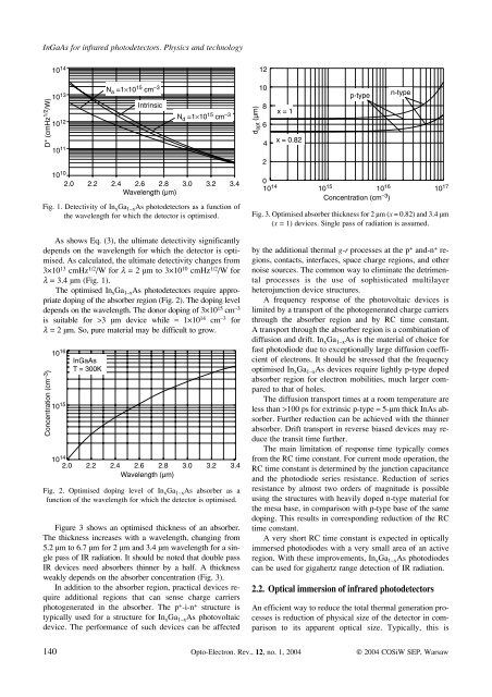
<strong>InGaAs</strong> <strong>for</strong> <strong>infrared</strong> <strong>photodetectors</strong>. <strong>Physics</strong> <strong>and</strong> <strong>technology</strong>Fig. 1. Detectivity of In x Ga 1–x As <strong>photodetectors</strong> as a function ofthe wavelength <strong>for</strong> which the detector is optimised.As shows Eq. (3), the ultimate detectivity significantlydepends on the wavelength <strong>for</strong> which the detector is optimised.As calculated, the ultimate detectivity changes from3×10 13 cmHz 1/2 /W <strong>for</strong> l = 2 µm to 3×10 10 cmHz 1/2 /W <strong>for</strong>l = 3.4 µm (Fig. 1).The optimised In x Ga 1–x As <strong>photodetectors</strong> require appropriatedoping of the absorber region (Fig. 2). The doping leveldepends on the wavelength. The donor doping of 3×10 15 cm –3is suitable <strong>for</strong> >3 µm device while » 1×10 14 cm –3 <strong>for</strong>l = 2 µm. So, pure material may be difficult to grow.Fig. 2. Optimised doping level of In x Ga 1–x As absorber as afunction of the wavelength <strong>for</strong> which the detector is optimised.Figure 3 shows an optimised thickness of an absorber.The thickness increases with a wavelength, changing from5.2 µm to 6.7 µm <strong>for</strong> 2 µm <strong>and</strong> 3.4 µm wavelength <strong>for</strong> a singlepass of IR radiation. It should be noted that double passIR devices need absorbers thinner by a half. A thicknessweakly depends on the absorber concentration (Fig. 3).In addition to the absorber region, practical devices requireadditional regions that can sense charge carriersphotogenerated in the absorber. The p + -i-n + structure istypically used <strong>for</strong> a structure <strong>for</strong> In x Ga 1–x As photovoltaicdevice. The per<strong>for</strong>mance of such devices can be affectedFig. 3. Optimised absorber thickness <strong>for</strong> 2 µm (x = 0.82) <strong>and</strong> 3.4 µm(x = 1) devices. Single pass of radiation is assumed.by the additional thermal g-r processes at the p + <strong>and</strong>-n + regions,contacts, interfaces, space charge regions, <strong>and</strong> othernoise sources. The common way to eliminate the detrimentalprocesses is the use of sophisticated multilayerheterojunction device structures.A frequency response of the photovoltaic devices islimited by a transport of the photogenerated charge carriersthrough the absorber region <strong>and</strong> by RC time constant.A transport through the absorber region is a combination ofdiffusion <strong>and</strong> drift. In x Ga 1–x As is the material of choice <strong>for</strong>fast photodiode due to exceptionally large diffusion coefficientof electrons. It should be stressed that the frequencyoptimised In x Ga 1–x As devices require lightly p-type dopedabsorber region <strong>for</strong> electron mobilities, much larger comparedto that of holes.The diffusion transport times at a room temperature areless than >100 ps <strong>for</strong> extrinsic p-type » 5-µm thick InAs absorber.Further reduction can be achieved with the thinnerabsorber. Drift transport in reverse biased devices may reducethe transit time further.The main limitation of response time typically comesfrom the RC time constant. For current mode operation, theRC time constant is determined by the junction capacitance<strong>and</strong> the photodiode series resistance. Reduction of seriesresistance by almost two orders of magnitude is possibleusing the structures with heavily doped n-type material <strong>for</strong>the mesa base, in comparison with p-type base of the samedoping. This results in corresponding reduction of the RCtime constant.A very short RC time constant is expected in opticallyimmersed photodiodes with a very small area of an activeregion. With these improvements, In x Ga 1–x As photodiodescan be used <strong>for</strong> gigahertz range detection of IR radiation.2.2. Optical immersion of <strong>infrared</strong> <strong>photodetectors</strong>An efficient way to reduce the total thermal generation processesis reduction of physical size of the detector in comparisonto its apparent optical size. Typically, this is140 Opto-Electron. Rev., 12, no. 1, 2004 © 2004 COSiW SEP, Warsaw