<strong>InGaAs</strong> <strong>for</strong> <strong>infrared</strong> <strong>photodetectors</strong>. <strong>Physics</strong> <strong>and</strong> <strong>technology</strong>lations were per<strong>for</strong>med <strong>for</strong> different wavelengths <strong>and</strong> differentvalues of the finesse F (F = FSR/Dl 1/2 , where Dl 1/2is half width of a resonant peak). It indicates that h is themost sensitive to the angle of incidence in the high F cavityat the shorter l <strong>and</strong> quantum efficiency degrades by 20%above 10°. The simulations show that RCE detectors cannotwork well, even with quite slow optics.The per<strong>for</strong>mance of RCE-PD mainly depends on the realizationof a low loss cavity. The mirrors <strong>and</strong> cavity materialmust be non-absorbing at the detection wavelength <strong>and</strong>the mirrors must have high reflectivity. Generally, mirrorscan be fabricated as metallic, dielectric, DBR (distributedBragg reflectors made of semiconducting or dielectric layers)or hybride (DBR + metal).The active layer material must have a smaller b<strong>and</strong>gapmaterial than the mirror <strong>and</strong> cavity materials but it shouldnot be so small that large heterojunction b<strong>and</strong> offsets hinderthe extraction of photogenerated carriers. The activelayer absorption coefficient should be moderate, i.e.,10 3 –10 4 cm –1 <strong>for</strong> the operation wavelength.Different material combinations satisfy all of the aboverequirements. The <strong>InGaAs</strong> material system <strong>for</strong> RCE detectionis used in two combinations of semiconductors,AlGaAs/GaAs/<strong>InGaAs</strong> <strong>and</strong> InP/<strong>InGaAs</strong>/InAlAs.Application of <strong>InGaAs</strong> as the active material allows <strong>for</strong>extension device operation spectrum to the wavelength longerthan 900 nm. This ternary compound containing smallamount of In can be grown on GaAs substrate. In this caseAlAs <strong>and</strong> GaAs, having good refractive index contrast, canbe used <strong>for</strong> construction of the mirrors of the resonant cavitywith nearly unit reflectivity with about twenty periodquarter wave superlattice.In x Ga 1–x As containing higher amount of indium (x »0.5) is usually grown on InP substrate. In 0.53 Ga 0.47 As <strong>and</strong>In 0.52 Al 0.48 As lattice matched to InP have rather poor refractiveindex contrast <strong>and</strong> increased number of periods(» 35) are required to achieve nearly unit reflectivity of themirror. For the detectors operating at 1.3–1.55 µm wavelengthrange, quaternary compounds like InGaAlAs <strong>and</strong><strong>InGaAs</strong>P lattice matched to InP are more suitable <strong>for</strong> mirror<strong>for</strong>mation.3.2. Practical implementation of RCE-PDsTo the date, <strong>InGaAs</strong> ternary compound has been the mostcommonly studied ternary compound <strong>for</strong> RCE detectionbecause of the easiness with which GaAs <strong>and</strong> InP basedheterostructures can be grown by molecular beam epitaxy(MBE) <strong>and</strong> metalorganic chemical vapour deposition(MOCVD) [10]. The capabilities have been demonstratedin many practical <strong>photodetectors</strong>.3.2.1. RCE-Schottky <strong>photodetectors</strong>The AlGaAs/GaAs/<strong>InGaAs</strong> based RCE-Schottkyphotodetector, presented in Ref. 11, operated at 895 nm.Fig. 14. Schematic cross-section of the RCE Schottky photodiode(after Ref. 11).A schematic representation of this structure is shown inFig. 14. The device structure was grown on a GaAs substrateby MBE. The cavity is <strong>for</strong>med by 15 pairsAlAs/GaAs DBR bottom reflector <strong>and</strong> a semi transparentAu contact on the top. The <strong>InGaAs</strong> absorption layer has anIn mole fraction less than 10% <strong>and</strong> both heterojunctions arelinearly graded <strong>for</strong> 25 nm to avoid carrier trapping. The positionof the absorption layer in the depletion region is optimisedto yield minimum transit time <strong>for</strong> electrons <strong>and</strong> holes[11]. The device was fabricated with mesa isolation. To reducethe parasitic capacitance of the photodetector, theSchottky metal was connected to the contact pads with anAu air-bridge. A 200 nm Si 3 N 4 coating on the top wasused.The optimised RCE-Schottky photodiode has a 3 dBb<strong>and</strong>width of »100 GHz <strong>and</strong> b<strong>and</strong>width-efficiency product> 70 GHz.Using the indium tin oxide (ITO) <strong>for</strong> the Schottky diodesolves the problems of optical losses <strong>and</strong> scattering causedby the Schottky metal. For the RCE-ITO-Schottky diodefabricated by Biyikli et al. with an area of 5×5 µm, theb<strong>and</strong>width was 60 GHz while the quantum efficiency was75% <strong>for</strong> a reverse voltage of 4 V [12]. This results in ab<strong>and</strong>width-efficiency product of 45 GHz.3.2.2. RCE avalanche PDThe internal gain of avalanche photodiodes (APDs) providessubstantial improvement in signal-to-noise characteristicscompared to other types of PDs. The APD structurethat has been widely deployed is the separate absorption<strong>and</strong> multiplication region (SAM) APD. It consists of awide-b<strong>and</strong>gap multiplication region <strong>and</strong> a narrow-b<strong>and</strong>gapabsorbing layer separated by a transition region that reducesthe accumulation of a charge at the interface betweenthe multiplication <strong>and</strong> absorption regions which improvesthe low-gain b<strong>and</strong>width.In order to reduce the transit time <strong>and</strong> thus improve thefrequency response at low gains, the APD layers are incorporatedinto a resonant-cavity structure [13,14]. The device144 Opto-Electron. Rev., 12, no. 1, 2004 © 2004 COSiW SEP, Warsaw
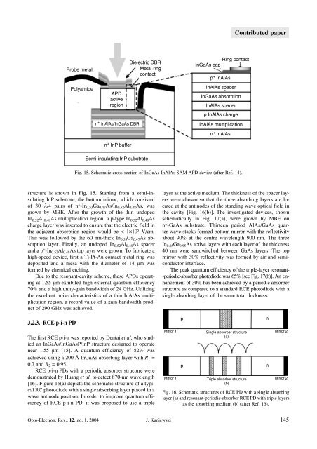
Contributed paperFig. 15. Schematic cross-section of <strong>InGaAs</strong>-InAlAs SAM APD device (after Ref. 14).structure is shown in Fig. 15. Starting from a semi-insulatingInP substrate, the bottom mirror, which consistedof 30 l/4 pairs of n + -In 0.53 Ga 0.47 As/In 0.52 Al 0.48 As, wasgrown by MBE. After the growth of the thin undopedIn 0.52 Al 0.48 As multiplication region, a p-type In 0.52 Al 0.48 Ascharge layer was inserted to ensure that the electric field inthe adjacent absorption region would be < 1×10 5 V/cm.This was followed by the 60 nm-thick In 0.53 Ga 0.47 As absorptionlayer. Finally, an undoped In 0.52 Al 0.48 As spacer<strong>and</strong> a p + -In 0.52 Al 0.48 As top layer were grown. To fabricate ahigh-speed device, first a Ti-Pt-Au contact metal ring wasdeposited <strong>and</strong> a mesa with the diameter of 14 µm was<strong>for</strong>med by chemical etching.Due to the resonant-cavity scheme, these APDs operatingat 1.55 µm exhibited high external quantum efficiency70% <strong>and</strong> a high unity-gain b<strong>and</strong>width of 24 GHz. Utilizingthe excellent noise characteristics of a thin InAlAs multiplicationregion, a record value of a gain-b<strong>and</strong>width productof 290 GHz was achieved.layer as the active medium. The thickness of the spacer layerswere chosen so that the three absorbing layers are locatedat the antinodes of the st<strong>and</strong>ing wave optical field inthe cavity [Fig. 16(b)]. The investigated devices, shownschematically in Fig. 17(a), were grown by MBE onn + -GaAs substrate. Thirteen period AlAs/GaAs quarter-wavestacks <strong>for</strong>med bottom mirror with the reflectivityabout 90% at the centre wavelength 900 nm. The threeIn 0.05 Ga 0.95 As active layers with each layer of the thickness40 nm were s<strong>and</strong>witched between GaAs layers. The topmirror with 30% reflectivity was <strong>for</strong>med by air <strong>and</strong> semiconductorinterface.The peak quantum efficiency of the triple-layer resonant--periodic-absorber photodiode was 65% [see Fig. 17(b)]. An enhancementof 30% has been achieved by a periodic absorberstructure as compared to a st<strong>and</strong>ard RCE photodiode with asingle absorbing layer of the same total thickness.3.2.3. RCE p-i-n PDThe first RCE p-i-n was reported by Dentai et al. who studiedan <strong>InGaAs</strong>/<strong>InGaAs</strong>P/InP structure designed to operatenear 1.55 µm [15]. A quantum efficiency of 82% wasachieved using a 200 <strong>InGaAs</strong> absorbing layer with R 1 =0.7 <strong>and</strong> R 2 = 0.95.RCE p-i-n PDs with a periodic absorber structure weredemonstrated by Huang et al. to detect 870-nm wavelength[16]. Figure 16(a) depicts the schematic structure of a typicalRC photodiode with a single absorbing layer placed in awave antinode position. In order to improve quantum efficiencyof RCE p-i-n PD, it was proposed to use a tripleFig. 16. Schematic structures of RCE PD with a single absorbinglayer (a) <strong>and</strong> resonant-periodic-absorber RCE PD with triple layersas the absorbing medium (b) (after Ref. 16).Opto-Electron. Rev., 12, no. 1, 2004 J. Kaniewski 145