261.PDF file, full text
261.PDF file, full text
261.PDF file, full text

Create successful ePaper yourself
Turn your PDF publications into a flip-book with our unique Google optimized e-Paper software.
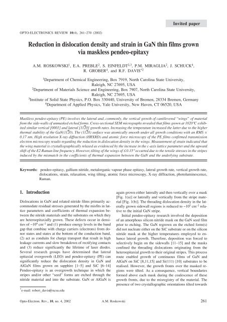
Invited paperOPTO-ELECTRONICS REVIEW 10(4), 261–270 (2002)Reduction in dislocation density and strain in GaN thin films grownvia maskless pendeo-epitaxyA.M. ROSKOWSKI 1 , E.A. PREBLE 2 , S. EINFELDT 2,3 , P.M. MIRAGLIA 2 , J. SCHUCK 4 ,R. GROBER 4 , and R.F. DAVIS *21 Department of Chemical Engineering, Box 7919, North Carolina State University,Raleigh, NC 27695, USA2 Department of Materials Science and Engineering, Box 7907, North Carolina State University,Raleigh, NC 27695, USA3 Institute of Solid State Physics, P.O. Box 330440, University of Bremen, 28334 Bremen, Germany4 Department of Applied Physics, Yale University, New Haven, CT 06520, USAMaskless pendeo-epitaxy (PE) involves the lateral and, commonly, the vertical growth of cantilevered “wings” of materialfrom the side-walls of unmasked etched forms. Cross-sectional SEM micrographs revealed that films grown at 1020°C exhibitedsimilar vertical [0001] and lateral [1120] growth rates. Increasing the temperature increased the latter due to the higherthermal stability of the GaN(1120). The (1120) surface was atomically smooth under all growth conditions with an RMS =0.17 nm. High resolution X-ray diffraction (HRXRD) and atomic force microscopy of the PE films confirmed transmissionelectron microscopy results regarding the reduction in dislocation density in the wings. Measurement of strain indicated thatthe wing material is crystallographically relaxed as evidenced by the increase in the c-axis lattice parameter and the upwardshift of the E2 Raman line frequency. However, tilting of the wings of £ 0.15° occurred due to the tensile stresses in the stripesinduced by the mismatch in the coefficients of thermal expansion between the GaN and the underlying substrate.Keywords:pendeo-epitaxy, gallium nitride, metalorganic vapour phase epitaxy, lateral growth rate, vertical growth rate,dislocations, strain, relaxation, wing tilting, atomic force microscopy, X-ray diffraction, photoluminescence,Raman.1. IntroductionDislocations in GaN and related nitride films primarily accommodateresidual stresses generated by the misfits in latticeparameters and coefficients of thermal expansion betweenthe nitride materials and the substrates on which theyare heteroepitaxially grown. These defects occur in densitiesof ~10 9 cm –2 and (1) produce energy levels in the bandgap that combine with charge carriers (electrons) from donorstates and states at the bottom of the conduction band,(2) act as conduits for charge transport that result in highleakage currents and slow breakdown of rectifying contactsand (3) reduce significantly the lifetime of laser diodes.Several research groups have determined that lateralepitaxial overgrowth (LEO) and pendeo-epitaxy (PE) cansignificantly reduce the dislocation density in GaN andAlGaN films grown on sapphire [1–5] and SiC [6–14]Pendeo-epitaxy is an overgrowth technique in which thestripes and/or other “seed” forms are etched through thenitride material and into the substrate. GaN or AlGaN is* e-mail: robert_davis@ncsu.eduagain grown either laterally and then vertically over a mask[Fig. 1(a)] or laterally and vertically from the stripe material[Fig. 1(b)]. The threading dislocation density in the laterallygrown sidewall regions is reduced to ~10 5 cm –2 relativeto the initial GaN stripe.Initial pendeo-epitaxy research involved the depositionof an amorphous silicon nitride mask on the GaN seed filmprior to etching. The GaN regrown on the etched form(s)did not nucleate either on the SiC substrate or on the siliconnitride mask at the higher temperatures employed to enhancelateral growth. Therefore, deposition was forced toselectively begin on the sidewalls [11–15] and the masksconfined the threading dislocations originating from theheteroepitaxial growth to their original stripes. This processroute enabled growth of continuous films of GaN andAlGaN on SiC [8,11,15] and Si(111) [10] substrates to berealised. However, the growth fronts over the masked regionswere tilted. As a consequence, vertical boundariesformed above each mask during the coalescence of thesegrowth fronts, due to the misregistry of the material. Thepresence of two crystallographic orientations tilted towardsOpto-Electron. Rev., 10, no. 4, 2002 A.M. Roskowski 261
Reduction in dislocation density and strain in GaN thin films grown via maskless pendeo-epitaxyFig. 1. Schematic of: (a) PE growth from GaN seed laterally off the sidewalls then vertically and laterally over the silicon nitride mask;(b) PE growth from GaN seed laterally off the sidewalls and vertically off the stripe.each other has also been reported in GaN films grown viaLEO [4,16–18].Recent research efforts have centred on PE growthwithout the use of a silicon nitride mask, termed “maskless”PE. Lateral and vertical growth is initiated from theGaN stripe, as depicted in Fig. 1(b). The elimination of agrowth mask has several advantages: the crystallographictilt described above that occurs in the overgrown materialis significantly reduced, a source for impurities in the overgrowthmaterial is eliminated and PE growth of AlGaNfilms can be realised. Although AlGaN nucleates on theSiC substrate, sufficiently deep trenches are made to preventcontact between the material growing vertically fromthe bottom of the trench and the material growing laterallyfrom the sidewalls of the stripes [10].In essence, PE is a new approach to selective epitaxy ofGaN and AlGaN layers that incorporates mechanisms ofgrowth exploited by the conventional LEO process, butusually alleviates the mask alignment problems through theuse of the substrate itself as a pseudo-mask. The followingSections describe the recent advancements concerning theeffect of growth parameters on growth rates, surfacemicrostructure, the reduction in defects and strain, and thestructural and optical characteristics of maskless GaN thinfilms grown via PE.2. ExperimentalEach AlN buffer layer, GaN seed layer and maskless PEGaN and/or AlGaN layer was sequentially grown on a6H-SiC(0001) substrate in a cold-walled, vertical, pan-Fig. 2. Composite of cross-sectional TEM micrographs of a PE Al 0.1 Ga 0.9 N film. Note the threading dislocations continue from the GaNstripes into the film.262 Opto-Electron. Rev., 10, no. 4, 2002 © 2002 COSiW SEP, Warsaw
cake-style metalorganic vapour phase epitaxy (MOVPE)system. The 100-nm thick AlN buffer layers and the 1-µmthick GaN seed layers were grown at 20 Torr and plattertemperatures of 1120°C and 1020°C, respectively. The precursorspecies (mass flow rates) of tri-methylaluminum(TMA; 5.4 µmol/min), tri-ethylgallium (TEG; 101 µmol/min) and ammonia (NH 3 ; 0.14 mol/min) were mixed with ahigh-purity H 2 diluent (3 slm) in a two-inch internal diametersleeve located two inches above the substrate.A Ni layer was deposited on patterned photoresiststripes on each GaN seed layer by e-beam evaporation.Etch mask stripes were subsequently produced using standardphotolithography lift-off techniques. An inductivelycoupled plasma (ICP) system and a mixture of Cl 2 andBCl 3 gases were used to etch the unmasked striped regionsthrough the GaN and the AlN and into the near-surface areasof the SiC substrate. The Ni was then removed using a5-min dip in HNO 3 . The remaining GaN seed layer consistedof 2 and 3 µm wide stripes separated by distances of12 and 7 µm, respectively, and oriented along [1120]. Theexposed (1120) sidewalls and the top (0001) face of thestripes were subsequently dipped in 50% hot HCl to cleanthe surface prior to regrowth of the PE layer.The lateral and vertical growth rates of the PE GaNfilms are very sensitive to temperature and the NH 3 /TEG(V/III) molar flow rate ratios. As such, the growth of thesefilms was investigated over the ranges of temperature andTEG flow rates of 1040°C–1100°C and 17–100 µmole/min,respectively. The flow rates of the NH 3 and the H 2 diluentwere maintained at 0.14 mol/min and 3 slm, respectively.The total gas flow into the reactor remained constant for allthe experiments to assure a uniform laminar flow over thesubstrate.Cross-sectional images of the surface microstructure ofthe wing and stripe material were obtained using scanningelectron microscopy (SEM) and were used to calculate thelateral and/or vertical growth rates of these features.Atomic force microscopy (AFM) was employed in the tappingmode to obtain higher resolution micrographs of thegrowth surface as well as the aerial distribution of dislocationsthat terminated at the (0001) surface. Defect characterisationand measurements of the strain via changes inlattice parameter were conducted using the results from onandoff-axis rocking curves and reciprocal space mappingacquired via high-resolution x-ray diffraction (HRXRD).Optical characterisation of spatially resolved (»400 nm)band-edge emission was performed via micro-photoluminescence(PL) at 10 K using a He-Cd (l = 325 nm) laser.Shifts in the frequency of the E2 line measured at 10 K usingan Ar-ion (l = 488 nm) laser coupled to micro-Ramanunit with a spatial resolution of »700 nm, revealed discreteregions of strain in the PE films. Micro-Raman spectra ofthe LO phonon also yielded information regarding the carrierconcentration of the overgrown material. Secondary-ionmass spectroscopy (SIMS) depth pro<strong>file</strong>s were obtainedto determine the presence and concentrations of carbon,oxygen and silicon in the GaN films.3. Results and discussionInvited paper3.1. Pendeo-epitaxial growth and decomposition onGaN(0001) and (1120) surfacesHigh lateral growth rates are desired in both LEO and PEtechniques to achieve rapid coalescence and commerciallyviability. Reported factors that increase the lateral growthrate of GaN films in the [1120] direction from [1100] orientedstripes include growth temperature [12,19], V/III molarflow rate ratio [1,2] and modulation of the NH 3 flowrate [5,9].Figures 3 and 4 are related by the lower case letters ineach and show analytically and pictorially, respectively,the effect of growth temperature for two V/III flow rate ratioson the lateral/vertical GaN growth rate ratios (R). TheV/III ratio was increased from 1323 to 6160 at all temperaturesvia reduction in the TEG flow rate from 101.2µmol/min to 16.7 µmol/min. The most dramatic increase inR occurred for the V/III ratio of 6160 after the growth temperaturewas increased beyond 1060°C, as shown, e.g., inFig. 3(d) and the associated Fig. 4(d). However, the roughnessof the (0001) surface also increased above an R = 10;as seen in the SEM image, Fig. 4(d), of a sample having avalue of R of approximately 24. Additional understandingregarding the changes in the values of R can be obtained byuncoupling the lateral and vertical growth rates and plottingthem as a function of temperature in the manner shownin Fig. 5. Calculation of the growth rates from the SEMcross-sectional micrographs shown in Fig. 4 and additionalmicrographs acquired for the PE GaN films grown at theintermediate temperatures revealed that the lateral growthrate increased with increasing temperature and the verticalgrowth rate either remained constant or decreased for bothV/III ratios. In Fig. 5, the growth rates, both laterally andvertically, are greater for the V/III ratios of 1323 than forthe ratio of 6160 due to the larger amount of TEG used inFig. 3. Ratio of lateral (L)-to-vertical (V) growth rates (R) as afunction of growth temperature and V(NH 3 )/III(TEG) ratio. TheNH 3 flow rate remained constant. Inset shows how a representativevalue of R was calculated for these films. The growth time was 1 hrfor each point.Opto-Electron. Rev., 10, no. 4, 2002 A.M. Roskowski 263
Reduction in dislocation density and strain in GaN thin films grown via maskless pendeo-epitaxyFig. 4. Cross-sectional SEM [1100] view of uncoalesced PE GaN films grown under different temperatures and V/III gas ratios for 1 hourat 20 torr total pressure. The original GaN seed was 1 µm tall. Note: the magnification for each SEM picture is different.growth. For V/III ratios of 1323, the vertical growth wasdominant over lateral growth at temperatures below»1080°C. An increase in lateral growth at 1100°C changedthe value of R to greater than 1. The dramatic increase inthe value of R above 1 for PE growth at a V/III ratio =6160 for T > 1060°C occurred due to the drop in the verticalgrowth rate to near zero. At 1060°C and above, decompositionof the (0001) surface occurred in competition withthe vertical growth of GaN; however, it did not affect lateralgrowth. This competition is obvious in Fig. 4(d) whereFig. 5. Lateral and vertical growth rates as a function of growthtemperature and V(NH 3 )/III(TEG) ratio. The NH 3 flow rateremained constant.growth in the [1120] has produced large wings off the originalseed, but the (0001) surface is rough and very littlevertical growth has occurred.Gallium nitride, despite strong chemical bonding decomposesabove 800°C in flowing hydrogen [20], andMOVPE becomes a near equilibrium competitive processbetween adatom incorporation, desorption into the gasphase and GaN decomposition. This competition was particularlyrelevant and made complex in the present research,as the PE GaN films were grown at temperaturesexceeding those normally employed in the MOVPE of thiscompound in the presence of both H 2 and NH 3 . This lattergas decomposes to provide atomic nitrogen as well asatomic and additional molecular hydrogen that chemicallyreact with the GaN(0001) surface. An overview of prior researchregarding GaN decomposition in H 2 and/or NH 3with and without the presence of TEG is given below.The decomposition of the GaN(0001) surface has beenmeasured by gravimetric means in H 2 [21–23] and NH 3[24,25] for pressure ranges of 10–700 torr, which encompassesthe range used most commonly in the MOCVD ofthis material. Rebey et al. [21] reported that the decompositionrate at 1050°C increased rapidly with increasing H 2flow rate and at 3 slm reached 30 µm/hr. They measured acritical temperature of 830°C, at which the rate-limiting decompositionprocess changed from surface kinetics(E a ~1.87 eV) to diffusion in the boundary layer(E a ~0.38 eV). They postulated the decomposition sequencefor GaN to be (a) the desorption of surface nitrogen264 Opto-Electron. Rev., 10, no. 4, 2002 © 2002 COSiW SEP, Warsaw
Invited paperFig. 6. AFM micrographs acquired from: (a) the (0001) GaN stripe area; (b) the wing GaN (0001) area; (c) the GaN (1120) wing face.Arrows in (a) and (c) point to intersections of dislocations at the surface of these respective planes. The striations in (c) are electronic noisefrom the AFM; step structures have never been observed on this plane.atoms leading to a Ga-rich surface, (b) the diffusion of bulknitrogen atoms to the surface, (c) the subsequent formationand desorption of nitrogen molecules, and (d) the formationof Ga droplets.The results of further studies show that decompositionrates of the GaN(0001) surface at 1000°C inH 2 are reducedtwo orders of magnitude by the addition of NH 3 asit blocks sites needed for GaN decomposition [23]. Forthis reason a large NH 3 /TEG ratio is used during MOVPEgrowth. Nitrogen generated from the decomposition ofNH 3 must be larger than the desorption flux of N to guaranteea saturation surface coverage of this species [26]. Iftoo much NH 3 is used the number of open surface sites isreduced and the growth rate decreases [27,28]. However,there is a range of NH 3 flow rates wherein the growthrates are controlled by the flux of metal species to the surfaceof the growing film. This is demonstrated in Fig. 5 bythe reduction in vertical growth of the PE samples at alltemperatures with a reduction in TEG flow (increase inV/III ratio).As the growth temperature increases, it is postulatedthat the role of NH 3 gradually changes from that of asite-blocker to that which provides atomic surface hydrogenvia decomposition. This hydrogen reacts with atomicsurface nitrogen to form volatile species and consequentdecomposition of the GaN. To check this hypothesis thatdecomposition of GaN(0001) is enhanced under conditionsof large NH 3 flow rates, a PE growth run was conducted at1100°C wherein the TEG flowrate was held constant at21.7 µmol/min and the NH 3 flow rate increased from 3 slmto 5 slm. Increasing decomposition was manifest in the increasingroughness of the (0001) surface as well as a lowvertical growth rate.Early experiments of GaN growth on different crystallographicorientations of sapphire crystals also showedthat (1120) has a higher thermal stability than (0001) [29].This was also borne out in our PE GaN experiments at1100°C where in growth occurred along [1120] andgrowth and decomposition occurred concomitantly along[0001]. Moreover, no indication of (1120) decompositionwas observed under any growth conditions at 1100°C includinglow TEG and high NH 3 flow rates. As such, lateralgrowth rates along [1120] can be controlled solely bytemperature.3.2. Surface microscopy and defectsThe GaN(0001) surface is a Ga-terminated polar surfaceand much is known about growth and decomposition kineticson this surface, as described above. Growth on an AlNbuffer layer initiates with the nucleation of three-dimensionalhexagonal islands [30]. Upon coalescence of the islands,GaN growth continues on this surface via a stepflowmechanism, as shown by the results of AFM studiespresented in Figs. 6(a) and 6(b). The (1120) surface isnonpolar and consists of two surface Ga atoms and two surfaceN atoms per unit cell [31]. No steps were observed onthe (1120) plane over a 2.5 µm scan, as shown in Fig. 6(c).A higher resolution image of the (1120) surface in Fig. 6(d)also shows the absence of steps. The striations shown inFigs. 6(c) and 6(d) were caused by electronic noise withinthe AFM. This suggests that either the step height, if stepsexist, is less than 0.15 nm or below the noise-limited resolutionof the AFM or that the terrace width of the steps issufficiently small that they cannot be observed by AFM. Ifsteps do not exist, the surface is atomically smooth and lateralgrowth occurs by some mechanism other thanstep-flow, possibly via the thermodynamically controlledFrank-van der Merwe (layer-by-layer) mode.The black dots at the ends of the associated arrows inFigs. 6(a) and 6(c) indicate the termination of dislocationsin the (0001) stripe material and the laterally grown (1120)surfaces, respectively. The dislocations in the latter surfacewere only observed near the bottom of the volume of theGaN wings, possibly indicating that they were generated atthe vertical interface between the AlN buffer layer and thelaterally grown GaN. The dislocation indicated in Fig. 6(a)is also the point of initiation of a heterogeneous step. Heterogeneoussteps are steps generated in a terrace on the surfaceat the point of and due to the intersection of the terraceby a screw and/or mixed-type dislocations [32]. Homogeneoussteps are produced by the step-flow growth of thematerial. Similar dislocations and their associated heterogeneoussteps were never observed in the wing regions ofthe (0001) surface; only homogeneous steps such as thoseshown in Fig. 6(b) were present.The presence of dislocations with screw and edge characterin the stripe and wing areas were determined viascans of the (0002) and (1120) x-ray reflections. TheOpto-Electron. Rev., 10, no. 4, 2002 A.M. Roskowski 265
Reduction in dislocation density and strain in GaN thin films grown via maskless pendeo-epitaxyFWHM values of the rocking curves in the on-axis (0002)reflection indicate the concentration of screw-type dislocationswhile values of off-axis (3032) FWHM determine therelative density of edge-type dislocations [33]. A reductionin screw-type dislocations in the wings with respect to thestripes is indicated by a reduction in FWHM of the (0002)reflections from 646 arcsec to 354 arcsec. The off-axisFWHM of the wing area was 126 arcsec compared to 296arcsec for the stripe indicating a reduction in the edge-typedislocations as well.The (0001) surface microstructure was very sensitive togrowth temperature, even in regimes of temperature andV/III ratios where (0001) surface decomposition was notprevalent. For our reactor geometry and growth conditions,the optimum temperature for planar growth of conventionalGaN films was 1020°C. The rates of coalescence of thegrowth fronts of the material growing laterally from thesidewalls of the PE stripes were enhanced by an increase intemperature. However, increasing the temperature beyond1020°C increased the propensity for the growth of spiralhillocks on the (0001) surface within the steppedmicrostructure [34]. Figures 7(a) and (b) show a comparisonof the stepped microstructures obtained on the (0001)surface during PE growth at 1020°C and 1100°C, respectively.The R MS roughness was nearly the same in each case;however, the occurrence of hillocks such as that shown inFig. 7(b) represents the early stage of growth instabilitythat occurred at elevated temperatures.Fig. 7. AFM images obtained from the centre of a stripe region afterearly stages of coalescence on a pendeo post (3–7 scheme): (a)stable surface formed at 1020°C, R MS = 0.35 nm; (b) unstablesurface with quadruple hillock formed during deposition at1100°C, R MS = 0.31 nm.Spiral hillocks are a consequence of preferred growth atheterogeneous steps that have their origin at the intersectionsof the aforementioned dislocations with the (0001)growth surface [35–37]. Stable growth of spiral hillocksoccurs under conditions that allow continuous integrationof adatoms at steps, if the rate of homogeneous step advancementis synchronous with the rotational velocity ofthe hillock. For the hillock to be annihilated understeady-state conditions, the advancing homogeneous stepmust reach the centre of the hillock at the same time thatthe rotation of the hillock completes one revolution.Unfortunately, hillocks increase in size due to the largelateral growth rate at high temperatures; they tend to eventuallycover the laterally growing areas of the (0001) surface.In many cases of PE growth at T = 1100°C, the verticalgrowth is solely attributed to hillock growth. As mentionedin the previous section, the desorption flux of N andGa species increases with an increase in temperature.Therefore, the adatom diffusion length decreases. Theprobability of adatom condensation at homogeneous stepsrelative to that at heterogeneous steps decreases with an increasein temperature, and the stable growth of spiral hillocksoccurs.All the hillocks were centred on the stripe regions, i.e.,within the areas over the original seed material; no hillockswere observed to originate in the PE overgrowth regionseven at the highest growth temperature of 1100°C. An investigationwas conducted to observe and characterise thedefects above the stripe regions, including the original seedmaterial, as well as in the overgrowth or wing regions. Asdescribed above, the AFM studies of the (0001) surfacestructure of the stripe material revealed heterogeneoussteps [see arrow in Fig. 6(a)]. An examination of Fig. 2 revealsno apparent lateral propagation of the vertically orientedthreading dislocations from within the stripe regioninto the wing region. The straight homogeneous stepsshown in the AFM micrograph of the (0001) surface in thewing area in Fig. 6(b) indicate the absence of threading dislocations.A trade-off occurs in PE growth between growth rateand the degradation of the surface microstructure as a resultof the growth of the hillocks. Hillock-free PE surfaces canbe accomplished at 1020°C at the sacrifice of coalescencetime, due to the drop in R at this temperature. For structuresthat require large overgrowth (>10 µm), the resultingPE GaN films grown at T = 1020°C are very thick upon coalescenceand have a greater tendency to crack. However,as the temperature is increased, the surface over the stripesbecomes increasingly prone to hillock formation.Hillocks did not grow on the (1120) surface under anyconditions, even around the dislocations that intersect thissurface, as shown in Figs. 6(c) and 6(d). This indicates thatthe intersecting dislocations are pure edge in character. Theaforementioned thermal stability of this surface may alsocontribute to the absence of hillocks and in turn the lowRMS value.3.3. Tilt and strain in uncoalesced pendeo-epitaxialGaNWing tilt is measured using XRD by measuring an w rockingcurve about the GaN 0002 peak with the scatter planeperpendicular to the stripe. As shown in Fig. 8, reciprocalspace maps of the uncoalesced PE material show a centrepeak produced by the seed material and two side peaks producedby the two wings when the beam direction is perpendicularto the seed stripe direction. The two wing peaks are266 Opto-Electron. Rev., 10, no. 4, 2002 © 2002 COSiW SEP, Warsaw
Invited paperFig. 8. High resolution XRD reciprocal space map of stripe andwing regions in an uncoalesced pendeo-epitaxial GaN film.shifted with respect to the seed layer peak in the omega directionas a result of crystal tilt in the wing regions. The2q-w shift is due to strain relaxation in the wing regions.The origins of the tilt in maskless PE are due to the mismatchin the coefficients of thermal expansion between theGaN stripe material and the SiC substrate. Experimentaland theoretical simulations have shown that the crystallographictilt of GaN is stress-induced [38]. The higher thetensile stress in the stripe region, the higher the wing tiltthat is measured by XRD. The strains generated by thesestresses cause the wings to bend upward during coolingfrom the growth temperature. The wing tilt in an uncoalescedPE film heated to 800°C was measured at selectedtemperatures via high-temperature XRD. The results of thisexperiment are shown in Fig. 9 [39]. As the temperature increased,the measured wing tilt decreased due to the relaxationof the GaN stripe material. The wing tilt is not completelyrelieved at higher temperatures as seen in Fig. 9.Stress is also induced in the GaN epilayer due to the latticemismatch between the AlN buffer layer and the GaN thinfilm. These stresses are not relieved thermally but also contributeto the wing tilt.Once free of the strain effects caused by the SiC(0001)substrate, a slight relaxation of both the a(–0.07%) andc(+0.03%) lattice parameters was observed in the wing region.In Fig. 8, the two wing peaks are shifted with respectto the seed layer in the w direction due to strain relaxationin the wing regions. Micro-Raman measurements showedthe same strain reduction in the uncoalesced PE wings. Anupward shift of the E2 Raman line of approximately 0.7wavenumbers in the wing area with respect to the stripewas observed in the two-dimension plot of the E2 frequencydistribution in Fig. 10 and indicated a relaxation inthe former. A change in the c-axis lattice parameter of~0.02% has been calculated from the frequency shift in theE2 line using the methods developed by Kisielowski andco-workers [40]. The resulting shifts in lattice parametersagree well with the calculated change in the c-axis measuredwith XRD [41].Fig. 10. Two-dimensional plot of Raman line frequency of anuncoalesced PE GaN film (specifically a wing and stripe region).An increase in the line frequency represents a relaxation of strain inthe material.3.4. Optical properties, impurities and carrierconcentrationsFig. 9. Plot of crystallographic tilt in uncoalesced PE GaN films,measured by XRD, as a function of film temperature.Another important advantage of PE growth without a maskis the elimination of an impurity source. Analyses of thecentre frequency of the coupled LO phonon-plasmon (LPP)in micro-Raman spectra [42] obtained from cross-sectionsof LEO material showed that regions grown over an SiO 2mask contain carrier concentrations that exceed 10 18 cm –3 .This is significant evidence of considerable impurity incorporation[43,44]. Micro-Raman spectra of the PE samplesgrown in the present research showed an uncoupled E1Opto-Electron. Rev., 10, no. 4, 2002 A.M. Roskowski 267
Reduction in dislocation density and strain in GaN thin films grown via maskless pendeo-epitaxy(LO) phonon at 740 cm –1 indicating that the carrier concentrationwas
Invited paper9. R.S.Q. Fareed, J.W. Yang, J. Zhang, V. Adivarahan, V.Chaturvedi, and M.A. Khan, “Vertically faceted lateralovergrowth of GaN on SiC with conducting buffer layersusing pulsed metalorganic chemical vapour deposition”,Appl. Phys. Lett. 77, 2343–2345 (2000).10. T. Gehrke, K.J. Linthicum, E. Preble, P. Rajagopal, C.Ronning, C. Zorman, M. Mehregany, and R. F. Davis,“Pendeo-epitaxial growth of gallium nitride on silicon substrates”,J. Electron. Mater. 29, 306–310 (2000).11. K. Linthicum, T. Gehrke, D. Thomson, E. Carlson, P.Rajagopal, T. Smith, D. Batchelor, and R.F. Davis,“Pendeo-epitaxy of gallium nitride thin films”, Appl. Phys.Lett. 75, 196–198 (1999).12. D.B. Thomson, T. Gehrke, K.J. Linthicum, P. Rajagopal,and R.F. Davis, “Ranges of deposition temperatures applicablefor metalorganic vapour phase epitaxy of GaN filmsvia the technique of pendeo-epitaxy”, MRS Internet J.Nitride Semicond. Res. 4S1, G3.7 (1999).13. T. Zheleva, S. Smith, D. Thomson, and K. Linthicum,“Pendeo-epitaxy- a new approach for lateral growth of galliumnitride films”, J. Electron. Mater. 28, L5–L8 (1999).14. T. Gehrke, K.J. Linthicum, E.A. Preble, and R.F. Davis,“Pendeo-epitaxy of gallium nitride and aluminiumnitride films and heterostructures on silicon carbidesubstrates”, MRS Internet J. Nitride Semicond. Res. 5S1,W2.4 (2000).15. T. Gehrke, K.J. Linthicum, D.B. Thomson, P. Rajagopal,A.D. Batchelor, and R.F. Davis, “Pendeo-epitaxy of galliumnitride and aluminium nitride films and heterostructures onsilicon carbide substrates”, MRS Internet J. NitrideSemicond. Res. 4S1, G3.2 (1999).16. P. Fini, H. Marchand, J.P. Ibbetson, S.P. DenBaars, U.K.Mishra, and J.S. Speck, “Determination of tilt in the lateralepitaxial overgrowth of GaN using X-ray diffraction”, J.Cryst. Growth 209, 581–590 (2000).17. S. Tomiya, K. Finato, T. Asatsuma, T. Hino, S. Kijima, T.Asano, and M. Ikeda, “Dependence of crystallographic tiltand defect distribution on mask material in epitaxial lateralovergrown GaN layers”, Appl. Phys. Lett. 77, 636–638(2000).18. P. Fini, A. Munkholm, C. Thompson, G.B. Stephenson, J.A.Eastman, M.V. Ramana Murty, O. Auciello, L. Zhao, S.P.DenBaars, and J.S. Speck, “In-situ, real-time measurementof wing tilt during lateral epitaxial overgrowth of GaN”,Appl. Phys. Lett. 76, 3893–3895 (2000).19. H. Marchand, J.P. Ibbetson, P.T. Fini, S. Keller, S.P.DenBaars, J.S. Speck, and U.K. Mishra, “Mechanisms oflateral epitaxial overgrowth of gallium nitride by metalorganicchemical vapour deposition”, J. Cryst. Growth 195,328–332 (1998).20. W.C. Johnson, J.B. Parsons, and M.C. Crew, J. Phys. Chem.36, 2651 (1932).21. A. Rebey, T. Boufaden, and B. El Jani, “In situ optical monitoringof the decomposition of GaN thin films”, J. Cryst.Growth 203, 12 (1999).22. D.D. Koleske, A.E. Wickenden, R.L. Henry, M.E. Twigg,J.C. Culbertson, and R.J. Gorman, “Enhanced GaN decompositionat MOVPE pressures”, MRS Internet J. NitrideSemicond. Res. S1, G3.70 (1999).23. D.D. Koleske, A.E. Wickenden, R.L. Henry, M.E. Twigg,J.C. Culbertson, and R.J. Gorman, “Enhanced GaN decompositionin H 2 near atmospheric pressures”, Appl. Phys.Lett. 73, 2018–2020 (1998).24. D.D. Koleske, A.E. Wickenden, and R.L. Henry, “GaN decompositionin ammonia”, MRS Internet J. NitrideSemicond. 5S1, W3.64 (1999).25. M. Mayumi, F. Satoh, Y. Kumagai, K. Takemoto, and A.Koukitu, “In-situ gravimetric monitoring of decompositionrate from GaN epitaxial surface”, Jpn. J. Appl. Phys. 39,L707–L709 (2000).26. D.D. Koleske, A.E. Wickenden, R.L. Henry, W.J. DeSisto,and R.J. Gorman, “Growth model for GaN with comparisonto structural, optical and electrical properties”, J. Appl.Phys. 84, 1998 (1998).27. O. Briot, S. Clur, and R.L. Aulombard, “Competitive adsorptioneffects in the metalorganic vapour phase epitaxy ofGaN”, Appl. Phys. Lett. 71, 1990–1992 (1997).28. O. Briot, J.P. Alexis, M. Tchounkeu, and R.L. Aulombard,“Optimisation of the MOVPE growth of GaN on sapphire”,Mater. Sci. Eng. B43, 147–153 (1997).29. C.J. Sun, P. Kung, A. Saxler, H. Ohsato, E. Bigan, M.Razeghi, and D.K. Gaskill, “Thermal stability of GaN thinfilms grown on (0001) Al 2 O 3 , (1120) Al 2 O 3 and (0001) Si6H-SiC substrates”, J. Appl. Phys. 76, 236–241 (1994).30. K. Hiramatsu, S. Itoh, H. Amano, I. Akasaki, N. Kuwano,T. Shiraishi, and K. Oki, “Growth mechanisms of GaNgrown on sapphire with AlN buffer layers by MOVPE”, J.Cryst. Growth 115, 628–633 (1991).31. J.E. Northrup and J. Neugebauer, “Theory of GaN(1010)and (1120) surfaces”, Phys. Rev. B53, R10477–10480(1996).32. D. Kapolnek, X.H. Wu, B. Heying, S. Keller, B.P. Keller,U.K. Mishra, S.P. DenBaars, and J.S. Speck, “Structuralevolution in epitaxial metalorganic chemical vapour depositiongrown GaN films on sapphire”, Appl. Phys. Lett. 67,1541–1543 (1995).33. H. Heinke, V. Kirchner, S. Einfeldt, and D. Hommel,“Analysis of the defect structure of epitaxial GaN”, Phys.Stat. Sol. (a) 176, 391–395 (1999).34. A.M. Roskowski, P.Q. Miraglia, E.A. Preble, S. Einfeldt,and R.F. Davis, “Surface instability and associated roughnessduring conventional and pendeo-epitaxial growth ofGaN films via MOVPE”, accepted for publication.35. W.K. Burton, N. Cabrera, and F.C. Frank, “The growth ofcrystals and the equilibrium structure of their surfaces”,Philos. Trans. R. Soc. London, Ser. A243, 299 (1951).36. V. Merlin, T.M. Duc, G. Younes, Y. Monteil, V. Souliere,and P. Regreny, “Misorientation effect on monolayer terracetopography of (100) InP substrates annealed under aPh 3 /H 2 ambient and homoepitaxial layers grown by metalorganicchemical vapour deposition”, J. Appl. Phys. 78,5048–5052 (1995).37. A. Zauner, J.L. Weyher, M. Plomp, V. Kirilyuk, I.Grzegory, W.J.P. v. Enckevort, J.J. Schermer, P.R.Hageman, and P.K. Larsen, “Homo-epitaxial GaN growthon exact and misorientated single crystals: suppression ofhillock formation”, J. Cryst. Growth 210, 435–443 (2000).38. S. Einfeldt, A.M. Roskowski, E.A. Preble, and R.F. Davis,“Strain and crystallographic tilt in uncoalesced GaN layersgrown by maskless pendeo-epitaxy”, Appl. Phys. Lett. 80,563–566 (2002)39. H. Heinke, private communication.Opto-Electron. Rev., 10, no. 4, 2002 A.M. Roskowski 269
Reduction in dislocation density and strain in GaN thin films grown via maskless pendeo-epitaxy40. C. Kisielowski, J. Kruger, S. Runimov, T. Suski, J.W. AgerIII, E. Jones, Z. Liliental-Weber, M. Ruben, E.R. Weber,M.D. Bremser, and R.F. Davis, “Strain-related phenomenain GaN thin films”, Phys. Rev. B54, 17745–17753 (1996).41. U.T. Schwarz, P.J. Schuck, R.D. Grober, A.M. Roskowski,S. Einfeldt, and R.F. Davis, “Micro-Raman and micro-photoluminescencestudies of strain relaxation in pendeo GaNon SiC”. (to be published)42. P. Perlin, J. Camassel, W. Knap, T. Taliercio, J.C. Chervin, T.Suski, I. Grzegory, and S. Porowski, “Investigation of longitudinal-opticalphonon-plasmon coupled modes in highly conductingbulk GaN”, Appl. Phys. Lett. 67, 2524–2526 (1995).43. F. Bertram, T. Riemann, J. Christen, A. Kaschner, A.Hoffmann, C. Thomsen, K. Hiramatsu, T. Shibata, and N.Sawaki, “Strain relaxation and strong impuritiy incorporationin epitaxial laterally overgrown GaN: direct imaging ofdifferent growth domains by cathodluminescence microscopyand micro-Raman spectroscopy”, Appl. Phys. Lett. 74,359–361 (1999).44. J.W.P. Hsu, M.J. Matthews, D. Abusch-Magder, R.N.Kleiman, D.V. Lang, S. Richter, S.L. Gu, and T.F. Kuech,“Spatial variation of electrical properties in lateral epitaxiallyovergrown GaN”, Appl. Phys. Lett. 79, 761–763(2001).45. C. Kirchner, V. Schwegler, F. Eberhard, M. Kamp, K.J.Ebeling, K. Kornitzer, T. Ebner, K. Thonke, R. Sauer, P.Prystawko, M. Leszczynski, I. Grzegory, and S. Porowski,“Homoepitaxial growth of GaN by metalorganic vapourphase epitaxy: A benchmark for GaN technology”, Appl.Phys. Lett. 75, 1098–1100 (1999).270 Opto-Electron. Rev., 10, no. 4, 2002 © 2002 COSiW SEP, Warsaw