Pin-Outs (PDF) - Altera
Pin-Outs (PDF) - Altera
Pin-Outs (PDF) - Altera
- No tags were found...

Create successful ePaper yourself
Turn your PDF publications into a flip-book with our unique Google optimized e-Paper software.
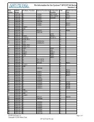
<strong>Pin</strong> Name<strong>Pin</strong> Type (1st, 2nd, &3rd Function)<strong>Pin</strong> DescriptionSupply and Reference <strong>Pin</strong>s<strong>Pin</strong> Information for the Cyclone EP1C6 DeviceVersion 1.5VCCIO[1..4]PowerThese are I/O supply voltage pins for banks 1 through 4. Each bank can support a different voltagelevel. VCCIO supplies power to the output buffers for all I/O standards. VCCIO also supplies power tothe input buffers used for the LVTTL, LVCMOS, 1.5-V, 1.8-V, 2.5-V, and 3.3-V PCI I/O standards.VCCINTPowerThese are internal logic array voltage supply pins. VCCINT also supplies power to the input buffersused for the LVDS, SSTL2, and SSTL3 I/O standards.GND Ground Device ground pins. All GND pins should be connected to the board GND plane.VREF[0..2]B[1..4]I/O, InputInput reference voltage for banks 1-4. If a bank uses a voltage-referenced I/O standard, then these pinsare used as the voltage-reference pins for the bank. If voltage reference I/O standards are not used inthe bank, the VREF pins are available as user I/O pins.VCCA_PLL[1..2] Power Analog power for PLLs[1..2]. The designer must connect this pin to 1.5 V, even if the PLL is not used.GNDA_PLL[1..2] Ground Analog ground for PLLs[1..2]. The designer can connect this pin to the GND plane on the board.GNDG_PLL[1..2] Ground Guard ring ground for PLLs[1..2]. The designer can connect this pin to the GND plane on the board.NC No Connect No connect pins should not be connected on the board. They should be left floating.Configuration and JTAG <strong>Pin</strong>sCONF_DONEBidirectional (open-drain) This is a dedicated configuration status pin; it is not available as a user I/O pin.nSTATUSBidirectional (open-drain) This is a dedicated configuration status pin; it is not available as a user I/O pin.nCONFIGInputDedicated configuration control input. A low transition resets the target device; a low-to-high transitionbegins configuration. All I/O pins tri-state when nCONFIG is driven low.In passive serial configuration mode, DCLK is a clock input used to clock configuration data from anexternal source into the Cyclone device. In active serial configuration mode, DCLK is a clock outputInput (PS mode), Output from the Cyclone device (the Cyclone device acts as master in this mode). This is a dedicated pin usedDCLK(AS mode)for configuration.DATA0 Input Dedicated configuration data input pin.nCEnCEOASDOnCSOInputOutputI/O, OutputI/O, OutputActive-low chip enable. Dedicated chip enable input used to detect which device is active in a chain ofdevices. When nCE is low, the device is enabled. When nCE is high, the device is disabled.Output that drives low when device configuration is complete. During multi-device configuration, this pinfeeds a subsequent device’s nCE pin.Active serial data output from the Cyclone device. This output pin is utilized during active serialconfiguration mode. The Cyclone device controls configuration and drives address and controlinformation out on ASDO. In passive serial configuration, this pin is available as a user I/O pin.Chip select output that enables/disables a serial configuration device. This output is utilized duringactive serial configuration mode. The Cyclone device controls configuration and enables the serialconfiguration device by driving nCSO low. In passive serial configuration, this pin is available as a userI/O pin.CRC_ERRORINIT_DONECLKUSRActive high signal that indicates that the error detection circuit has detected errors in the configurationI/O, OutputSRAM bits. This pin is optional and is used when the CRC error detection circuit is enabled.This is a dual-purpose pin and can be used as an I/O pin when not enabled as INIT_DONE. Whenenabled, the pin indicates when the device has entered user mode. This pin can be used as a user I/OI/O, Output (open-drain) pin after configuration.Optional user-supplied clock input. Synchronizes the initialization of one or more devices. This pin canI/O, Inputbe used as a user I/O pin after configuration.DEV_CLRnI/O, InputDual-purpose pin that can override all clears on all device registers. When this pin is driven low, allregisters are cleared; when this pin is driven high, all registers behave as defined in the design.DEV_OEI/O, InputDual-purpose pin that can override all tri-states on the device. When this pin is driven low, all I/O pinsare tri-stated; when this pin is driven high, all I/O pins behave as defined in the design.MSEL[1..0] Input Dedicated mode select control pins that set the configuration mode for the device.TMS Input This is a dedicated JTAG input pin.TDI Input This is a dedicated JTAG input pin.TCK Input This is a dedicated JTAG input pin.TDO Output This is a dedicated JTAG output pin.Clock and PLL <strong>Pin</strong>sCLK0Input, LVDS InputDedicated global clock input. The dual-function of CLK0 is LVDSCLK1p, which is used for differentialinput to PLL1.CLK1Input, LVDS InputDedicated global clock input. The dual-function of CLK1 is LVDSCLK1n, which is used for differentialinput to PLL1.CLK2Input, LVDS InputDedicated global clock input. The dual-function of CLK2 is LVDSCLK2p, which is used for differentialinput to PLL2.CLK3Input, LVDS InputDedicated global clock input. The dual-function of CLK3 is LVDSCLK2n, which is used for differentialinput to PLL2.DPCLK[7..0]I/ODual-purpose clock pins that can connect to the global clock network. These pins can be used for highfan-out control signals, such as clocks, clears, IRDY, TRDY, or DQS signals. These pins are alsoavailable as user I/O pins.PLL1_OUTpI/O, OutputExternal clock output from PLL 1. This pin can be used with differential or single ended I/O standards. Ifclock output from PLL1 is not used, this pin is available as a user I/O pin.PLL1_OUTnI/O, OutputNegative terminal for external clock output from PLL1. If the clock output is single ended, this pin isavailable as a user I/O pin.PT-EP1C6-1.5Copyright © 2006 <strong>Altera</strong> Corp.<strong>Pin</strong> DefinitionsPage 10 of 13