Simulation, Design and Hardware Implementation of a Low Cost ...
Simulation, Design and Hardware Implementation of a Low Cost ...
Simulation, Design and Hardware Implementation of a Low Cost ...

Create successful ePaper yourself
Turn your PDF publications into a flip-book with our unique Google optimized e-Paper software.
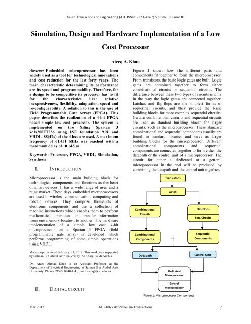
Asian Transactions on Engineering (ATE ISSN: 2221-4267) Volume 02 Issue 01<strong>Simulation</strong>, <strong>Design</strong> <strong>and</strong> <strong>Hardware</strong> <strong>Implementation</strong> <strong>of</strong> a <strong>Low</strong><strong>Cost</strong> ProcessorAteeq A. KhanAbstract -Embedded microprocessor has beenwidely used as a tool for technological innovations<strong>and</strong> cost reduction for the last forty years. Themain characteristic determining its performanceare its speed <strong>and</strong> programmability. Therefore, fora design to be competitive its processor has to fitfor the characteristics like: relativeinexpensiveness, flexibility, adaptation, speed <strong>and</strong>re-configurability. A solution to this is the use <strong>of</strong>Field Programmable Gate Arrays (FPGA). Thispaper describes the realization <strong>of</strong> a 4-bit FPGAbased simple low cost processor. The system isimplemented on the Xilinx Spartan 3xc3s200FT256 using ISE foundation 9.2i <strong>and</strong>VHDL. 88(4%) <strong>of</strong> the slices are used. A maximumfrequency <strong>of</strong> 61.451 MHz was reached with amaximum delay <strong>of</strong> 10.145 ns.Keywords: Processor, FPGA, VHDL, <strong>Simulation</strong>,SynthesisI. INTRODUCTIONFigure 1 shows how the different parts <strong>and</strong>components fit together to form the microprocessor.From transistors, the basic logic gates are built. Logicgates are combined together to form eithercombinational circuits or sequential circuits. Thedifference between these two types <strong>of</strong> circuits is onlyin the way the logic gates are connected together.Latches <strong>and</strong> flip-flops are the simplest forms <strong>of</strong>sequential circuits, <strong>and</strong> they provide the basicbuilding blocks for more complex sequential circuits.Certain combinational circuits <strong>and</strong> sequential circuitsare used as st<strong>and</strong>ard building blocks for largercircuits, such as the microprocessor. These st<strong>and</strong>ardcombinational <strong>and</strong> sequential components usually arefound in st<strong>and</strong>ard libraries <strong>and</strong> serve as largerbuilding blocks for the microprocessor. Differentcombinational components <strong>and</strong> sequentialcomponents are connected together to form either thedatapath or the control unit <strong>of</strong> a microprocessor. Thecircuit for either a dedicated or a generalmicroprocessor in the end will be produced bycombining the datapath <strong>and</strong> the control unit together.Microprocessor is the main building block fortechnological components <strong>and</strong> functions as the heart<strong>of</strong> smart devices. It has a wide range <strong>of</strong> uses <strong>and</strong> ahuge market. These days embedded microprocessorsare used in wireless communication, computing <strong>and</strong>robotic devices. They comprise thous<strong>and</strong>s <strong>of</strong>electronic components <strong>and</strong> use a collection <strong>of</strong>machine instructions which enables them to performmathematical operations <strong>and</strong> transfer informationfrom one memory location to another. The hardwareimplementation <strong>of</strong> a simple low cost 4-bitmicroprocessor on a Spartan 3 FPGA (fieldprogrammable gate array) is developed whichperforms programming <strong>of</strong> some simple operationsusing VHDL.CombinationalCircuitsCombinationalComponentsTransistorsGatesFlip-FlopsSeq. CircuitsSequentialComponentsManuscript received February 11, 2012. This work was supportedby Salman Bin Abdul Aziz University, Al Kharj, Saudi Arabia.DatapathControl UnitDr. Ateeq Ahmad Khan is an Assistant Pr<strong>of</strong>essor at theDepartment <strong>of</strong> Electrical Engineering at Salman Bin Abdul AzizUniversity. Phone-+966508840934 , Email ateeq@ksu.edu.saDedicatedMicroprocessorII.DIGITAL CIRCUITGeneralMicroprocessorFigure 1: Microprocessor ComponentsroMar 2012 ATE-10227012©Asian-Transactions 7
Asian Transactions on Engineering (ATE ISSN: 2221-4267) Volume 02 Issue 01III.MICROPROCESSOR DESIGNThis microprocessor performs the followinginstructionsGeneralformaLDA< taddr>ADDSUBJZJCANDObjectInstruction codeOperation Comment8 A loadAccumulatorAAr>B -MCDECMA 0If Z=1 thenPCIf C=1 thenPCMdirectAddAccumulatordirectSubAccumulatordirectJump onZero flag setJump onCarry flagsetlogic ANDAccumulatordirectComplementOperationINCA 2 IncrementAccumulatorDCRA 4 -1DecrementAccumulatorHLT 6 Halt Halt CPUA=AccumulatorM= Memoryaddr= AddressZ=Zero FlagC= Carry FlagTable 1: Instruction SetPC= Program CounterThe details about the design <strong>and</strong> actual architecture<strong>of</strong> the control unit, what operation code (opcode) isassigned to each <strong>of</strong> the instructions <strong>and</strong> how manybits are to be encoded in an instruction <strong>and</strong> what arethe control words used in micro program are given incontrol unit <strong>of</strong> microprocessor.III.(i)MEMORYAt first the memory was created as R<strong>and</strong>omAccesses Memory (RAM) with 16 words <strong>of</strong> 4-bits, inorder to support the store <strong>and</strong> load instructions, butsince our design has no actual inputs the memory wasturned into a Read Only Memory (ROM) with samesize so we can store our program that we want themicroprocessor to execute. As a result the storeoperation was canceled <strong>and</strong> subsequently theconnection between the accumulator <strong>and</strong> the memorywas eliminated.III.(ii) CONTROL UNIT DESIGNThe purpose <strong>of</strong> the control unit is to initiate aseries <strong>of</strong> sequential steps <strong>of</strong> micro-operations. Duringany given time, certain operations are to be initiatedwhile all others remain idle. Thus, the controlvariables at any given time can be represented by astring <strong>of</strong> l’s <strong>and</strong> 0's called a control word. As such,control words can be programmed to initiate thevarious components in the system in an organizedmanner. A control unit whose control variables arestored in a memory is called a micro program controlunit. Each control word <strong>of</strong> memory is called amicroinstruction, <strong>and</strong> a sequence <strong>of</strong> microinstructionsis called a micro program since alteration <strong>of</strong> themicro program is seldom needed, the control memorycan be a ROM. The use <strong>of</strong> a micro program involvesplacing all control variables in words <strong>of</strong> the ROM foruse by the control unit through successive readoperations. The content <strong>of</strong> the word in the ROM at agiven address determines the micro operations for thesystem. Figure 2 illustrates the general configuration<strong>of</strong> the micro program control unit. The controlmemory is assumed to be a ROM, within which allcontrol information is permanently stored. Thecontrol memory address register specifies the controlword read from control memory. It must be realizedthat a ROM operates as a combinational circuit, withthe address value as the input <strong>and</strong> the correspondingword as the output. The content <strong>of</strong> the specified wordremains on the output wires as long as the addressvalue remains in die address register, no read signalis needed as in a r<strong>and</strong>om-access memory. The wordout <strong>of</strong> the ROM should be transferred to a bufferregister if the address register changes while theROM word is still in use. If the change in address<strong>and</strong> ROM word can occur simultaneously, no bufferregister is needed.Mar 2012 ATE-10227012©Asian-Transactions 8
Asian Transactions on Engineering (ATE ISSN: 2221-4267) Volume 02 Issue 01The word read from control memory represents amicroinstruction. The microinstruction specifies oneor more micro operations for the components <strong>of</strong> thesystem. Once these operations are executed, thecontrol unit must determine the next address. Thelocation <strong>of</strong> the next microinstruction may be the nextone in sequence, or it may be located somewhere elsein the control memory. For this reason, or it isnecessary to use some bits <strong>of</strong> the microinstruction tocontrol the generation <strong>of</strong> the address for the nextmicroinstruction. The next address may also be afunction <strong>of</strong> external input conditions. While themicro operations are being executed, the next addressis computed in the next-address generator circuit <strong>and</strong>then transferred (with the next clock pulse) into thecontrol address register to read the nextmicroinstruction.III.(iii) CONTROL MEMORYControl memory is a ROM with 6-bitaddress given as 64 words, but actually only the first48 are used. Each word is 23-bit long <strong>of</strong> which themost significant 13-bit are sent to the datapath ascontrolling signals determining how each componentin the datapath behaves subject to what kind <strong>of</strong>operation is being preformed. The 6-bits after thecontrol bits in the control word are the brunch bitswhich make the ROM jump from one word toanother if needed depending on the status conditionscoming from the datapath particularly the zero <strong>and</strong>carry flags as well as the signals from the IR . The 4least significant bits in the control word are thecondition selectors which select one <strong>of</strong> the statusconditions to be checked if needed <strong>and</strong> do so byserving as the selecting signals for a 16X1multiplexer where the output <strong>of</strong> the multiplexer is thecontrol signal for the MPC. Based on this way <strong>of</strong>operating, the controlling words were created. Afterthat the VHDL code was written for it <strong>and</strong> simulated.A simple behavioral model was used for creating theROM. Since it is a read-only memory, no clocksignal or write-enable pin is necessary. The circuitcontains a pile <strong>of</strong> pre-stored words, being the oneselected by the address input (addr) presented at theoutput (data).III.(iv)MICROPROCESSOR CONNECTIONSFigure 2: Control Unit ArchitectureThe microprocessor is built by connectingthe datapath with the control unit. This is done byusing the same method in creating the datapath <strong>and</strong>control unit which is port mapping <strong>of</strong> the structuralmodel, with the inputs being a clock signal to helpregulate the transfer <strong>of</strong> data inside themicroprocessor, <strong>and</strong> a reset signal to make themicroprocessor go to the start <strong>of</strong> the control wordsstored in the ROM by resetting the MPC which holdsthe address <strong>of</strong> the ROM. The microprocessor has a 4-bit output which is the result <strong>of</strong> the instructionsexecuted by it.The program stored in the memory <strong>of</strong> the datapathwhich defines the instructions that will be executed<strong>and</strong> the order they are executed in, can be written inany manner seen appropriate for a specificfunction(s) that the microprocessor is intended toperform. The only limitation is that the space inwhich the instructions can be stored is limited to 16word, bearing in mind that some instructions needtwo words while other need only one word <strong>of</strong> space.The program written is designed to test all <strong>of</strong> theMar 2012 ATE-10227012©Asian-Transactions 9
Asian Transactions on Engineering (ATE ISSN: 2221-4267) Volume 02 Issue 01Figure 3: The Microprocessor Behavioral <strong>Simulation</strong>Figure 4: The Microprocessor Timing <strong>Simulation</strong>instructions the microprocessor can perform in orderto determine the success <strong>of</strong> this paper.The behavioral simulation has been done to ensurethat the microprocessor performs the program storedin its memory, after that the place <strong>and</strong> routesimulation (timing simulation) is done to find out theMar 2012 ATE-10227012©Asian-Transactions 10
Asian Transactions on Engineering (ATE ISSN: 2221-4267) Volume 02 Issue 01delay <strong>and</strong> if it is too much that it could hinder theperformance <strong>of</strong> the microprocessor. Both simulationsare shown in figure 3 <strong>and</strong> figure 4.IV. CONCLUSIONA large number <strong>of</strong> low cost prototype boardsavailable for various FPGAs. This is certainly nottrue for ASICs as the tool cost alone can beprohibitive in many cases. The other reason for thelow setup cost is that the use <strong>of</strong> an FPGA means thatthe mask costs associated with an ASIC are avoidedwhich can be a significant saving for a moderntechnology.The design <strong>of</strong> the microprocessor isanalyzed carefully to ensure that any failure would becorrected, this is done at each step making sure thatevery component is functioning accurately on its own<strong>and</strong> also when it is connected to other parts. Themeasure <strong>of</strong> accuracy is the simulation which couldgive a clear picture on how the component performsas well as helping in finding what causes failureswhen they occur.FPGA-based 4-bit microprocessor on XilinxSpartan 3 board is successfully implemented usingVHDL language. The microprocessor is made <strong>of</strong> thecontrol unit, an arithmetic logic unit (ALU), amemory unit <strong>and</strong> registers. The processor has amaximum frequency <strong>of</strong> 61.451 MHz <strong>and</strong> 88 slices areutilized. It can perform ten different instructions asdescribed in the specifications <strong>of</strong> the microprocessor.<strong>Simulation</strong>s are done to ensure its functionality.The microprocessor can be upgraded by adding thestore instruction to it by changing the datapathmemory into a RAM, also by increasing the number<strong>of</strong> bits the microprocessor can process; it could beused in many applications.As far as the future work is concerned, latestXilinx with new family <strong>of</strong> FPGA can be used to forspeed improvement <strong>and</strong> area reduction. Altera can betried for comparison <strong>of</strong> two technologies.REFERENCES[1] Enoch O. Hwang, “Digital Logic <strong>and</strong>Microprocessor <strong>Design</strong> with VHDL”, Brooks Cole,2005.[2] Volnei. A. Pedroni, “Circuit <strong>Design</strong> with VHDL”,Massachusetts, MIT Press, 2004.[3] Pierre-Emanuel Gaillardon, M.Haykel Ben Jamma,Giovanni Betti Benevetti, Fabien Clermidy, LucaPerniola, “Emerging Memory Technologies forReconfigurable Routing in FPGA architecture”;IEEE International Conference on Electronics,Circuits <strong>and</strong> Systems (ICECS)-invited paper,December 2010.[4] J.Rose <strong>and</strong> D.Hill, “ Architectural <strong>and</strong> Physical <strong>Design</strong>Challenges for One-Million Gate FPGAs <strong>and</strong>Beyond”, Proceedings <strong>of</strong> the ACM FifthInternational Symposium on Field-ProgrammableGate arrays, pp.129-132, Feb.1997.[5] Singh, et.al. “A Novel High ThroughputReconfigurable FPGA Architecture”, Proceedings <strong>of</strong>the ACM/SIGDA Symposium on Field-Programmable Gate arrays, pp. 22-29, Feb.2000.[6] M. Abd-El-Barr <strong>and</strong> H. El-Rewini, “Fundamentals<strong>of</strong> Computer Organization <strong>and</strong> Architecture”, NewJersey, John Wiley & Sons. Inc, 2005.[7] E. Ayeh, K. Agbedanu, Y. Morita, O. Adamo, <strong>and</strong> P.Guturu, “FPGA <strong>Implementation</strong> <strong>of</strong> an 8-bit SimpleProcessor”, in the proceedings <strong>of</strong> Region 5Conference, 2008 IEEE held in Kansas City, MO,April 2008.[8] Baker, R. Jacob (2010). “CMOS: Circuit <strong>Design</strong>,Layout, <strong>and</strong> <strong>Simulation</strong>”, Third Edition. Wiley-IEEE.pp. 1174. ISBN 978-0-470-88132-3. http://CMOSedu.com/[9] Wiśniewski,Remigiusz . “Synthesis <strong>of</strong> compositionalmicroprogram control units for programmabledevices”. Zielona Góra: University <strong>of</strong> Zielona Góra.pp. 153. ISBN 978-83-7481-293-1.2009.[10] Ralph D. Wittig <strong>and</strong> Paul Chow. “OneChip: AnFPGA Processor with Reconfigurable Logic”. In TheFourth Annual IEEE Symposium on FPGAs forCustom Computing Machines FCCM'96, pages 126-135. IEEE, March 1996[11] P. A. Wilsey T. J. McBrayer, <strong>and</strong> D. Sims, "TowardsA Formal Model <strong>of</strong> VLSI Systems Compatible withVHDL," VLSI '91, A. Halaas <strong>and</strong> P. B. Denyer(eds), Elsevier Science Publishers B.V. (North-Holl<strong>and</strong>), 225-236, 1991.[12] M. Kauppi <strong>and</strong> J-P. Soininen, "FunctionalSpecification <strong>and</strong> Verification <strong>of</strong> Digital Systemsusing VHDL Combined with Graphical StructuredAnalysis," EuroVHDL, 1991[13] D. Borrione <strong>and</strong> J. L. Paillet, "An approach to theformal verification <strong>of</strong> VHDL descriptions,"IMAG/Artemis, Grenoble, November 1987.[14] S. Hadjis, A. Canis, J.H. Anderson, J. Choi, K. Nam,S. Brown. T. Czajkowski, "Impact <strong>of</strong> FPGAarchitecture on resource sharing in high-levelsynthesis," to appear in the ACM/SIGDAInternational Symposium on Field ProgrammableGate Arrays, to be held at Monterey, CA, February2012.[15] M. H. Ben Jamaa, D. Atienza, Y. Leblebici, <strong>and</strong> G.De Micheli. “Programmable Logic Circuits Basedon Ambipolar CNFET”. <strong>Design</strong> AutomationConference (DAC), Anaheim, California, USA,2008.[16] Krishna Kant “Microprocessors <strong>and</strong>Microcontrollers: Architecture Programming AndSystem Desig n”. PHI Learning Pvt. Ltd.,2007 ISBN 8120331915 page 61, describing theiAPX 432[17] Gerry Kane, Adam Osborne “16 Bit MicroprocessorH<strong>and</strong>book”. ISBN 0079310435 (0-07-931043-5)Mar 2012 ATE-10227012©Asian-Transactions 11
Asian Transactions on Engineering (ATE ISSN: 2221-4267) Volume 02 Issue 01[18] L.Sterpone, M. Violante. “Hardening FPGA-basedsystems against SEUs: A new design methodology”.Academy Publisher Journal <strong>of</strong> Computers, Vol.1,No.1, April 2006, pp.22-30.[19] JD Plummer, M.D. Deal, P.B. Griffin, “Silicon VLSITechnology”, Prentice Hall Inc., USA, 2000[20] A.Singh, et al. “ A Novel High ThroughputReconfigurable FPGA Architecture”, Proceedings <strong>of</strong>the ACM/SIGDA International Symposium on FieldProgrammable Gate Arrays, pp. 22-29. Feb 2000.Ateeq Ahmad Khan was born in India in 1955. Heobtained his PhD in Electronics Engineering fromAligarh Muslim University in 1999.He joined as Assistant Pr<strong>of</strong>essor in AMU in 1981 <strong>and</strong>was promoted as Associate Pr<strong>of</strong>essor in 1987. Later,he joined Electrical Engineering Department, College<strong>of</strong> Engineering, King Saud University, Riyadh in 2003<strong>and</strong> then joined Salman Bin Abdul Aziz University atAl Kharj <strong>and</strong> is presently continuing there. Dr. Khan isa fellow <strong>of</strong> Institute <strong>of</strong> Electronic <strong>and</strong>Telecommunication Engineering IETE <strong>and</strong> seniormember <strong>of</strong> Institution <strong>of</strong> Engineers, India.Mar 2012 ATE-10227012©Asian-Transactions 12