file no service manual led tv - Panasonic
file no service manual led tv - Panasonic
file no service manual led tv - Panasonic

Create successful ePaper yourself
Turn your PDF publications into a flip-book with our unique Google optimized e-Paper software.
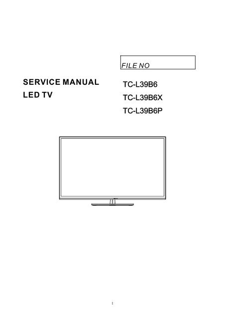
FILE NOSERVICE MANUALLED TVTC-L39B6TC-L39B6XTC-L39B6P1
CONTENTS1. Safety precautions .................................................................................................32. Alignment instructions and method of software upgrading.....................................53. Working principle analysis of the unit ................................................................... 124. Specifications.......................................................................................................135. Block diagram ......................................................................................................146. IC block diagram..................................................................................................177. Wiring diagram ...................................................................................................248. Troubleshooting guide..........................................................................................299. Schematic diagram ..............................................................................................3310. APPENDIX-A: Assembly listAPPENDIX-B: Exploded View11. Disassembly and Assembly Instructions2
Attention: This <strong>service</strong> <strong>manual</strong> is only for <strong>service</strong> personnel to take reference with. Before servicingplease read the following points carefully.Safety precautions1. InstructionsBe sure to switch off the power supply before replacing or welding any components orinserting/plugging in connection wire Anti static measures to be taken (throughout the entire productionprocess!):a) Do <strong>no</strong>t touch here and there by hand at will;b) Be sure to use anti static electric iron;c) It’s a must for the welder to wear anti static gloves.Please refer to the detai<strong>led</strong> list before replacing components that have special safety requirements.Do <strong>no</strong>t change the specs and type at will.2. Points for attention in servicing of LED2.1 Screens are different from one model to a<strong>no</strong>ther and therefore <strong>no</strong>t interchangeable. Be sure toUse the screen of the original model for replacement.2.2 The operation voltage of LED screen is high voltage. Be sure to take proper measures inprotecting yourself and the machine when testing the system in the course of <strong>no</strong>rmal operation orright after the power is switched off. Please do <strong>no</strong>t touch the circuit or the metal part of the moduleThat is in operation mode. Relevant operation is possible only one minute after the power is switchedoff.2.3 Do <strong>no</strong>t use any adapter that is <strong>no</strong>t identical with the TV set. Otherwise it will cause fire or damageto the set.2.4 Never operate the set or do any installation work in bad environment such as wet bathroom,laundry, kitchen, or nearby fire source, heating equipment and devices or exposure to sunlight etc.Otherwise bad effect will result.2.5 If any foreign substance such as water, liquid, metal slices or other matters happens to fall into themodule, be sure to cut the power off immediately and do <strong>no</strong>t move anything on the module lest it shouldcause fire or electric shock due to contact with the high voltage or short circuit.2.6 Should there be smoke, ab<strong>no</strong>rmal smell or sound from the module, please shut the power off atonce. Likewise, if the screen is <strong>no</strong>t working after the power is on or in the course of operation, thepower must be cut off immediately and <strong>no</strong> more operation is allowed under the same condition.2.7 Do <strong>no</strong>t pull out or plug in the connection wire when the module is in operation or just after thepower is off because in this case relatively high voltage still remains in the capacitor of the drivingcircuit. Please wait at least one minute before the pulling out or plugging in the connection wire.2.8 When operating or installing LED please don’t subject the LED components to bending, twisting orextrusion, collision lest mishap should result.2.9 As most of the circuitry in LED TV set is composed of CMOS integrated circuits, it’s necessary topay attention to anti statics. Before servicing LED TV make sure to take anti static measure andensure full grounding for all the parts that have to be grounded.2.10 There are lots of connection wires between parts behind the LED screen. When servicing ormoving the set please take care <strong>no</strong>t to touch or scratch them. Once they are damaged the screenwould be unable to work and <strong>no</strong> way to get it repaired.If the connection wires, connections or components fixed by the thermo tropic glue need to disengagewhen <strong>service</strong>, please soak the thermo tropic glue into the alcohol and then pull them out in case ofdamage.3
2.11 Special care must be taken in transporting or handling it. Exquisite shock vibration may lead tobreakage of screen glass or damage to driving circuit. Therefore it must be packed in a strong casebefore the transportation or handling.2.12 For the storage make sure to put it in a place where the environment can be control<strong>led</strong> so as toprevent the temperature and humidity from exceeding the limits as specified in the <strong>manual</strong>. Forprolonged storage, it is necessary to house it in an anti-moisture bag and put them altogether in oneplace. The ambient conditions are tabulated as follows:Temperature Scope for operation 0 ~ + 35 o CScope for storage-20 ~ + 60 o CHumidity Scope for operation 20% ~ 80 %Scope for storage 10% ~ 90%2.13 Display of a fixed picture for a long time may result in appearance of picture residue on thescreen, as commonly cal<strong>led</strong> “ghost shadow”. The extent of the residual picture varies with the makerof LED screen. This phe<strong>no</strong>me<strong>no</strong>n doesn’t represent failure. This “ghost shadow” may remainin the picture for a period of time (several minutes). But when operating it please avoid displaying stillpicture in high brightness for a long time.3. Points for attention during installation3.1 The front panel of LED screen is of glass. When installing it please make sure to put it in place.3.2 For <strong>service</strong> or installation it’s necessary to use specified screw lest it should damage the screen.3.3 Be sure to take anti dust measures. Any foreign substance that happens to fall down between thescreen and the glass will affect the receiving and viewing effect3.4 When dismantling or mounting the protective partition plate that is used for anti vibration andinsulation please take care to keep it in intactness so as to avoid hidden trouble.3.5 Be sure to protect the cabinet from damage or scratch during <strong>service</strong>, dismantling or mounting.4
2. Alignment instructions(1) Test equipmentVG-859 (YPbPr, VGA, HDMI signal generator)FLUKE 54200(TV signal generator)CA310 (white balancer)(2) Power testConnect main board, power board and IR board according the wiring diagram, connectthe power and press power key (Remote controller or Keypad) button to turn on the TV.a) Test the pin voltage of P802/power board , the data is shown in table1:Table1 voltage data of P802For 39”P802 Pin1,2 Pin3,4 Pin5,6,7 Pin8,9 Pin10,11Voltage GND 11.4V~12.6V GND 11.4V~12.6V 4.75V~5.25VFor 39”Pin12 Pin13 Pin 14 Pin15 Pin16On:2.5V~5.25VOff: 0~0.5VNormal: 2.0~5VAb<strong>no</strong>rmal :0~0.5VOn:2.5V~5.25VOff: 0~0.5VDuty 5%~100%NC5
(3) Alignment flow-chartThe alignment flow-chart is shown as fig-1Check if EDID, HDCP KEY, FLASH are writtenCombined test for general assemblyAuto Gamma adjustmentConnect to the center signal source and check eachFunction of TV (station leaking, analog control, etc.)Check the output of speaker.Input AV signal and check the functionInput HD signal and check the function of YPbPrInput USB signal and check if the display is <strong>no</strong>rmal, checkthe function (analog control), horizontal/vertical center, etc.Input HDMI signal and check if the display is <strong>no</strong>rmal, checkthe function (analog control), horizontal/vertical center, etc.Checking SPDIF will output the signal on Amplifier.Preset ex-factoryCheck the accessories and packingFig-1 adjustment flow-chart6
(4) Adjustment instructionAt any input source then press the “←”, “EXIT” and “OK” (using RC within 1 sec) to enter factory modeDuring Factory menu, if “EXIT” key is pushed, system will exit factory mode.4-1. Auto Gamma Adjustment & Check4-2.1. Set into factory mode then choose Auto Gamma Adjust,4-2.2. Press "2" "3" "2" "4" in turn within 1sec to enter the item, and push Init will self-generate gray patternfor adjusting.4-2.3. Following the Cool spec as bellow.ColorxyAdjustToleranceCool100IRE 0.266250IRE 0.2658100IRE 0.266750IRE 0.2654±0.005(1) Adjust 100IREFirst, Decrease G to meet y spec(0.2667).Second, Decrease R to meet x spec(0.2662).(2) Adjust 50IREFirst, Decrease G to meet y spec(0.2654).Second, Decrease R to meet x spec(0.2658).Note: Do <strong>no</strong>t adjust the B GAIN on both 100IRE and 50IRE.When match the spec, pressing “Save” then exit the adjustment page.(3) When match the spec, pressing right key in "Save" position then exit the adjustment page.4-2.4. Exit Factory Mode:After finish Gamma adjust press [EXIT] to exit factory mode.7
(5) Items of Factory menuWhen in any source, press the “Left -> Exit -> OK” key of remote control can enter into factory mode.During Factory menu, only “EXIT” key is pushed, system will exit factory mode.Press up and down key can move high light item from Model Change -> Color Temp. Adjust -> Auto GammaAdjust -> Timer Clear -> Preset Channel -> Full Power -> ADC Calibration -> Shipping reset -> Bypass Gamma ->UART Enable -> I2C -> Boot Loader Upgrade -> V-Com Adjust -> SG Pattern.Push “Enter” key can enter high light item function. (Press left and right can adjust value)Display Model version, Release Date, firmware version and released date on the bottom.1)Model IDPress up or down key can select high light item functionPress enter or right key to enter the item.It's only used for FW engineer.2)Color Temp. AdjustPress up or down key can select high light item functionPress enter or right key to enter the item.It's only used for PQ engineer.3)Auto Gamma AdjustPress up or down key can select high light item functionPress enter or right key to enter the item.It's only used for PQ engineer.4)Timer ClearReset the timer which records hours of LED panel burn inThis item will have a check dialog “yes or <strong>no</strong>” to do or <strong>no</strong>t.- Time in factory mode: Time function shall be displayed automatically. Saving the total time of systempower on (LED turn on), and count the time automatically. The timer is continuous and saved (per 10minutes) forever, unless it will be reset by doing “Timer Clear”.5)Preset channelLoad preset channel for production line.6)Full PowerThis is for power consumption testing.To measure the maximum power consumption of TV set, we adjust the value of following items tomaximum.- Video: Contrast maximum value, Brightness maximum value, Backlight maximum value.- Audio: Volume maximum value, Bass default value, Treble default value.Press enter key to turn on Full Power and OSD stay display until press enter key to recover from FullPower.8
7)ADC CalibrationADC Calibration function is reserved for calibration by hand (PQ engineer only).8)Shipping resetReset all settings of OSD menu to default value.Reset settings: Channel table, Model table (H/V Position, Clock, Phase), Source dependent setting(Contrast, Brightness etc.), Common setting (Volume, Language etc.), Parental Control (Rating,Password etc), Closed Caption.9)Bypass GammaFor factory test value of gamma.10)UART EnableEnable to communicate with Auto-Alignment system.11)I2CEnable to communicate with Eeprom burn-in tool.12)Boot Loader UpgradeFor firmware downgrade used.13)V-Com AdjustIt's reserved for BMS function.14)SG PatternAging is for factory burn in and PTN ID provides each pattern for tester using.(6) Performance check6-1 TV functionConnect RF to the center signal source, enter Channel menu → auto tuning, check if there are channels beskipped, check if the picture and speaker are <strong>no</strong>rmal.6-2 AV terminalsInput Video signal, check if the picture and sound are <strong>no</strong>rmal.6-3 YPbPr terminalInput YUV signal (VG859 signal generator), separately input the YUV signals listed in table4 and check if thedisplay and sound are <strong>no</strong>rmal at any situation (power on, channel switch and format convert, etc.)Table4 YUV signal formatFREQPERIODSYNCPOLARITYPIXELCLOCKDisplaySYNCWIDTHBACKPORCHMODELINE(kHz)FRAME(Hz)LINE (pixel)FIELD(lines)LINEFIELD(MHz)LINE (pixel)FRAME(lines)LINE (pixel)FRAME(lines)LINE (pixel)FRAME(lines)15.734 1716 Negitive 27 1440 124 11459.94Hz 720x480i 59.94 525 Negitive 480 3 1531,469 858 Negitive 27 720 62 6059.94Hz 720x480P 59.94 525 Negitive 480 6 3045 1650 Positive 74.25 1280 40 22060Hz 1280x720P 60 750 Positive 720 5 2033.75 2200 Positive 74.25 1920 44 14860Hz 1920X1080i 60 1125 Positive 1080 5 1567.5 2200 Positive 148.5 1920 44 14860Hz 1920X1080P 60 1125 Positive 1080 5 369
6-4 HDMI terminalInput HDMI signal (VG859 signal generator), separately input the signals listed in table6 and check the display andsound (32 KHz, 44.1 KHz, 48 KHz) at any situation (power on, channel switch and format convert, etc.)Table6 HDMI signal formatHDMI1/2/DVITimingTableFREQ FREQ PERIODSYNCPOLARITYPIXELCLOCKDisplaySYNCWIDTHBACKPORCHMODELINE(kHz)FRAME(Hz)LINE (pixel)FIELD(lines)LINEFIELD(MHz)LINE (pixel)FRAME(lines)LINE (pixel)FRAME(lines)LINE (pixel)FRAME(lines)31.47 800 Negitive 25.175 640 96 48640x480 59.94 525 Negitive 480 2 3337.88 1056 Positive 40 800 128 88800x600 60.32 628 Positive 600 4 2348.36 1344 Negitive 65 1024 136 1601024x768 60 806 Negitive 768 6 2947.4 1440 Positive 68.25 1280 32 801280x768 (1280cvt) 59.99 790 Negitive 768 7 1247.78 1664 Negitive 79.5 1280 128 1921280x768 59.87 798 Positive 768 7 2063.98 1688 Positive 108 1280 112 2481280x1024 60.02 1066 Positive 1024 3 3847.71 1792 Positive 85.5 1360 112 2561360x768 60.02 795 Positive 768 6 1847.71 1792 Positive 85.5 1366 112 2561366x768 59.79 795 Positive 768 6 1867.5 2200 Positive 148.5 1920 44 1481920x1080 60 1125 Positive 1080 5 3615.73 1716 Negitive 27 1440 124 11459.94Hz 1440x480i 59.94 262.5 Negitive 480 3 1531.47 858 Negitive 27 720 62 6059.94Hz 720x480P 59.94 525 Negitive 480 6 3045 1650 Positive 74.25 1280 40 22060Hz 1280x720P 60 750 Positive 720 5 2033.75 2200 Positive 74.25 1920 44 14860Hz 1920X1080i 60 562.5 Positive 1080 5 1527 2750 Positive 74.25 1920 44 14824Hz 1920x1080P 24 1125 Positive 1080 5 3633.75 2200 Positive 74.25 1920 44 14830Hz 1920x1080P 30 1125 Positive 1080 5 3667.5 2200 Positive 148.5 1920 44 14860Hz 1920X1080P 60 1125 Positive 1080 5 3610
6-5 other functions checka) Check the sleep timer, picture/sound mode, OSD, stereo and analog TV Teletext, etc.(7) Firmware update process(1) Plug the USB with the firmware <strong>file</strong> named upgrade_2013_NA_60.pkg(2) If system detect upgrade_2013_NA_60.pkg, USB upgrade message would appear automatically.(3) Press Up key to select Yes, and then press OK key to start the upgrading.(4) Upgrading is starting, please wait for the progress finish.(5) When the progress completed, please follow the instruction to remove USB and restart Power offthen on.11
3. Working principle analysis of the unit1. NTSC signals flow:Antenna signal will be send to tuner TDST-H021F, then Tuner will be demodulating andoutput standard video signal TV-CVBS, and sound SIF signal.TV-CVBS will send to the master control IC MT5385 to video decode, de-interlace and scaler, the<strong>no</strong>utput LVDS level drive for panel display.The sound IF (SIF) will be fed into MT5385, after demodulating, pre-amplifying, bass adjusting andvolume control, the sound signal will be transform into digital I2S signal and sent todigital amplifier TAS5707.2. Composite/Component signal flowComposite signal and Component signal will be fed to MT5385 to perform video decode, deinterlaceand scaler, then output LVDS drive level for panel display.Audio signal from Composite/Component terminal via matched resistance is fed to MT5385 to bassadjust and volume control, the sound signal will be transform into digital I2S signal and sentto digital amplifier TAS5707.3. HDMI signal flowTwo HDMI video signals are directly fed to the master control IC MT5385 to digital decode, imagescale, then output LVDS drive level for panel display. HDMI audio signal via decoder built-in MT5385 tobass adjust and volume control, the sound signal will be transform into digital I2S signal andsent to digital amplifier TAS5707.4. USB signal flowUSB signal via USB connector sent to MT5385 and its A/D conversion to YPbPr output forMT5385, then output R/G/B of 24 bit to back end module to Video decode, de-interlace andimage scale, then send to LVDS level drive for panel display.Sound signal of USB signal via matched resistance and sent to MT5385 to bass adjust andvolume control, the sound signal will be transform into digital I2S signal and sent to digitalamplifier TAS5707.5. SPDIF signal flowThe master control IC MT5385 will transfer digital sound signal out by format Dobly Digital or PCM.12
4. Specifications13
5-1 Block DiagramEE:SPD39T 39” Block DiagramA70 60Hz Models byMTK MT5835 PlatformWXGA :2x10Full-HD :2x20Panel outR_outAudioAMPTAS5707L_outDDR3 1G-1600H5TQ1G63DFR-PBCFlash 16MBMX25L12845EMI-10GDTV system ICAudio I2S outputMTKIF +/-MT5385EEPROM 64KB24C32KeypadCVBS/Y Pb Pr& Audio R/LCrystal27MHzIREnableYARCBufferIR / LED-RBoardTunerLGTDST-H021F5-1 Block DiagramANT /CABLEPower board:FSPPbPrLRCOLOR STREAM HD& COMPOSITE IN& Audio R/L inS/PDIFSPE39T 39” Block DiagramSPDIFOUTHDMI 114HDMI 2USB
Power Board: FSP15
Power Board: DARFON16
6. IC block diagram1. MT5385GENERAL FEATURE LISTHost CPU ARM11 single core 700MHz Floating Point Unit 16K I-Cache and 16K D-Cache for ARM11 core 128K L2 Cache Boot ROM Boot from serial flash, NAND flash Supports security boot JTAG ICE interface Watch Dog timersGeneral Copy Protection Unit Supports CPPM/CPRM Supports AES with 128/192/256 bit key Supports AACS Supports DES/3DES Supports SHA-1/224/256 Supports MD5 Supports CSS Supports RC4 Random number generatorMPEG1 DecoderMPEG2 Decoder MPEG MP@ML, MP@HL Supports de-blocking filter Full-HD 30P dual decoderMPEG4 Decoder (option) ASP@L5 Full-HD 30P dual decoderH.264 (MPEG4.10 / AVC) HD Decoder (option) MP@L4.0, HP@L4.0, constrained BP@L3 video standard Full-HD 30P dual decoderVC-1 (SMPTE421M) Decoder (option) MP@HL, AP@L3 WMV9 decoder MP@HL Full-HD 30P dual decoderDivX (XviD) Decoder (option)17
DIVX3 / DIVX4 / DIVX5 / DIVX6 / DIVX HD Full-HD 30P dual decoderAVS Decoder (option) Jizhun pro<strong>file</strong> @Level 6.2 (supports 4:2:0 format) Full-HD 30P dual decoderRMVB Decoder (option) RealVideo8/9/10 Full-HD 30P dual decoderVP6 Decoder (option)VP8 Decoder (option) Supports 3D side-by-side Full-HD contents Full-HD 30P dual decoderMVC H.264 stereo high pro<strong>file</strong> Full-HD 60fpsStill Image decoding JPEG decoder (base-line or progressive), hardware accelerator BMP/PNG/JIF decoderDe-mosquito engine For all AV inputs2D Graphics Supports multiple color modes Point, horizontal/vertical line primitive drawings Rectangle fill and gradient fill functions Bitblt with transparent options Alpha blending and optional pre-multiplied alpha composition Bitblt Stretch Bitblt YCbCr to RGB color space conversion Supports index to direct mode bitbltImage Resizer Supports 16bpp/32bpp direct color format Supports 420/422 video format Supports 420/422/444 JPEG format Arbitrary ratio vertical/horizontal scaling of video, from 1/128X to 128X Simple DMA Supports MMU in OSD modeOSD Plane Three linking list OSDs with multiple color mode and all of them haveup-scaler Supports stereo OSD18
Video Plane Supports video freeze and over scan Flesh tone management Gamma correction Color Transient Improvement (CTI) 2D Peaking Saturation/hue adjustment Brightness and contrast adjustment Black and White level extender Adaptive Luma management Automatic detect video, film and mixed-mode source 3:2/2:2 pull down source detection Supports FHD motion-adaptive de-interlace Supports excellent low angle image processing Brilliant boundary shaping for moving object Advanced <strong>no</strong>n-linear pa<strong>no</strong>rama scaling Programmable zoom viewer Progressive scan output Supports alpha blending for OSD on video plane Dithering processing for flat panel display Frame rate conversion Supports FHD panel and VGA dot-to-dot Supports PIP/POP, (dual de-interlace, one HD and one SD)OD (option) Supports 60Hz Full-HD and WXGA panel over driveTCON (option) Flexible timing control with programmable timing Horizontal timing control Vertical timing control Multi-line timing control Multi-frame timing control Supports gate power modulation timing Supports command-based timing Supports POL inversion every 30 seconds Supports 1/2/4/8 frame inversion, 1-line inversion, 2-line inversion, andcould up to 255-line dot inversionLocal Dimming Block division: up to 800 total blocks, up to 100 horizontal blocks Supports 50K ~ 50M SPI clock rateLVDS19
Supports 6/8/10-bit one-link, 6/8/10-bit dual-link LVDS transmitter Built-in spread spectrum for EMI performance Programmable panel timing outputMini-LVDS Dual port 8-bit 6 pairs mini-LVDS outputCVBS In On-chip 54 MHz 10-bit video ADC Supports PAL (B,G,D,H,M,N,I,Nc), NTSC, NTSC-4.43, SECAM NTSC/PAL supports 3D/2D comb filter Built-in motion-adaptive 3D Noise Reduction VBI data slicer for CC/TT decoding Supports 1 S-Video Supports 2 1-channel CVBS Supports SCART connectorVGA In Supports VGA input up to UXGA 162 MHz Supports full VESA standardsComponent Video In Supports 2 component video inputs Supports 480i / 480p / 576i / 576p / 720p / 1080i / 1080pAudio ADC Supports 3 pair L/R inputAudio digital input Supports 1 bit (2 channel) I2S audio inputHDMI Receiver Two channel HDMI1.4a Maximum data rate can be up to 3.3 GHz Audio return channel EIA/CEA-861B CECVideo bypass ATV bypass CVBS Monitor (any AV or S-video input)TV audio demodulator Supports BTSC / EIA-J / A2 / NICAM / PAL FM / SECAM world-wideformats Standard automatic detection20
Stereo demodulation, SAP demodulation Mode selection (Main/SAP/Stereo)Audio DAC Supports 2-pair audio DACsDRAM Controller 16-bit DDR2/DDR3 interface Supports DDR2 1066Mhz, DDR3 1333Mhz Supports 512Mb or 1Gb or 2Gb DDR2 and DDR3 DRAM device Supports DDR2-1066/DDR3-1333/DDR3-1600 deviceAudio DSP Supports AC-3 (Dolby Digital) decoding (ATSC) and E-AC3 (Dolby DigitalPlus) decoding (option) MPEG-1 layer I/II decoding Supports WMA / HE-AAC (option) Support Dolby DDCO, and MS10 (option) Dolby Prologic II (option) Audio output: 5.1ch + 2ch (down mix) + 2ch(bypass) Pink <strong>no</strong>ise and white <strong>no</strong>ise generator Equalizer Bass management 3D surround processing with virtual surround Audio and video lip synchronization Supports bass/treble Automatic volume control Supports 5-bit (10-channel) main audio I2S output interface, each of these channels is up to 24-bit resolutionS/PDIF interface Supports SPDIF in bypass SPDIF outAnalog TV IF Demodulator Supports world-wide analog TV standard Accept direct IF and low IF Full digital AGC control and carrier recovery Embedded SAW filter and IF Amplifier. Cost effective TV front-endstructure and <strong>no</strong> more cost on: External analog SAW filters (Video/Audio) External analog IF demodulator External peripheral circuit on CVBS signal data path External SAW filter and IF VGA on tuner21
Digital TV (ATSC / Open-Cable) Demodulator Compliant with ATSC digital television standard Supports SCTE DVS-031 and ITU J.83 Annex B digital CATV standard Accept direct IF (44 MHz or 43.75 MHz) and low IF (5.38 MHz) NTSC interference rejection capability Meet all ATSC/A74 requirements Excellent adjacent and co-channel rejection capability Dual digital AGC controls for IF and RF, respectively Full-digital frequency offset recovery with wide acquisitionrange 500KHz for ATSC and 250 kHz for CATVreception EIA/CEA-909 antenna interface, both mode A and mode B are supported Embedded SAW filter and IF Amplifier. Cost effective TV front-endstructure and <strong>no</strong> more cost on: External analog IF demodulator External SAW filter and IF VGA on tunerPeripherals Seven basic serial interfaces: one is for the tuner, three are the masters forgeneral purpose and two of them canbe active in standby mode, one is the slave for VGA DDC, theother two extra slave serial interfaces used forHDMI EDID data Five PWMs, two of them can be active in standby mode IR receiver Real-time clock and watchdog controller Built-in 2-link USB2.0/1.1, both of them support external hub with 16endpoints. Built-in uP for standby mode Supports SDIO interface Supports smart card interface Supports two serial flash or one serial and one NAND flash Supports 2-input low-speed ADC Supports boundary scan (JTAG)IC Outline LQFP Package 216 pins with E-pad 3.3V/1.2V and 1.8V for DDR2 or 1.5V for DDR322
2. TI TAS570720-W STEREO DIGITAL AUDIO POWER AMPLIFIER WITH EQ AND DRC23
7-1 BLOCKSPD39T 39-inch Wiring Diagram24
7-2 Wiring ConnectionLG panelMain board to Panel Main board to SpeakerSPD39T SPD39TPanel side LVDS cable Main board CN1 Main board CN4 Color Speaker Right1 NC NC 1 SPK_OUTL+ Red P3 Speaker +2 NC NC 2 SPK_OUTL- Black P2 Speaker -3 NC NC Left4 NC NC 3 SPK_OUTR- Green P5 Speaker -5 NC NC 4 SPK_OUTR+ White P4 Speaker +6 NC NC7 SELLVDS Yellow 28 LVDS_SEL8 NC NC Main board to IR / Key9 NC NC SPD39T10 NC NC IR board CN1 Color Main board CN311 GND NC 1 VCC3V3_STB Red 1 3V3STB12 R1AN White 40 TX_AO0N 2 IRR White 2 IRR13 R1AP Black 39 TX_AO0P 3 GND Black 3 GND14 R1BN White 38 TX_AO1N 4 LED_G Orange 4 LEDG15 R1BP Brown 37 TX_AO1P NC 5 LEDR16 R1CN White 36 TX_AO2N NC 6 Light_S_C17 R1CP Red 35 TX_AO2P NC 7 Light_S_D18 GND Black 15 GND 1 GND Black 8 GND19 R1CLKN White 34 TX_AOCKN 2 Power Red 9 Power Key25
20 R1CLKP Orange 33 TX_AOCKP 3 SAR0 Orange 10 SAR021 GND Black 16 GND 4 SAR1 Yellow 11 SAR122 R1DN White 32 TX_AO3N23 R1DP Yellow 31 TX_AO3P24 NC NC25 NC NC26 NC NC27 NC NC28 R2AN White 12 TX_AE0N29 R2AP Black 11 TX_AE0P30 R2BN White 10 TX_AE1N31 R2BP Brown 9 TX_AE1P32 R2CN White 8 TX_AE2N33 R2CP Red 7 TX_AE2P34 GND Black 17 GND35 R2CLKN White 6 TX_AECKN36 R2CLKP Orange 5 TX_AECKP37 GND Black 18 GND38 R2DN White 4 TX_AE3N39 R2DP Yellow 3 TX_AE3P40 NC NC41 NC NC42 NC NC43 NC NC26
44 GND Black 25 GND45 GND Black 26 GND46 GND Black 27 GND47 NC NC48 VCC Red 19 LVDS_PWR49 VCC Red 20 LVDS_PWR50 VCC Red 21 LVDS_PWR51 VCC Red 22 LVDS_PWR27
Main board to Power board:28
8. Trouble shooting1. Fault clearanceBefore calling your dealer or <strong>service</strong> center for assistance, check the matters below once again.(1) Make sure you have connected LED TV to your equipment as described in the section“ CONNECTING LED TV”.(2) Check cable connection. Verify that all external equipment and power cord are properlyconnected.(3) Verify that all power is switched on.(4) If LED TV still does <strong>no</strong>t produce an image, re-start the external equipment.(5) If the image still does <strong>no</strong>t appear, unplug LED TV from the external equipment and check theexternal equipment. The problem may be with your graphics controller rather than with LED TV.(When you reconnect LED TV, remember to turn the external equipment and TV off before youpower up LED TV. Power the equipment back on in order of LED TV and external equipment.)(6) If the problem still exists, check the following chart.ProblemNO POWERRemoteControl does<strong>no</strong>t workNo imageNo soundThere are tinyblack pointsand/or brightpoint on the TVAb<strong>no</strong>rmalcolor of imageTry these Solutions• Plug this LED TV into the AC outlet.• Press POWER button on side control or on Remote Control to turn on LED TV.• Check POWER Indicator. If this indicator blank, this TV has getting trouble.• Check the batteries.• Make sure <strong>no</strong>thing is between the Remote Receiver and the Remote Control.• Make sure you are <strong>no</strong>t too far from LED TV when using Remote Control.• Maximum operating range is 5m.• Is direct sunlight or strong artificial light shining on LED TV‘s Infrared RemoteReceiver? Eliminate the light by closing curtains, pointing the light in a differentdirection, etc.• Check the connection between the external equipment and LED TV.• When turning LED TV on, it takes within 7 seconds (ATV mode) to display theimage.• Check the system that you select is corresponding with the external equipmentor the video equipment.• Make sure the temperature is <strong>no</strong>t out of the Operating Temperature (0°C ~35°C).• Turn off power, then turn on again, re-start LED TV.• Check Audio cable connection from Audio input source.• Adjust the Sound System.• Press VOLUME (+) button.• Press MUTE button.• Dark or bright points of light (red, green, or blue) may appear on the screen.This is a characteristic of the LED panel, <strong>no</strong>t a malfunction of the LED TV.• LED panel is produced with very high accuracy tech<strong>no</strong>logy. There is 99.99% ormore dot pixel, but there is also 0.01 % or less of dot pixel lack or dot pixel thatis constantly lighted. This is <strong>no</strong>t defect.• Regarding LED panel characteristic, it may occur picture remain (look like amirror) when the screen is changed if it displays same screen for a long time.Changing the picture or turn-off the power supply may recover.• Stripe pattern (more, interference stripes) may show up on the screen dependson the reflected picture.• Adjust the value of color.• Select different color system.29
2. Troubleshooting guideThe flow chart shown below will help you to troubleshoot your Televison set with it doesn’t display<strong>no</strong>rmally. Each procedure offers a simple way to check for system errors. Before starting, ensurethat there is a signal in and that the Televison is turned on.2-1 Power LED <strong>no</strong> light30
2-2 Has audio but <strong>no</strong> video out2-3 Has video but <strong>no</strong> audio out step 131
2-4 Has video but <strong>no</strong> audio out step 232
9.SCHEMATIC DIAGRAM--ELECTRON
54321PCB1MT5385 Power Tree(12V)AMP_VCCFor AMPD+12VFB20Q15 SOT-23BLMBT3904LT1GU14DMG4435SSSSOP8FB21LVDS_PWRD5V_SWFB22(LVDS_PWR_EN)For Panel(NC) (Option)+5VSBFB1U1 SOP8-T5AX3518ESAFB2(1.2V)VCCKPOWER_ENVTV-L32616 REV:1(About 3.2A)FW1FIRMWAREFB3U2AX1007E33ASOT-223FB4(3.3V)3V3SBFW L32616R39AVDD33_XTAL_STBCE1R41AVDD33_REG_STBCQ2 SOT-23BLMBT3904LT1GVCCKQ1DMP2160USOT-23GDSFB5(5V)5V_SWFB17+5V_USB0For USB+5V_USB0 => About 500mAEMIcover-50x68mm/NCFB6U3AX1117ADA(3.295V)DVDD3V3R8(3.295V)AVDD3V3FB7U5AX1007E12AFB10(1.2V)AVDD1V2TO-252SOT-223R9R30AVDD12_RGB(NC)(Option)R21AVDD33_MEMPLLR31AVDD12_DEMODR29AVDD33_DEMODR28AVDD1V2_HDMI1R24AVDD3V3_HDMI1R39AVDD33_PLLGPBBR15ADAC_3V3R20AVDD33_DACFB11AVDD33_AADCFB8U4AX1117ADAFB9(1.5V)DDRVTO-252For DDR3 PowerFB19U13AX1117AD33ATO-252(3.3V)+3.3V_TUNERFB18+3.3V_TUNER_1For Tuner(About 330mA)AATitleCOMPAL OPTOELECTRONICS CO., LTDSCHEMATIC,M/B VTV-L32616Size Document Number XXXXXXRev15432Tuesday, November 27, 2012Date: Sheet of1 111
54321Buck Converter 4AD+5VSB11 POWER_ENFB1CLS UPB201212T-121Y-N 5AR110/1%C3+C4ELNA SE100uF/16V0.1uF/10V/0402C60.1uF/10V/0402R210/1%R6100K/1%U1AX3518ESA8VINLX 71VCCFB 452EN REFPGNDGNDTHEM_PAD639(1.2V)VCCKL1SCD0403T-2R2M 2.2uH/3.8AFB2CLS UPB201212T-121Y-N 5AC215pF/50V/0402C1RA0.1uF/10V/0402R3332K/1%R4634K/1%RBC5C722uF/6.3V/08050.1uF/10V/0402Vout=0.8Vx (1+RA/RB)+3.3V_Standby power (3V3SB)+5VSBFB3CLS UPB201212T-121Y-N 5AC8+10uF/16V/0805U2AX1007E33A3VIN VOUTVOUTGND/ADJ1C90.1uF/10V/0402C1324RARB10uF/6.3V/NCR5249/1%/NCR70+ C10C114.7uF/6.3VC120.1uF/10V/0402ELNA SE100uF/16V/NC100mA3V3SBFB4CLS UPB201212T-121Y-N 5ADC+5V_Nomal power (5V_SW)Strapping mode :Mustdefault Pull low.VCCKR12C140.1uF/10V/0402/NC+5VSBR1047K/1%CBQ2U16182 S1 D4 73 S2 D3 64 S3 D2 5G D1DMG4435SSS/NCQ1S DGDMP2160U5V_SWFB5CLS UPB201212T-121Y-N 5AC16+ C15C170.1uF/10V/04024.7uF/16V/0805ELNA SE100uF/16V+3.3V_Digital power (DVDD3V3)400mA5V_SWFB6CLS UPB201212T-121Y-N 5AC20+C18U3AX1117ADA3VIN VOUTADJ / GND12RAR11110/1%+ C21C19(3.295V)DVDD3V3R9C22AVDD3V3R8 0/1%/08050/1%/0805/NCC100K/1%POWER_EN :High => 1.2V_SW POWER ONLow => 1.2V_SW POWER OFFC241uF/6.3V/0402ELMBT3904LT1G3/1 ,3/2 Modify10uF/16V/08050.1uF/10V/0402C23 RB10uF/6.3V/NCR13180/1%10uF/10V/08050.1uF/10V/0402ELNA SE100uF/16V/NCVO=1.25Vx(1+RB/RA)+IadjxR2BB+1.5V_DDR3 power (DDRV)U45V_SWAX1117ADAFB8CLS UPB201212T-121Y-N 5AC27+3VIN VOUTADJ / GND1C252RAR14110/1%C26(1.5V)DDRVFB9CLS UPB201212T-121Y-N 5AC28+ C29+3.3V_Analog power (ADAC_3V3)1/31 Delete(3.295V)AVDD3V3ADAC_3V3R15 0/1%/0805C30+1.2V_Analog power (AVDD1V2)U5AVDD3V3AX1007E12AFB73CLS UPB201212T-121Y-N 5AVIN VOUTVOUTC31+C32GND/ADJ12/20 Modify24C33(1.2V)100mAAVDD1V2FB10CLS UPB201212T-121Y-N 5AC3410uF/16V/08050.1uF/10V/0402C35 RB10uF/6.3V/NCR1622/1%10uF/10V/08050.1uF/10V/0402ELNA SE100uF/16V/NC1uF/16V10uF/16V/08050.1uF/10V/04024.7uF/6.3V0.1uF/10V/0402VO=1.25Vx(1+RB/RA)+IadjxRBAA5432COMPAL OPTOELECTRONICS CO., LTDTitleSCHEMATIC,M/B VTV-L32616Size Document Number RevXXXXXX1Date: Tuesday, November 27, 2012Sheet 2 of111
54321DCBAVDD3V3AVDD1V2AVDD3V3DDRVDDRVE-Fuse(Pin108)R274.7K/1%/0402AVDD3V3VCCKVCCKR361K/1%/0402R381K/1%/0402C6910uF/10V/0805C370.1uF/10V/0402C420.1uF/10V/0402C460.1uF/10V/0402PSRC_WRTX_AE4PTX_AE4NTX_AE3PTX_AE3NTX_AECKPTX_AECKNTX_AE2PTX_AE2NTX_AE1PTX_AE1NTX_AE0PTX_AE0NTX_AO4PTX_AO4NTX_AO3PTX_AO3NTX_AOCKPTX_AOCKNTX_AO2PTX_AO2NTX_AO1PTX_AO1NTX_AO0PTX_AO0NAVDD33_MEMPLL1_CKE1_A101_BA11_A41_A11_A61_A81_A111_A121_RAS#1_CAS#DDRV1_WE#1_A01_A131_A91_RST#1_A71_A21_A51_A31_BA21_BA01_CS#1_ODTRDQ4C670.1uF/10V/0402RVREFC680.1uF/10V/0402C70C711uF/6.3V/04020.1uF/10V/0402109110111112113114115116117118119120121122123124125126127128129130131132133134135136137138139140141142143144145146147148149150151152153154155156157158159160161162U6AVDD1V2AE4PAE4NAE3PAE3NAECKPAECKNAE2PAE2NAE1PAE1NAE0PAE0NAVDD33_LVDSAAO4PAO4NAO3PAO3NAOCKPAOCKNAO2PAO2NAO1PAO1NAO0PAO0NVCCKVCCKAVDD33_MEMPLLRCKERA10RBA1RA4RA1RA6RA8RA11RA12RRAS_RCAS_VCC2IORWE_RA0RA13RA9RRESET_RA7RA2RA5RA3RBA2RBA0RCS_RODTRDQ4LVDS_PWR_ENSDA_TUNERSCL_TUNERDVDD3V3C72C73C740.1uF/10V/04020.1uF/10V/04021uF/6.3V/0402LED_GR23100/0402UART_DetARC_SELECTPACLEPOCE0#POOE#CP_CPDD7PDD6PDD5PDD4Add R99reserve forLED flashwhen AC-ONPDD2PDD1PDD0PSRC_WRSYS EE_WPPANEL SLETBL_ON/OFFSCL_SYSTEMSDA_SYSTEMRDQ6RDQ2DDRVRDQ0RDQ11RDQ9RDQ13DDRVRDQ15RDQM1VCCKRVREFRDQS0RDQS0#DDRVRCLK0#RCLK0RDQM0RDQS1RDQS1#DDRVRDQ12RDQ14RDQ10RDQ8RDQ1DDRVRDQ3RDQ7RDQ5VCCK24K/1%/0402R37 REXTR99100/0402/NCBL_DIMMINGVCCKAC Drop_DETMT5385DVDD3V3AOSDATA0_1AMP_BCK_1AMP_LRCLK_1AMP_MCK_1IFAGCAOSDATA0_1AMP_BCK_1AMP_LRCLK_1AMP_MCK_1SPDIF_OUTUSB_DM0USB_DP0AVDD3V3VCCKVCCKR25 0/0402/NCAVDD33_DACR1933/0402AMP_MCKAVDD12_LVDSA 108107GPIO2 106GPIO1GPIO0 105VCC3IO 104103POWE_PAALE 102PACLE 101100POCE0_ 99POOE_ 98PARB_ 97PDD7 96PDD6 95PDD5 94PDD4 93PDD3 92PDD2 91PDD1 90PDD0 89POCE1_ 88GPIO3VCCK 87FSRC_WR 8685DEMOD_TSDATA0DEMOD_TSSYNC 8483DEMOD_TSVALDEMOD_TSCLK 82SCL_SYSTEM 81SDA_SYSTEM 80VCC3IO 7978DEMOD_RSTRF_AGC 77IF_AGC 7675AOSDATA0AOBCK 74AOLRCK 73AOMCLK 7271ASPDIFO0VCCK 70AR1_ADAC 69AR0_ADAC 68AL1_ADAC 67AL0_ADAC 6665AVDD33_DACAVSS33_DAC 64AIN2_L_AADC 63AIN2_R_AADC 62AIN1_L_AADC 6160AIN0_L_AADCAIN1_R_AADC 59AIN0_R_AADC 58AVDD33_AADC 57VMID_AADC 56AVDD33_XTAL_STB 55163164 RDQ6165 RDQ2166 VCC2IO167 RDQ0168 RDQ11169 RDQ9170 RDQ13171 VCC2IO172 RDQ15173 RDQM1174 VCCK175 RVREF176 RDQS0177 RDQS0_178 VCC2IO179 RCLK0_180 RCLK0181 RDQM0182 RDQS1183 RDQS1_184 VCC2IO185 RDQ12186 RDQ14187 RDQ10188 RDQ8189 RDQ1190 VCC2IO191 RDQ3192 RDQ7193 RDQ5194 VCCK195 REXT196 AVDD33_USB197 USB_DM198 USB_DP199 VCCK200 AVDD33_HDMI_1_RX201 HDMI_0_RX_CB202 HDMI_0_RX_C203 HDMI_0_RX_0B204 HDMI_0_RX_0205 HDMI_0_RX_1B206 HDMI_0_RX_1207 HDMI_0_RX_2B208 HDMI_0_RX_2209 HDMI_1_RX_CB210 HDMI_1_RX_C211 HDMI_1_RX_0B212 HDMI_1_RX_0213 HDMI_1_RX_1B214 HDMI_1_RX_1215 HDMI_1_RX_2B216 HDMI_1_RX_2AVDD12_HDMI_1_RXC750.1uF/10V/0402R104100/0402R2233/0402R26 0/0402/NCC4522pF/50V/0402YPbPr_L_In0YPbPr_R_In0AVDD33_AADCAVDD33_XTAL_STBAVDD3V3_HDMI1RX0_CBRX0_CRX0_0BRX0_0RX0_1BRX0_1RX0_2BRX0_2RX1_CBRX1_CRX1_0BRX1_0RX1_1BRX1_1RX1_2BRX1_2AVDD1V2_HDMI1AVDD3V3R1833/0402AMP_LRCLKC3922pF/50V/0402VMID_AADC(Pin41)AMP_BCKC480.1uF/10V/04021uF/6.3V/0402EPAD_GND 217AVDD33_REG_STBAVDD10_LDOORESET#ADIN0SAR0OPWRSBOIRIU0TXU0RXPower KeyAMP_MUTEOPCTRL0HDMI_HPD0HDMI_SDA0HDMI_SCL0HDMI_HPD1HDMI_SDA1HDMI_SCL1HDMI_CECAVDD33_PLLGPNear to ICAOSDATA0VCCK(OPCTRL1)R353V3SBLED_RGPIOBL_ON/OFFLVDS_PWR_ENAC Drop_DETAMP_MUTELED_GLED_RSYS EE_WPPANEL SLETLIGHT_S_CLIGHT_S_DSystem IOOPWRSBORESET#OXTALIOXTALOOIRIU0TXU0RXSDA_SYSTEMSCL_SYSTEMBL_ON/OFF 11LVDS_PWR_EN 11AC Drop_DET 11AMP_MUTE 4,5LED_G 11LED_R 11SYS EE_WP 4PANEL SLET 7LIGHT_S_C 11LIGHT_S_D 11OPWRSB 11ORESET# 4OXTALI 4OXTALO 4OIRI 11U0TX 4,6U0RX 4,6SDA_SYSTEM 4,5,7SCL_SYSTEM 4,5,7(OPCTRL1)Analog Normal PowerAVDD3V3AVDD3V33V3SB3V3SB3V3SBR330/0402(Pin136)AVDD33_MEMPLL(Pin199)AVDD3V3_HDMI1HDMIHDMI_CECRX0_2RX0_2BRX0_1RX0_1BRX0_0RX0_0BRX0_CRX0_CBRX1_2RX1_2BRX1_1RX1_1BRX1_0RX1_0BRX1_CRX1_CBHDMI_SDA0HDMI_SCL0HDMI_HPD0HDMI_SDA1HDMI_SCL1HDMI_HPD1SPKC43Standby PowerAVDD33_XTAL_STB(Pin55)+C62C6410uF/6.3V/NC0.1uF/10V/0402AVDD33_REG_STBAMP_MCKAMP_LRCLKAMP_BCKAOSDATA010nF/50V/0402ADAC_3V3(Pin23)C650.1uF/10V/0402(Pin8)C660.1uF/10V/0402HDMI_CEC 9RX0_2 9RX0_2B 9RX0_1 9RX0_1B 9RX0_0 9RX0_0B 9RX0_C 9RX0_CB 9RX1_2 9RX1_2B 9RX1_1 9RX1_1B 9RX1_0 9RX1_0B 9RX1_C 9RX1_CB 9HDMI_SDA0 9HDMI_SCL0 9HDMI_HPD0 9HDMI_SDA1 9HDMI_SCL1 9HDMI_HPD1 9AMP_MCK 5AMP_LRCLK 5AMP_BCK 5AOSDATA0 5ADAC_3V3(Pin57)For improve Audio AADCperformanceDRAMTuner and Demod TS I/FSPDIF OutKey(Pin65)AVDD33_DACRDQ0RDQ1RDQ2RDQ3RDQ4RDQ5RDQ6RDQ7RDQ8RDQ9RDQ10RDQ11RDQ12RDQ13RDQ14RDQ15RDQS1RDQS1#RDQS0RDQS0#RDQM1RDQM01_A01_A11_A21_A31_A41_A51_A61_A71_A81_A91_A101_A111_A121_A13RCLK0RCLK0#1_WE#1_ODT1_CAS#1_RAS#1_CKE1_CS#1_RST#1_BA01_BA11_BA2IFAGCC50SPDIF_OUTSAR0Power KeySDA_TUNERSCL_TUNERFB11 AVDD33_AADCSBK160808T-800Y 0.4A0.1uF/10V/0402RP 30COM 29GP 28SOG 27BP 26HSYNC 25VSYNC 24AVDD33_VGA_STB 23AVDD10_LDO 2221ORESET_ 20ADIN0_SRVADIN1_SRV 19VCCK 18OPWRSB 1716OIRIU0TX 15U0RX 14VGA_SDA 1312VGA_SCL 11OPCTRL2 10OPCTRL1 9OPCTRL0VCC3IO_STB 8HDMI_0_HPD 7HDMI_0_SDA 65HDMI_0_SCLHDMI_1_HPD 4HDMI_1_SDA 32HDMI_1_SCLHDMI_CEC 1R390/0402C760.1uF/10V/0402C47R1733/0402C3822pF/50V/0402C7710nF/50V/0402C3622pF/50V/04020/0402/NCC634.7uF/6.3VR210/0402R240/0402R340/0402C440.1uF/10V/0402C510.1uF/10V/0402R200/0402C494.7uF/6.3V+C4110uF/10VC4010nF/50V/0402RDQ0 8RDQ1 8RDQ2 8RDQ3 8RDQ4 8RDQ5 8RDQ6 8RDQ7 8RDQ8 8RDQ9 8RDQ10 8RDQ11 8RDQ12 8RDQ13 8RDQ14 8RDQ15 8RDQS1 8RDQS1# 8RDQS0 8RDQS0# 8RDQM1 8RDQM0 81_A0 81_A1 81_A2 81_A3 81_A4 81_A5 81_A6 81_A7 81_A8 81_A9 81_A10 81_A11 81_A12 81_A13 8RCLK0 8RCLK0# 81_WE# 81_ODT 81_CAS# 81_RAS# 81_CKE 81_CS# 81_RST# 81_BA0 81_BA1 81_BA2 8IFAGC 10SPDIF_OUT 6,9SAR0 11Power Key 11SDA_TUNER 10SCL_TUNER 10YPbPr 0SOY0Y0PCOM0PB0PPR0PDemod IFAVDD1V2(Pin216)AVDD3V3R28AVDD1V2_HDMI1(Pin51)0/0402R29AVDD33_DEMODC520/04020.1uF/10V/0402C530.1uF/10V/0402AVDD1V2(Pin36)AVDD1V2R30AVDD12_RGB(Pin195)AVDD12_DEMODOXTALOXTALO 540/0402R31C540/040253 OXTALIXTALIAVSS33_DEMOD 520.1uF/10V/0402C550.1uF/10V/0402AVDD33_DEMODAVDD33_DEMOD 51FAT_IN-ADCINN_DEMOD 50FAT_IN+AVDD3V3AVDD3V3ADCINP_DEMOD 49(Pin43)AVSS12_DEMOD 48AVDD12_DEMOD(Pin121)AVDD12_DEMOD 47CVBS0PCVBS0P 46SY 45C56C58C57SC 440.1uF/10V/04020.1uF/10V/0402AVDD33_CVBS 43AVDD3V3AVSS33_CVBS 42 1uF/6.3V/0402/NCAVDD33_PLLGPAVDD33_PLLGP 41VCCKAVDD3V3AVDD3V3VCCK 40R320/0402/NC(Pin38)VDACX_OUT 39AVDD3V3(Pin106)AVDD33_VDAC 38AVSS12_RGB 37AVDD12_RGBAVDD12_RGB 36C60C61PR0PC59PRP 350.1uF/10V/0402PB0P0.1uF/10V/0402PBP 340.1uF/10V/0402/NCCOM0COM 33Y0PYP 32SOY0SOY 31FAT_IN-FAT_IN+CVBSCVBS0PLVDS outTX_AE0PTX_AE0NTX_AE1PTX_AE1NTX_AE2PTX_AE2NTX_AECKPTX_AECKNTX_AE3PTX_AE3NTX_AE4PTX_AE4NTX_AO0PTX_AO0NTX_AO1PTX_AO1NTX_AO2PTX_AO2NTX_AOCKPTX_AOCKNTX_AO3PTX_AO3NTX_AO4PTX_AO4NBL_DIMMINGUSBUSB_DM0USB_DP0NAND/Nor FlashPACLEPOCE0#POOE#PDD7PDD6PDD5AUDIO ADC INYPbPr_R_In0YPbPr_L_In0UART_DetARC_SELECTCP_CPDD1PDD0SOY0 6Y0P 6COM0 6PB0P 6PR0P 6FAT_IN- 10FAT_IN+ 10CVBS0P 6TX_AE0P 7TX_AE0N 7TX_AE1P 7TX_AE1N 7TX_AE2P 7TX_AE2N 7TX_AECKP 7TX_AECKN 7TX_AE3P 7TX_AE3N 7TX_AE4P 7TX_AE4N 7TX_AO0P 7TX_AO0N 7TX_AO1P 7TX_AO1N 7TX_AO2P 7TX_AO2N 7TX_AOCKP 7TX_AOCKN 7TX_AO3P 7TX_AO3N 7TX_AO4P 7TX_AO4N 7BL_DIMMING 11USB_DM0 7USB_DP0 7PACLE 4POCE0# 4POOE# 4PDD7 4PDD6 4PDD5 7UART_Det 4ARC_SELECT 9CP_C 6TP15TP16YPbPr_R_In0 6YPbPr_L_In0 6DCB3.3V IO Power ( Close to Mainchip)DVDD3V3Core Power ( Close to Mainchip )VCCKAdd R73 & R102 if changeACD pin to OPCTRL0ADIN0LIGHT_S_CLIGHT_S_DR73 0/0402R400/0402/NCR41 10/0402R42 10/0402LIGHT_S_CSCL_SYSTEMSDA_SYSTEMSAR1 11A(Pin79)(Pin104)(Pin18)(Pin40)(Pin70) (Pin87) (Pin134) (Pin135) (Pin135) (Pin173) (Pin193) (Pin198)3V3SBAC781uF/6.3V/0402C79C800.1uF/10V/04020.1uF/10V/0402+ C81PXE100uF/16V/NCC824.7uF/6.3VC83C841uF/6.3V/04020.1uF/10V/0402C850.1uF/10V/0402C87C88C89C90C91C920.1uF/10V/04020.1uF/10V/04020.1uF/10V/04020.1uF/10V/04020.1uF/10V/04020.1uF/10V/0402R10247K/1%/0402/NCPDD2R67 10/1%/0402BL_ERRBL_ERR 11OPCTRL0R103100/0402/NC AC Drop_DETCOMPAL OPTOELECTRONICS CO., LTDTitleSCHEMATIC,M/B VTV-L32616Size Document Number RevXXXXXX1Date: Tuesday, November 27, 2012Sheet of3 1154321
54321DVDD3V3D33POCE0#PDD7POCE0#PDD7DVDD3V3DVDD3V3R444.7K/1%/0402SPI FLASHU71162 NC/SIO3SCLK 153 VCCSI/SIO0 144 NCPO6 135 PO2PO5 126 PO1PO4 117 PO0PO38 CS#GND 109SO/SIO1/PO7 WP#/SIO2POOE#PDD6WP#R434.7K/1%/0402R454.7K/1%/0402POOE# 3PDD6 3POCE0#PDD7WP#1234U17CS#DOUTWP#/VPPVSSVCC 87HOLD#CLK 6DIN 5MX25L6406EM2I-12G/NCDVDD3V3R14010K/0402/NCPOOE#PDD6DMX25L12845EM1-10G SOP16C940.1uF/10V/0402C930.1uF/10V/0402RESET Circuit3V3SB327MHz CRYSTALY127MHz/20pF/30ppm/S/2POXTALIOXTALIR81 0/0402OXTALOOXTALO 3U83V3SBPOR3VCC/RESET1GNDAX6901ERA(Low reset)2J112R461K/1%/0402ORESET#R47C9510nF/50V/0402100K/1%/0402/NCORESET# 3HDR_1X2_H2031_P2_SW/NCCC96C97C27pF/50V/040227pF/50V/0402STRAPPING (Default : Serial boot)UART03V3SB3V3SB3V3SB(OPCTRL1)R874.7K/1%/0402R514.7K/1%/0402/NCR524.7K/1%/04023,5 AMP_MUTEAMP_MUTER4810K/1%BU0RX3,6 U0RXU0TX3,6 U0TX3 UART_Det8/31 Reserve UART_DetectR53 100/1%/0402R54 100/1%/0402R82 100/1%/0402For ESD21VD1SESD0402P1BN-0450-090/NC21VD2SESD0402P1BN-0450-090/NC1234J2JWT A2001WV2-4PA2001WV2-4P-6T2-F2DVDD3V3R4910K/1%/NCPACLER5010K/1%PACLE 3(Place on TOP_Layer)BSCL_SYSTEMSDA_SYSTEM123J3JWT A2001WV2-3PA2001WV2-3P-6T2-F2SYSTEM EEPROM3,5,73,5,7SCL_SYSTEMSDA_SYSTEMR584.7K/1%/0402/NCDVDD3V3 DVDD3V3DVDD3V3R57R564.7K/1%/04024.7K/1%/0402R554.7K/1%/0402SYS EE_WPSCL_SYSTEMSDA_SYSTEMDVDD3V38SYS EE_WP64K bitI2C ADDRESS "A0"U97 VCC6 WP5 SCLSDA1E0 2E1 3E2GND 4SYS EE_WP 3AU5 depend on customer request.If yes,need one more GPIO to control pin 7 of U5BR24T64FJ-WGE2ATitleCOMPAL OPTOELECTRONICS CO., LTDSCHEMATIC,M/B VTV-L32616Size Document Number RevXXXXXX15432Tuesday, November 27, 2012Date: Sheet of4 111
597543214321L2SMTDR75-150K 15uH/2ADVDD3V3DVDDSPK_OUTL+ 11DFB12PBY160808T-300Y 3AC980.1uF/50VC9910uF/10V/0805C1000.1uF/50VC10110uF/10V/0805C1020.1uF/50VC10510uF/10V/0805C1060.1uF/50VDVDD1314AVDD/FAULTC107 47nF/16V12VR_ANAC111R60 4704.7nF/50VC108 47nF/16V11PLL_FLTPPLL_FLTM 10C112R61 4704.7nF/50VAVSSNC 8R62 22.1K/1%OC_ADJC1132.2uF/16V/0805/NCSSTIMER 6GVDD_OUTC114 1uF/50V/0805C115 33nF/50VBST_APVDD_APVDD_AOUT_APGND_AB48AMP_VCCC116 0.1uF/50VC117 1uF/50V/0805C1030.47uF/50V/0805/NCL3SMTDR75-150K 15uH/2AC1040.68uF/25VC1180.68uF/25VC109R593.3/1206/NCC11010nF/50V/NC0.1uF/50V/NCC119R633.3/1206/NCC12010nF/50V/NC0.1uF/50V/NCSPK_OUTL- 11DAMP_PDNHigh : EnableLow : Disable3AMP_MCKAMP_PDNR64 10/0402R6610K/1%R6518.2K/1%C1211uF/50V/08051516171819MCLKOSC_RESDVSSOVR_DIG/PDNU10TAS570747PGND_AB46OUT_B45PVDD_B44PVDD_B43BST_BBST_C 42C125C12233nF/50V33nF/50VAMP_VCCC123C1241uF/50V/0805/NC0.1uF/50V/NCAD mode : (1) Mount :C131 ,C141 ;C159 ,C163;C134(2) Mount :C121 ;C158 ;C134BD mode : (1) Mount :C131 ,C141 ;C159,C1633AMP_LRCLKR68 10/040220LRCLKPVDD_C 41AMP_VCCC3AMP_BCKR69 10/040221SCLKPVDD_C 40C3AOSDATA0R70 10/0402AMP_SDAAMP_SCL222324SDINSDASCL/RESETSTESTDVDDDVSSTH_PDGNDAGNDVREGGVDD_OUTBST_DPVDD_DPVDD_DOUT_C 39PGND_CD 38PGND_CD 37OUT_DC126 0.1uF/50VC127 1uF/50V/08053,4AMP_MUTER714.7K/1%AMP_PDN25262728512930313233343536AMP_MUTELow : EnableHigh : DisableR7910K/0402/NCAMP_PDNR74100K/1%R751K/1%C1370.1uF/10V/0402Delay 100msAMP_RSTDVDDC1310.1uF/50VC13210uF/10V/0805C128 0.1uF/50VC129 1uF/50V/0805C130 33nF/50VC138 0.1uF/50VAMP_VCCC139 1uF/50V/0805L4SMTDR75-150K 15uH/2AC133C1340.47uF/50V/0805/NC0.68uF/25VR763.3/1206/NCC135C13610nF/50V/NC0.1uF/50V/NCSPK_OUTR+ 11BBSPK_OUTR- 11L5SMTDR75-150K 15uH/2AR773.3/1206/NCC140C141C1420.68uF/25V10nF/50V/NC0.1uF/50V/NC3,4,7 SDA_SYSTEMSDA_SYSTEMR78 10/0402AMP_SDA3,4,7 SCL_SYSTEMSCL_SYSTEMR80 10/0402AMP_SCLAATitleCOMPAL OPTOELECTRONICS CO., LTDSCHEMATIC,M/B VTV-L32616Size Document Number RevXXXXXX15432Tuesday, December 11, 2012Date: Sheet of5 111
54321Component inputA/V inputOPT SPDIF outD3333CVBS0PSOY0Y0PCOM0CVBS0PSOY0Y0PCOM0C14347nF/16V/0402C1451.5nF/50V/0402C14710nF/50V/0402C14910nF/50V/0402Close to ICR83100/1%/0402R85100/1%/0402R89100/1%/0402Close to CONN.R8410/1%/0402R8618/1%/0402C14810pF/50V/0402R8856/1%/0402R900/0402Y-V_INIO11x5_CX_COMPO-AUDIO_SW_H8.5YT1GS1T2PbGS213T3PF PrGS312PFT4LGS4Y-V_INPb_HDPr_HDYBRL_IN0R100 100/0402D_TXIO467 GNDGNDYUQIU/OPTICAL_VModify form last versionIN 1VCC 2GND 32/1 Modify5V_SWFB16PBY160808T-300Y 3AC1710.1uF/10V/0402R12347/1%/0402C170100pF/25V/0402/NCSPDIF_OUT 3,9DC33PB0PPR0PPB0PPR0PC15010nF/50V/0402C15310nF/50V/0402R91100/1%/0402C15210pF/50V/0402R95100/1%/0402C155R9218/1%/0402R9456/1%/0402R9618/1%/0402R98Pb_HDPr_HDSWRGB5T5S5YBRR_IN0R205R101 100/04020/NCYBRL_IN0D_RXD_RX2 1FB15PBY160808T-300Y 3AC37110pF/50V/NC2 1R1441 247K/1%/0402C22410pF/50V/NCB5V_SWR1271 210K/0402U0RX 3,4CP_C 3C56/1%/04024.7K/0402CP_C = "Low"UART communication workable.BClose to CONN.Close to ICCP_C = "High"UART communication disable.BYBRL_IN0C15110uF/6.3V30K/1%/0402R93YPbPr_L_In0YPbPr_L_In0 3D_TXQ4LMBT3906LE CU0TX 3,41C3691YBRR_IN030K/1%/0402R97YPbPr_R_In0YPbPr_R_In0 310pF/50V/NCY-V_IN Pr_HD Pb_HD YBRL_IN0 YBRR_IN01C315C15410uF/6.3V2210pF/50V/NCR214 1 210K/0402111BE CLMBT3904LQ5R1211 210pF/50V/0402FB14PBY160808T-300Y 3A1AVD8VD9VD10VD11VD12A22222TitleCOMPAL OPTOELECTRONICS CO., LTDSCHEMATIC,M/B VTV-L32616SESD0402P1BN-0450-090/NCSESD0402P1BN-0450-090/NCSESD0402P1BN-0450-090/NCSESD0402P1BN-0450-090/NCSESD0402P1BN-0450-090/NCSize Document Number RevXXXXXX15432Tuesday, November 27, 2012Date: Sheet of6 111
54321WXGA A2006WV0-2X10PFHD A2006WV0-2X20P(PIN21~PIN40)(PIN1~PIN40)DCN1A2006WR0-2X20PDCTX_AO3PTX_AO3NTX_AOCKPTX_AOCKNTX_AO2PTX_AO2NTX_AO1PTX_AO1NTX_AO0PTX_AO0NLVDS_SELLVDS_PWRLVDS_PWRLVDS_PWRLVDS_PWR31 32302928272625242322212019181716151413121110987654321CN5P-TWO 30P 1.00MM/NC333333333333TX_AO0PTX_AO1PTX_AO2PTX_AOCKPTX_AO3PTX_AO4PTX_AE0PTX_AE1PTX_AE2PTX_AECKPTX_AE3PTX_AE4PTX_AO0PTX_AO1PTX_AO2PTX_AOCKPTX_AO3PTX_AO4PLVDS_PWRPANEL_SDA_PTX_AE0PTX_AE1PTX_AE2PTX_AECKPTX_AE3PTX_AE4P3937353331292725232119171513119753139373533312927252321191715131197531403836343230282624222018161412108642403836343230282624222018161412108642TX_AO0NTX_AO1NTX_AO2NTX_AOCKNTX_AO3NTX_AO4NLVDS_SELLVDS_PWRPANEL_SCL_PTX_AE0NTX_AE1NTX_AE2NTX_AECKNTX_AE3NTX_AE4NTX_AO0N 3TX_AO1N 3LVDS_PWRTX_AO2N 3TX_AOCKN 3TX_AO3N 3R1284.7K/NCTX_AO4N 3R1291.8K/NCLVDS_PWRC172C1730.1uF/50VELNA SE100uF/16VTX_AE0N 3TX_AE1N 3TX_AE2N 3TX_AECKN 3TX_AE3N 3TX_AE4N 3C3PANEL SLETPANEL SLETR130100/0402/NCLVDS_SELUSBBIO6USB_RA_YQ+5V_USB0EQUAL LENGTH andDIFFERENTIALIMPEDANCE 90ohmSDA_SYSTEMDR131 10/0402PANEL_SDA_PB61234L77CL-2M2012-181JTUSB_DM0USB_DP0USB_DM0 3USB_DP0 3PANEL_I2C_ENSDA_SYSTEMSCL_SYSTEMSDA_SYSTEM 3,4,5SCL_SYSTEM 3,4,5511GSQ62N7002/NCC175+ C174VD18VD19SCL_SYSTEMDSR132 10/0402PANEL_SCL_P0.1uF/10V/040210uF/16V/080522SESD0402P1BN-0450-090/NCSESD0402P1BN-0450-090/NCQ72N7002/NCGPANEL_I2C_ENPANEL_I2C_ENR133 10/0402PDD5R13410K/0402PDD5 3USB Power ControlA5V_SWFB17PBY160808T-121Y 2.5AF11206L075THYR+5V_USB0A5USB POWER432TitleCOMPAL OPTOELECTRONICS CO., LTDSCHEMATIC,M/B VTV-L32616Size Document Number RevXXXXXXDate: Tuesday, November 27, 2012Sheet 7 of1111
54321DCBDDR3#1DDRVR145C1761K/1%/04020.1uF1Gb DDR3-1600 for H5TQ1G63DFR-PBCU11H5TQ1G63DFR-PBC_MTKRDQ0 E3N3RDQ1 F7 DQ0A0 P7RDQ2 F2 DQ1A1 P3RDQ3 F8 DQ2A2 N2RDQ4 H3 DQ3A3 P8RDQ5 H8 DQ4A4 P2RDQ6 G2 DQ5A5 R8RDQ7 H7 DQ6A6 R2RDQ8 D7 DQ7A7 T8RDQ9 C3 DQ8A8 R3RDQ10 C8 DQ9A9 L7RDQ11 C2 DQ10 A10/AP R7RDQ12 A7 DQ11 A11 N7RDQ13 A2 DQ12 A12/BC# T3RDQ14 B8 DQ13 A13RDQ15 A3 DQ14J1DQ15 NC_0 J9NC_1 L1RDQS1 C7NC_2 L9RDQS1# B7 UDQS NC_3 M7RDQS0 F3 UDQS# NC_4 T7RDQS0# G3 LDQS NC_6RDQM1 D3 LDQS#M2RDQM0 E7 UDM BA0 N8LDM BA1 M3BA2 J7B_RST# T2CK K7RESET# CK# L2ZQ1 L8CS# K3ZQ CAS# K1ODT J3RAS# L3R141 DDRVWE# K9240/0402CKEA1A8C1C9D2E9F1H2H9B2D9G7K2K8N1N9R9R1VDDQ_0 VSSQ_0VDDQ_1 VSSQ_1VDDQ_2 VSSQ_2VDDQ_3 VSSQ_3VDDQ_4 VSSQ_4VDDQ_5 VSSQ_5VDDQ_6 VSSQ_6VDDQ_7 VSSQ_7VDDQ_8 VSSQ_8VDD_0VDD_1VDD_2VDD_3VDD_4VDD_5VDD_6VDD_8VDD_7VSS_0VSS_1VSS_2VSS_3VSS_4VSS_5VSS_6VSS_7VSS_8VSS_9VSS_10VSS_11B1B9D1D8E2E8F9G1G9A9B3E1G8J2J8M1M9P1P9T1T9B_A0B_A1B_A2B_A3B_A4B_A5B_A6B_A7B_A8B_A9B_A10B_A11B_A12B_A13B_BA0B_BA1B_BA2RCLK0RCLK0#B_CS#B_CAS#B_ODTB_RAS#B_WE#B_CKEC1770.1uF/10V/0402DDRVR1461K/1%/0402Damping and Termination for CLKClose to MainchipDDRVDamping for DDR ADDR/CMD1_WE#1_CAS#1_RAS#1_A121_ODT1_CS#1_BA01_BA21_RST#1_A91_A131_A01_A31_A51_A21_A71_A41_BA11_A101_CKE1_A111_A81_A61_A1Close to DRAMR136 100/0402B_ODTR137 100/0402B_CS#R138 100/0402B_BA0R139 100/0402B_BA2RCLK0R135100/0402RP2 100R/08041 2 B_RST#3 4 B_A95768B_A13B_A0RP3 100R/08041 2 B_A3357468B_A5B_A2B_A7RP4 100R/08041 2 B_A43 4 B_BA15768B_A10B_CKERP5 100R/08041 2 B_A113546B_A8B_A67 8 B_A1RCLK0#RP1 100R/08041 2 B_WE#3 4 B_CAS#5 6 B_RAS#7 8 B_A12RDQ0RDQ1RDQ2RDQ3RDQ4RDQ5RDQ6RDQ7RDQ8RDQ9RDQ10RDQ11RDQ12RDQ13RDQ14RDQ15RDQS1RDQS1#RDQS0RDQS0#RDQM1RDQM01_A01_A11_A21_A31_A41_A51_A61_A71_A81_A91_A101_A111_A121_A13RCLK0RCLK0#1_WE#1_ODT1_CAS#1_RAS#1_CKE1_CS#1_RST#1_BA01_BA11_BA2RDQ0 3RDQ1 3RDQ2 3RDQ3 3RDQ4 3RDQ5 3RDQ6 3RDQ7 3RDQ8 3RDQ9 3RDQ10 3RDQ11 3RDQ12 3RDQ13 3RDQ14 3RDQ15 3RDQS1 3RDQS1# 3RDQS0 3RDQS0# 3RDQM1 3RDQM0 31_A0 31_A1 31_A2 31_A3 31_A4 31_A5 31_A6 31_A7 31_A8 31_A9 31_A10 31_A11 31_A12 31_A13 3RCLK0 3RCLK0# 31_WE# 31_ODT 31_CAS# 31_RAS# 31_CKE 31_CS# 31_RST# 31_BA0 31_BA1 31_BA2 3DCBRVREF1H1VREFDQ VREFCAM8RVREF2R1471K/1%/0402C1780.1uF/10V/0402C1790.1uF/10V/0402R1481K/1%/0402C1800.1uF/10V/0402C1810.1uF/10V/0402C1820.1uF/10V/0402C1830.1uF/10V/0402AA54C1840.1uF/10V/0402C1850.1uF/10V/04023C18610uF/16V/08052TitleCOMPAL OPTOELECTRONICS CO., LTDSCHEMATIC,M/B VTV-L32616Size Document Number RevXXXXXXDate: Tuesday, November 27, 2012Sheet 8 of1111
54321For ESD TestCECR149100/1%/0402HDMI_CECHDMI_CEC 3DC5V_SWR159B47K/1%/0402CEHDMI port 1HDMI_SCL1HDMI_SDA1R15547K/1%/0402Q9BR152 100/1%/0402R153 100/1%/0402CELMBT3904LT1GR156909/1%/0402HDMI_HPD1Q8LMBT3904LT1GHDMI_PLUGPWR1R15047K/1%/0402HDMI1-5VR15475/1%/0402R157100K/1%/0402R15147K/1%/0402HDMI_SCLHDMI_SDASESD0402P1BN-0450-090/NCSESD0402P1BN-0450-090/NCVD26 2112VD21SESD0402P1BN-0450-090/NCVD23 21CECSESD0402P1BN-0450-090/NCVD24 21RX1_2RX1_2BRX1_1RX1_1BRX1_0RX1_0BRX1_CRX1_CBTP2SESD0402P1BN-0450-090/NCVD25 21cab_pL82QTC24CG900UL83QTC24CG900UL84QTC24CG900UL85QTC24CG900UIO712 TMDSD2+3 DSHLD04 TMDSD2-5 TMDSD1+6 DSHLD17 TMDSD1-8 TMDSD0+9 DSHLD210 TMDSD0-11 TMDSC+12 CSHLD013 TMDSC-14 CEC15 NC16 SCL17 SDA18 DDC_GND19 VCC5HPD2021 SHLD022 SHLD1SHLD2FREEPOT/HDMI_SMD_V5V_SWRX0_2RX0_2BRX0_1RX0_1BRX0_0RX0_0BRX0_CRX0_CBRX1_2RX1_2BRX1_1RX1_1BRX1_0RX1_0BRX1_CRX1_CBHDMI_SDA0HDMI_SCL0HDMI_HPD0HDMI_SCL1HDMI_SDA1HDMI_HPD1RX0_2 3RX0_2B 3RX0_1 3RX0_1B 3RX0_0 3RX0_0B 3RX0_C 3RX0_CB 3RX1_2 3RX1_2B 3RX1_1 3RX1_1B 3RX1_0 3RX1_0B 3RX1_C 3RX1_CB 3HDMI_SDA0 3HDMI_SCL0 3HDMI_HPD0 3HDMI_SCL1 3HDMI_SDA1 3HDMI_HPD1 3DCHDMI_PLUGPWR1D1BAT54C/NC1DVDD3V3HDMI_PLUGPWR132HDMI1-5VR20910KDVDD3V3R158 0/04023 ARC_SELECT3,6 SPDIF_OUTU25152 OE VCC3 A 4GND YSN74LVC1G125DCKRR206 180C861 21uF/6.3V/0402HDMI_ARCC1440.1uF/10V/0402R20782R208100KBA5V_SWR169B47K/1%/0402CEHDMI port 0HDMI_SCL0HDMI_SDA0R16547K/1%/0402Q11BCELMBT3904LT1GR162 100/1%/0402R163 100/1%/0402R166909/1%/0402HDMI_HPD0Q10LMBT3904LT1GR16047K/1%/0402HDMI_PLUGPWR0HDMI0-5VR16475/1%/0402R167100K/1%/0402R16147K/1%/0402SESD0402P1BN-0450-090/NCSESD0402P1BN-0450-090/NCVD38 2112VD36SESD0402P1BN-0450-090/NCVD39 21CECHDMI_ARCSESD0402P1BN-0450-090/NCVD40 21RX0_2RX0_2BRX0_1RX0_1BRX0_0RX0_0BRX0_CRX0_CBSESD0402P1BN-0450-090/NCVD41 21L78QTC24CG900UL79QTC24CG900UL80QTC24CG900UL81QTC24CG900UR211 0/0402HDMI_PLUGPWR0IO812 TMDSD2+3 DSHLD04 TMDSD2-5 TMDSD1+6 DSHLD17 TMDSD1-8 TMDSD0+9 DSHLD210 TMDSD0-11 TMDSC+12 CSHLD013 TMDSC-14 CEC15 NC16 SCL17 SDA18 DDC_GND19 VCC5HPD2021 SHLD022 SHLD1SHLD2FREEPOT/HDMI_SMD_V5V_SWD2BAT54C/NCBA1HDMI_PLUGPWR0354R168 0/040223HDMI0-5V2COMPAL OPTOELECTRONICS CO., LTDTitleSCHEMATIC,M/B VTV-L32616Size Document Number RevXXXXXX1Date: Tuesday, November 27, 2012Sheet 9 of111
54321D1213 GND14 GND15 GNDGNDTDST-H020FU12TDST-H020FNC 1NC 2SDA 34SCL5TUNER_DATATUNER_CLK+3.3V_TUNER_1close to tuner+B1 [3.3V]NC 6NC 7NC 8 TU_AGCIF AGC 9R17510 DIF1_OUT2DIF+ 11 DIF1_OUT110K/1%/0402DIF-C19247nF/16V/040212C187C188C189IFAGC_1FB180.1uF/10V/0402330pF/50V/040210uF/10V/0805PBY160808T-300Y 3A+3.3V_TUNERTUNER_CLKTUNER_DATA+3.3V_TUNERC19047pF/50V/0402R170R1714.7K/1%/04024.7K/1%/0402R173 100/1%/0402R174 100/1%/0402C19147pF/50V/0402Near to TunerDepend on tuner SPEC.SCL_TUNERSDA_TUNERSCL_TUNER 3SDA_TUNER 3DClose to TUNERCTuner I2CCDIF1_OUT2C1951uF/6.3V/0402C19447pF/50V/0402L6CLS UPB160808T-121Y-NC19368pF/50V/0402/NCL7 0R177100/1%/0402R1780/0402R179200/1%/0402FAT_IN-FAT_IN- 3BDIF1_OUT1C1961uF/6.3V/0402L8CLS UPB160808T-121Y-NC19847pF/50V/0402Near to TunerL9 0C19768pF/50V/0402/NCR180100/1%/0402Near to mainchipR1810/0402FAT_IN+FAT_IN+ 3FOR TUNER (3.3V)5V_SWU13AX1117AD33A(330mA)+3.3V_TUNERBFB19CLS UPB201212T-121Y-N 5A3VINVOUT2IFAGC_1R18310K/0402C20547nF/16V/0402IFAGCIFAGC 3C19910uF/16V/0805+ADJ / GND1C2000.1uF/10V/0402C20410uF/6.3V/NCR182249/1%/NCR1840+ C201C202C20310uF/10V/08050.1uF/10V/0402ELNA SE100uF/16V/NCClose to mainchipAA5432TitleCOMPAL OPTOELECTRONICS CO., LTDSCHEMATIC,M/B VTV-L32616Size Document Number RevXXXXXXDate: Tuesday, November 27, 2012Sheet 10 of1111
54321D3 BL_ERR2 POWER_ENBL_ERRPOWER_EN3 AC Drop_DETC208100pF/25V/0402DVDD3V3E CR18522K/0402/NC10K10KR217100Q14DRC2114E/NCBR186 NC ifchange ACD DTCpinR1864.7K/0402C20622uF/16V/1206+5VSBAMP_VCC+5VSBR720/0402/NCC226,C227 forEMI solutionC22610nF/25V/0402+12VC227C207R187 0/040210nF/25V/0402 (12V PANEL)10uF/10V/0805(5V PANEL)POWER_ENAC Drop_DET1BKLT_ENBL_DIMMING_CBL_ERRC2111nF/25V/0402C2121nF/25V/0402CN212345678910111213141516JWT A2001WR2-16PPOWER INTERFACE+12V5V_SWFB20CLS UPB201209T-300Y-N 6AFB22CLS UPB201209T-300Y-N 6A/NCC20910uF/16V/0805panel_powerC210R18847K/1%1uF/50V/0805/NCCU14182S1 D473 S2 D3 64S3 D25G D1DMG4435SSSLVDS_PWRFB21CLS UPB201209T-300Y-N 6AR1891K/1206TP19Placementon TOP_LayerDFor EMI3LVDS_PWR_ENR19047K/1%/0402 BQ15LMBT3904LT1GHigh => PANEL POWER ONLow => PANEL POWER OFFR191C2133.3K/1%/0402C21410uF/10V/0805E100pF/25V/0402+5VSBSPKCN4JWT A2001WR2-4P3V3SB 3V3SB 3V3SBCR1924.7K/1%/04025 SPK_OUTL+5 SPK_OUTL-5 SPK_OUTR-5 SPK_OUTR+43212mmFRONT PANEL CONNECTORR20310KR20210KR21010KCStrapping mode :Mustdefault Pull low.3OPWRSBLow => POWER ONHigh => POWER OFFCN3JWT A2001WR2-11PPOWER_EN12R195 47/1%/0402R19334.7K/1%/04024BQ1656R196 0/0402LMBT3904LT1G2/17 Modify7R194847K/1%/04023 BL_DIMMINGR197BL_DIMMING_C9R2531K100/1%/040210R22810K11R22710KCEC21510/20 ESD protaction3V3SBOIRI 3LED_G 3LED_R 3LIGHT_S_C 3LIGHT_S_D 3Power Key 3SAR0 3SAR1 3C0402/NC2/17 Modify:Delete C240 ,C241B3BL_ON/OFFBL_ON/OFFHigh => Backlight EnableLow => Backlight DiableR198 0/0402BKLT_ENR19910K/1%/0402For EMIOption :For SRF32T used, mount C178,C223Placecloserto U1Option :For SRF32T used, R142 from 100/1% change 1K/1%C216100pF/25V/0402For EMI1nF/25V/0402C2171nF/25V/0402/NCC218VD50SESD0402P1BN-0450-0901nF/25V/0402C219VD51SESD0402P1BN-0450-0901nF/25V/0402C220VD52SESD0402P1BN-0450-090100pF/25V/0402C221100pF/25V/0402VD53C225SESD0402P1BN-0450-090VD54SESD0402P1BN-0450-090R200R2014.7K/1%/04024.7K/1%/0402C223 1nF/25V/0402C222 1nF/25V/0402BFor EMIAATitleCOMPAL OPTOELECTRONICS CO., LTDSCHEMATIC,M/B VTV-L32616Size Document Number RevXXXXXX15432Tuesday, December 11, 2012Date: Sheet of11 111
SCHEMATIC DIAGRAM
5544332211DDCCBBAANL12VAB+PWR_ONVDDACD_NHACD_NL5VS_OVP5VS12V1VCC12V_OVPVCCB+FBDIMBLONVDDVCC5V15VSBB+5V15VSBR1VCC_MainPWR_ON5VSVCCB5VSVCC_Main12VCCBL_ERRBR112V112V112V112V_OVPB+12VA12VCC5VS60VB5VS_OVPVDDACD_NHACD_NL60VACDVsenVsen FBPrepared byReviewed byApproved byHughes LaiTony KuPeter WangDARFONDARFONDARFONDARFON 達 達 達 達 達 達 達 達 達 達CUSTOMER MODEL: SPD39TCUSTOMER PART NO: PKDARFON Model Name: B178-C01 for PP2012/12/05 REV. D2.2mm eyelet1.6mm eyelet補 補PCB: FR1-CTI600Basic: 3.5mm, Reinforced: 7.5mmNC = No Component!!!!!!EMI CIRCUIT!!!!! !!!!!!!!!!!!!AC DETECT CIRCUIT!CX1474/275VCX-18X16-RCX1474/275VCX-18X16-RCM7224/50VC0805CM7224/50VC0805CA4102/50VC0805CA4102/50VC0805CM2105/50VC0805CM2105/50VC0805DM11BAW56SOT23DM11BAW56SOT23123CM8224/50VC0805CM8224/50VC0805CY3NCCY-12DP10CY3NCCY-12DP10RM38604KFR0603RM38604KFR0603BF10JumperBY5BF10JumperBY5+ CES1CE-6.3D-P2.522uF/50V+ CES1CE-6.3D-P2.522uF/50VQS4PMBT2907ASOT23QS4PMBT2907ASOT23123UM1SSC9522SSO18-360UM1SSC9522SSO18-360Vsen1Vcc2FB3GND4Css5OC6RC7Reg8VGL11NC 12NC 13VB 14VS 15VGH 16NC 17NC 18RV9COM 10RA9R08055.1KFRA9R08055.1KFCS18104/50VC0805CS18104/50VC0805+CES3CE-10X201500uF/16V+CES3CE-10X201500uF/16VRM39604KFR0603RM39604KFR0603RM595.3KFR0805RM595.3KFR0805US4DIP4LTV-817US4DIP4LTV-8171234CS9C0805102/50VCS9C0805102/50VRM1191FR1206RM1191FR1206DS4D0805CD4148WSNDS4D0805CD4148WSNBD1GSIB480DB-3SR-1BD1GSIB480DB-3SR-11324LM3L7DP61.1uHLM3L7DP61.1uHZDM1CDZ55B15SD0805ZDM1CDZ55B15SD0805123 2P801AC-CCT2302AW 0721-6-PSF-13 2P801AC-CCT2302AW 0721-6-PSF-1RM7680FR0805RM7680FR0805+CES2CE-6.3D-P2.522uF/50V+CES2CE-6.3D-P2.522uF/50VQS3PMBT3904SOT23QS3PMBT3904SOT23213RS11715KFR0805RS11715KFR0805QS1PMBT3904SOT23QS1PMBT3904SOT23213ZDA1D0805CDZ55B6V2SZDA1D0805CDZ55B6V2S1 2ZDS111N5251BZD7.5ZDS111N5251BZD7.51 2CA1102/50VC0805CA1102/50VC0805RX2R1206590KRX2R1206590KRM23470FR1206RM23470FR1206ZDS4NCZD7.5ZDS4NCZD7.51 2CM4474/50VC0805CM4474/50VC0805CA2104/50VC0805CA2104/50VC0805RS313.6MFR0603RS313.6MFR0603CM15102/50VC0805CM15102/50VC0805RX3R1206590KRX3R1206590KRS26R080510KFRS26R080510KFRM28R0805100FRM28R0805100FRS25R080510KFRS25R080510KF+ CEM10100uF/25VCE-6.3D-P2.5+ CEM10100uF/25VCE-6.3D-P2.5RS303.6MFR0603RS303.6MFR0603RM3604KFR0603RM3604KFR0603QS8PMBT2907ASOT23QS8PMBT2907ASOT2312 3RS41R1206NCRS41R1206NCRS2316KFR0805RS2316KFR0805RM2604KFR0603RM2604KFR0603CS12104/50VC0805CS12104/50VC0805RM17NCR1206RM17NCR1206RDS10.82/2WSR1WRDS10.82/2WSR1WL1NCL6DP3L1NCL6DP3CS11C0805NCCS11C0805NCRS39R1206390FRS39R1206390FRS10R0603820KRS10R0603820KRS9R0603820KRS9R0603820KRM910FR1206RM910FR1206TVS1NCD17.5TVS1NCD17.51 2+ CEM782uF/100VCE-10X20+ CEM782uF/100VCE-10X20CFM1473/630VCM-9X23.5-P15+20CFM1473/630VCM-9X23.5-P15+20RM31R12061KFRM31R12061KFCS15105/50VC0805CS15105/50VC0805RS37R08055.1KFRS37R08055.1KFRS1R1W5.1/1WSRS1R1W5.1/1WSRX1R1206590KRX1R1206590KDM3CD4148WSND0805DM3CD4148WSND0805RS38R1206390FRS38R1206390FR5060R1206R5060R1206RM1510KFR1206RM1510KFR1206+ CEM31500U/16VCE-10X20+ CEM31500U/16VCE-10X20ZDM3D0805CDZ55B9V1SZDM3D0805CDZ55B9V1S1 2CCM210P/3KVCC-P5+7.5CCM210P/3KVCC-P5+7.5QA3NCSOT23QA3NCSOT23123DS3CD4148WSND0805DS3CD4148WSND0805UA1IN1M101SOT236UA1IN1M101SOT236VCC3GND2IN16NDFPO 4CD 5FPO 1RA2R06033.6MFRA2R06033.6MFZDS5D0805CDZ55B27SZDS5D0805CDZ55B27S12RS40R1206390FRS40R1206390FRM41MFR0603RM41MFR0603L2NCL6DP3L2NCL6DP3RS32R1W82K/2WSRS32R1W82K/2WSDS6BAV70SOT23DS6BAV70SOT23123RM33NCR1206RM33NCR1206CY7471/250VCY-12DP10CY7471/250VCY-12DP10CS16101/50VC0805CS16101/50VC0805QS2PMBS3906SOT23QS2PMBS3906SOT23123DM2CD4148WSND0805DM2CD4148WSND0805DM6D17.5SF53GDM6D17.5SF53GCY5101/250VCY-12DP10CY5101/250VCY-12DP10T4AH/250VFUSE5X20-HOLDF1T4AH/250VFUSE5X20-HOLDF11324UM2LTV-817DIP4UM2LTV-817DIP4 1234RS12R08054.7MRS12R08054.7M+CEM1NCCE-5D-P2.5+CEM1NCCE-5D-P2.5RM222.4KFR0805RM222.4KFR0805R5070R1206R5070R1206RM36R1206100FRM36R1206100FBF10JumperBY3BF10JumperBY3RS13R0603820KRS13R0603820KZDM4D0805CDZ55B6V2SZDM4D0805CDZ55B6V2S1 2RS6R1206100FRS6R1206100FRS7R1206NCRS7R1206NCZDS2D0805NCZDS2D0805NC1 2RM301MFR0603RM301MFR0603CS13C0805105/50VCS13C0805105/50VDM1UF1007D12.5DM1UF1007D12.5CA3822/50VC0805CA3822/50VC0805RM203KFR1206RM203KFR1206RS14R0805NCRS14R0805NC+ CEM6100uF/25VCE-6.3D-P2.5+ CEM6100uF/25VCE-6.3D-P2.5RM1843KFR0805RM1843KFR0805CM10NCC0805CM10NCC0805DS1D12.5PR1007GDS1D12.5PR1007GLS1L7DP61.1uHLS1L7DP61.1uHP802HD-16-P2RCON16P802HD-16-P2RCON16GNDA 1GNDA 212Va312Va4GNDP 5GNDP 6GNDP 712Vcc812Vcc95Vcc105Vcc11PWON 12ACD 13BLON 14DIM 15BL_ERR 16 ZDM2D0805CDZ55B15SZDM2D0805CDZ55B15S1 2CM12NCC0805CM12NCC0805DS5D20SR540DS5D20SR540R503NCR1206R503NCR1206CCM410P/3KVCC-P5+7.5CCM410P/3KVCC-P5+7.5TM1EFD-3835T-EEX3835-2TM1EFD-3835T-EEX3835-252987111012CM6101/50VC0805CM6101/50VC0805US3TO92-AAS431BZTR-E1US3TO92-AAS431BZTR-E112 3RM26NCR0805RM26NCR0805RM1010FR1206RM1010FR1206RA6R0805300KFRA6R0805300KFCY1681/250VCY-12DP10CY1681/250VCY-12DP10RM1491FR1206RM1491FR1206RS152.4KFR0805RS152.4KFR0805RS3R12064.7FRS3R12064.7FCCS3101/1KVCC-5DP5CCS3101/1KVCC-5DP5LF2JUMPL12X12LF2JUMPL12X123412QM1P1825ATFTO220RBQM1P1825ATFTO220RB213CM5102/50VC0805CM5102/50VC0805UA2LTV-817DIP4UA2LTV-817DIP41243RA12R0805NCRA12R0805NCCY6471/250VCY-12DP10CY6471/250VCY-12DP10R5050R1206R5050R1206RY1NC R2WRY1NC R2WZD503D0805NCZD503D0805NC1 2RM875FR1206RM875FR1206QM2P1825ATFTO220RBQM2P1825ATFTO220RB213CM16NCC0805CM16NCC0805CM3333/50VC0805CM3333/50VC0805QS9RK7002SOT23QS9RK7002SOT23123CS3C0805102/50VCS3C0805102/50VR50422FR1206R50422FR1206VZ1NCVZ14DP7.5-RVZ1NCVZ14DP7.5-RCM13475/25VC0805CM13475/25VC0805DM7D17.5SF53GDM7D17.5SF53GRM64.7KFR1206RM64.7KFR1206RS24R0805680FRS24R0805680FRM32R120610KFRM32R120610KFDM8NCSOT23DM8NCSOT23123CCS2222/1KVCY-10.5DP7.5CCS2222/1KVCY-10.5DP7.5RM1604KFR0603RM1604KFR0603RS335.6MFR0805RS335.6MFR0805CM9221/1KVCC-P5+7.5CM9221/1KVCC-P5+7.5RM29R08051KFRM29R08051KFUS1A6069HDIP8US1A6069HDIP8OCP1BR2GND3FB4VCC 5NC 6DRAIN 7DRAIN 8RS35R08051KFRS35R08051KFRS17R080513KFRS17R080513KFBF10JumperBY1BF10JumperBY1RS36R08055.1KFRS36R08055.1KFCCM3NCCC-5DP5CCM3NCCC-5DP5RS22R080524KFRS22R080524KFCCM5NCCC-12DP7.5-RCCM5NCCC-12DP7.5-RCM11474/50VC0805CM11474/50VC0805+CES4CE-6.3D-P2.5100uF/25V+CES4CE-6.3D-P2.5100uF/25VDS2D12.5PR1007GDS2D12.5PR1007GZD504D0805NCZD504D0805NC1 2RM1210KFR1206RM1210KFR1206CS6NCC0805CS6NCC0805BF15JumperBY2BF15JumperBY2RS34715KFR0805RS34715KFR0805CA6NCC0805CA6NCC0805CY2681/250VCY-12DP10CY2681/250VCY-12DP10RS5R1206100FRS5R1206100FRM1911.3KFR0805RM1911.3KFR0805CS8C0805105/50VCS8C0805105/50VUS2DIP4LTV-817US2DIP4LTV-8171234LF110mHL23.5X23.5LF110mHL23.5X23.54321CS10105/50VC0805CS10105/50VC0805+ CEP1330UF/220VCE-16X51-RO+ CEP1330UF/220VCE-16X51-ROZDS11N5251BZD7.5ZDS11N5251BZD7.51 2CY4NCCY-12DP10CY4NCCY-12DP10BF15BF15BY4BF15BF15BY4RA10R0805NCRA10R0805NCCA5NCC0805CA5NCC0805TS11.3mHT-EE22-1TS11.3mHT-EE22-1321569RA13R0805NCRA13R0805NCRS16R08056.8KFRS16R08056.8KFtTR11OHM/5ATR10DP5-RtTR11OHM/5ATR10DP5-RRA11R0805NCRA11R0805NCRS19R08051KFRS19R08051KFLM1L7DP61.1uHLM1L7DP61.1uHBF10BF10BS1BF10BF10BS1UM4DIP4LTV-817UM4DIP4LTV-8171234ZDS3NCZD7.5ZDS3NCZD7.51 2RS202.4KFR0805RS202.4KFR0805BF10BF10BY6BF10BF10BY6CM1104/50VC0805CM1104/50VC0805CS14104/50VC0805CS14104/50VC0805ZD505D0805NCZD505D0805NC1 2RS29R0805NCRS29R0805NCRM34NCR1206RM34NCR1206RM16NCR1206RM16NCR1206CCM1NCCC-12DP7.5-RCCM1NCCC-12DP7.5-RDM5D20SR540DM5D20SR540CM17NCC0805CM17NCC0805RS18R080512.4KFRS18R080512.4KFRM27220KR0805RM27220KR0805RM1310FR1206RM1310FR1206RM212.4KFR0805RM212.4KFR0805RS28R0603820KRS28R0603820KRS21R08051KFRS21R08051KFRS27R0603820KRS27R0603820KCS19C0805104/50VCS19C0805104/50VCS2C0805102/50VCS2C0805102/50VUM3TO92-AAS431BZTR-E1UM3TO92-AAS431BZTR-E112 3RA1R06035.1MFRA1R06035.1MFDM4D20SR540DM4D20SR540
5544332211DDCCBBAA12V1L1-L2+L1+OVP1L2+OVP2L1+60VCS2CS2OVP1L2-OVP260VL1-DIML2-BL_ERR12V1FB1FB2OP1FB1FB212V1BLONOP12.2mm eyelet1.6mm eyelet補 補PCB: FR1-CTI600Basic: 3.5mm, Reinforced: 7.5mmNC = No ComponentPrepared byReviewed byApproved byHughes LaiTony KuPeter WangCUSTOMER MODEL: SPD39TCUSTOMER PART NO: PKDARFON Model Name: B178-C01 for PPDARFONDARFONDARFONDARFON達 達 達 達 達 達 達 達 達 達2012/12/05 REV. DCL2105/50VC0805CL2105/50VC0805RL151KR0805RL151KR0805QL6NCSOT23QL6NCSOT23312CL10 NC C0805CL10 NC C0805JL4JUMPJL4JUMPCL21471C0805CL21471C0805DL7NCSOT23DL7NCSOT23123RL424.3FR1206RL424.3FR1206RL110FR1206RL110FR1206CL18102/50VC0805CL18102/50VC0805DL3NCD0805DL3NCD0805RL27205KR1206RL27205KR1206RL308.87KR0805RL308.87KR0805RL18NCR0805RL18NCR0805CL5471C0805CL5471C0805DL4SR3150D17.5DL4SR3150D17.5CL15NCC0805CL15NCC0805DL6NCSOT23DL6NCSOT23123RL25NCR0805RL25NCR0805+CEL222U/160VCE-10X20+CEL222U/160VCE-10X20RL434.3FR1206RL434.3FR1206RL443.9FR1206RL443.9FR1206BF10BF10BL1BF10BF10BL1RL21470R0805RL21470R0805CL8471/50VC0805CL8471/50VC0805RL3810KFR0805RL3810KFR0805QL7NCSOT23QL7NCSOT23312CL6472/25VC0805CL6472/25VC0805RL49110FR1206RL49110FR1206RL56200KR0805RL56200KR0805CL11101/50VC0805CL11101/50VC0805DL2SR3150D17.5DL2SR3150D17.5RL50110FR1206RL50110FR1206RL31NCR1206RL31NCR1206RL51NCR0805RL51NCR0805RL161KR0805RL161KR0805RL1947FR0805RL1947FR0805QL16RK7002SOT23QL16RK7002SOT23312QL12P0920ADTO252QL12P0920ADTO252213RL320.5FR1206RL320.5FR1206CL17104/100VC0805CL17104/100VC0805RL5810KR0805RL5810KR0805LL2L11.5DP6DR10LL2L11.5DP6DR10RL220.5FR1206RL220.5FR1206RL8 2KR0805RL8 2KR0805CL19104/100VC0805CL19104/100VC0805RL40NCR1206RL40NCR1206CL16104/100VC0805CL16104/100VC0805RL9 30K R0805RL9 30K R0805RL11100R0805RL11100R0805RL340.5FR1206RL340.5FR1206RL240.5FR1206RL240.5FR1206CL3104/50VC0805CL3104/50VC0805JL3JUMPJL3JUMPDL8BAV70SOT23DL8BAV70SOT23123RL5510KR0805RL5510KR0805RL54110FR1206RL54110FR1206RL28205KR0805RL28205KR0805RL1210R0805RL1210R0805RL46205KR0805RL46205KR0805CL9471/50VC0805CL9471/50VC0805RL310KR0805RL310KR0805+CEL422U/160VCE-10X20+CEL422U/160VCE-10X20QL13RK7002SOT23QL13RK7002SOT23312RL230.5FR1206RL230.5FR1206RL53110FR1206RL53110FR1206CL13471/50VC0805CL13471/50VC0805JL1JUMPJL1JUMPCL7101/50VC0805CL7101/50VC0805RL29205KR0805RL29205KR0805RL39NCR0805RL39NCR0805BF10BF10BL2BF10BF10BL2QL5P0320ALSOT223-AQL5P0320ALSOT223-A123UL1OB3372KPSO20-480UL1OB3372KPSO20-480OVP19OVP210FB111LSD112FB213LSD214CS115RT2CMP13CMP24DIM8ENA7SYNC6HCP5CS216SC1GND 17GATE118GATE219VIN 20RL410KR0805RL410KR0805RL3747FR0805RL3747FR0805RL455.1FR1206RL455.1FR1206RL52NCR0805RL52NCR0805CL4104/50VC0805CL4104/50VC0805RL59100KR0805RL59100KR0805QL15RK7002SOT23QL15RK7002SOT23312RL41205KR0805RL41205KR0805QL1P0320ALSOT223-AQL1P0320ALSOT223-A123CL12101/50VC0805CL12101/50VC0805RL35NCR1206RL35NCR1206RL510KFR0805RL510KFR0805RL1010K R0805RL1010K R0805RL26470R0805RL26470R0805CL14471/50VC0805CL14471/50VC0805JL2JUMPJL2JUMPRL2010KFR0805RL2010KFR0805RL5710KR0805RL5710KR0805DL5NCD0805DL5NCD0805RL330.5FR1206RL330.5FR1206RL478.87KR0805RL478.87KR0805RL1715KR0805RL1715KR0805RL1310R0805RL1310R0805P803HD-12-P2R-2LED OutputP803HD-12-P2R-2LED OutputLED1+1LED1-2LED2+3LED2-4NC 5NC 6NC 7NC 8LED3-9LED3+10LED4-11LED4+12RL14100R0805RL14100R0805CL20104/100VC0805CL20104/100VC0805RL48NCR1206RL48NCR1206RL6200KR0805RL6200KR0805RL36205KR1206RL36205KR1206RL601KR0805RL601KR0805QL11P0920ADTO252QL11P0920ADTO252213RL7 2KR0805RL7 2KR0805LL1L11.5DP6DR10LL1L11.5DP6DR10
12345678ABC!P801LP801:1NP801:3! ! !F101TH1014.0A H,250VSCK015471CY105!!471CY106N.C.!TVR10681-DVA101!0.33uF CX101R110R111R117R118R119N.C.R101R133N.C.R102B+N.C.R103N.C.R104C132ZD104LF101:28LM029264 3471CY102471CY101!!N.C.C104P1!KBJ406GBD1011 21 2P2LF101:1 LF102:110R140!Q106R134!3LF102:28LM029264 3!D1082VFB1VsenB+Vcc16BZD5054148D505KSP2222AQ502N.C.VS1015.1KR5283 4220V,330uF+C601!VccN.C.C103105C111!104C115LTV817PC502:11.2MR1161.2MR1121.2MR1131.2MR1141.2MR11571.5KR136B+104 C11782KR128104C121473C1121.2MR1051.2MR1061.2MR1071.2MR1081.2MR109P1P2472C130334C1161N4007D103D1021N400732624BZD1033 4Vcc NDFPOVssIN1U502INIM102680R129!PC101:1LTV8170R501R5020FPOCDC118220415P3102 C1209.1C ZD101110KR503R504110K12N.C.R1381228154U10113N.C.RegFB3N.C.VCCVsenCSS474C119UF4007D10147KR131110KR5055.1KR137SGNDR506 110K!17N.C.SSC9522OC6474 C122101C114LTV817PC103:2C12610410R121VGHVBVSVGLRVPGND680R130!18N.C.RC7471C1234148D50616141511910287 R139249 R132C5114.7uF,50V3 4LTV817PC501:1+10R12216BZD102ZD50236BC51222uF,50VR12610C10610PBEADFB5011 2ZD50416BC514104C5151034148D10636R123104C113R12536D1074148PRIMARYFQPF9N25Q10136KR124FQPF9N25Q10236KR127101C102JUMP 1N4937 1.5FB502 D504 R5242 1+5231U501HVVDDFBGND104C131STO2D-170D501DrainFSB127HDrainDrainIPK!876!N.C.C128!EEX3835C129N.C.C101363!EPC-19T501:6T501:5T501:41 2FB503JUMPC513 102ZD503 6.2BR522 47.5K4T101:4T101:2EPC-19T501:1T501:2T101:11T501:9T501:10SECONDARYT101:9T101:10T101:12T101:8T101:7100R214T501:7T501:8HER303GD905D906HER303GSR560D301SR560D302SR560D201R216 100102C211C210102N.C.R201220uF,50VC920!+330uF,25VC301+3KR202LTV817PC101:25Vcc3 4330uF,25V 910C302 R301125.1KR210330R215+1500uF,10VC2011! LTV817PC501:2AS431U202JUMPJ201A CU201AS431! LTV817Q201PC103:1 N.C.2A CR233+N.C.R232N.C.30KR9305.1KR205R5.1KR224ZD2016.2BR8.2KR228104C207224C2081.74KR21830KR931102C212C2132249.53KR203S28LR00530L2018.66KR217330R20727KR206ACD102C21730KR933S230KR9348LR00530L3012.43KR21215BZD202G8LR00530L302S330KR935BT169DSCR201AK104C214N.C.R234!30KR937+ 100uF,25VC303100uF,25VC20212++S34403Q2041.8KR222LTV817PC502:2100uF,25VC304330 R22639V/1.7AVLED12Va12VccGND330R227GND1.6A1.1A2KR2201KR2234401Q205104C2162.3A5Vcc12VccPWONACDBLONDIMBL_ERRPWONGND12Va5Vcc24KR22516KR229C936104P80212345678910111213141516ABC!471CY103BEADFB201DRFSP GROUPTITLE: FSP107-3FS01P/N: 3BS0339511GP全 漢 企 業 股 份 有 限 公 司FSP Tech<strong>no</strong>logy Inc.size: A2 rev: 1.3APPROVED: CHECKED:DESIGNER:Gerry Johnny FeiminDate: 2012/11/16 PCB File: FSP107-3FS01-R1 Sheet 1 of 2File: D:\LAYOUT\LAYOUT-SUMMER\FSP107-3FS01-R1\WITH VALUE\FSP107-3FS01-R1 with va線 路 圖 表 單 編 號 :7000P-0106D12345678
12345678ABVLED12VccBLONDIM10KR94310KR94610R936200KR922200KR947102C927101C919360KR923102C93160.4KR932105C925301KR926102C93059KR928130KR929104C9292N7002Q902R938200K41481D9102102C9344105C935272625R927 2K24R939 N.C.BL_ERRC932224 C933223D90941484148D907100KR92560uHL901L901:4 L901:1FAILPGND3REG90OVPLED1232122U901VCCSTBLSPVREFRTFBCPPWM1PWM2BD9289FAGND2820KR920474C902NCSG1S1LED2G2S2LED3G3S3LED4G4S45768101191314121617151920184148D908222C92636BZD901D22R90951R91036BZD901C36B20R9054148D904ZD901BC905BN.C.100R901100R902MDD1903Q901R906 30K0.11R92136BZD901AC905AN.C.2210KR901CR902CSR3100D903470C903N.C.C9225.1BZD901LED3-LED2-470C904110KR903110KR904102C928PA110BISQ901C56uF,100VC9015.23KR924GND22+1KR903BN.C.C92310KR901BR902B2.2FR904BLED1+LED1-LED2+LED2-LEDN.C.C924GNDQ901BPA110BISR905B2.2FLED10KR901A22 R902A1KR903ALED3-LED3+LED4-LED4+2.2FR904ALED1+LED2+LED3+LED4+P803LED4-123456789101112Q901APA110BISR905A2.2FABCCN.C.C905C10KR901DLED1-R903C1K2.2FR904CR905C2.2F22 R902DPA110BISQ901DN.C.C905DR903D1K2.2FR904DR905D2.2FDRFSP GROUPTITLE:P/N:APPROVED:FSP107-3FS013BS0339511GP全 漢 企 業 股 份 有 限 公 司FSP Tech<strong>no</strong>logy Inc.CHECKED:size: A3 rev: 1.3DESIGNER:Gerry Johnny FeiminDate: 2012/11/16 PCB File: FSP107-3FS01-R1 Sheet 2 of 2File: D:\LAYOUT\LAYOUT-SUMMER\FSP107-3FS01-R1\WITH VALUE\FSP107-3FS01-R1-1 wi線 路 圖 表 單 編 號 :7000P-0106D12345678
APPENDIX-A: Main assemblySPD39T (TC-L39B6)Version: 01REF.NODescriptionPart NumberChassis <strong>no</strong>: SPD39TProduct <strong>no</strong>: SPD39TTA010Product <strong>no</strong>: SPD39TTA101 SKDQty.Remarks1 PCBA IR/B 454C4070L01 454C4070L01 12 PCBA KEY/B 454C4770L01 454C4770L01 13 FIRMWARE M/B 461C6270L11 461C6270L11 14 LCD MODU AC6VT3900R1 NA 15 SPK SET CG101023P0I CG101023P0I 26 H-CON SET DC02A00300I DC02A00300I 17 H-CON SET DC02L01170I DC02L01170I 18 H-CON SET DC02P02360I DC02P02360I 19 H-CON SET DC02V05020I DC02V05020I 110 MYLAR AL TAPE LCTC324010I LCTC324010I 511 PWR MODU(SPD39T) PK101W0180I or PK101W0190I PK101W0180I or PK101W0190I 112 CABINET ASSY APPD39T010I APPD39T010I 113 BACK COVER ASSY APPD39T020I APPD39T020I 114 BOTTOM_COVER ASSY APPD39T030I APPD39T030I 115 KEY BUTTON BRACKET A APPD50T060I APPD50T060I 116 METAL BRACKET BOTTOM ECPD39T020I ECPD39T020I 117 LCD MTG SIDE (50B6) ECPD50T070I ECPD50T070I 218 GROUND_SPRING (32XM6 EEPE32T010I EEPE32T010I 219 SIDE AV BRACKET(32B6 FAPD32T050I FAPD32T050I 120 SPEAKER BRACKET(32B6 FAPD32T070I FAPD32T070I 421 CH MOUNT BOSS(32XM6) FAPE32T060I FAPD32T060I 222 SPONGE CR4305 FHRE40T085I FHRE40T085I 1
23 ACETIC ACID TYPE LCSE55T020I LCSE55T020I 624 SCREW+LOCK WASHER(8) MAA8002040I MAA8002040I 625 SCREW MAAT40001ZI MAAT40001ZI 426 TAPPING SCREW MAB300001ZI MAB300001ZI 1227 TAPPING SCREW MABA000120I MABA000120I 1428 RATING NP-TC-L39B6 EJ4PD39000I EJ4PD39000I 129 CARTON-TC-L39B6 HB4PD39011I NA 130 ENERGY GUIDE HGPD390000I HGPD390000I 131 ZIPPERED BAG HK3OL77801I HK3OL77801I 132 PE BAG FOR TV HK3PE39001I HK3PE39001I 133 SCRW-SEMS-W MAA7000130I MAA7000130I 4 Type B screw34 SCREW MAAF50001ZI MAAF50001ZI 4 Type A screw35 MANUAL KITS-39_50B6 PK28PD3901I PK28PD3901I 136 PWR CORD(S) GA05009160I GA05009160I 1Change from GA05009080I toGA05009160I37 REMO CTRL AA PK11V01870I PK11V01870I 138 PEDESTAL ASY (39EM6) APPE39T040I APPE39T040I 139 STAND METAL ECPD39T010I ECPD39T010I 140 EPS FOAM (T-L) FJPD39T010I NA 141 EPS FOAM (T-R) FJPD39T020I NA 142 EPS FOAM (B-L) FJPD39T030I NA 143 EPS FOAM (B-R) FJPD39T040I NA 144 EPS FOAM (T-M) FJPD39T050I NA 145 EPS FOAM (B-M) FJPD39T060I NA 1
SPD39T (TC-L39B6X)Version: 01REF.NODescriptionPart NumberChassis <strong>no</strong>: SPD39TProduct <strong>no</strong>: SPD39TTX010Product <strong>no</strong>: SPD39TTX101 SKDQty.Remarks1 PCBA IR/B 454C4070L01 454C4070L01 12 PCBA KEY/B 454C4770L01 454C4770L01 13 FIRMWARE M/B 461C6270L12 461C6270L12 14 LCD MODU AC6VT3900R1 NA 15 SPK SET CG101023P0I CG101023P0I 26 H-CON SET DC02A00300I DC02A00300I 17 H-CON SET DC02L01170I DC02L01170I 18 H-CON SET DC02P02360I DC02P02360I 19 H-CON SET DC02V05020I DC02V05020I 110 MYLAR AL TAPE LCTC324010I LCTC324010I 511 PWR MODU(SPD39T) PK101W0180I or PK101W0190I PK101W0180I or PK101W0190I 112 CABINET ASSY APPD39T010I APPD39T011I 113 BACK COVER ASSY APPD39T020I APPD39T021I 114 BOTTOM_COVER ASSY APPD39T030I APPD39T030I 115 KEY BUTTON BRACKET A APPD50T060I APPD50T060I 116 METAL BRACKET BOTTOM ECPD39T020I ECPD39T020I 117 LCD MTG SIDE (50B6) ECPD50T070I ECPD50T070I 218 GROUND_SPRING (32XM6 EEPE32T010I EEPE32T010I 219 SIDE AV BRACKET(32B6 FAPD32T050I FAPD32T050I 120 SPEAKER BRACKET(32B6 FAPD32T070I FAPD32T070I 421 CH MOUNT BOSS(32XM6) FAPE32T060I FAPD32T060I 222 SPONGE CR4305 FHRE40T085I FHRE40T085I 123 ACETIC ACID TYPE LCSE55T020I LCSE55T020I 6
24 SCREW+LOCK WASHER(8) MAA8002040I MAA8002040I 625 SCREW MAAT40001ZI MAAT40001ZI 426 TAPPING SCREW MAB300001ZI MAB300001ZI 1227 TAPPING SCREW MABA000120I MABA000120I 1428 RATING NP-TC-L32B6X EJ4PD32050I EJ4PD32050I 129 CARTON-TC-L39B6X HB4PD39021I NA 130 NA NA NA NA31 ZIPPERED BAG HK3OL77801I HK3OL77801I 132 PE BAG FOR TV HK3PE39001I HK3PE39001I 133 SCRW-SEMS-W MAA7000130I MAA7000130I 4 Type B screw34 SCREW MAAF50001ZI MAAF50001ZI 4 Type A screw35 MANUAL KITS-39_50B6X PK28PD3911I PK28PD3911I 136 PWR CORD(S) GA18000030I GA18000030I 1Change from GA18000020I toGA18000030I37 REMO CTRL AA PK11V01870I PK11V01870I 138 PEDESTAL ASY (39EM6) APPE39T040I APPE39T040I 139 STAND METAL ECPD39T010I ECPD39T010I 140 EPS FOAM (T-L) FJPD39T010I NA 141 EPS FOAM (T-R) FJPD39T020I NA 142 EPS FOAM (B-L) FJPD39T030I NA 143 EPS FOAM (B-R) FJPD39T040I NA 144 EPS FOAM (T-M) FJPD39T050I NA 145 EPS FOAM (B-M) FJPD39T060I NA 1
SPD39T (TC-L39B6P)Version: 01Part NumberREF.RemarksDescription Chassis <strong>no</strong>: SPD39TQty.NOProduct <strong>no</strong>: SPD39TTP010 Product <strong>no</strong>: SPD39TTP101 SKD1 PCBA IR/B 454C4070L01 454C4070L01 12 PCBA KEY/B 454C4770L01 454C4770L01 13 FIRMWARE M/B 461C6270L12 461C6270L12 14 LCD MODU AC6VT3900R1 NA 15 SPK SET CG101023P0I CG101023P0I 26 H-CON SET DC02A00300I DC02A00300I 17 H-CON SET DC02L01170I DC02L01170I 18 H-CON SET DC02P02360I DC02P02360I 19 H-CON SET DC02V05020I DC02V05020I 110 MYLAR AL TAPE LCTC324010I LCTC324010I 5 Update from 1 to 511 PWR MODU(SPD39T) PK101W0180I or PK101W0190I PK101W0180I or PK101W0190I 1 Change from 2 to 112 CABINET ASSY APPD39T010I APPD39T010I 113 BACK COVER ASSY APPD39T020I APPD39T020I 114 BOTTOM_COVER ASSY APPD39T030I APPD39T030I 115 KEY BUTTON BRACKET A APPD50T060I APPD50T060I 116 METAL BRACKET BOTTOM ECPD39T020I ECPD39T020I 1 Change from 4 to 117 LCD MTG SIDE (50B6) ECPD50T070I ECPD50T070I 2 Change from 1 to 218 GROUND_SPRING (32XM6 EEPE32T010I EEPE32T010I 219 SIDE AV BRACKET(32B6 FAPD32T050I FAPD32T050I 120 SPEAKER BRACKET(32B6 FAPD32T070I FAPD32T070I 4 Change from 1 to 421 CH MOUNT BOSS(32XM6) FAPE32T060I FAPD32T060I 2 Change from 4 to 222 SPONGE CR4305 FHRE40T085I FHRE40T085I 2 Change from 2 to 123 ACETIC ACID TYPE LCSE55T020I LCSE55T020I 6 Change from 4 to 6
24 SCREW+LOCK WASHER(8) MAA8002040I MAA8002040I 6 625 SCREW MAAT40001ZI MAAT40001ZI 4 Change from 10 to 426 TAPPING SCREW MAB300001ZI MAB300001ZI 12 Change from 4 to 1227 TAPPING SCREW MABA000120I MABA000120I 14 Change from 9 to 1428 RATING NP-TC-L39B6P EJ4PD39030I EJ4PD39030I 1 Change from 8 to 129 CARTON-TC-L39B6P HB4PD39030I NA 130 NA NA NA NA31 ZIPPERED BAG HK3OL77801I HK3OL77801I 132 PE BAG FOR TV HK3PE39001I HK3PE39001I 133 SCRW-SEMS-W MAA7000130I MAA7000130I 4Type B screw ; Update Q’ty from1 to 434 SCREW MAAF50001ZI MAAF50001ZI 4Type A screw ; Update Q’ty from1 to 435 MANUAL KITS-39_50B6P PK28PD3921I PK28PD3921I 136 PWR CORD(S) GA18000030I GA18000030I 1Change from GA18000020I toGA18000030I37 REMO CTRL AA PK11V01870I PK11V01870I 138 PEDESTAL ASY (39EM6) APPE39T040I APPE39T040I 139 STAND METAL ECPD39T010I ECPD39T010I 140 EPS FOAM (T-L) FJPD39T010I FJPD39T010I 141 EPS FOAM (T-R) FJPD39T020I FJPD39T020I 142 EPS FOAM (B-L) FJPD39T030I FJPD39T030I 143 EPS FOAM (B-R) FJPD39T040I FJPD39T040I 144 EPS FOAM (T-M) FJPD39T050I FJPD39T050I 1 Update Q’ty from 4 to 145 EPS FOAM (B-M) FJPD39T060I FJPD39T060I 1 Update Q’ty from 4 to 1
APPENDIX-B: SPD39 Exploded View124710232026510211831924110221723202697112468182113272652614162527215272627
36Type A3433Type B313928404138443235372930424543
11 Disassembly and Assembly Instructions11.1. PEDESTAL1. Lay down the unit so that the rear cover faces upward.2. Remove the 4 screws.3. Remove the Pedestal_assy11.2. Back cover1. Remove the 20 screws.2. Remove the Back cover.
11.3. P-Board1. Remove the 4 screws.2. Disconnect the key board connectors (P1) & P-board connectors (PW P1, PW P2)3. Remove the P-Board.4. Remove the key button bracket assy & key board.
11.4. M-Board1. Remove the 2 screws.2. Disconnect the connectors (M1,M2, M3,M4).3. Remove the M-Board. & Side AV Bracket11.5. Speaker unit1. Remove the speaker units.2. Remove the 4 screws.3. Remove the speaker bracket x 4pcs.
11.6. Metal parts1. Remove the 4 screws.3. Remove the metal (METAL_BRACKET_BOTTOM).3. Remove the 2 metal (LCD_MTG_SIDE).11.7. Bottom cover1. Remove the 2 screws.2. Remove the Bottom cover.
11.8. IR-Board1. Disconnect the connectors (IR P1).2. Remove the IR-Board.11.9. LED Panel1. Remove the LED panel.
PD39T SERVICE MANUAL CHANGE LISTDATE Page VERSION CHANGE ITEM26 / Feb. 2013 50-55 01 Update the APPENDIX parts list