AN61-1 Application Note 61 August 1994 Practical Circuitry for ...
AN61-1 Application Note 61 August 1994 Practical Circuitry for ...
AN61-1 Application Note 61 August 1994 Practical Circuitry for ...

Create successful ePaper yourself
Turn your PDF publications into a flip-book with our unique Google optimized e-Paper software.
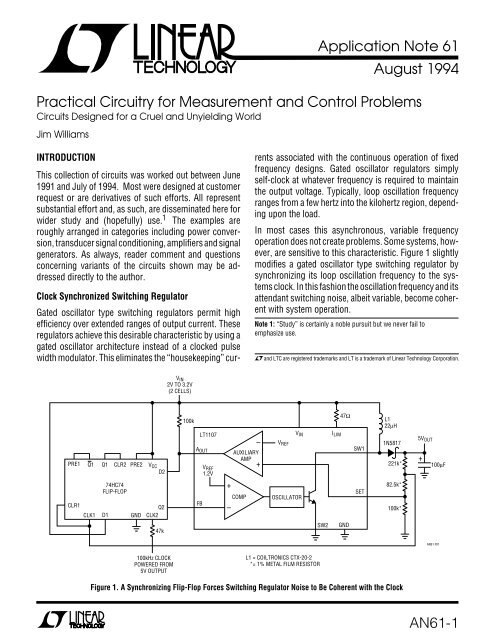
<strong>Application</strong> <strong>Note</strong> <strong>61</strong><strong>August</strong> <strong>1994</strong><strong>Practical</strong> <strong>Circuitry</strong> <strong>for</strong> Measurement and Control ProblemsCircuits Designed <strong>for</strong> a Cruel and Unyielding WorldJim WilliamsINTRODUCTIONThis collection of circuits was worked out between June1991 and July of <strong>1994</strong>. Most were designed at customerrequest or are derivatives of such ef<strong>for</strong>ts. All representsubstantial ef<strong>for</strong>t and, as such, are disseminated here <strong>for</strong>wider study and (hopefully) use. 1 The examples areroughly arranged in categories including power conversion,transducer signal conditioning, amplifiers and signalgenerators. As always, reader comment and questionsconcerning variants of the circuits shown may be addresseddirectly to the author.Clock Synchronized Switching RegulatorGated oscillator type switching regulators permit highefficiency over extended ranges of output current. Theseregulators achieve this desirable characteristic by using agated oscillator architecture instead of a clocked pulsewidth modulator. This eliminates the “housekeeping” currentsassociated with the continuous operation of fixedfrequency designs. Gated oscillator regulators simplyself-clock at whatever frequency is required to maintainthe output voltage. Typically, loop oscillation frequencyranges from a few hertz into the kilohertz region, dependingupon the load.In most cases this asynchronous, variable frequencyoperation does not create problems. Some systems, however,are sensitive to this characteristic. Figure 1 slightlymodifies a gated oscillator type switching regulator bysynchronizing its loop oscillation frequency to the systemsclock. In this fashion the oscillation frequency and itsattendant switching noise, albeit variable, become coherentwith system operation.<strong>Note</strong> 1: “Study” is certainly a noble pursuit but we never fail toemphasize use.and LTC are registered trademarks and LT is a trademark of Linear Technology Corporation.V IN 2V TO 3.2V(2 CELLS)PRE1Q1Q1CLR2PRE2V CCD2100kLT1107A OUTV REF 1.2V–AUXILIARYAMP+47ΩV REFV IN I LIMSW1L122µH1N5817221k*5V OUT+100µFCLR1CLK174HC74FLIP-FLOPD1GNDQ2CLK2FB+–COMPOSCILLATORSET82.5k*100k*47kSW2GND<strong>AN<strong>61</strong></strong> F01100kHz CLOCKPOWERED FROM5V OUTPUTL1 = COILTRONICS CTX-20-2*= 1% METAL FILM RESISTORFigure 1. A Synchronizing Flip-Flop Forces Switching Regulator Noise to Be Coherent with the Clock<strong>AN<strong>61</strong></strong>-1
<strong>Application</strong> <strong>Note</strong> <strong>61</strong>Circuit operation is best understood by temporarily ignoringthe flip-flop and assuming the LT1107 regulator’sA OUT and FB pins are connected. When the output voltagedecays the set pin drops below V REF , causing A OUT to fall.This causes the internal comparator to switch high, biasingthe oscillator and output transistor into conduction. L1receives pulsed drive, and its flyback events are depositedinto the 100µF capacitor via the diode, restoring outputvoltage. This overdrives the set pin, causing the IC toswitch off until another cycle is required. The frequency ofthis oscillatory cycle is load dependent and variable. If, asshown, a flip-flop is interposed in the A OUT -FB pin path,synchronization to a system clock results. When theoutput decays far enough (trace A, Figure 2) the A OUT pin(trace B) goes low. At the next clock pulse (trace C) theflip-flop Q2 output (trace D) sets low, biasing the comparator-oscillator.This turns on the power switch (V SWpin is trace E), which pulses L1. L1 responds in flybackfashion, depositing its energy into the output capacitor tomaintain output voltage. This operation is similar to thepreviously described case, except that the sequence is<strong>for</strong>ced to synchronize with the system clock by the flipflopsaction. Although the resulting loops oscillation frequencyis variable it, and all attendant switching noise, issynchronous and coherent with the system clock.A start-up sequence is required because this circuit’sclock is powered from its output. The start-up circuitrywas developed by Sean Gold and Steve Pietkiewicz of LTC.The flip-flop’s remaining section is connected as a buffer.The CLR1-CLK1 line monitors output voltage via theresistor string. When power is applied Q1 sets CLR2 low.This permits the LT1107 to switch, raising output voltage.When the output goes high enough Q1 sets CLR2 high andnormal loop operation commences.The circuit shown is a step-up type, although any switchingregulator configuration can utilize this synchronoustechnique.High Power 1.5V to 5V ConverterSome 1.5V powered systems (survival 2-way radios,remote, transducer-fed data acquisition systems, etc.)require much more power than stand-alone IC regulatorscan provide. Figure 3’s design supplies a 5V output with200mA capacity.The circuit is essentially a flyback regulator. The LT1170switching regulator’s low saturation losses and ease ofuse permit high power operation and design simplicity.Un<strong>for</strong>tunately this device has a 3V minimum supply requirement.Bootstrapping its supply pin from the 5Voutput is possible, but requires some <strong>for</strong>m of start-up+47µFV IN1.5V INL125µH1N58235V OUT200mA MAXV SW3.74k*+470µFA = 50mV/DIV(AC COUPLED)B = 5V/DIVC = 5V/DIVD = 5V/DIV+LT11701k6.8µFGNDV INFBSW1SENSELT10731k*240Ω*V CI LIMSW2GNDE = 5V/DIV<strong>AN<strong>61</strong></strong> F0320µs/DIV<strong>AN<strong>61</strong></strong> F02L1 = PULSE ENGINEERING #PE-92100* = 1% METAL FILM RESISTORFigure 2. Wave<strong>for</strong>ms <strong>for</strong> the Clock SynchronizedSwitching Regulator. Regulator Only Switches (Trace E)on Clock Transitions (Trace C), Resulting in ClockCoherent Output Noise (Trace A)Figure 3. 200mA Output 1.5V to 5V Converter. LowerVoltage LT1073 Provides Bootstrap Start-Up <strong>for</strong> LT1170High Power Switching Regulator<strong>AN<strong>61</strong></strong>-2
<strong>Application</strong> <strong>Note</strong> <strong>61</strong>mechanism. The 1.5V powered LT1073 switching regulator<strong>for</strong>ms a start-up loop. When power is applied theLT1073 runs, causing its V SW pin to periodically pullcurrent through L1. L1 responds with high voltage flybackevents. These events are rectified and stored in the 470µFcapacitor, producing the circuits DC output. The outputdivider string is set up so the LT1073 turns off when circuitoutput crosses about 4.5V. Under these conditions theLT1073 obviously can no longer drive L1, but the LT1170can. When the start-up circuit goes off, the LT1170 V IN pinhas adequate supply voltage and can operate. There issome overlap between start-up loop turn-off and LT1170turn-on, but it has no detrimental effect.The start-up loop must function over a wide range of loadsand battery voltages. Start-up currents approach 1A,necessitating attention to the LT1073’s saturation anddrive characteristics. The worst case is a nearly depletedbattery and heavy output loading.Figure 4 plots input-output characteristics <strong>for</strong> the circuit.<strong>Note</strong> that the circuit will start into all loads with V BAT =1.2V. Start-up is possible down to 1.0V at reduced loads.Once the circuit has started, the plot shows it will drive full200mA loads down to V BAT = 1.0V. Reduced drive ispossible down to V BAT = 0.6V (a very dead battery)! Figure5 graphs efficiency at two supply voltages over a range ofoutput currents. Per<strong>for</strong>mance is attractive, although atlower currents circuit quiescent power degrades efficiency.Fixed junction saturation losses are responsible<strong>for</strong> lower overall efficiency at the lower supply voltage.MINIMUM INPUT VOLTAGE TO MAINTAIN V OUT = 5V1.51.41.31.21.11.00.90.80.70.60.50.40.30.20.100STARTRUN20 40 60 80 100 120 140 160 180 200OUTPUT CURRENT (mA)<strong>AN<strong>61</strong></strong> F04Figure 4. Input-Output Data <strong>for</strong> the 1.5V to 5VConverter Shows Extremely Wide Start-Up andRunning Range into Full LoadEFFICIENCY (%)100908070605040302010V OUT = 5VV IN = 1.5VV IN = 1.2V00 20 40 60 80 100 120 140 160 180 200OUTPUT CURRENT (mA)<strong>AN<strong>61</strong></strong> F05Figure 5. Efficiency vs Operating Point <strong>for</strong> the 1.5V to5V Converter. Efficiency Suffers at Low Power Becauseof Relatively High Quiescent CurrentsLow Power 1.5V to 5V ConverterFigure 6, essentially the same approach as the precedingcircuit, was developed by Steve Pietkiewicz of LTC. It islimited to about 150mA output with commensurate restrictionson start-up current. It’s advantage, good efficiencyat relatively low output currents, derives from itslow quiescent power consumption.The LT1073 provides circuit start-up. When output voltage,sensed by the LT1073’s “set” input via the resistordivider, rises high enough Q1 turns on, enabling theLT1302. This device sees adequate operating voltage andresponds by driving the output to 5V, satisfying its feedbacknode. The 5V output also causes enough overdriveat the LT1073 feedback pin to shut the device down.Figure 7 shows maximum permissible load currents <strong>for</strong>start-up and running conditions. Per<strong>for</strong>mance is quitegood, although the circuit clearly cannot compete with theprevious design. The fundamental difference between thetwo circuits is the LT1170’s (Figure 3) much larger powerswitch, which is responsible <strong>for</strong> the higher available power.Figure 8, however, reveals another difference. The curvesshow that Figure 6 is significantly more efficient than theLT1170 based approach at output currents below 100mA.This highly desirable characteristic is due to the LT1302’smuch lower quiescent operating currents.<strong>AN<strong>61</strong></strong>-3
<strong>Application</strong> <strong>Note</strong> <strong>61</strong>L13.3µHD15V OUT10Ω100k1.5VCELL220ΩI LIM V INSETSW1LT1073FBA O+C147µF100kNCSWI LIMV INLT1302 SHDNQ12N390<strong>61</strong>00kFBV C100pFR1301k1%56.2k1%GNDSW2C2220µF+0.1µFPGNDGND0.01µF20k4.99k1%36.5k1%C1 = AVX TPSD476M016R0150C2 = AVX TPSE227M010R0100L1 = COILCRAFT DO3316-332D1 = MOTOROLA MBR3130LT3<strong>AN<strong>61</strong></strong> F06Figure 6. Single-Cell to 5V Converter Delivers 150mAwith Good Efficiency at Lower CurrentsMAXIMUM LOAD CURRENT (mA )10001001010.6RUNSTART0.8 1.0 1.2 1.4 1.6 1.8 2.0INPUT VOLTAGE (V)EFFICIENCY (%)727068666462605856545250481V IN = 1.5VV IN = 1.2V10 100 1000LOAD CURRENT (mA)<strong>AN<strong>61</strong></strong> F07<strong>AN<strong>61</strong></strong> F08Figure 7. Maximum Permissible Loads <strong>for</strong> Start-Upand Running Conditions. Allowable Load CurrentDuring Start-Up Is Substantially Less Than MaximumRunning Current.Figure 8. Efficiency Plot <strong>for</strong> Figure 6. Per<strong>for</strong>manceIs Better Than the Previous Circuit at LowerCurrents, Although Poorer at High Power<strong>AN<strong>61</strong></strong>-4
<strong>Application</strong> <strong>Note</strong> <strong>61</strong>Low Power, Low Voltage Cold Cathode FluorescentLamp Power SupplyMost Cold Cathode Fluorescent Lamp (CCFL) circuitsrequire an input supply of 5V to 30V and are optimized <strong>for</strong>bulb currents of 5mA or more. This precludes lower poweroperation from 2- or 3-cell batteries often used in palmtopcomputers and portable apparatus. A CCFL power supplythat operates from 2V to 6V is detailed in Figure 9. Thiscircuit, contributed by Steve Pietkiewicz of LTC, can drivea small CCFL over a 100µA to 2mA range.The circuit uses an LT1301 micropower DC/DC converterIC in conjunction with a current driven Royer class convertercomprised of T1, Q1 and Q2. When power andintensity adjust voltage are applied the LT1301’s I LIM pinis driven slightly positive, causing maximum switchingcurrent through the IC’s internal switch pin (SW). Currentflows from T1’s center tap, through the transistors, intoL1. L1’s current is deposited in switched fashion to groundby the regulator’s action.The Royer converter oscillates at a frequency primarily setby T1’s characteristics (including its load) and the 0.068µFcapacitor. LT1301 driven L1 sets the magnitude of theQ1-Q2 tail current, hence T1’s drive level. The 1N5817diode maintains L1’s current flow when the LT1301’sswitch is off. The 0.068µF capacitor combines with T1’scharacteristics to produce sine wave voltage drive at theQ1 and Q2 collectors. T1 furnishes voltage step-up andabout 1400Vp-p appears at its secondary. Alternatingcurrent flows through the 22pF capacitor into the lamp. Onpositive half-cycles the lamp’s current is steered to groundvia D1. On negative half-cycles the lamp’s current flowsthrough Q3’s collector and is filtered by C1. The LT1301’sI LIM pin acts as a 0V summing point with about 25µA biascurrent flowing out of the pin into C1. The LT1301 regulatesL1’s current to equalize Q3’s average collector current,representing 1/2 the lamp current, and R1’s current,represented by V A /R1. C1 smooths all current flow to DC.When V A is set to zero, the I LIM pin’s bias current <strong>for</strong>cesabout 100µA bulb current.TI9 722pF3kVV IN 2V TO 6V1 543 20.1µFNC1ΩV IN SELECTSENSESWLT1301SHDNGNDI LIMPGND +1N5817L147µH120ΩQ32N3904Q1ZTX8490.068µF+10µFQ2ZTX849CCFLC11µFR17.5K1%D11N4148<strong>AN<strong>61</strong></strong> F09SHUTDOWNT1 = COILTRONICS CTX110654-1L1 = COILCRAFT D03316-4730.68µF = WIMA MKP-20V A0V TO 5VDC IN INTENSITY ADJUST100µA TO 2mA BULB CURRENTFigure 9. Low Power Cold Cathode Fluorescent Lamp Supply Is Optimized <strong>for</strong> Low Voltage Inputs and Small Lamps<strong>AN<strong>61</strong></strong>-5
<strong>Application</strong> <strong>Note</strong> <strong>61</strong>Circuit efficiency ranges from 80% to 88% at full load,depending on line voltage. Current mode operation combinedwith the Royer’s consistent waveshape vs inputresults in excellent line rejection. The circuit has none ofthe line rejection problems attributable to the hystereticvoltage control loops typically found in low voltage micropowerDC/DC converters. This is an especially desirablecharacteristic <strong>for</strong> CCFL control, where lamp intensitymust remain constant with shifts in line voltage. Interactionbetween the Royer converter, the lamp and theregulation loop is far more complex than might be supposed,and subject to a variety of considerations. Fordetailed discussion see Reference 3.Low Voltage Powered LCD Contrast SupplyFigure 10, a companion to the CCFL power supply previouslydescribed, is a contrast supply <strong>for</strong> LCD panels. It wasdesigned by Steve Pietkiewicz of LTC. The circuit isnoteworthy because it operates from a 1.8V to 6V input,significantly lower than most designs. In operation theLT1300/LT1301 switching regulator drives T1 in flybackfashion, causing negative biased step-up at T1’s secondary.D1 provides rectification, and C1 smooths the outputto DC. The resistively divided output is compared to acommand input, which may be DC or PWM, by the IC’s“I LIM ” pin. The IC, <strong>for</strong>cing the loop to maintain 0V at theI LIM pin, regulates circuit output in proportion to thecommand input.Efficiency ranges from 77% to 83% as supply voltagevaries from 1.8V to 3V. At the same supply limits, availableoutput current increases from 12mA to 25mA.HeNe Laser Power SupplyHelium-Neon lasers, used <strong>for</strong> a variety of tasks, are difficultloads <strong>for</strong> a power supply. They typically need almost10kV to start conduction, although they require only about1500V to maintain conduction at their specified operatingcurrents. Powering a laser usually involves some <strong>for</strong>m ofstart-up circuitry to generate the initial breakdown voltageand a separate supply <strong>for</strong> sustaining conduction. Figure11’s circuit considerably simplifies driving the laser. TheV IN1.8V TO 6VT14CONTRAST OUTPUT VOUT –4V TO –29V17310 82150k+C122µF35V9D11N5819V INSW+NC100µFNCSENSELT1300ORLT1301SELECTSHDNI LIMSHUTDOWNPGNDGND12kT1 = DALE LPE-5047-AO4512k+2.2µFCOMMAND INPUTPWM OR DC0% TO 100%OR 0V TO 5V<strong>AN<strong>61</strong></strong> F10Figure 10. Liquid Crystal Display Contrast Supply Operates from 1.8V to 6V with –4V to – 29V Output Range<strong>AN<strong>61</strong></strong>-6
<strong>Application</strong> <strong>Note</strong> <strong>61</strong>start-up and sustaining functions have been combinedinto a single, closed-loop current source with over 10kV ofcompliance. The circuit is recognizable as a reworkedCCFL power supply with a voltage tripled DC output. 2When power is applied, the laser does not conduct and thevoltage across the 190Ω resistor is zero. The LT1170switching regulator FB pin sees no feedback voltage, andits switch pin (V SW ) provides full duty cycle pulse widthmodulation to L2. Current flows from L1’s center tapthrough Q1 and Q2 into L2 and the LT1170. This currentflow causes Q1 and Q2 to switch, alternately driving L1.The 0.47µF capacitor resonates with L1, providing boostedsine wave drive. L1 provides substantial step-up, causingabout 3500V to appear at its secondary. The capacitorsand diodes associated with L1’s secondary <strong>for</strong>m a voltagetripler, producing over 10kV across the laser. The laserbreaks down and current begins to flow through it. The 47kresistor limits current and isolates the laser’s load characteristic.The current flow causes a voltage to appear acrossthe 190Ω resistor. A filtered version of this voltage appearsat the LT1170 FB pin, closing a control loop. TheLT1170 adjusts pulse width drive to L2 to maintain the FBpin at 1.23V, regardless of changes in operating conditions.In this fashion, the laser sees constant current drive,<strong>Note</strong> 2: See References 2 and 3 and this text’s Figure 9.0.01µF5kV1800pF10kV47k5W1800pF10kVL111 8 HV DIODES5 4 1 32V IN9V TO 35V+150Ω2.2µF0.47µF+V SW 10k2.2µFQ1Q2L2MUR405145µHV IN FBLT11700.1µFV C GND+10k10µFV IN1N4002(ALL)190Ω1%LASERHV DIODES =SEMTECH-FM-500.47µF =WIMA 3× 0.15µF TYPE MKP-20Q1, Q2 =ZETEX ZTX849L1 =COILTRONICS CTX02-11128-2L2 =PULSE ENGINEERING PE-92105LASER =HUGHES 3121H-P<strong>AN<strong>61</strong></strong> F11Figure 11. LASER Power Supply Is Essentially A 10,000V Compliance Current Source<strong>AN<strong>61</strong></strong>-7
<strong>Application</strong> <strong>Note</strong> <strong>61</strong>in this case 6.5mA. Other currents are obtainable byvarying the 190Ω value. The 1N4002 diode string clampsexcessive voltages when laser conduction first begins,protecting the LT1170. The 10µF capacitor at the V C pinfrequency compensates the loop and the MUR405 maintainsL1’s current flow when the LT1170 V SW pin is notconducting. The circuit will start and run the laser over a9V to 35V input range with an electrical efficiency of about80%.Compact Electroluminescent Panel Power SupplyElectroluminescent (EL) panel LCD backlighting presentsan attractive alternative to fluorescent tube (CCFL) backlightingin some portable systems. EL panels are thin,lightweight, lower power, require no diffuser and work atlower voltage than CCFLs. Un<strong>for</strong>tunately, most EL DC/ACinverters use a large trans<strong>for</strong>mer to generate the 400Hz95V square wave required to drive the panel. Figure 12’scircuit, developed by Steve Pietkiewicz of LTC, eliminatesthe trans<strong>for</strong>mer by employing an LT1108 micropowerDC/DC converter IC. The device generates a 95VDC potentialvia L1 and the diode-capacitor doubler network. Thetransistors switch the EL panel between 95V and ground.C1 blocks DC and R1 allows intensity adjustment. The400Hz square wave drive signal can be supplied by themicroprocessor or a simple multivibrator. When comparedto conventional EL panel supplies, this circuit isnoteworthy because it can be built in a square inch with a0.5 inch height restriction. Additionally, all componentsare surface mount types, and the usual large and heavy400Hz trans<strong>for</strong>mer is eliminated.0.1µF100V95VV IN 2V TO 12V33pF+I LIM47ΩV INL1100µH+0.1µF100V1MMMBTA42MMBTA42C11µF100VU1LT1108CS8SW1FB2.26MMMBTA92ELPANELGNDSW2R125k30.1k0.47µF200VMMBTA4210k400Hz DRIVESQUARE WAVE= MOTOROLA MURS120T3L1 = COILCRAFT DO3316-104<strong>AN<strong>61</strong></strong> F12Figure 12. Switch Mode EL Panel Driver Eliminates Large 400Hz Trans<strong>for</strong>mer<strong>AN<strong>61</strong></strong>-8
<strong>Application</strong> <strong>Note</strong> <strong>61</strong>3.3V Powered Barometric Pressure SignalConditionerThe move to 3.3V digital supply voltage creates problems<strong>for</strong> analog signal conditioning. In particular, transducerbased circuits often require higher voltage <strong>for</strong> propertransducer excitation. DC/DC converters in standard configurationscan address this issue but increase powerconsumption. Figure 13’s circuit shows a way to provideproper transducer excitation <strong>for</strong> a barometric pressuresensor while minimizing power requirements.The 6kΩ transducer T1 requires precisely 1.5mA of excitation,necessitating a relatively high voltage drive. A1senses T1’s current by monitoring the voltage drop acrossthe resistor string in T1’s return path.A1’s output biases the LT1172 switching regulator’s operatingpoint, producing a stepped up DC voltage whichappears as T1’s drive and A2’s supply voltage. T1’s returncurrent out of pin 6 closes a loop back at A1 which is slavedto the 1.2V reference. This arrangement provides therequired high voltage drive (≈10V) while minimizing powerconsumption. This is so because the switching regulatorproduces only enough voltage to satisfy T1’s currentrequirements. Instrumentation amplifier A2 and A3 providegain and LTC1287 A/D converter gives a 12-bit digitaloutput. A2 is bootstrapped off the transducer supply,enabling it to accept T1’s common-mode voltage. Circuitcurrent consumption is about 14mA. If the shutdown pinis driven high the switching regulator turns off, reducingT1PRESSURETRANSDUCER5≈ 10V DURING OPERATIONTO PROCESSOR3.3V10641µF–A2LT1101+A = 10+3.3VA31/2 LT1078–0.05µF10k*1N7525.6VCLK D OUTCS+IN LTC1287 V CC–INGND V REFBRIDGECURRENTTRIM700Ω*50Ω1µF1MCALIB+3.3V22µFMUR1103.3VL1150µH1N4148BRIDGECURRENTMONITOR(0.1500V)100Ω**100k–A11/2 LT1078+1N41482.2µF+V CV INE1LT1172E2V SWGNDFBNC* = 1% FILM RESISTOR** = 0.1% FILM RESISTORL1 = TOKO 262-LYF-0095KT1 = NOVASENSOR (FREMONT, CA)NPH-8-100AHLT10341.2V10k2N3904100kSHUTDOWN3.3V<strong>AN<strong>61</strong></strong> F13Figure 13. 3.3V Powered, Digital Output, Barometric Pressure Signal Conditioner<strong>AN<strong>61</strong></strong>-9
<strong>Application</strong> <strong>Note</strong> <strong>61</strong>total power consumption to about 1mA. In shutdown the3.3V powered A/D’s output data remains valid. In practice,the circuit provides a 12-bit representation of ambientbarometric pressure after calibration. To calibrate, adjustthe “bridge current trim” <strong>for</strong> exactly 0.1500V at theindicated point. This sets T1’s current to the manufacturersspecified point. Next, adjust A3’s trim so that the digitaloutput corresponds to the known ambient barometricpressure. If a pressure standard is not available thetransducer is supplied with individual calibration data,permitting circuit calibration.Some applications may require operation over a widersupply range and/or a calibrated analog output. Figure14’s circuit is quite similar, except that the A/D converteris eliminated and a 2.7V to 7V supply is acceptable. Thecalibration procedure is identical, except that A3’s analogoutput is monitored.Single Cell BarometersIt is possible to power these circuits from a single cellwithout sacrificing per<strong>for</strong>mance. Figure 15, a direct extensionof the above approaches, simply substitutes a switchingregulator that will run from a single 1.5V battery. Inother respects loop action is nearly identical.Figure 16, also a 1.5V powered design, is related buteliminates the instrumentation amplifier. As be<strong>for</strong>e, the6kΩ transducer T1 requires precisely 1.5mA of excitation,necessitating a relatively high voltage drive. A1’s positiveinput senses T1’s current by monitoring the voltage dropacross the resistor string in T1’s return path. A1’s negativeinput is fixed by the 1.2V LT1004 reference. A1’s outputbiases the 1.5V powered LT1110 switching regulator. TheLT1110’s switching produces two outputs from L1. Pin4’s rectified and filtered output powers A1 and T1. A1’s510T164–A2LT1101+A = 10+A31/2 LT1078–20k*OUTPUT0V TO 3.100V =0 TO 31.00" Hg.1.500mA10k*+22µF3.3VBRIDGECURRENTTRIM700Ω*50Ω1µFOUTPUTTRIM1k3.3VMUR110L1150µH100Ω0.1%* = 1% FILM RESISTORL1 = TOKO 262-LYF-0095KT1 = NOVASENSOR NPH-8-100AH100k–A11/2 LT1078+10k3.3V2.2µF1N4148+V CV INE1V SWLT1172 FBE2 GNDNCLT10341.2V<strong>AN<strong>61</strong></strong> F13Figure 14. Single Supply Barometric Pressure Signal Conditioner Operates Over a 2.7V to 7V Range<strong>AN<strong>61</strong></strong>-10
<strong>Application</strong> <strong>Note</strong> <strong>61</strong>A1T168kNOVASENSOR5+NPH-8-100AH †1041µFNON-POLAR–A2LT10770.1µF 200k*1% 10k1%OUTPUT6+0.1µF100k100µF2 1+3 L1 4698Ω1%R1**50Ω100Ω0.1%–100kA1LT10771N4148100kAA CELL+1µF6I LSW1V IN8 3FBLT1110AOSETSW2GND150Ω2 15 47LT1004-1.2* = NOMINAL VALUE. EACH SENSOR REQUIRES SELECTION** = TRIM FOR 150mV ACROSS A1-A2†= LUCAS NOVASENSOR FREMONT, CA (510) 490-9100L1 = COILTRONICS CTX50-1R21k0V TO 3.100V =0 TO 31.00"Hg.100Ω1N41481N5818430k39k100Ω+ 390µF16VNICHICONPL<strong>AN<strong>61</strong></strong> F16Figure 16. 1.5V Powered Barometric Pressure Signal Conditioner Floats Bridge Drive toEliminate Instrumentation Amplifier. Voltage Boosted Current Loop Drives TransducerA2<strong>AN<strong>61</strong></strong>-12
<strong>Application</strong> <strong>Note</strong> <strong>61</strong>Until recently, this type of accuracy and stability has onlybeen attainable with bonded strain gauge and capacitivelybasedtransducers, which are quite expensive. As such,semiconductor pressure transducer manufacturers whoseproducts per<strong>for</strong>m at the levels reported are to be applauded.Although high quality semiconductor transducersare still not comparable to more mature technologies,their cost is low and they are vastly improved over earlierdevices.The circuit pulls 14mA from the battery, allowing about250 hours operation from one D cell.Quartz Crystal-Based ThermometerAlthough quartz crystals have been utilized as temperaturesensors (see Reference 5), there has been almost nowidespread adaptation of this technology. This is primarilydue to the lack of standard product quartz-based temperaturesensors. The advantages of quartz-based sensorsinclude simple signal conditioning, good stability and adirect, noise immune digital output almost ideally suited toremote sensing.Figure 17 utilizes an economical, commercially available(see Reference 6) quartz-based temperature sensor in athermometer scheme suited to remote data collection.10pF<strong>61</strong>0M4 LTC4858 2 3 751NC 5VY1+33.5ppm/°C100k1000 FEET TWISTED-PAIR15pF5V86OUTLTC485 174100Ω 35 NC20°C TO 100°C = 2<strong>61</strong>.900kHz – 262.800kHzY1 = MICRO CRYSTAL (SWISS) MT1/33.5ppm/°C0°C = 2<strong>61</strong>.900kHz100°C = 262.800kHzFigure 17. Quartz Crystal Based Circuit ProvidesTemperature-to-Frequency Conversion. RS485Transceivers Allow Remote Sensing<strong>AN<strong>61</strong></strong> • F17The LTC485 RS485 transceiver is set up in the transmitmode. The crystal and discrete components combine withthe IC’s inverting gain to <strong>for</strong>m a Pierce type oscillator. TheLTC485’s differential line driving outputs provide frequencycoded temperature data to a 1000-foot cable run.A second RS485 transceiver differentially receives thedata and presents a single-ended output. Accuracy dependson the grade of quartz sensor specified, with 1°Cover 0°C to 100°C achievable.Ultra-Low Noise and Low Drift Chopped-FET AmplifierFigure 18’s circuit combines the extremely low drift of achopper-stabilized amplifier with a pair of low noise FETs.The result is an amplifier with 0.05µV/°C drift, offset within5µV, 100pA bias current and 50nV noise in a 0.1Hz to 10Hzbandwidth. The noise per<strong>for</strong>mance is especially noteworthy;it is almost 35 times better than monolithic chopperstabilizedamplifiers and equals the best bipolar types.FETs Q1 and Q2 differentially feed A2 to <strong>for</strong>m a simple lownoise op amp. Feedback, provided by R1 and R2, setsclosed-loop gain (in this case 10,000) in the usual fashion.Although Q1 and Q2 have extraordinarily low noise characteristics,their offset and drift are uncontrolled. A1, achopper-stabilized amplifier, corrects these deficiencies.It does this by measuring the difference between theamplifier’s inputs and adjusting Q1’s channel current viaQ3 to minimize the difference. Q1’s skewed drain valuesensure that A1 will be able to capture the offset. A1 and Q3supply whatever current is required into Q1’s channel to<strong>for</strong>ce offset within 5µV. Additionally, A1’s low bias currentdoes not appreciably add to the overall 100pA amplifierbias current. As shown, the amplifier is set up <strong>for</strong> anoninverting gain of 10,000 although other gains andinverting operation are possible. Figure 19 is a plot of themeasured noise per<strong>for</strong>mance.The FETs’ V GS can vary over a 4:1 range. Because of this,they must be selected <strong>for</strong> 10% V GS matching. This matchingallows A1 to capture the offset without introducing anysignificant noise.<strong>AN<strong>61</strong></strong>-13
<strong>Application</strong> <strong>Note</strong> <strong>61</strong>15V0.02µF+A1LTC1150––15V10kQ32N2907–15V1k* 200Ω*15V0.02µF450Ω* 900Ω*100k100k–A2LT1097+5OUTPUT+ INPUTQ1Q2OPTIONALOVERCOMPENSATIONR1100k* = 1% FILM RESISTORQ1, Q2 = 2SK147 TOSHIBA750Ω*– INPUTR210Ω–15V<strong>AN<strong>61</strong></strong> F18Figure 18. Chopper-Stabilized FET Pair Combines Low Bias, Offset and Drift with 45nV Noise200NANOVOLTS<strong>AN<strong>61</strong></strong> F1910 SECONDSFigure 19. Figure 18’s 45nV Noise Per<strong>for</strong>mance in a 0.1Hz to 10Hz Bandwidth.A1’s Low Offset and Drift Are Retained, But Noise Is Almost 35 Times Better<strong>AN<strong>61</strong></strong>-14
<strong>Application</strong> <strong>Note</strong> <strong>61</strong>Figure 20 shows the response (trace B) to a 1mV inputstep (trace A). The output is clean, with no overshoots oruncontrolled components. If A2 is replaced with a fasterdevice (e.g., LT1055) speed increases by an order ofmagnitude with similar damping. A2’s optional overcompensationcan be used (capacitor to ground) to optimizeresponse <strong>for</strong> low closed-loop gains.A = 500µV/DIVB = 5V/DIV100µs/DIV<strong>AN<strong>61</strong></strong> F20Figure 20. Step Response <strong>for</strong> the Low Noise × 10,000Amplifier. A 10× Speed Increase Is Obtainable byReplacing A2 with a Faster DeviceHigh Speed Adaptive Trigger CircuitLine receivers often require an adaptive trigger to compensate<strong>for</strong> variations in signal amplitude and DC offsets. Thecircuit in Figure 21 triggers on 2mV to 100mV signals from100Hz to 10MHz while operating from a single 5V rail. A1,operating at a gain of 20, provides wideband AC gain. Theoutput of this stage biases a 2-way peak detector (Q1-Q4).The maximum peak is stored in Q2’s emitter capacitor,while the minimum excursion is retained in Q4’s emittercapacitor. The DC value of A1’s output signal’s midpointappears at the junction of the 500pF capacitor and the10MΩ units. This point always sits midway between thesignal’s excursions, regardless of absolute amplitude.This signal-adaptive voltage is buffered by A2 to set thetrigger voltage at the LT1116’s positive input. The LT1116’snegative input is biased directly from A1’s output. TheLT1116’s output, the circuit’s output, is unaffected by 50:1signal amplitude variations. Bandwidth limiting in A1 doesnot affect triggering because the adaptive trigger thresholdvaries ratiometrically to maintain circuit output.Split supply versions of this circuit can achieve bandwidthsto 50MHz with wider input operating range (SeeReference 7).5V3k5VQ1Q25V2k750Ω+A1LT1192–1kQ30.005µF0.005µFQ4500pF3M3M+–5VA2LT1006+10µFINPUT0.01µF+50ΩC1100µFC20.1µFNPN = 2N3904PNP = 2N39063k500Ω1N41481N4148500Ω0.1µF+–5VLT1116QQTRIGGEROUT<strong>AN<strong>61</strong></strong> F21Figure 21. Fast Single Supply Adaptive Trigger. Output Comparator’s Trip Level Varies Ratiometricallywith Input Amplitude, Maintaining Data Integrity Over 50:1 Input Amplitude Range<strong>AN<strong>61</strong></strong>-15
<strong>Application</strong> <strong>Note</strong> <strong>61</strong>Wideband, Thermally-Based RMS/DC Converter<strong>Application</strong>s such as wideband RMS voltmeters, RF levelingloops, wideband AGC, high crest factor measurements,SCR power monitoring and high frequency noisemeasurements require wideband, true RMS/DC conversion.The thermal conversion method achieves vastlyhigher bandwidth than any other approach. ThermalRMS/DC converters are direct acting, thermoelectronicanalog computers. The thermal technique is explicit, relyingon “first principles,” e.g,. a wave<strong>for</strong>ms RMS value isdefined as its heating value in a load.Figure 22 is a wideband, thermally-based RMS/DC converter.3 It provides a true RMS/DC conversion from DC to10MHz with less than 1% error, regardless of input signalwaveshape. It also features high input impedance andoverload protection.The circuit consists of three blocks; a wideband FET inputamplifier, the RMS/DC converter and overload protection.The amplifier provides high input impedance, gain anddrives the RMS/DC converters input heater. Input resistanceis defined by the 1M resistor with input capacitanceabout 3pF. Q1 and Q2 constitute a simple, high speed FETinput buffer. Q1 functions as a source follower, with the Q2current source load setting the drain-source channel current.The LT1206 provides a flat 10MHz bandwidth gain often. Normally, this open-loop configuration would be quitedrifty because there is no DC feedback. The LT1097contributes this function to stabilize the circuit. It does thisby comparing the filtered circuit output to a similarlyfiltered version of the input signal. The amplified differencebetween these signals is used to set Q2’s bias, andhence Q1’s channel current. This <strong>for</strong>ces Q1’s V GS towhatever voltage is required to match the circuit’s inputand output potentials. The capacitor at A1 provides stableloop compensation. The RC network in A1’s output preventsit from seeing high speed edges coupled throughQ2’s collector-base junction. Q4, Q5 and Q6 <strong>for</strong>m a lowleakage clamp which precludes A1 loop latch-up duringstart-up or overdrive conditions. This can occur if Q1 ever<strong>for</strong>ward biases. The 5K-50pF network gives A2 a slightpeaking characteristic at the highest frequencies, allowing1% flatness to 10MHz. A2’s output drives the RMS/DCconverter.The LT1088 based RMS/DC converter is made up ofmatched pairs of heaters and diodes and a control amplifier.The LT1206 drives R1, producing heat which lowersD1’s voltage. Differentially connected A3 responds bydriving R2, via Q3, to heat D2, closing a loop around theamplifier. Because the diodes and heater resistors arematched, A3’s DC output is related to the RMS value of theinput, regardless of input frequency or waveshape. Inpractice, residual LT1088 mismatches necessitate a gaintrim, which is implemented at A4. A4’s output is the circuitoutput. The LT1004 and associated components frequencycompensate the loop and provide good settlingtime over wide ranges of operating conditions (see Footnote3).Start-up or input overdrive can cause A2 to deliver excessivecurrent to the LT1088 with resultant damage. C1 andC2 prevent this. Overdrive <strong>for</strong>ces D1’s voltage to anabnormally low potential. C1 triggers low under theseconditions, pulling C2’s input low. This causes C2’s outputto go high, putting A2 into shutdown and terminating theoverload. After a time determined by the RC at C2’s input,A2 will be enabled. If the overload condition still exists theloop will almost immediately shut A2 down again. Thisoscillatory action will continue, protecting the LT1088until the overload condition is removed.<strong>Note</strong> 3: Thermally based RMS/DC conversion is detailed in Reference 9.<strong>AN<strong>61</strong></strong>-16
–+<strong>Application</strong> <strong>Note</strong> <strong>61</strong>0.022µF1.5M 1k3300pF0 – 1V RMS DC –10MHz 15V1MQ22N3904330Ω–15VQ12N54863k330pF10MA1LT10970.0110k10M0.110MHzTRIM5k+–50pFA2LT1206SD 900Ω*100Ω*ZERO TRIM(TRIM AT 10% OFFULL-SCALE)0.01µF3 250Ω250Ω 10R1 R272.7k*12 5LT1088D115V500Ω2.7k*D21k*1k*0.01µF–+9.09M*10kFULL-SCALETRIM15VA31/2 LT1013+–9.09M*LT1004-1.2V1kQ32N2219A41/2 LT10133k10k*VOUT10k*14Q4 0.1–15V0.1µF113 6 8Q52N3904s* = 1% FILM RESISTORQ6OVERLOAD TRIM. SET AT10% BELOW D1's VOLTAGEWITH CIRCUIT OPERATINGAT FULL SCALE+–15VC11/2 LT101810k15V15V2k1k 510k1N914LT10041.2V15V0.110k–+–15VC21/2 LT10184.7k15V24k<strong>AN<strong>61</strong></strong> F2215VFigure 22. Complete 10MHz Thermally-Based RMS/DC Converter Has 1% Accuracy, High Input Impedance and Overload Protection<strong>AN<strong>61</strong></strong>-17
<strong>Application</strong> <strong>Note</strong> <strong>61</strong>Per<strong>for</strong>mance <strong>for</strong> the circuit is quite impressive. Figure 23plots error from DC to 11MHz. The graph shows 1% errorbandwidth of 11MHz. The slight peaking out to 5MHz isdue to the gain boost network at A2’s negative input. Thepeaking is minimal compared to the total error envelope,and a small price to pay to get the 1% accuracy to 10MHz.To trim this circuit put the 5kΩ potentiometer at itsmaximum resistance position and apply a 100 mV, 5MHzsignal. Trim the 500Ω adjustment <strong>for</strong> exactly 1V OUT . Next,apply a 5MHz 1V input and trim the 10k potentiometer <strong>for</strong>10.00V OUT . Finally, put in 1V at 10MHz and adjust the 5kΩtrimmer <strong>for</strong> 10.00V OUT . Repeat this sequence until circuitoutput is within 1% accuracy <strong>for</strong> DC-10MHz inputs. Twopasses should be sufficient.It is worth considering that this circuit per<strong>for</strong>ms the samefunction as instruments costing thousands of dollars. 4ERROR (%)10–1010.7% ERROR AT 10MHz2 3 4 5 6 7 8 9 10 11FREQUENCY (MHz)<strong>AN<strong>61</strong></strong> F23Figure 23. Error Plot <strong>for</strong> the RMS/DC Converter.Frequency Dependent Gain Boost at A2 Preserves 1%Accuracy, But Causes Slight Peaking Be<strong>for</strong>e Roll-OffHall Effect Stabilized Current Trans<strong>for</strong>merCurrent trans<strong>for</strong>mers are common and convenient. Theypermit wideband current measurement independent ofcommon-mode voltage considerations. The most conve-nient current trans<strong>for</strong>mers are the “clip-on” type, commerciallysold as “current probes.” A problem with allsimple current trans<strong>for</strong>mers is that they cannot sense DCand low frequency in<strong>for</strong>mation. This problem was addressedin the mid-1960’s with the advent of the Hall effectstabilized current probe. This approach uses a Hall effectdevice within the trans<strong>for</strong>mer core to sense DC and lowfrequency signals. This in<strong>for</strong>mation is combined with thecurrent trans<strong>for</strong>mers output to <strong>for</strong>m a composite DC-tohighfrequency output. Careful roll-off and gain matchingof the two channels preserves amplitude accuracy at allfrequencies. 5 Additionally, the low frequency channel isoperated as a “<strong>for</strong>ce-balance,” meaning that the lowfrequency amplifier’s output is fed back to magneticallybias the trans<strong>for</strong>mer flux to zero. Thus, the Hall effectdevice does not have to respond linearly over wide rangesof current and the trans<strong>for</strong>mer core never sees DC bias,both advantageous conditions. The amount of DC and lowfrequency in<strong>for</strong>mation is obtained at the amplifier’s output,which corresponds to the bias needed to offset themeasured current.Figure 24 shows a practical circuit. The Hall effect transducerlies within the core of the clip-on current trans<strong>for</strong>merspecified. A very simplistic way to model the Hallgenerator is as a bridge, excited by the two <strong>61</strong>9Ω resistors.The Hall generator’s outputs (the midpoints of the“bridge”) feed differential input transconductance amplifierA1, which takes gain, with roll-off set by the 50Ω,0.02µF RC at its output. Further gain is provided by A2, inthe same package as A1. A current buffer provides powergain to drive the current trans<strong>for</strong>mers secondary. Thisconnection closes a flux nulling loop in the transducercore. The offset adjustments should be set <strong>for</strong> 0V outputwith no current flowing in the clip-on transducer. Similarly,the loop gain and bandwidth trims should be set sothat the composite output (the combined high and lowfrequency output across the grounded 50Ω resistor) hasclean step response and correct amplitude from DC tohigh frequency.<strong>Note</strong> 4: Viewed from a historical perspective it is remarkable that so muchprecision wideband per<strong>for</strong>mance is available from such a relatively simpleconfiguration. For perspective, see Appendix A, “Precision Wideband<strong>Circuitry</strong> . . . Then and Now.”<strong>Note</strong> 5: Details of this scheme are nicely presented in Reference 15.Additional relevant commentary on parallel path schemes appears inReference 7.<strong>AN<strong>61</strong></strong>-18
<strong>Application</strong> <strong>Note</strong> <strong>61</strong>+16V<strong>61</strong>9Ω(TYPICAL)DC AND LOW FREQUENCY OUTPUTCONCEPTUAL MODELOF HALL EFFECTSENSOR-XFORMER.TEKTRONIX120-0464-00 OR120-0464-02CURRENTCARRYINGCONDUCTORANDRESULTANTFIELD–16V<strong>61</strong>9Ω(TYPICAL)10µH10µH32+DIFFERENTIALHALL SENSORAMPLIFIER+16V7A1OTALT1228–I5 SET+16V2k1k50Ω50ΩBANDWIDTH0.02(TYPICAL)1kOFFSETTRIMCOMPOSITE OUTPUT TO OPTIONALATTENUATOR AND WIDEBAND AMPLIFIER1k100ΩOFFSETADJ.330Ω1kOFFSETTRIM1+A2CFA8 LT1228–41k–16–16V6200Ω20kLOOP GAIN4.7k16ΩX1CURRENT BUFFERA1, A2 = LT1228 DUALAN62 TA24Figure 24. Hall Effect Stabilized Current Trans<strong>for</strong>mer (DC → High Frequency Current Probe)Figure 25 shows a practical way to conveniently evaluatethis circuits per<strong>for</strong>mance. This partial schematic of theTektronix P-6042 current probe shows a similar signalconditioning scheme <strong>for</strong> the transducer specified in Figure24. In this case Q22, Q24 and Q29 combine with differentialstage M-18 to <strong>for</strong>m the Hall amplifier. To evaluateFigure 24’s circuit remove M-18, Q22, Q24 and Q29. Next,connect LT1228 pins 3 and 2 to the <strong>for</strong>mer M-18 pins 2and 10 points, respectively. The ±16V supplies are availablefrom the P-6042’s power bus. Also, connect the rightend of Figure 24’s 200Ω resistor to what was Q29’scollector node. Finally, per<strong>for</strong>m the offset, loop gain andbandwidth trims as previously described.<strong>AN<strong>61</strong></strong>-19
<strong>Application</strong> <strong>Note</strong> <strong>61</strong>Figure reproduced with permissionof Tektronix, Inc.Figure 25. Tektronix P-6042 Hall Effect Based Current Probe Servo Loop.Figure 24 Replaces M18 Amplifier and Q22, Q24 and Q29TOWIDEBANDAMPLIFIERSECTION<strong>AN<strong>61</strong></strong> F25<strong>AN<strong>61</strong></strong>-20
<strong>Application</strong> <strong>Note</strong> <strong>61</strong>Triggered 250 Picosecond Rise Time Pulse GeneratorVerifying the rise time limit of wideband test equipmentsetups is a difficult task. In particular, the “end-to-end”rise time of oscilloscope-probe combinations is oftenrequired to assure measurement integrity. Conceptually, apulse generator with rise times substantially faster thanthe oscilloscope-probe combination can provide this in<strong>for</strong>mation.Figure 26’s circuit does this, providing an800ps pulse with rise and fall times inside 250ps. Pulseamplitude is 10V with a 50Ω source impedance. Thiscircuit has similarities to a previously published design(see Reference 7) except that it is triggered instead of freerunning. This feature permits synchronization to a clock orother event. The output phase with respect to the triggeris variable from 200ps to 5ns.The pulse generator requires high voltage bias <strong>for</strong> operation.The LT1182 switching regulator to <strong>for</strong>ms a highvoltage switched mode control loop. The LT1182 pulse+1µF500kAVALANCHE BIASBIAS ADJUSTV IN V SWTYPICALLY 70V.(SEE TEXT)FBE2R3LT118212k1ME1GND V CTRIGGER INPUTT RISE = 10NS ORLESS. 1V TO 5V(SEE TEXT)50kHz MAXIMUM+5VL1820µHMUR120L22µFC23pF TO 12pF430kFigure 26. Triggered 250ps Rise Time Pulse Generator.Trigger Pulse Amplitude Controls Output Phase+50ΩL1 = J.W. MILLER # 100267L2 = 1 TURN # 28 WIRE, 1/4" TOTAL LENGTH5pF2µF10k10k+R450Ω1µFC12pFQ12N2369 (SEE TEXT)OUTPUTAN62 F26width modulates at its 100kHz clock rate. L1’s inductiveevents are rectified and stored in the 2µF output capacitor.The adjustable resistor divider provides feedback to theLT1182. The 10k-1µF RC provides noise filtering.The high voltage is applied to Q1, a 40V breakdown device,via the R3-C1 combination. The high voltage “bias adjust”control should be set at the point where free runningpulses across R4 just disappear. This puts Q1 slightlybelow its avalanche point. When an input trigger pulse isapplied Q1 avalanches. The result is a quickly rising, veryfast pulse across R4. C1 discharges, Q1’s collector voltagefalls and breakdown ceases. C1 then recharges to justbelow the avalanche point. At the next trigger pulse thisaction repeats. 6Figure 27 shows wave<strong>for</strong>ms. A 3.9GHz sampling oscilloscope(Tektronix 6<strong>61</strong> with 4S2 sampling pug-in) measuresthe pulse (trace B) at 10V high with an 800ps base.Rise time is 250ps, with fall time indicating 200ps. Thetimes are probably slightly faster, as the oscilloscope’s90ps rise time influences the measurement. 7 The inputtrigger pulse is trace A. Its amplitude provides a convenientway to vary the delay time between the trigger andoutput pulses. A 1V to 5V amplitude setting produces acontinuous 5ns to 200ps delay range.A = 0.5V/DIVB = 1V/DIV(UNCALIBRATED)100 PICOSECONDS/DIV<strong>AN<strong>61</strong></strong> F27Figure 27. Input Pulse Edge (Trace A) Triggers theAvalanche Pulse Output (Trace B). Display Granularity IsCharacteristic of Sampling Oscilloscope Operation<strong>Note</strong> 6: This circuit is based on the operation of the Tektronix Type 111Pulse Generator. See Reference 16.<strong>Note</strong> 7: I’m sorry, but 3.9GHz is the fastest ’scope in my house (as ofSeptember, 1993).<strong>AN<strong>61</strong></strong>-21
<strong>Application</strong> <strong>Note</strong> <strong>61</strong>Some special considerations are required to optimizecircuit per<strong>for</strong>mance. L2’s very small inductance combineswith C2 to slightly retard the trigger pulse’s rise time. Thisprevents significant trigger pulse artifacts from appearingat the circuit’s output. C2 should be adjusted <strong>for</strong> the bestcompromise between output pulse rise time and purity.Figure 28 shows partial pulse rise with C2 properly adjusted.There are no discernible discontinuities related tothe trigger event.mandate a separate 12V supply and pulse <strong>for</strong>ming circuitry.Figure 29’s circuit provides the complete flashmemory programming function with a single IC and somediscrete components. All components are surface mounttypes, so little board space is required. The entire functionruns off a single 5V supply.L133µHMBRS130T3(MOTOROLA)5VSWITCHV INLT1109-12SHDN SENSEGND33µF+VPP FLASH V OUT 12V60mA0.2V/DIV1 = FLASH PROGRAM0 = STANDBYL1 = SUMIDA CD54-330<strong>AN<strong>61</strong></strong> • F29Figure 29. Switching Regulator Provides CompleteFlash Memory Programmer500 PICOSECONDS/DIV<strong>AN<strong>61</strong></strong> F28Figure 28. Expanded Scale View of Leading Edge IsClean with No Trigger Pulse Artifacts. DisplayGranularity Derives from Sampling OscilloscopeOperationQ1 may require selection to get avalanche behavior. Suchbehavior, while characteristic of the device specified, isnot guaranteed by the manufacturer. A sample of 50Motorola 2N2369s, spread over a 12 year date code span,yielded 82%. All “good” devices switched in less than600ps. C1 is selected <strong>for</strong> a 10V amplitude output. Valuespread is typically 2pF to 4pF. Ground plane type constructionwith high speed layout, connection and terminationtechniques are essential <strong>for</strong> a good results from this circuit.Flash Memory ProgrammerAlthough “Flash” type memory is increasingly popular, itdoes require some special programming features. The 5Vpowered memories need a carefully controlled 12V “VPP”programming pulse. The pulse’s amplitude must be within5% to assure proper operation. Additionally, the pulsemust not overshoot, as memory destruction may occur <strong>for</strong>VPP outputs above 14V. 8 These requirements usuallyThe LT1109-12 switching regulator functions by repetitivelypulsing L1. L1 responds with high voltage flybackevents, which are rectified by the diode and stored in the10µF capacitor. The “sense” pin provides feedback, andthe output voltage stabilizes at 12V within a few percent.The regulator’s “shutdown” pin provides a way to controlthe VPP programming voltage output. With a logical zeroapplied to the pin the regulator shuts down, and no VPPprogramming voltage appears at the output. When the pingoes high (trace A, Figure 30) the regulator is activated,producing a cleanly rising, controlled pulse at the output(trace B). When the pin is returned to logical zero, theoutput smoothly decays off. The switched mode deliveryof power combined with the output capacitor’s filteringprevents overshoot while providing the required pulseamplitude accuracy. Trace C, a time and amplitudeexpanded version of trace B, shows this. The outputsteps up in amplitude each time L1 dumps energy intothe output capacitor. When the regulation point is reachedthe amplitude cleanly flattens out, with only about 75mVof regulator ripple.<strong>Note</strong> 8: See Reference 17 <strong>for</strong> detailed discussion.<strong>AN<strong>61</strong></strong>-22
<strong>Application</strong> <strong>Note</strong> <strong>61</strong>A = 5V/DIV54LTC10432<strong>61</strong>7f OUT 0kHz TO3kHzB = 5V/DIV22k78C = 0.1V/DIV22µF+3.3V IN12LT10341.2V11C1**0.01µFA, B = 1ms/DIVC = 50µs/DIV<strong>AN<strong>61</strong></strong> F30Figure 30. Flash Memory Programmer Wave<strong>for</strong>ms ShowControlled Edges. Trace C Details Rise Time Settling3.3V Powered V/F ConverterFigure 31 is a “charge pump” type V/F converter specificallydesigned to run from a 3.3V rail. 9 A 0V to 2V inputproduces a corresponding 0kHz to 3kHz output withlinearity inside 0.05%. To understand how the circuitworks assume that A1’s negative input is just below 0V.The amplifier output is positive. Under these conditions,LTC1043’s pins 12 and 13 are shorted as are pins 11 and7, allowing the 0.01µF capacitor (C1) to charge to the 1.2VLT1034 reference. When the input-voltage-derived currentramps A1’s summing point (negative input-trace A,Figure 32) positive, its output (trace B) goes low. Thisreverses the LTC1043’s switch states, connecting pins 12and 14, and 11 and 8. This effectively connects C1’spositively charged end to ground on pin 8, <strong>for</strong>cing currentto flow from A1’s summing junction into C1 via LTC1043pin 14 (pin 14’s current is trace C). This action resets A1’ssumming point to a small negative potential (again, traceA). The 120pF-50k-10k time constant at A1’s positiveinput ensures A1 remains low long enough <strong>for</strong> C1 tocompletely discharge (A1’s positive input is trace D). TheSchottky diode prevents excessive negative excursionsdue to the 120pF capacitors differentiated response.When the 120pF positive feedback path decays, A1’soutput returns positive and the entire cycle repeats. Theoscillation frequency of this action is directly related to theinput voltage.This is an AC coupled feedback loop. Because of this, startupor overdrive conditions could <strong>for</strong>ce A1 to go low and10kFULL SCALETRIM75k*INPUT0V TO2V1N57121µF50k–+133.3VINA11/2 LT1017D11N4148120pF1.6M(10Hz TRIM)C2560pF<strong>AN<strong>61</strong></strong> F3110k* = 1% FILM RESISTOR, TYPE TRW-MTR+120ppm/°C** = POLYSTYRENEFigure 31. 3.3V Powered Voltage-to-Frequency Converter.Charge Pump Based Feedback Maintains High Linearityand StabilityA = 0.02V/DIVB = 2V/DIVC = 5mA/DIVD = 2V.DUV50µs/DIV1<strong>61</strong>4<strong>AN<strong>61</strong></strong> F32Figure 32. Wave<strong>for</strong>m <strong>for</strong> the 3.3V Powered V/F. ChargePump Action (Trace C) Maintains Summing Point (TraceA), En<strong>for</strong>cing High Linearity and Accuracy<strong>Note</strong> 9: See Reference 20 <strong>for</strong> a survey of V/F techniques.<strong>AN<strong>61</strong></strong>-23
<strong>Application</strong> <strong>Note</strong> <strong>61</strong>stay there. When A1’s output is low the LTC1043’s internaloscillator sees C2 and will begin oscillation if A1 remainslow long enough. This oscillation causes charge pumpingaction via the LTC1043-C1-A1 summing junction pathuntil normal operation commences. During normal operationA1 is never low long enough <strong>for</strong> oscillation to occur,and controls the LTC1043 switch states via D1.To calibrate this circuit apply 7mV and select the 1.6M(nominal) value <strong>for</strong> 10Hz out. Then apply 2.000V and setthe 10k trim <strong>for</strong> exactly 3kHz output. Pertinent specificationsinclude linearity of 0.05%, power supply rejection of0.04%/V, temperature coefficient of 75ppm/°C of scaleand supply current of about 200µA. The power supply mayvary from 2.6V to 4.0V with no degradation of thesespecifications. If degraded temperature coefficients areacceptable, the film resistor specified may be replaced bya standard 1% film resistor. The type called out has atemperature characteristic that opposes C1’s – 120ppm/°C drift, resulting in the low overall circuit drift noted.Broadband Random Noise GeneratorFilter, audio, and RF-communications testing often requirea random noise source. 10 Figure 33’s circuit providesan RMS-amplitude regulated noise source withselectable bandwidth. RMS output is 300mV with a 1kHzto 5MHz bandwidth, selectable in decade ranges.Noise source D1 is AC coupled to A2, which provides abroadband gain of 100. A2’s output feeds a gain controlstage via a simple, selectable lowpass filter. The filter’soutput is applied to A3, an LT1228 operational transcon-<strong>Note</strong> 10: See Appendix B, “Symmetrical White Gaussian Noise,” guestwritten by Ben Hessen-Schmidt of Noise Com, Inc. <strong>for</strong> tutorial on noise.0.1(1kHz)15V16k1µFD1NC2011k+–A2LT122<strong>61</strong>.6k0.01(10kHz)0.001(100kHz)1k1k100pF(1MHz)10ΩNC(5MHz)+ A3LT1228SET–3k0.1µF910Ω+–15VA4LT1228CFA–15V510ΩOUTPUT1µFNON POLAR15V10Ω22µF22µFA5LT1006–+10k+–0.5µF–+10k–15VNC 201 = NOISE COM CORP.NOISE COM = (201) 2<strong>61</strong>-87971M1N4148THERMALLYCOUPLED4.7kLT10041.2V<strong>AN<strong>61</strong></strong> F33–15VFigure 33. Broadband Random Noise Generator Uses Gain Control Loop to Enhance Noise Spectrum Amplitude Uni<strong>for</strong>mity<strong>AN<strong>61</strong></strong>-24
<strong>Application</strong> <strong>Note</strong> <strong>61</strong>ductance amplifier. A3’s output feeds LT1228 A4, a currentfeedback amplifier. A4’s output, also the circuit’soutput, is sampled by the A5-based gain control configuration.This closes a gain control loop to A3. A3’s setcurrent controls gain, allowing overall output level control.Figure 34 shows noise at 1MHz bandpass, with Figure 35showing RMS noise versus frequency in the samebandpass. Figure 36 plots similar in<strong>for</strong>mation at full bandwidth(5MHz). RMS output is essentially flat to 1.5MHzwith about ±2dB control to 5MHz be<strong>for</strong>e sagging badly.1V/DIV10µs/DIV<strong>AN<strong>61</strong></strong> F34Figure 34. Figure 33’s Output in the 1MHz Filter PositionAMPLITUDE VARIANCE (dB)129630–3–6–9–120 0.1 0.2 0.3 0.4 0.5 0.6 0.7 0.8 0.9 1.0FREQUENCY (MHz)<strong>AN<strong>61</strong></strong> F35Figure 35. Amplitude vs Frequency <strong>for</strong> the Random Noise Generator Is Essentially Flat to 1MHz963AMPLITUDE VARIANCE (dB)0–3–6–9–12–15–18–210 1 2 3 4 5 6 7 8 9 10FREQUENCY (MHz)<strong>AN<strong>61</strong></strong> F36Figure 36. RMS Noise vs Frequency at 5MHz Bandpass Shows Slight Fall-Off Beyond 1MHz<strong>AN<strong>61</strong></strong>-25
+<strong>Application</strong> <strong>Note</strong> <strong>61</strong>Figure 37’s similar circuit substitutes a standard zener <strong>for</strong>the noise source but is more complex and requires a trim.A1, biased from the LT1004 reference, provides optimumdrive <strong>for</strong> D1, the noise source. AC coupled A2 takes abroadband gain of 100. A2’s output feeds a gain-controlstage via a simple selectable lowpass filter. The filter’soutput is applied to LT1228 A3, an operational transconductanceamplifier. A3’s output feeds LT1228 A4, a currentfeedbacks amplifier. A4’s output, the circuit’s output,is sampled by the A5-based gain control configuration.This closes a gain control loop back at A3. A3’s set inputcurrent controls its gain, allowing overall output levelcontrol.To adjust this circuit, place the filter in the 1kHz positionand trim the 5k potentiometer <strong>for</strong> maximum negative biasat A3, pin 5.100k23A11/2 LT1013–+1M15V84–15V15k6.2k1µF50k1µFD11N7531k32–+A2LT122<strong>61</strong>k1k1.6k0.1µF0.01µF0.001µF100pF1kHz10kHz100kHz1MHz10Ω10pF5MHz15V32+A31/2 LT1228–57SET3k0.1µF900Ω18+A41/2 LT1228–4–15V10k6510Ω10Ω1µFNONPOLAR+22µF10k0.05µF22µF+1V P-P OUTPUT15V7–A51/2 LT1013+651M1N4148sCOUPLE THERMALLY4.7kLT10041.2V–15V–15V<strong>AN<strong>61</strong></strong> F37Figure 37. A Similar Circuit Uses a Standard Zener Diode, But Is More Complex and Requires Trimming<strong>AN<strong>61</strong></strong>-26
<strong>Application</strong> <strong>Note</strong> <strong>61</strong>Switchable Output Crystal OscillatorFigure 38’s simple crystal oscillator circuit permits crystalsto be electronically switched by logic commands. Thecircuit is best understood by initially ignoring all crystals.Further, assume all diodes are shorts and their associated1k resistors open. The resistors at the LT1116’s positiveinput set a DC bias point. The 2k-25pF path sets up phaseshifted feedback and the circuit looks like a wideband unitygain follower at DC. When “Xtal A” is inserted (remember,D1 is temporarily shorted) positive feedback occurs andoscillation commences at the crystals resonant frequency.If D1 and its associated 1k value are realized, oscillationcan only continue if logic input A is biased high. Similarly,additional crystal-diode-1k branches permit logic selectionof crystal frequency.For AT cut crystals about a millisecond is required <strong>for</strong> thecircuit output to stabilize due to the high Q factors involved.Crystal frequencies can be as high as 16MHzbe<strong>for</strong>e comparator delays preclude reliable operation.XTAL XXTAL BDXRX1kBLOGIC INPUTSAS MANY STAGESAS DESIRED5VXTAL AD21kA1k+5VD11k–LT11162kOUTPUT= 1N4148GROUND CRYSTAL CASES25pF<strong>AN<strong>61</strong></strong> • F38Figure 38. Switchable Output Crystal Oscillator. Biasing A or BHigh Places the Associated Crystal in the Feedback Path.Additional Crystal Branches Are PermissibleREFERENCES1. Williams, Jim and Huffman, Brian. “Some Thoughtson DC-DC Converters,” pages 13-17, “1.5V to 5VConverters.” Linear Technology Corporation, <strong>Application</strong><strong>Note</strong> 29, October 1988.2. Williams, J., “Illumination <strong>Circuitry</strong> <strong>for</strong> Liquid CrystalDisplays,” Linear Technology Corporation, <strong>Application</strong><strong>Note</strong> 49, <strong>August</strong> 1992.3. Williams, J., “Techniques <strong>for</strong> 92% Efficient LCD Illumination,”Linear Technology Corporation, <strong>Application</strong><strong>Note</strong> 55, <strong>August</strong> 1993.4. Williams, J., “Measurement and Control Circuit Collection,”Linear Technology Corporation, <strong>Application</strong><strong>Note</strong> 45, June 1991.5. Benjaminson, Albert, “The Linear Quartz Thermometer––aNew Tool <strong>for</strong> Measuring Absolute and DifferenceTemperatures,” Hewlett-Packard Journal, March1965.6. Micro Crystal-ETA Fabriques d’Ebauches., “MiniatureQuartz Resonators - MT Series” Data Sheet. 2540Grenchen, Switzerland.<strong>AN<strong>61</strong></strong>-27
<strong>Application</strong> <strong>Note</strong> <strong>61</strong>7. Williams, J., “High Speed Amplifier Techniques,” LinearTechnology Corporation, <strong>Application</strong> <strong>Note</strong> 47,<strong>August</strong> 1991.8. Williams, Jim, “High Speed Comparator Techniques,”Linear Technology Corporation, <strong>Application</strong> <strong>Note</strong> 13,April 1985.9. Williams, Jim, “A Monolithic IC <strong>for</strong> 100MHz RMS-DCConversion,” Linear Technology Corporation, <strong>Application</strong><strong>Note</strong> 22, September 1987.10. Ott, W.E., “A New Technique of Thermal RMS Measurement,”IEEE Journal of Solid State Circuits, December1974.11. Williams, J.M. and Longman, T.L., “A 25MHz ThermallyBased RMS-DC Converter,” 1986 IEEE ISSCCDigest of Technical Papers.12. O’Neill, P.M., “A Monolithic Thermal Converter,” H.P.Journal, May 1980.13. C. Kitchen, L. Counts, “RMS-to-DC Conversion Guide,”Analog Devices, Inc. 1986.14. Tektronix, Inc. “P6042 Current Probe Operating andService Manual,” 1967.15. Weber, Joe, “Oscilloscope Probe Circuits,” Tektronix,Inc., Concept Series. 1969.16. Tektronix, Inc., Type 111 Pretrigger Pulse GeneratorOperating and Service Manual, Tektronix, Inc. 1960.17. Williams, J., “Linear Circuits <strong>for</strong> Digital Systems,”Linear Technology Corporation, <strong>Application</strong> <strong>Note</strong> 31,February 1989.18. Williams, J., “<strong>Application</strong>s <strong>for</strong> a Switched-CapacitorInstrumentation Building Block,” Linear TechnologyCorporation, <strong>Application</strong> <strong>Note</strong> 3, July 1985.19. Williams, J., “Circuit Techniques <strong>for</strong> Clock Sources,”Linear Technology Corporation, <strong>Application</strong> <strong>Note</strong> 12,October 1985.20. Williams, J. “Designs <strong>for</strong> High Per<strong>for</strong>mance Voltageto-FrequencyConverters,” Linear Technology Corporation,<strong>Application</strong> <strong>Note</strong> 14, March 1986.APPENDIX APrecision Wideband <strong>Circuitry</strong> . . . Then and NowText Figure 22’s relatively straight<strong>for</strong>ward design providesa sensitive, thermally-based RMS/DC conversion to 10MHzwith less than 1% error. Viewed from a historical perspectiveit is remarkable that so much precision widebandper<strong>for</strong>mance is so easily achieved.Thirty years ago these specifications presented an extremelydifficult engineering challenge, requiring deepseatedknowledge of fundamentals, extraordinary levels offinesse and an interdisciplinary outlook to achieve success.The Hewlett-Packard model HP3400A (1965 price$525 . . . about 1/3 the yearly tuition at M.I.T.) thermallybasedRMS voltmeter included all of Figure 22’s elements,but considerably more ef<strong>for</strong>t was required in its execution.1 Our comparative study begins by considering H-P’sversion of Figure 22’s FET buffer and precision widebandamplifier. The text is taken directly from the HP3400AOperating and Service Manual. 2<strong>Note</strong> 1: We are all constantly harangued about the advances made incomputers since the days of the IBM360. This section gives analogaficionados a stage <strong>for</strong> their own bragging rights. Of course, an HP3400Awas much more interesting than an IBM360 in 1965. Similarly, Figure 22’scapabilities are more impressive than any contemporary computer I’maware of.<strong>Note</strong> 2: All Hewlett-Packard text and figures used here are copyright 1965Hewlett-Packard Company. Reproduced with permission.,<strong>AN<strong>61</strong></strong>-28
<strong>Application</strong> <strong>Note</strong> <strong>61</strong>Figure A1. The “Impedance Converter Assembly,” H-P’s Equivalent of Figure 22’s Wideband FET Buffer<strong>Note</strong> 3: Although JFETs were available in 1965 their per<strong>for</strong>mance wasinadequate <strong>for</strong> this design’s requirements. The only available option wasthe Nuvistor triode described.Copyright 1965 Hewlett-Packard Co.Reproduced with permission.<strong>AN<strong>61</strong></strong>-29
<strong>Application</strong> <strong>Note</strong> <strong>61</strong>Figure A2. The Hewlett-Packard 3400A’s Wideband Input Buffer. Nuvistor Triode (Upper Center) Provided Speed, Low Noise, and High Impedance.Circuit Required 75V, –17.5V and –6.3V Supplies. Regulated Filament Supply Stabilized Follower Gain While Minimizing Noise<strong>AN<strong>61</strong></strong>-30
<strong>Application</strong> <strong>Note</strong> <strong>61</strong>If that’s not enough to make you propose marriage tomodern high speed monolithic amplifiers, consider thedesign heroics spent on the thermal converter.Copyright 1965 Hewlett-Packard Co.Reproduced with permission.<strong>AN<strong>61</strong></strong>-31
<strong>Application</strong> <strong>Note</strong> <strong>61</strong>Copyright 1965 Hewlett-Packard Co.Reproduced with permission.Figure A3. H-P’s Wideband Amplifier, the “Video Amplifier Assembly” Contained DC and AC Feedback Loops,Peaking Networks, Bootstrap Feedback and Other Subtleties to Equal Figure 22’s Per<strong>for</strong>mance<strong>AN<strong>61</strong></strong>-32
<strong>Application</strong> <strong>Note</strong> <strong>61</strong>Figure A4. The Voltmeters “Video Amplifier” Received Input at Board’s Left Side. Amplifier Output Drove ShroudedThermal Converter at Lower Right. <strong>Note</strong> High Frequency Response Trimmer Capacitor at Left Center<strong>AN<strong>61</strong></strong>-33
<strong>Application</strong> <strong>Note</strong> <strong>61</strong>Copyright 1965 Hewlett-Packard Co.Reproduced with permission.<strong>Note</strong> 4: In 1965 almost all thermal converters utilized matched pairs ofdiscrete heater resistors and thermocouples. The thermocouples’ low leveloutput necessitated chopper amplifier signal conditioning, the onlytechnology then available which could provide the necessary DC stability.<strong>Note</strong> 5: The low level chopping technology of the day was mechanicalchoppers, a <strong>for</strong>m of relay. H-P’s use of neon lamps and photocells asmicrovolt choppers was more reliable and an innovation. Hewlett-Packardhas a long and successful history of using lamps <strong>for</strong> unintended purposes.<strong>AN<strong>61</strong></strong>-34
<strong>Application</strong> <strong>Note</strong> <strong>61</strong>Copyright 1965 Hewlett-Packard Co.Reproduced with permission.Figure A5. H-P’s Thermal Converter (“A4”) and Control Amplifier (“A6”) Per<strong>for</strong>m Similarly to Text Figure 22’s DualOp Amp. Circuit Realization Required Far More Attention to Details<strong>AN<strong>61</strong></strong>-35
<strong>Application</strong> <strong>Note</strong> <strong>61</strong>Figure A6. Chopper Amplifier Board Feedback Controlled the Thermal Converter. Over Fifty Components Were Required,Including Neon Lamps, Photocells and Six Transistors. Photo-Chopper Assembly Is at Board’s Lower Right<strong>AN<strong>61</strong></strong>-36
<strong>Application</strong> <strong>Note</strong> <strong>61</strong>Figure A7. Figure 22’s Circuit Puts Entire HP3400 Electronics on One Small Board. FET Buffer-LT1206 Amplifier Appear Left CenterBehind BNC Shield. LT1088 IC (Upper Center) Replaces Thermal Converter. LT1013 (Upper Right) Based <strong>Circuitry</strong> Replaces Photo-Chopper Board. LT1018 and Components (Lower Right) Provide Overload Protection. Ain’t Modern ICs Wonderful?<strong>AN<strong>61</strong></strong>-37
<strong>Application</strong> <strong>Note</strong> <strong>61</strong>When casually constructing a wideband amplifier with afew mini-DIPs, the reader will do well to recall the pain andskill expended by the HP3400A’s designers some 30 yearsago.Incidentally, what were you doing in 1965?Copyright 1965 Hewlett-Packard Co. Reproduced with permission.APPENDIX BSymmetrical White Gaussian Noiseby Ben Hessen-Schmidt,NOISE COM, INC.White noise provides instantaneous coverage of all frequencieswithin a band of interest with a very flat outputspectrum. This makes it useful both as a broadbandstimulus and as a power-level reference.Symmetrical white Gaussian noise is naturally generatedin resistors. The noise in resistors is due to vibrations ofthe conducting electrons and holes, as described byJohnson and Nyquist. 1 The distribution of the noise voltageis symmetrically Gaussian, and the average noisevoltage is:Vn =2 kT ∫ R(f) p(f) df (1)Where:k = 1.38E–23 J/K (Boltzmann’s constant)T = temperature of the resistor in Kelvinf = frequency in Hzh = 6.62E–34 Js (Planck’s constant)R(f) = resistance in ohms as a function of frequencyhfpf ()=kT exp(hf/kT) −1[ ]<strong>Note</strong> 1: See “Additional Reading” at end of this section.(2)p(f) is close to unity <strong>for</strong> frequencies below 40GHz when Tis equal to 290°K. The resistance is often assumed to beindependent of frequency, and ∫df is equal to the noisebandwidth (B). The available noise power is obtainedwhen the load is a conjugate match to the resistor, andit is:2N = V n=4R kTB(3)where the “4” results from the fact that only half of thenoise voltage and hence only 1/4 of the noise power isdelivered to a matched load.Equation 3 shows that the available noise power is proportionalto the temperature of the resistor; thus it is oftencalled thermal noise power, Equation 3 also shows thatwhite noise power is proportional to the bandwidth.An important source of symmetrical white Gaussian noiseis the noise diode. A good noise diode generates a highlevel of symmetrical white Gaussian noise. The level isoften specified in terms of excess noise ratio (ENR).( )ENR ( in dB)=Log Te −29010290(4)<strong>AN<strong>61</strong></strong>-38
<strong>Application</strong> <strong>Note</strong> <strong>61</strong>Te is the physical temperature that a load (with the sameimpedance as the noise diode) must be at to generate thesame amount of noise.The ENR expresses how many times the effective noisepower delivered to a non-emitting, nonreflecting loadexceeds the noise power available from a load held at thereference temperature of 290°K (16.8°C or 62.3°F).The importance of high ENR becomes obvious when thenoise is amplified, because the noise contributions of theamplifier may be disregarded when the ENR is 17dB largerthan the noise figure of the amplifier (the difference in totalnoise power is then less than 0.1dB). The ENR can easilybe converted to noise spectral density in dBm/Hz orµV/√Hz by use of the white noise conversion <strong>for</strong>mulas inTable 1.Table 1. Useful White Noise conversiondBm = dBm/Hz + 10log (BW)dBm = 20log (Vn) – 10log(R) + 30dBdBm = 20log(Vn) + 13dB <strong>for</strong> R = 50ΩdBm/Hz = 20log(µVn√Hz) – 10log(R) – 90dBdBm/Hz = –174dBm/Hz + ENR <strong>for</strong> ENR > 17dBWhen amplifying noise it is important to remember thatthe noise voltage has a Gaussian distribution. The peakvoltages of noise are there<strong>for</strong>e much larger than theaverage or RMS voltage. The ratio of peak voltage to RMSvoltage is called crest factor, and a good crest factor <strong>for</strong>Gaussian noise is between 5:1 and 10:1 (14 to 20dB). Anamplifier’s 1dB gain-compression point should there<strong>for</strong>ebe typically 20dB larger than the desired average noiseoutputpower to avoid clipping of the noise.For more in<strong>for</strong>mation about noise diodes, please contactNOISE COM, INC. at (201) 2<strong>61</strong>-8797.Additional Reading1. Johnson, J.B, “Thermal Agitation of Electricity inConductors,” Physical Review, July 1928, pp. 97-109.2. Nyquist, H. “Thermal Agitation of Electric Charge inConductors,” Physical Review, July 1928, pp. 110-113.In<strong>for</strong>mation furnished by Linear Technology Corporation is believed to be accurate and reliable.However, no responsibility is assumed <strong>for</strong> its use. Linear Technology Corporation makes no representationthat the interconnection of its circuits as described herein will not infringe on existing patent rights.<strong>AN<strong>61</strong></strong>-39
<strong>Application</strong> <strong>Note</strong> <strong>61</strong>Linear Technology CorporationLT/GP 0894 10K • PRINTED IN USA<strong>AN<strong>61</strong></strong>-401630 McCarthy Blvd., Milpitas, CA 95035-7487(408) 432-1900 ● FAX: (408) 434-0507 ● TELEX: 499-3977© LINEAR TECHNOLOGY CORPORATION <strong>1994</strong>