AN61-1 Application Note 61 August 1994 Practical Circuitry for ...
AN61-1 Application Note 61 August 1994 Practical Circuitry for ...
AN61-1 Application Note 61 August 1994 Practical Circuitry for ...

Create successful ePaper yourself
Turn your PDF publications into a flip-book with our unique Google optimized e-Paper software.
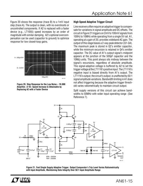
<strong>Application</strong> <strong>Note</strong> <strong>61</strong>Figure 20 shows the response (trace B) to a 1mV inputstep (trace A). The output is clean, with no overshoots oruncontrolled components. If A2 is replaced with a fasterdevice (e.g., LT1055) speed increases by an order ofmagnitude with similar damping. A2’s optional overcompensationcan be used (capacitor to ground) to optimizeresponse <strong>for</strong> low closed-loop gains.A = 500µV/DIVB = 5V/DIV100µs/DIV<strong>AN<strong>61</strong></strong> F20Figure 20. Step Response <strong>for</strong> the Low Noise × 10,000Amplifier. A 10× Speed Increase Is Obtainable byReplacing A2 with a Faster DeviceHigh Speed Adaptive Trigger CircuitLine receivers often require an adaptive trigger to compensate<strong>for</strong> variations in signal amplitude and DC offsets. Thecircuit in Figure 21 triggers on 2mV to 100mV signals from100Hz to 10MHz while operating from a single 5V rail. A1,operating at a gain of 20, provides wideband AC gain. Theoutput of this stage biases a 2-way peak detector (Q1-Q4).The maximum peak is stored in Q2’s emitter capacitor,while the minimum excursion is retained in Q4’s emittercapacitor. The DC value of A1’s output signal’s midpointappears at the junction of the 500pF capacitor and the10MΩ units. This point always sits midway between thesignal’s excursions, regardless of absolute amplitude.This signal-adaptive voltage is buffered by A2 to set thetrigger voltage at the LT1116’s positive input. The LT1116’snegative input is biased directly from A1’s output. TheLT1116’s output, the circuit’s output, is unaffected by 50:1signal amplitude variations. Bandwidth limiting in A1 doesnot affect triggering because the adaptive trigger thresholdvaries ratiometrically to maintain circuit output.Split supply versions of this circuit can achieve bandwidthsto 50MHz with wider input operating range (SeeReference 7).5V3k5VQ1Q25V2k750Ω+A1LT1192–1kQ30.005µF0.005µFQ4500pF3M3M+–5VA2LT1006+10µFINPUT0.01µF+50ΩC1100µFC20.1µFNPN = 2N3904PNP = 2N39063k500Ω1N41481N4148500Ω0.1µF+–5VLT1116QQTRIGGEROUT<strong>AN<strong>61</strong></strong> F21Figure 21. Fast Single Supply Adaptive Trigger. Output Comparator’s Trip Level Varies Ratiometricallywith Input Amplitude, Maintaining Data Integrity Over 50:1 Input Amplitude Range<strong>AN<strong>61</strong></strong>-15