TL494M PULSE-WIDTH-MODULATION CONTROL CIRCUIT
TL494M PULSE-WIDTH-MODULATION CONTROL CIRCUIT
TL494M PULSE-WIDTH-MODULATION CONTROL CIRCUIT
- No tags were found...

Create successful ePaper yourself
Turn your PDF publications into a flip-book with our unique Google optimized e-Paper software.
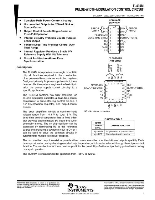
<strong>TL494M</strong><strong>PULSE</strong>-<strong>WIDTH</strong>-<strong>MODULATION</strong> <strong>CONTROL</strong> <strong>CIRCUIT</strong>SGLS041A – D3883, SEPTEMBER 1991 – REVISED MAY 1993• Complete PWM Power Control Circuitry• Uncommitted Outputs for 200-mA Sink orSource Current• Output Control Selects Single-Ended orPush-Pull Operation• Internal Circuitry Prohibits Double Pulse atEither Output• Variable Dead Time Provides Control OverTotal Range• Internal Regulator Provides a Stable 5-VReference Supply With 5% Tolerance• Circuit Architecture Allows EasySynchronizationERROR IN+AMP 1 IN–FEEDBACKDEAD-TIME CTRLC TR TGNDC1J PACKAGE(TOP VIEW)12345678161514131211109FK PACKAGE(TOP VIEW)IN+IN–REFERRORAMP 2OUTPUT CTRLV CCC2E2E1descriptionThe <strong>TL494M</strong> incorporates on a single monolithicchip all functions required in the constructionof a pulse-width-modulation controlled system.Designed primarily for power supply control, thesedevices offer the systems engineer the flexibility totailor the power supply control circuitry to aspecific application.The <strong>TL494M</strong> contains two error amplifiers, anon-chip adjustable oscillator, a dead-time controlcomparator, a pulse-steering control flip-flop, a5-V 5%-precision regulator, and output-controlcircuits.The error amplifiers exhibit a common-modevoltage range from – 0.3 V to V CC –2 V. Thedead-time control comparator has a fixed offsetthat provides approximately 5% dead time whenexternally altered. The on-chip oscillator can bebypassed by terminating R T to the referenceoutput and providing a sawtooth input to C T , or itcan be used to drive the common circuits insynchronous multiple-rail power supplies.FEEDBACKDEAD-TIME CTRLNCC TR TNC – No internal connectionINPUTOUTPUTCTRLVI = GNDVI = REFIN–IN+NCIN+IN–342 1 20 19185671716158149 10 11 12 13GNDC1NCE1E2REFOUTPUT CTRLNCV CCC2The uncommitted output transistors provide either common-emitter or emitter-follower output capability. Eachdevice provides for push-pull or single-ended output operation, which can be selected through the output-controlfunction. The architecture of these devices prohibits the possibility of either output being pulsed twice duringpush-pull operation.The <strong>TL494M</strong> is characterized for operation from –55°C to 125°C.ERRORAMP 1ERRORAMP 2FUNCTION TABLEOUTPUT FUNCTIONSingle-ended or parallel outputNormal push-pull operationPRODUCTION DATA information is current as of publication date.Products conform to specifications per the terms of Texas Instrumentsstandard warranty. Production processing does not necessarily includetesting of all parameters.Copyright © 1993, Texas Instruments IncorporatedOn products compliant to MIL-STD-883, Class B, all parameters aretested unless otherwise noted. On all other products, productionprocessing does not necessarily include testing of all parameters.POST OFFICE BOX 655303 • DALLAS, TEXAS 752651
<strong>TL494M</strong><strong>PULSE</strong>-<strong>WIDTH</strong>-<strong>MODULATION</strong> <strong>CONTROL</strong> <strong>CIRCUIT</strong>SGLS041A – D3883, SEPTEMBER 1991 – REVISED MAY 1993functional block diagramRTCTDEAD-TIMECTRL65≈ 0.1 V4OscillatorDead-Time-ControlComparator1DOUTPUT CTRL(see Function Table)13C1Q189C1E1IN +IN –12Error Amplifier+1–PWMComparatorPulse-SteeringFlip-FlopQ21110C2E2IN +IN –1615Error Amplifier+2–ReferenceRegulator1214VCCREFFEEDBACK30.7 mA7GNDPin numbers shown are for J package.2POST OFFICE BOX 655303 • DALLAS, TEXAS 75265
<strong>TL494M</strong><strong>PULSE</strong>-<strong>WIDTH</strong>-<strong>MODULATION</strong> <strong>CONTROL</strong> <strong>CIRCUIT</strong>SGLS041A – D3883, SEPTEMBER 1991 – REVISED MAY 1993absolute maximum ratings over operating free-air temperature range (unless otherwise noted)NOTES:Supply voltage, V CC (see Note 1) . . . . . . . . . . . . . . . . . . . . . . . . . . . . . . . . . . . . . . . . . . . . . . . . . . . . . . . . . . . 41 VAmplifier input voltage, V I . . . . . . . . . . . . . . . . . . . . . . . . . . . . . . . . . . . . . . . . . . . . . . . . . . . . . . . . . . . . V CC + 0.3 VCollector output voltage . . . . . . . . . . . . . . . . . . . . . . . . . . . . . . . . . . . . . . . . . . . . . . . . . . . . . . . . . . . . . . . . . . . . 41 VCollector output current . . . . . . . . . . . . . . . . . . . . . . . . . . . . . . . . . . . . . . . . . . . . . . . . . . . . . . . . . . . . . . . . . . 250 mAContinuous total dissipation (see Note 2) . . . . . . . . . . . . . . . . . . . . . . . . . . . . . . . . . . . . . . . . . . . . . . . . . 1375 mWOperating free-air temperature range . . . . . . . . . . . . . . . . . . . . . . . . . . . . . . . . . . . . . . . . . . . . . . –55°C to 125°CStorage temperature range . . . . . . . . . . . . . . . . . . . . . . . . . . . . . . . . . . . . . . . . . . . . . . . . . . . . . . . –65°C to 150°CCase temperature for 60 seconds: FK package . . . . . . . . . . . . . . . . . . . . . . . . . . . . . . . . . . . . . . . . . . . . . . 260°CLead temperature 1,6 mm (1/16 inch) from case for 60 seconds: J package . . . . . . . . . . . . . . . . . . . . . 300°C1. All voltage values, except differential voltages, are with respect to the network GND.2. For operation above 25°C free-air temperature, derate linearly to 275 mW at the rate of 11 mW/°C.recommended operating conditionsMIN MAX UNITSupply voltage, VCC 7 40 VAmplifier input voltage, VI –0.3 VCC –2 VCollector output voltage, VO 40 VCollector output current (each transistor) 200 mACurrent into FEEDBACK 0.3 mATiming capacitor, CT 0.47 10000 nFTiming resistor, RT 1.8 500 kΩOscillator frequency, fosc 1 300 kHzOperating free-air temperature, TA –55 125 °CPOST OFFICE BOX 655303 • DALLAS, TEXAS 75265 3
<strong>TL494M</strong><strong>PULSE</strong>-<strong>WIDTH</strong>-<strong>MODULATION</strong> <strong>CONTROL</strong> <strong>CIRCUIT</strong>SGLS041A – D3883, SEPTEMBER 1991 – REVISED MAY 1993electrical characteristics over recommended operating free-air temperature range, V CC = 15 V,f = 10 kHz (unless otherwise noted)reference sectionPARAMETER TEST CONDITIONS MIN TYP† MAX UNITOutput voltage, REF IO = 1 mA 4.75 5 5.25 VInput regulation VCC = 7 V to 40 V 2 25 mVOutput regulation IO = 1 mA to 10 mA 1 15 mVOutput voltage change with temperature ∆TA = MIN to MAX‡ 0.2% 3%*Short-circuit output current§ REF = 0 –25 mAoscillator section, C T = 0.01 µF, R T = 12 kΩ (see Figure 1)PARAMETER TEST CONDITIONS MIN TYP† MAX UNITFrequency 10 kHzStandard deviation of frequency All values of VCC, CT, RT, and TA constant 10%Frequency change with voltage VCC = 7 V to 40 V, TA = 25°C 0.1%Frequency change with temperature# ∆TA = MIN to MAX‡ 1%*error amplifier section (see Figure 2)PARAMETER TEST CONDITIONS MIN TYP† MAX UNITInput offset voltage VO (FEEDBACK) = 2.5 V 2 10 mVInput offset current VO (FEEDBACK) = 2.5 V 25 250 nAInput bias current VO (FEEDBACK) = 2.5 V 0.2 1 µACommon-mode input voltage rangeVCC = 7 V to 40 V0.3toVCC –2Open-loop voltage amplification ∆VO = 3 V, RL = 2 kΩ, VO = 0.5 V to 3.5 V 70 95 dBUnity-gain bandwidth VO = 0.5 V to 3.5 V, RL = 2 kΩ 800 kHzCommon-mode rejection ratio ∆VO = 40 V, TA = 25°C 65 80 dBOutput sink current, FEEDBACK VID = – 15 mV to – 5 V, V (FEEDBACK) = 0.7 V 0.3 0.7 mAOutput source current, FEEDBACK VID = 15 mV to 5 V, V (FEEDBACK) = 3.5 V –2 mA* This parameter is not production tested.† All typical values except for parameter changes with temperature are at TA = 25°C.2‡ For conditions shown as MIN or MAX, use the appropriate value specified under recommended operating conditions. N§ Duration of the short circuit should not exceed one second. (x n X) 2Standard deviation is a measure of the statistical distribution about the mean as derived from the formula:# n 1Temperature coefficient of the timing capacitor and timing resistor is not taken into account.N 1V4POST OFFICE BOX 655303 • DALLAS, TEXAS 75265
<strong>TL494M</strong><strong>PULSE</strong>-<strong>WIDTH</strong>-<strong>MODULATION</strong> <strong>CONTROL</strong> <strong>CIRCUIT</strong>SGLS041A – D3883, SEPTEMBER 1991 – REVISED MAY 1993electrical characteristics over recommended operating free-air temperature range, V CC = 15 V,f = 10 kHz (unless otherwise noted)output sectionPARAMETER TEST CONDITIONS MIN TYP† MAX UNITCollector off-state current VCE = 40 V, VCC = 40 V 2 100 µAEmitter off-state current VCC = VC = 40 V, VE = 0 –100 µACollector-emitter saturation voltageCommon emitter VE = 0, IC = 200 mA 1.1 1.3Emitter follower VC = 15 V, IE = – 200 mA 1.5 2.5Output control input current VI = REF 3.5 mAdead-time control section (see Figure 1)PARAMETER TEST CONDITIONS MIN TYP† MAX UNITInput bias current, DEAD-TIME CTRL VI = 0 to 5.25 V –2 –10 µAMaximum duty cycle, each output VI (DEAD-TIME CTRL) = 0, CT = 0.1 µF, RT = 12 kΩ 45% 50%*Input threshold voltage, DEAD-TIME CTRLpwm comparator section (see Figure 1)Zero duty cycle 3 3.3Maximum duty cycle 0*PARAMETER TEST CONDITIONS MIN TYP† MAX UNITInput threshold voltage, FEEDBACK Zero duty cycle 4 4.5 VInput sink current, FEEDBACK V (FEEDBACK) = 0.7 V 0.3 0.7 mAtotal device (see Figure 1)Standby supply currentPARAMETER TEST CONDITIONS MIN TYP† MAX UNITRT at REF,VCC = 15 V 6 21All other inputs and outputs open VCC = 40 V 9 26Average supply current VI (DEAD-TIME CTRL) = 2 V, See Figure 1 7.5 mAswitching characteristics, T A = 25°COutput voltage rise time, trOutput voltage fall time, tfPARAMETER TEST CONDITIONS MIN TYP† MAX UNITCommon-emitter configuration, See Figure 3Output voltage rise time, trOutput voltage fall time, tfEmitter-follower configuration, See Figure 4* This parameter is not production tested.† All typical values except for temperature coefficient are at TA = 25°C.100 200*25 100*100 200*40 100*VVmAnsnsPOST OFFICE BOX 655303 • DALLAS, TEXAS 75265 5
<strong>TL494M</strong><strong>PULSE</strong>-<strong>WIDTH</strong>-<strong>MODULATION</strong> <strong>CONTROL</strong> <strong>CIRCUIT</strong>SGLS041A – D3883, SEPTEMBER 1991 – REVISED MAY 1993PARAMETER MEASUREMENT INFORMATIONVCC = 15 VTestInputs4312 kΩ650.01 µF121615VCCDEAD-TIMECTRLFEEDBACKRTCTIN +IN –IN +IN –12ErrorAmplifiers150 Ω,2 W150 Ω,2 WC18Output 1E19C211Output 2E21050 kΩ13OUTPUTCTRLGND7REF14TEST <strong>CIRCUIT</strong>Voltageat C1Voltageat C2VCC0 VVCC0 VVoltageat CTDEAD-TIME<strong>CONTROL</strong>Threshold Voltage0 VThreshold VoltageFEEDBACK0.7 VDuty Cycle0%MAX0%VOLTAGE WAVEFORMSFigure 1. Operational Test Circuit and Waveforms6POST OFFICE BOX 655303 • DALLAS, TEXAS 75265
<strong>TL494M</strong><strong>PULSE</strong>-<strong>WIDTH</strong>-<strong>MODULATION</strong> <strong>CONTROL</strong> <strong>CIRCUIT</strong>PARAMETER MEASUREMENT INFORMATIONSGLS041A – D3883, SEPTEMBER 1991 – REVISED MAY 1993Amplifier Under Test+VI–FEEDBACK+REF–Other AmplifierFigure 2. Amplifier Characteristics15 VEach OutputCircuit68 Ω,2 WOutput90%tftr90%CL = 15 pF(includes probe andjig capacitance)10%10%TEST <strong>CIRCUIT</strong>OUTPUT VOLTAGE WAVEFORMFigure 3. Common-Emitter Configuration15 VEach OutputCircuit90%90%Output10%10%CL = 15 pF(includes probe andjig capacitance)68 Ω,2 WtrOUTPUT VOLTAGE WAVEFORMtfTEST <strong>CIRCUIT</strong>Figure 4. Emitter-Follower ConfigurationPOST OFFICE BOX 655303 • DALLAS, TEXAS 75265 7
<strong>TL494M</strong><strong>PULSE</strong>-<strong>WIDTH</strong>-<strong>MODULATION</strong> <strong>CONTROL</strong> <strong>CIRCUIT</strong>SGLS041A – D3883, SEPTEMBER 1991 – REVISED MAY 1993TYPICAL CHARACTERISTICSOscillator Frequency – Hz100 k40 k10 k4 k1 k40010040OSCILLATOR FREQUENCY ANDFREQUENCY VARIATION †vsTIMING RESISTANCE–2%–1%CT = 1 µF0%0.1 µF0.01 µFVCC = 15 VTA = 25°C0.001 µF∆f† = 1%101 k 4 k 10 k 40 k 100 k 400 k 1 MRT – Timing Resistance – Ω† Frequency variation (∆f) is the change in oscillator frequency that occurs over the full temperature range.Figure 51009080AMPLIFIER VOLTAGE AMPLIFICATIONvsFREQUENCYVCC = 15 V∆VO = 3 VTA = 25°CVoltage Amplification – dB7060504030201001 10 100 1 k 10 k 100 k 1 Mf – Frequency – HzFigure 6Printed 8 in U.S.A.POST OFFICE BOX 655303 • DALLAS, TEXAS 75265SGLS041A
IMPORTANT NOTICETexas Instruments (TI) reserves the right to make changes to its products or to discontinue any semiconductorproduct or service without notice, and advises its customers to obtain the latest version of relevant informationto verify, before placing orders, that the information being relied on is current.TI warrants performance of its semiconductor products and related software to the specifications applicable atthe time of sale in accordance with TI’s standard warranty. Testing and other quality control techniques areutilized to the extent TI deems necessary to support this warranty. Specific testing of all parameters of eachdevice is not necessarily performed, except those mandated by government requirements.Certain applications using semiconductor products may involve potential risks of death, personal injury, orsevere property or environmental damage (“Critical Applications”).TI SEMICONDUCTOR PRODUCTS ARE NOT DESIGNED, INTENDED, AUTHORIZED, OR WARRANTEDTO BE SUITABLE FOR USE IN LIFE-SUPPORT APPLICATIONS, DEVICES OR SYSTEMS OR OTHERCRITICAL APPLICATIONS.Inclusion of TI products in such applications is understood to be fully at the risk of the customer. Use of TIproducts in such applications requires the written approval of an appropriate TI officer. Questions concerningpotential risk applications should be directed to TI through a local SC sales office.In order to minimize risks associated with the customer’s applications, adequate design and operatingsafeguards should be provided by the customer to minimize inherent or procedural hazards.TI assumes no liability for applications assistance, customer product design, software performance, orinfringement of patents or services described herein. Nor does TI warrant or represent that any license, eitherexpress or implied, is granted under any patent right, copyright, mask work right, or other intellectual propertyright of TI covering or relating to any combination, machine, or process in which such semiconductor productsor services might be or are used.Copyright © 1995, Texas Instruments Incorporated