74AHC573; 74AHCT573 Octal D-type transparant latch; 3-state
74AHC573; 74AHCT573 Octal D-type transparant latch; 3-state
74AHC573; 74AHCT573 Octal D-type transparant latch; 3-state

You also want an ePaper? Increase the reach of your titles
YUMPU automatically turns print PDFs into web optimized ePapers that Google loves.
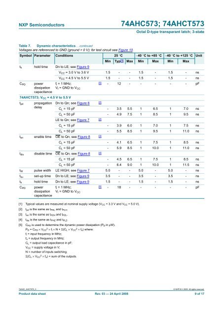
NXP Semiconductors<strong>74AHC573</strong>; <strong>74AHCT573</strong><strong>Octal</strong> D-<strong>type</strong> <strong>transparant</strong> <strong>latch</strong>; 3-<strong>state</strong>Table 7. Dynamic characteristics …continuedVoltages are referenced to GND (ground = 0 V); for test circuit see Figure 10.Symbol Parameter Conditions 25 °C −40 °C to +85 °C −40 °C to +125 °C Unitt h hold time Dn to LE; see Figure 9V CC = 3.0 V to 3.6 V 1.5 - - 1.5 - 1.5 - nsV CC = 4.5 V to 5.5 V 1.5 - - 1.5 - 1.5 - nsC PDpowerdissipationcapacitancef i = 1 MHz;[5]- 12 - - - - - pFV I = GND to V CC<strong>74AHCT573</strong>; V CC = 4.5 V to 5.5 Vt pd propagation Dn to Qn; see Figure 6[2]delayC L = 15 pF - 3.5 5.5 1 6.5 1 7.0 nsC L = 50 pF - 4.9 7.5 1 8.5 1 9.5 nsLE to Qn; see Figure 7[2]C L = 15 pF - 3.9 6.0 1 7.0 1 7.5 nsC L = 50 pF - 5.5 8.5 1 9.5 1 11.0 nst en enable time OE to Qn; see Figure 8[3]C L = 15 pF - 4.1 6.5 1 7.5 1 8.5 nsC L = 50 pF - 5.9 8.5 1 10.0 1 11.0 nst dis disable time OE to Qn; see Figure 8[4]C L = 15 pF - 4.5 6.5 1 7.5 1 8.5 nsC L = 50 pF - 6.4 9.0 1 10.0 1 11.5 nst W pulse width LE HIGH; see Figure 7 5.0 - - 5.0 - 5.0 - nst su set-up time Dn to LE; see Figure 9 3.5 - - 3.5 - 3.5 - nst h hold time Dn to LE; see Figure 9 1.5 - - 1.5 - 1.5 - nsC PDpowerdissipationcapacitancef i = 1 MHz;[5]- 18 - - - - - pFV I = GND to V CC[1] Typical values are measured at nominal supply voltage (V CC = 3.3 V and V CC = 5.0 V).[2] t pd is the same as t PHL and t PLH .[3] t en is the same as t PZH and t PZL .[4] t dis is the same as t PHZ and t PLZ .[5] C PD is used to determine the dynamic power dissipation (P D in µW).P D =C PD × V 2 CC × f i × N+Σ(C L × V 2 CC × f o ) where:f i = input frequency in MHz;f o = output frequency in MHz;C L = output load capacitance in pF;V CC = supply voltage in V;N = number of inputs switching;Σ(C L × V 2 CC × f o ) = sum of the outputs.Min Typ [1] Max Min Max Min Max74AHC_AHCT573_3© NXP B.V. 2008. All rights reserved.Product data sheet Rev. 03 — 24 April 2008 9 of 17