
Create successful ePaper yourself
Turn your PDF publications into a flip-book with our unique Google optimized e-Paper software.
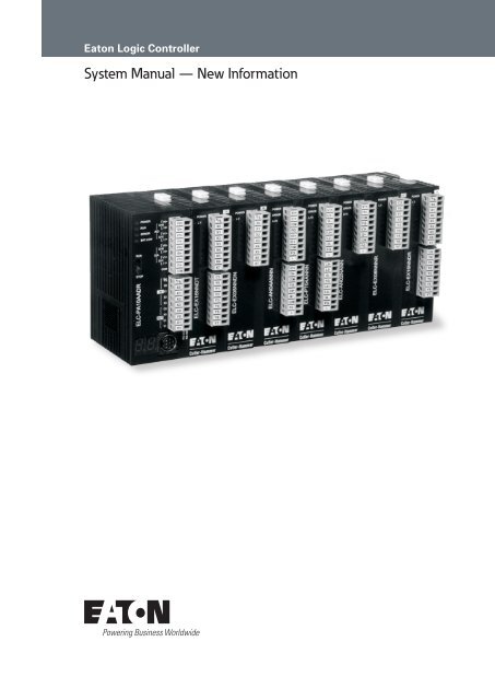
Eaton Logic Controller<strong>System</strong> <strong>Manual</strong> — New Information
Eaton Logic ControllerNovember 2008Disclaimer of Warranties and Limitation of LiabilityThe information, recommendations, descriptions and safety notations in this document arebased on Eaton Electrical Inc. and/or Eaton Corporation’s (“Eaton”) experience and judgmentand may not cover all contingencies. If further information is required, an Eaton sales officeshould be consulted.Sale of the product shown in this literature is subject to the terms and conditions outlinedin appropriate Eaton selling policies or other contractual agreement between Eaton andthe purchaser.THERE ARE NO UNDERSTANDINGS, AGREEMENTS, WARRANTIES, EXPRESSED ORIMPLIED, INCLUDING WARRANTIES OF FITNESS FOR A PARTICULAR PURPOSE ORMERCHANTABILITY, OTHER THAN THOSE SPECIFICALLY SET OUT IN ANY EXISTINGCONTRACT BETWEEN THE PARTIES. ANY SUCH CONTRACT STATES THE ENTIREOBLIGATION OF EATON. THE CONTENTS OF THIS DOCUMENT SHALL NOT BECOME PARTOF OR MODIFY ANY CONTRACT BETWEEN THE PARTIES. In no event will Eaton beresponsible to the purchaser or user in contract, in tort (including negligence), strict liabilityor otherwise for any special, indirect, incidental or consequential damage or loss whatsoever,including but not limited to damage or loss of use of equipment, plant or power system, costof capital, loss of power, additional expenses in the use of existing power facilities, or claimsagainst the purchaser or user by its customers resulting from the use of the information,recommendations and descriptions contained herein.The information contained in this manual is subject to change without notice.PRELIMINARY DRAFTMN05003003E For more information visit: www.eaton.com i
Eaton Logic ControllerNovember 2008Table of ContentsPREFACE . . . . . . . . . . . . . . . . . . . . . . . . . . . . . . . . . . . . . . . . . . . . . . . . . . . . . . . . . . . . . . . . . ICHAPTER 1 — PRODUCT OVERVIEW. . . . . . . . . . . . . . . . . . . . . . . . . . . . . . . . . . . . . . . . . . 1-11.1 - <strong>ELC</strong> Processors. . . . . . . . . . . . . . . . . . . . . . . . . . . . . . . . . . . . . . . . . . . . . . . . . . . . 1-21.2 - <strong>ELC</strong> Digital Modules. . . . . . . . . . . . . . . . . . . . . . . . . . . . . . . . . . . . . . . . . . . . . . . . 1-41.3 - <strong>ELC</strong> Specialty Modules . . . . . . . . . . . . . . . . . . . . . . . . . . . . . . . . . . . . . . . . . . . . . 1-51.4 - <strong>ELC</strong> Power Supplies. . . . . . . . . . . . . . . . . . . . . . . . . . . . . . . . . . . . . . . . . . . . . . . . 1-71.5 - <strong>ELC</strong>Soft Programming Software . . . . . . . . . . . . . . . . . . . . . . . . . . . . . . . . . . . . . 1-81.6 - <strong>ELC</strong>-HHP . . . . . . . . . . . . . . . . . . . . . . . . . . . . . . . . . . . . . . . . . . . . . . . . . . . . . . . . . 1-91.7 - <strong>ELC</strong> Graphic Panels . . . . . . . . . . . . . . . . . . . . . . . . . . . . . . . . . . . . . . . . . . . . . . . . 1-91.8 - <strong>ELC</strong>SoftGP Programming Software . . . . . . . . . . . . . . . . . . . . . . . . . . . . . . . . . . . 1-11CHAPTER 2 — GETTING STARTED . . . . . . . . . . . . . . . . . . . . . . . . . . . . . . . . . . . . . . . . . . . . 2-12.1 - Connect <strong>ELC</strong> Power . . . . . . . . . . . . . . . . . . . . . . . . . . . . . . . . . . . . . . . . . . . . . . . . 2-22.2 - Connect <strong>ELC</strong> to a PC . . . . . . . . . . . . . . . . . . . . . . . . . . . . . . . . . . . . . . . . . . . . . . . 2-22.3 - Connect <strong>ELC</strong> to the <strong>ELC</strong>-HHP . . . . . . . . . . . . . . . . . . . . . . . . . . . . . . . . . . . . . . . . 2-42.4 - Current Consumed by the Control Unit . . . . . . . . . . . . . . . . . . . . . . . . . . . . . . . . 2-52.5 - I/O Allocation . . . . . . . . . . . . . . . . . . . . . . . . . . . . . . . . . . . . . . . . . . . . . . . . . . . . . 2-72.6 - Install <strong>ELC</strong>Soft . . . . . . . . . . . . . . . . . . . . . . . . . . . . . . . . . . . . . . . . . . . . . . . . . . . . 2-92.7 - Enter this Program . . . . . . . . . . . . . . . . . . . . . . . . . . . . . . . . . . . . . . . . . . . . . . . . . 2-102.8 - Download the Program . . . . . . . . . . . . . . . . . . . . . . . . . . . . . . . . . . . . . . . . . . . . . 2-102.9 - Monitor the Program . . . . . . . . . . . . . . . . . . . . . . . . . . . . . . . . . . . . . . . . . . . . . . . 2-10CHAPTER 3 — INSTALLATION. . . . . . . . . . . . . . . . . . . . . . . . . . . . . . . . . . . . . . . . . . . . . . . . 3-13.1 - <strong>ELC</strong> Mounting and Clearance . . . . . . . . . . . . . . . . . . . . . . . . . . . . . . . . . . . . . . . . 3-23.2 - Installing Modules . . . . . . . . . . . . . . . . . . . . . . . . . . . . . . . . . . . . . . . . . . . . . . . . . 3-33.3 - DIN Rail Installation . . . . . . . . . . . . . . . . . . . . . . . . . . . . . . . . . . . . . . . . . . . . . . . . 3-43.4 - Wiring . . . . . . . . . . . . . . . . . . . . . . . . . . . . . . . . . . . . . . . . . . . . . . . . . . . . . . . . . . . 3-53.5 - Dimensions. . . . . . . . . . . . . . . . . . . . . . . . . . . . . . . . . . . . . . . . . . . . . . . . . . . . . . . 3-153.6 - Terminal Layouts . . . . . . . . . . . . . . . . . . . . . . . . . . . . . . . . . . . . . . . . . . . . . . . . . . 3-20CHAPTER 4 — <strong>ELC</strong> CONCEPTS . . . . . . . . . . . . . . . . . . . . . . . . . . . . . . . . . . . . . . . . . . . . . . . 4.14.1 - <strong>ELC</strong> Scan Method. . . . . . . . . . . . . . . . . . . . . . . . . . . . . . . . . . . . . . . . . . . . . . . . . . 4-24.2 - Current Flow . . . . . . . . . . . . . . . . . . . . . . . . . . . . . . . . . . . . . . . . . . . . . . . . . . . . . . 4-34.3 - Contact A, Contact B . . . . . . . . . . . . . . . . . . . . . . . . . . . . . . . . . . . . . . . . . . . . . . . 4-44.4 - <strong>ELC</strong> Registers and Relays . . . . . . . . . . . . . . . . . . . . . . . . . . . . . . . . . . . . . . . . . . . 4-44.5 - Ladder Logic Symbols . . . . . . . . . . . . . . . . . . . . . . . . . . . . . . . . . . . . . . . . . . . . . . 4-54.6 - Conversion of <strong>ELC</strong> Commands and Each Diagram Structure . . . . . . . . . . . . . . 4-114.7 - <strong>ELC</strong>-HHP Programming Methods . . . . . . . . . . . . . . . . . . . . . . . . . . . . . . . . . . . . . 4-124.8 - Simplifying Ladder Logic . . . . . . . . . . . . . . . . . . . . . . . . . . . . . . . . . . . . . . . . . . . 4-144.9 - Basic Ladder Logic Examples . . . . . . . . . . . . . . . . . . . . . . . . . . . . . . . . . . . . . . . . 4-17PRELIMINARY DRAFTii For more information visit: www.eaton.com MN05003003E
Eaton Logic ControllerNovember 2008Table of Contents (Continued)CHAPTER 5 — PROGRAMMING CONCEPTS . . . . . . . . . . . . . . . . . . . . . . . . . . . . . . . . . . . . 5-15.1 - <strong>ELC</strong> Memory Map for PB Model. . . . . . . . . . . . . . . . . . . . . . . . . . . . . . . . . . . . . . 5-25.2 - <strong>ELC</strong> Memory Map for PC/PA/PH Models . . . . . . . . . . . . . . . . . . . . . . . . . . . . . . . 5-45.3 - <strong>ELC</strong> Memory Map for PV Models. . . . . . . . . . . . . . . . . . . . . . . . . . . . . . . . . . . . . 5-75.4 - <strong>ELC</strong> Latched Memory Settings . . . . . . . . . . . . . . . . . . . . . . . . . . . . . . . . . . . . . . . 5-105.5 - <strong>ELC</strong> Latched Memory Modes . . . . . . . . . . . . . . . . . . . . . . . . . . . . . . . . . . . . . . . . 5-125.6 - <strong>ELC</strong> Bits, Nibbles, Bytes, Words, etc . . . . . . . . . . . . . . . . . . . . . . . . . . . . . . . . . . 5-135.7 - Binary, Octal, Decimal, BCD, Hex . . . . . . . . . . . . . . . . . . . . . . . . . . . . . . . . . . . . . 5-135.8 - M Relay. . . . . . . . . . . . . . . . . . . . . . . . . . . . . . . . . . . . . . . . . . . . . . . . . . . . . . . . . . 5-155.9 - S Relay . . . . . . . . . . . . . . . . . . . . . . . . . . . . . . . . . . . . . . . . . . . . . . . . . . . . . . . . . . 5-345.10 - T (Timer) . . . . . . . . . . . . . . . . . . . . . . . . . . . . . . . . . . . . . . . . . . . . . . . . . . . . . . . . 5-345.11 - C (Counter) . . . . . . . . . . . . . . . . . . . . . . . . . . . . . . . . . . . . . . . . . . . . . . . . . . . . . . 5-355.12 - High-speed Counters. . . . . . . . . . . . . . . . . . . . . . . . . . . . . . . . . . . . . . . . . . . . . . 5-375.13 - D (Word register) . . . . . . . . . . . . . . . . . . . . . . . . . . . . . . . . . . . . . . . . . . . . . . . . . 5-505.14 - E, F Index . . . . . . . . . . . . . . . . . . . . . . . . . . . . . . . . . . . . . . . . . . . . . . . . . . . . . . . 5-655.15 - File Register . . . . . . . . . . . . . . . . . . . . . . . . . . . . . . . . . . . . . . . . . . . . . . . . . . . . . 5-655.16 - Nest Level Pointer[N], Pointer[P] and Interrupt Pointer [I]. . . . . . . . . . . . . . . . 5-665.17 - Special M Relay and Special D Register Application . . . . . . . . . . . . . . . . . . . . 5-705.18 - Fault Code Information . . . . . . . . . . . . . . . . . . . . . . . . . . . . . . . . . . . . . . . . . . . . 5-124CHAPTER 6 — INSTRUCTION SET . . . . . . . . . . . . . . . . . . . . . . . . . . . . . . . . . . . . . . . . . . . . 6-16.1 - Basic Instruction Explanations . . . . . . . . . . . . . . . . . . . . . . . . . . . . . . . . . . . . . . . 6-26.2 - Pointers . . . . . . . . . . . . . . . . . . . . . . . . . . . . . . . . . . . . . . . . . . . . . . . . . . . . . . . . . 6-106.3 - Interrupt Pointers. . . . . . . . . . . . . . . . . . . . . . . . . . . . . . . . . . . . . . . . . . . . . . . . . . 6-116.4 - Basic Instructions (without API numbers) . . . . . . . . . . . . . . . . . . . . . . . . . . . . . . 6-136.5 - Application Programming Instructions . . . . . . . . . . . . . . . . . . . . . . . . . . . . . . . . 6-146.6 - Numerical List of Instructions. . . . . . . . . . . . . . . . . . . . . . . . . . . . . . . . . . . . . . . . 6-256.7 - Detailed Instruction Explanation . . . . . . . . . . . . . . . . . . . . . . . . . . . . . . . . . . . . . 6-34CHAPTER 7 — COMMUNICATIONS . . . . . . . . . . . . . . . . . . . . . . . . . . . . . . . . . . . . . . . . . . . 7-17.1 - Communication Ports . . . . . . . . . . . . . . . . . . . . . . . . . . . . . . . . . . . . . . . . . . . . . . 7.27.2 - Communication Protocol ASCII Mode. . . . . . . . . . . . . . . . . . . . . . . . . . . . . . . . . 7.37.3 - Communication Protocol RTU Mode . . . . . . . . . . . . . . . . . . . . . . . . . . . . . . . . . . 7-87.4 - <strong>ELC</strong> Device Address . . . . . . . . . . . . . . . . . . . . . . . . . . . . . . . . . . . . . . . . . . . . . . . 7-127.5 - Command Code. . . . . . . . . . . . . . . . . . . . . . . . . . . . . . . . . . . . . . . . . . . . . . . . . . . 7-147.6 - <strong>ELC</strong> Device Addresses by Controller . . . . . . . . . . . . . . . . . . . . . . . . . . . . . . . . . . 7-22CHAPTER 8 — SFC PROGRAMMING . . . . . . . . . . . . . . . . . . . . . . . . . . . . . . . . . . . . . . . . . . 8-18.1 - Step Ladder Command [STL], [RET] . . . . . . . . . . . . . . . . . . . . . . . . . . . . . . . . . . 8-28.2 - Sequential Function Chart (SFC) . . . . . . . . . . . . . . . . . . . . . . . . . . . . . . . . . . . . . 8-38.3 - Step Ladder Command Explanation . . . . . . . . . . . . . . . . . . . . . . . . . . . . . . . . . . 8-58.4 - Reminder of Design on the Step Ladder Program . . . . . . . . . . . . . . . . . . . . . . . 8-118.5 - Categories of Procedures . . . . . . . . . . . . . . . . . . . . . . . . . . . . . . . . . . . . . . . . . . . 8-138.6 - IST Command . . . . . . . . . . . . . . . . . . . . . . . . . . . . . . . . . . . . . . . . . . . . . . . . . . . . 8-24CHAPTER 9 — TROUBLESHOOTING . . . . . . . . . . . . . . . . . . . . . . . . . . . . . . . . . . . . . . . . . . . . 9-19.1 - Common Problems and Solution. . . . . . . . . . . . . . . . . . . . . . . . . . . . . . . . . . . . . . . 9-29.2 - Fault Code Table . . . . . . . . . . . . . . . . . . . . . . . . . . . . . . . . . . . . . . . . . . . . . . . . . . . . 9-49.3 - Error Detection Devices . . . . . . . . . . . . . . . . . . . . . . . . . . . . . . . . . . . . . . . . . . . . . . 9-79.4 - Periodic Inspection . . . . . . . . . . . . . . . . . . . . . . . . . . . . . . . . . . . . . . . . . . . . . . . . . . 9-7PRELIMINARY DRAFTMN05003003E For more information visit: www.eaton.com iii
Eaton Logic ControllerNovember 2008Table of Contents (Continued)CHAPTER 10 — HANDHELD PROGRAMMER . . . . . . . . . . . . . . . . . . . . . . . . . . . . . . . . . . . . 10.110.1 - Introduction . . . . . . . . . . . . . . . . . . . . . . . . . . . . . . . . . . . . . . . . . . . . . . . . . . . . . 10-210.2 - <strong>ELC</strong>-HHP Standard Specification . . . . . . . . . . . . . . . . . . . . . . . . . . . . . . . . . . . . 10-410.3 - Initial Setup. . . . . . . . . . . . . . . . . . . . . . . . . . . . . . . . . . . . . . . . . . . . . . . . . . . . . . 10-610.4 - <strong>ELC</strong>-HHP Program Read/Write . . . . . . . . . . . . . . . . . . . . . . . . . . . . . . . . . . . . . . 10-1410.5 - Program Mode . . . . . . . . . . . . . . . . . . . . . . . . . . . . . . . . . . . . . . . . . . . . . . . . . . . 10-2610.6 - <strong>ELC</strong> RUN/STOP Mode . . . . . . . . . . . . . . . . . . . . . . . . . . . . . . . . . . . . . . . . . . . . . 10-3610.7 - MON/TEST Mode . . . . . . . . . . . . . . . . . . . . . . . . . . . . . . . . . . . . . . . . . . . . . . . . . 10-3710.8 - Clear User’s Program Memory . . . . . . . . . . . . . . . . . . . . . . . . . . . . . . . . . . . . . . 10-4310.9 - <strong>ELC</strong> and <strong>ELC</strong>-HHP Program Verifications . . . . . . . . . . . . . . . . . . . . . . . . . . . . . . 10-4510.10 - Parameters Settings. . . . . . . . . . . . . . . . . . . . . . . . . . . . . . . . . . . . . . . . . . . . . . 10-4710.11 - M_CARD Functions . . . . . . . . . . . . . . . . . . . . . . . . . . . . . . . . . . . . . . . . . . . . . . 10-5010.12 - File Register . . . . . . . . . . . . . . . . . . . . . . . . . . . . . . . . . . . . . . . . . . . . . . . . . . . . 10-5110.13 - Error Code Explanations . . . . . . . . . . . . . . . . . . . . . . . . . . . . . . . . . . . . . . . . . . 10-5410.14 - Instruction Table. . . . . . . . . . . . . . . . . . . . . . . . . . . . . . . . . . . . . . . . . . . . . . . . . 10-5710.15 - Troubleshooting and Error Message . . . . . . . . . . . . . . . . . . . . . . . . . . . . . . . . 10-6410.16 - <strong>ELC</strong>-HHP Connection . . . . . . . . . . . . . . . . . . . . . . . . . . . . . . . . . . . . . . . . . . . . . 10-6510.17 - <strong>ELC</strong>-HHP Operation Flow Chart . . . . . . . . . . . . . . . . . . . . . . . . . . . . . . . . . . . . 10-66PRELIMINARY DRAFTiv For more information visit: www.eaton.com MN05003003E
Eaton Logic ControllerNovember 2008SafetyDefinitions and SymbolsHazardous High VoltageWARNINGThis symbol indicates high voltage. It calls your attention to itemsor operations that could be dangerous to you and other personsoperating this equipment. Read the message and follow theinstructions carefully.This symbol is the “Safety Alert Symbol.” It occurs with either oftwo signal words: CAUTION or WARNING, as described below.WARNINGIndicates a potentially hazardous situation which, if not avoided,can result in serious injury or death.CAUTIONIndicates a potentially hazardous situation which, if not avoided,can result in minor to moderate injury, or serious damage to theproduct. The situation described in the CAUTION may, if notavoided, lead to serious results. Important safety measures aredescribed in CAUTION (as well as WARNING).WARNINGMotor control equipment and electronic controllers are connectedto hazardous line voltages. When servicing drives and electroniccontrollers, there may be exposed components with housings orprotrusions at or above line potential. Extreme care should be takento protect against shock.• Stand on an insulating pad and make it a habit to use only onehand when checking components.• Always work with another person in case an emergency occurs.Disconnect power before checking controllers or performingmaintenance.• Be sure equipment is properly grounded.PRELIMINARY DRAFT• Wear safety glasses whenever working on electronic controllersor rotating machinery.MN05003003E For more information visit: www.eaton.com v
Eaton Logic ControllerNovember 2008Warnings and CautionsCAUTIONExplosion hazard. Substitution of components may impairsuitability for Class I, Division 2.WARNINGExplosion hazard. Do not replace components unless power hasbeen switched off or area is known to be non-hazardous.PRELIMINARY DRAFTvi For more information visit: www.eaton.com MN05003003E
Product OverviewThe Eaton Logic Controller (<strong>ELC</strong>) is programmable logic controller spanning an I/O of10 – 512 I/O points. <strong>ELC</strong> processors are so versatile they range from nano to small -PLCs I/O and application size without ever needing to change processors. <strong>ELC</strong> cancontrol a wide variety of devices to solve your automation needs. Like most PLCs, <strong>ELC</strong>monitors inputs and modifies outputs as controlled by the user program. User programprovides features like Boolean logic, counting, timing, complex math operations, andcommunications to other communicating products.This Chapter Contains1.1 <strong>ELC</strong> Processors........................................................................................................................ 1-21.2 <strong>ELC</strong> Digital Modules................................................................................................................. 1-41.3 <strong>ELC</strong> Specialty Modules ............................................................................................................ 1-51.4 <strong>ELC</strong> Power Supplies................................................................................................................. 1-71.5 <strong>ELC</strong>Soft Programming Software............................................................................................. 1-81.6 <strong>ELC</strong>-HHP.................................................................................................................................... 1-91.7 <strong>ELC</strong> Graphic Panels ................................................................................................................. 1-91.8 <strong>ELC</strong>SoftGP Programming Software...................................................................................... 1-111-1
<strong>ELC</strong> <strong>System</strong> <strong>Manual</strong>1 Product Overview1.1 <strong>ELC</strong> ProcessorsThe decision is easy when selecting an <strong>ELC</strong> processor. All <strong>ELC</strong> have the same internal features suchas I/O capability; register size, latched memory, communications, etc. The only choice needed is tochoose whether the processor should have included analog in and out or all digital I/O.<strong>ELC</strong>-PB14xxxx <strong>ELC</strong>-PC12xxxx <strong>ELC</strong>-PA10xxxx <strong>ELC</strong>-PH12xxxx <strong>ELC</strong>-PV28xxxxItems <strong>ELC</strong>-PB14xxxx <strong>ELC</strong>-PC12xxxx <strong>ELC</strong>-PA10xxxx <strong>ELC</strong>-PH12xxxx <strong>ELC</strong>-PV28xxxxDimensionsW x H x D(mm)MaximumI/OI/O pointsI/O TypeExecutionSpeedProgramlanguageProgramCapacityDataMemoryCapacity(bits)DataMemoryCapacity(words)IndexRegisters1.00 x 3.54 x2.36(25.2 x 90 x 60)Total:14 pointsDigital Input: 8Digital Output: 61.47 x 3.54 x 2.36 (37.4 x 90 x 60)256 (128 In / 128 Out) Any number of modulesTotal: 12 pointsDigital Input: 8Digital Output: 4Total: 10 pointsDigital input: 4Digital output: 2Analog input: 2Analog output: 2Basic commands – 2µ seconds minimumCommands + Ladder Logic + SFCTotal: 12 pointsDigital Input: 8Digital output: 4(Transistor)2.75 x 3.54 x2.36(70 x 90 x 60)512 (256 In / 256Out)Total: 28 pointsDigital Input: 16Digital output: 12Basiccommands –0.24µ secondsminimum3792 Steps 7920 Steps 15872 Steps1280 Bits 4096 Bits 4096 Bits744 Words 5000 Words 10000 Words2 Words 8 Words 16 Words1-2
1. Product OverviewItems <strong>ELC</strong>-PB14xxxx <strong>ELC</strong>-PC12xxxx <strong>ELC</strong>-PA10xxxx <strong>ELC</strong>-PH12xxxx <strong>ELC</strong>-PV28xxxxFileMemoryCapacityCommandsFloatingPointSFCCommandsTimersCountersHigh SpeedcountersPulseOutputMasterControlLoop- 1600 Words 10000 Words32 Basic / 109Advanced32 Basic / 177 AdvancedYes128 Steps 1024 Steps128 (1ms –100ms)128 (16/32 bit)(Up/Down)131ph-1 input * 41ph-2 input * 12ph-2input * 12 channels,10KHz Max161ph-1 input * 61ph-2 input * 12ph-2 input * 12 channels, 50KHz Max256 (1ms – 100ms)235 (16/32 bit) (Up/Down)8 Loops 8 LoopsSubroutines 64 Subroutines 256 SubroutinesInterruptsReal-timeClock /CalendarSpecialtyExpansionsmodulesSerial PortsSpecialFeatures6(External / Timer/ Comm.)191ph-1 input * 81ph-2 input * 22ph-2 input * 24 channels,100KHz Max15 (External / Timer / HS CNTR / Comm.)- Built-in-8 (Analog In / Analog Out / PT / TC) Modules do not count in total I/O2Potentiometers2 (RS-232 / RS-485)27-SEG displays2Potentiometers32 Basic / 195Advanced181ph-1 input * 101ph-2 input * 42ph-2 input * 44 channels,200KHz Max22 (External /Timer / HS CNTR/ Comm.)2Potentiometers1-3
<strong>ELC</strong> <strong>System</strong> <strong>Manual</strong>1.2 <strong>ELC</strong> Digital Modules<strong>ELC</strong> expansion modules provide the correct amount of I/O for application solutions. Choose 4 , 6 , 8 ,or 16 I/O. Any number of expansion modules can be added to the <strong>ELC</strong> processor to create 256 I/O.ModelDimensionsW x H x D (mm)PowerInput UnitOutput UnitPoint Type Point Type0.99 x 3.54 x 2.36 (25.2 x 90 x 60)<strong>ELC</strong>-EX08NNAN 8 AC 0 None<strong>ELC</strong>-EX08NNDN 8 0 None<strong>ELC</strong>-EX08NNSN 1 8 0 None<strong>ELC</strong>-EX08NNNR 0 8 Relay<strong>ELC</strong>-EX08NNNT 0DC Sink8 Transistor<strong>ELC</strong>-EX06NNNI 0 or6 RelaySource<strong>ELC</strong>-EX08NNDR 4 4Relay<strong>ELC</strong>-EX16NNDR 8 824VDC 2 8<strong>ELC</strong>-EX08NNDT 4 4<strong>ELC</strong>-EX16NNDT8TransistorNote 1: Digital Inputs Simulator module.Note 2: Supplied by bus power from Processor unit.1-4
1. Product Overview1.3 <strong>ELC</strong> Specialty Modules1.3.1 Expansion ModulesIn addition the to expansion I/O, specialty modules like Analog In, Analog Out, Platinum Temperature,Thermocouple, etc.ModelDimensionsW x H x D (mm)PowerInput UnitOutput UnitPoint Type Point Type0.99 x 3.54 x 2.36 (25.2 x 90 x 60)<strong>ELC</strong>-AN02NANN 0 2<strong>ELC</strong>-AN04NANN 0-20mA~20mA4<strong>ELC</strong>-AN06AANN 4-10V ~ +10 V24VDC2<strong>ELC</strong>-AN04ANNN 400~20mA0V ~ +10 V<strong>ELC</strong>-PT04ANNN 4 Platinum Temp. 0-<strong>ELC</strong>-TC04ANNN4 Thermocouple 0Model Power FunctionDimensionsW x H x D (mm)<strong>ELC</strong>-MC01 24VDC Motion Control Unit0.99 x 3.54 x 2.36 (25.2 x 90 x 60)<strong>ELC</strong>-CODNET<strong>ELC</strong>-COPBDP<strong>ELC</strong>-485APTR-DeviceNet Slave UnitProfibus Slave UnitRS-485 Adapter1-5
32324141505069697878<strong>ELC</strong> <strong>System</strong> <strong>Manual</strong>1.3.2 Fast Expansion ModulesThe below modules are only available for the PV Controller and are connected to the left side of the PV.Specific fast expansion bus:MSNS1x100x10DR 1DR 0IN 1IN 0Model Power Function<strong>ELC</strong>-CODENETM<strong>ELC</strong>-COENETM-DeviceNet Network ScannerEthernet Communication Module1-6
1. Product Overview1.4 <strong>ELC</strong> Power SuppliesAll <strong>ELC</strong> modules operate from 24 VDC. These power supplies provide a convenient way to providerobust DC voltage.ItemDimensionsW x H x D (mm)Input PowerOutput VoltsModel<strong>ELC</strong>-PS01<strong>ELC</strong>-PS021.44 x 3.54 x 2.36 (36.5 x 90 x 60) 2.17 x 3.54 x 2.36 (55 x 90 x 60)100~240VAC 50/60Hz24VDCOutput Current (A) 1 A 2 A1-7
<strong>ELC</strong> <strong>System</strong> <strong>Manual</strong>1.5 <strong>ELC</strong>Soft Programming Software<strong>ELC</strong>Soft programming software configures all <strong>ELC</strong> controllers. With <strong>ELC</strong>Soft, applications can becreated, edited, monitored, forced, etc. Move programs from one controller to a different one with ease.Requirements:• Operating <strong>System</strong>s – Windows 98, Windows ME, Windows 2000, Windows XP.• Hard Drive – At least 100M bytes• RAM – At least 256M bytes1-8
1. Product Overview1.6 <strong>ELC</strong>-HHP<strong>ELC</strong>-HHP is an easy to use hand held programming tool for <strong>ELC</strong> controllers when a PC is not available.With <strong>ELC</strong>-HHP, applications can be programmed directly with the attached keypad. Or uploaded froman <strong>ELC</strong>, saved, and transferred to a different <strong>ELC</strong>. Or downloaded from a PC and transferred to other<strong>ELC</strong>s. No need for outlets when using the <strong>ELC</strong>-HHP since it draws its power from either the <strong>ELC</strong> orthe PC through the attached cable.ECL-HHP with cables for <strong>ELC</strong> and PC connections1.7 <strong>ELC</strong> Graphic Panels<strong>ELC</strong> graphic panels allow modifying an application quick and easy. <strong>ELC</strong> graphic panels are simple toprogram and easily connect to <strong>ELC</strong> products. <strong>ELC</strong> graphic panels also connect to Eaton | Cutler-Hammer MVX drives.1-9
<strong>ELC</strong> <strong>System</strong> <strong>Manual</strong>Item <strong>ELC</strong>-GP02 <strong>ELC</strong>-GP04ScreenColorBack-lightSTN-LCDMonochromaticThe back-light automatic turn off time is 1~99 minutes(0 = do not to turn off)(back-light life is 50 thousand hours at 25˚C)Resolution 160X32 dots 128X64 PointsDisplay ScreenDisplay RangeContrastAdjustment72 mm (W) X 22 mm (H)15-step contrast adjustmentFontASCII: charactersOther: user defineFont Size (ASCII) 5 X 8, 8 X 8, 8 X 12, 8 X 1667mm (W) X 32mm (H);3.00” (diagonal preferred)10-step contrast adjustmentALARM IndicationLEDRS-232 LED(Yellow)RS-485/RS-422Indication LED(Green)Program Memory1. Power on indication (Flash three times)2. Flash for communication error or other alarm3. Special Indication by user programmingIt will be flashing when transmitting program and communicatingby using RS-232.It will be flashing when communicating by using RS-485/RS-422.256KB flash memoryExternal InterfaceSerialCommunicationPort RS-232(COM1)9 PIN D-SUB maleExtensionCommunicationportRS-422/RS-485(COM2)5-Pin RemovalTerminalExtension SlotPowerData length: 7 or 8 bitsStop bits: 1 or 2 bitsParity: None/Odd/EvenBaud Rate: 4800bps~115200bpsRS-232: 9 PIN D-SUB maleData length: 7 or 8 bitsData length: 7 or 8 bitsStop bits: 1 or 2 bitsStop bits: 1 or 2 bitsParity: None/Odd/EvenParity: None/Odd/EvenBaud Rate: 4800bps~115200bpsBaud Rate: 4800bps~115200bpsRS-422: 9 PIN D-SUB maleRS-485: 5-Pin removal terminalRS-485: 5-Pin removal terminalThe slot for program copy card24V DC inputBattery Cover - DC 3V battery for HMI5-Pin RemovableTerminalThere are DC 24V input and RS-485 input1-10
1. Product Overview1.8 <strong>ELC</strong>SoftGP Programming Software<strong>ELC</strong>SoftGP programming software configures all <strong>ELC</strong> graphic panels. With <strong>ELC</strong>SoftGP, applicationscan be created, edited, downloaded, uploaded, etc. Move programs from one controller to a differentone with ease.Requirements:• Operating <strong>System</strong>s – Windows 98, Windows Me, Windows 2000, Windows XP.• Hard Drive – At least 100Mbytes• RAM – At least 256Mbytes<strong>ELC</strong>SoftGP screen shot displaying editing environment.1-11
<strong>ELC</strong> <strong>System</strong> <strong>Manual</strong>MEMO1-12
Getting StartedThe Eaton Logic Controller (<strong>ELC</strong>) is easy to use and easy to set up. This chapter willshow the quick method to connect an <strong>ELC</strong> to a PC, and upload, and download an <strong>ELC</strong>program using <strong>ELC</strong>Soft.This Chapter Contains2.1 Connect <strong>ELC</strong> Power ................................................................................................................. 2-22.2 Connect <strong>ELC</strong> to a PC................................................................................................................ 2-22.3 Connect <strong>ELC</strong> to the <strong>ELC</strong>-HHP ................................................................................................. 2-42.4 Current Consumed by the Control Unit ................................................................................. 2-52.5 I/O Allocation............................................................................................................................. 2-72.5.1 Digital Input/Output Extension Unit ............................................................................... 2-72.5.2 Analog Input/Output Extension Unit .............................................................................. 2-82.6 Install <strong>ELC</strong>Soft .......................................................................................................................... 2-92.7 Enter this program ................................................................................................................. 2-102.8 Download the Program .......................................................................................................... 2-102.9 Monitor the Program .............................................................................................................. 2-102-1
<strong>ELC</strong> <strong>System</strong> <strong>Manual</strong>2 Getting Started2.1 Connect <strong>ELC</strong> PowerAll <strong>ELC</strong> controllers operate from 24VDC. If the proper voltage is not available from the application, itcan be provided from one of the <strong>ELC</strong>-PS0x power supplies. Simply wire the <strong>ELC</strong> as shown using thepower cable <strong>ELC</strong>-CBPWR and plug it into the bottom of the <strong>ELC</strong>.Once power is properly supplied to the <strong>ELC</strong>, it is ready for the next step.85~264V ACLNRS-485<strong>ELC</strong>-PxxxxxxxGreenRed 24VDCBlack 0V<strong>ELC</strong>-PS0124VDC Power Cable(<strong>ELC</strong>-CBPWR)2.2 Connect <strong>ELC</strong> to a PC<strong>ELC</strong> is easy to connect to a PC by attaching one end of the <strong>ELC</strong>-CBPC<strong>ELC</strong>3 or <strong>ELC</strong>-CBPC<strong>ELC</strong>1 tothe 9-pin serial port of the PC RS-232 Communication port, and then connect the other end to the DINport on the front of the <strong>ELC</strong>.<strong>ELC</strong> communications - Settings when shipped from the factorDefault value ASCII modeBaud rate: 9600bpsCharacter bit: 7 bitsParity check: EvenStop bit: 1 bit2-2
2. Getting StartedConnection between <strong>ELC</strong> processors and personal computer)TO PCRS-232 port74863521Pin no.Abbrev.1 +5V2 +5V3 GND4 Rx5 Tx6 GND7 NC8 GNDor<strong>ELC</strong>-CBPC<strong>ELC</strong>1<strong>ELC</strong>-CBPC<strong>ELC</strong>3ProgrammingPortDetailed Specifications of Cables<strong>ELC</strong>-CBPC<strong>ELC</strong>3:CN11 3 64 7258CN1CN21 65 9Unit: mmPC/HMI COM PortD-sub 9 pin femaleRxTxGND1467823514678<strong>ELC</strong> COM1 PortMini DIN 8 pin male5 Tx4 Rx8 GND1 +5V2 +5V<strong>ELC</strong>-CBPC<strong>ELC</strong>1:631 2Mini DIN 8 pin male1 67 8Rx 2 5 Tx5 9Tx 3 4 RxGND 5 8 GND5Unit: mmPC/HMI COM PortD-sub 9 pin female1467814678<strong>ELC</strong> COM1 Port1 +5V2 +5V2-3
N:\EATON\VK-WHITE-<strong>ELC</strong>.jpg●●●●●N:\EATON\VK-WHITE-<strong>ELC</strong>.jpgN:\EATON\VK-WHITE-<strong>ELC</strong>.jpg<strong>ELC</strong> <strong>System</strong> <strong>Manual</strong>2.3 Connect <strong>ELC</strong> to the <strong>ELC</strong>-HHPPC12 EX08 EX16 AN04POWERRUNERRORBAT.LOWs sX0X1X2POWERL.Vs sX0X1X2POWERL.Vs sX0X1X2X3X3X3RUNX4X4X5X5X6X6STOPX7X7<strong>ELC</strong>-PC12NNDRC0Y0C1Y1C2Y2Y3<strong>ELC</strong>-EX08NNDRC0Y0C1Y1C2Y2C3Y3<strong>ELC</strong>-EX16NNDRC0Y0Y1Y2Y3Y4Y5Y6<strong>ELC</strong>-AN04NANN0RS-232RS-485Y71CABLE:<strong>ELC</strong>-CBHH<strong>ELC</strong>15<strong>ELC</strong>-HHP2-4
2. Getting Started2.4 Current Consumed by the Control UnitThe current consumed at the power supply connector of the control unit is the sum of the currentconsumed by of the various units being used.TypeCurrent consumption(at 24V DC)Control unit<strong>ELC</strong>-PA10AADR/T 210 mA or less<strong>ELC</strong>-PB14NNDR/T 150 mA or less<strong>ELC</strong>-PC12NNDR/T 150mA or less<strong>ELC</strong>-PC12NNAR 150mA or less<strong>ELC</strong>-PH12NNDT 170mA or less<strong>ELC</strong>-PV28NNDR/T 220mA or less<strong>ELC</strong>-EX08NNDN 50mA or lessDigital Input/Digital Output<strong>ELC</strong>-EX08NNAN 50mA or lessextension unit<strong>ELC</strong>-EX08NNNR/T 70mA or less<strong>ELC</strong>-EX08NNDR/T 70mA or less<strong>ELC</strong>-EX16NNDR/T 90mA or less<strong>ELC</strong>-EX06NNNI 70mA or less<strong>ELC</strong>-EX08NNSN 20mA or less<strong>ELC</strong>-CODNET 70mA or less<strong>ELC</strong>-COPBDP 50mA or lessHandheld Programmer <strong>ELC</strong>-HHP 70mA or lessCurrent consumed when the unit requires an external power supplyWith an analog I/O unit, it is necessary to provide a power supply do drive internal circuits.TypeAnalog Input/Output andMotion control extensionunitNetwork extension unit<strong>ELC</strong>-AN02NANN<strong>ELC</strong>-AN04ANNN<strong>ELC</strong>-PT04ANNN<strong>ELC</strong>-TC04ANNN<strong>ELC</strong>-AN06AANN<strong>ELC</strong>-AN04NANN<strong>ELC</strong>-MC01<strong>ELC</strong>-CODNETM<strong>ELC</strong>-COENETMCurrent consumption(at 24V DC)125mA or less90mA or less90mA or less90mA or less90mA or less170mA or less110mA or less100mA or less65mA or less2-5
N:\EATON\VK-WHITE-<strong>ELC</strong>.jpg●●●●●N:\EATON\VK-WHITE-<strong>ELC</strong>.jpgN:\EATON\VK-WHITE-<strong>ELC</strong>.jpg<strong>ELC</strong> <strong>System</strong> <strong>Manual</strong>Example: <strong>System</strong> Combination as below:PC12 EX08 EX16 AN04POWERRUNERRORBAT.LOWs sX0X1X2POWERL.Vs sX0X1X2POWERL.Vs sX0X1X2X3X3X3RUNX4X4X5X5X6X6STOPX7X7<strong>ELC</strong>-PC12NNDRC0Y0C1Y1C2Y2Y3<strong>ELC</strong>-EX08NNDRC0Y0C1Y1C2Y2C3Y3<strong>ELC</strong>-EX16NNDRC0Y0Y1Y2Y3Y4Y5Y6<strong>ELC</strong>-AN04NANN0RS-232RS-485Y71At power supply connectorof analog unit AN04CABLE:<strong>ELC</strong>-CBHH<strong>ELC</strong>15Type<strong>ELC</strong>-AN04NANNCurrentconsumption170mA<strong>ELC</strong>-HHPPower consumption calculation:At power supply connector of control unit PC12<strong>ELC</strong>-PC12TypeCurrent consumption250mA<strong>ELC</strong>-EX08NNDR<strong>ELC</strong>-EX16NNDR<strong>ELC</strong>-AN04NANN<strong>ELC</strong>-HHPTotal current consumption70mA90mA170mA70mA650mA2-6
●●●●●●●●●●●2. Getting Started2.5 I/O Allocation2.5.1 Digital Input/Output Extension UnitI/O numbers automatically by the <strong>ELC</strong> controllers when an extension I/O unit is added. The I/Oallocation of extension I/O unit is determined by the installation location. No matter how many points of<strong>ELC</strong> controllers, the input of the first I/O extension unit will start from X20, output will start from Y20.<strong>System</strong> Combination Example:Extension unit<strong>ELC</strong> ModelInputpointsOutputpointsInputnumberingOutputnumberingFirst extension <strong>ELC</strong>-EX08NNDN 8 0 X20~X27 -Second extension <strong>ELC</strong>-EX06NNNI 0 6 - Y20~Y25Third extension <strong>ELC</strong>-EX16NNDR 8 8 X30~X37 Y30~Y37Fourth extension <strong>ELC</strong>-EX08NNNR 0 8 - Y40~Y47Fifth extension <strong>ELC</strong>-EX08NNDR 4 4 X40~X43 Y50~Y53POWERRUNERRORBAT.LOWssX0X1X2POWERL.Vs sX0X1X2C0Y0C1POWERL.VssX0X1X2POWERL.VC0Y0Y1Y2POWERL.VssX0X1X2X3X3Y1X3Y3X3RUNX4X5X4X5C2X4X5Y4Y5X6X6Y2X6Y6STOPX7X7X7Y7<strong>ELC</strong>-PC12NNDRC0Y0C1Y1C2Y2Y3<strong>ELC</strong>-EX08NNDN<strong>ELC</strong>-EX06NNNIC3Y3C4Y4C5Y5<strong>ELC</strong>-EX16NNDRC0Y0Y1Y2Y3Y4Y5Y6<strong>ELC</strong>-EX08NNNR<strong>ELC</strong>-EX08NNDRC0Y0C1Y1C2Y2C3Y30RS-232RS-485Y71Fifth extension unitFourth extension unitThird extension unitSecond extension unitFirst extension unitControllerNote:1. The second extension unit <strong>ELC</strong>-EX06NNNI will be used as 8 outputs, the higher 2 numbers ofoutput points have no corresponding output points.2. The fifth extension unit <strong>ELC</strong>-EX08NNDR will be used as 8 input points/8 output points, the higherpart numbers of inputs points and output points have no corresponding input/output points. It isrecommended to place them at the end of serial wiring, so that I/O points numbering will becontinuous.2-7
●●●●●<strong>ELC</strong> <strong>System</strong> <strong>Manual</strong>2.5.2 Analog Input/Output Extension UnitThe I/O allocation of the analog I/O unit is determined by the installation location. A maximum of eightanalog I/O extension units can be connected to one control unit.There are no restrictions on the combination of different types(digital or analog) of extension units.Extension unit<strong>ELC</strong> ModelInputpointsOutputpointsInputnumberingOutputnumberingFirst extension <strong>ELC</strong>-EX08NNDN 8 0 X20~X27 -Second extension <strong>ELC</strong>-AN06AANN - - - -Third extension <strong>ELC</strong>-EX16NNDR 8 8 X30~X37 Y20~Y27Fourth extension <strong>ELC</strong>-AN04ANNN - - - -Fifth extension <strong>ELC</strong>-EX08NNDR 4 4 X40~X43 Y30~Y33The second extension(<strong>ELC</strong>-AN06AANN) will be numbered as 0, and the fourth extension(<strong>ELC</strong>-AN04ANNN) will be numbered as 1. Please refer to chapter 6, API 78(FROM), 79(TO) for moredetailed information about data accessing.<strong>System</strong> Assembly Example:POWERRUNssPOWERL.Vs sPOWERPOWERL.VssPOWERL.VssERRORX0X0X0X0BAT.LOWX1X1X1X1X2X2X2X2X3X3X3X3RUNX4X4X4X5X5X5X6X6X6STOPX7X7X7<strong>ELC</strong>-PC12NNDRC0Y0C1Y1C2Y2Y3<strong>ELC</strong>-EX08NNDN<strong>ELC</strong>-AN06AANN<strong>ELC</strong>-EX16NNDRC0Y0Y1Y2Y3Y4Y5Y6<strong>ELC</strong>-AN04ANNN<strong>ELC</strong>-EX08NNDRC0Y0C1Y1C2Y2C3Y3Y70RS-232RS-4851Fifth extension unitFourth extension unitThird extension unitSecond extension unitFirst extension unitController2-8
2. Getting Started2.6 Install <strong>ELC</strong>SoftInstall <strong>ELC</strong>Soft on the PC and it is now ready to start communicating with the attached <strong>ELC</strong>.2-9
2. Getting Started2.7 Enter this program2.8 Download the ProgramAfter entering the program above, select compile . Then, select Communication from the menubar, select Transfer setup, use the drop down button to select Write to <strong>ELC</strong>. <strong>ELC</strong>Soft will attempt toautomatically match the settings of the <strong>ELC</strong>. Once communication is established, follow anyinstructions till the program is uploaded.2.9 Monitor the ProgramMake sure the <strong>ELC</strong> is in RUN mode, select Communication from the menu bar, and select LadderStart Monitoring. You should see something like the example below.2-10
3. InstallationInstallationThe <strong>ELC</strong> is easy to install. Keep in mind the safety, clearance, proper wiring, powerbudget, and proper grounding.This Chapter Contains3.1 <strong>ELC</strong> Mounting and Clearance.................................................................................................. 3-23.2 Installing Modules .................................................................................................................... 3-33.3 DIN Rail Installation.................................................................................................................. 3-43.4 Wiring......................................................................................................................................... 3-53.4.1 Safety Instructions ......................................................................................................... 3-53.4.2 <strong>ELC</strong> Protection .............................................................................................................. 3-63.4.3 Wiring the Power <strong>Supply</strong>/RS-485 to the control Unit .................................................... 3-73.4.4 Grounding...................................................................................................................... 3-73.4.5 Wiring the Terminal Block Socket.................................................................................. 3-83.4.6 Input Point Wiring .......................................................................................................... 3-93.4.7 Output Point Wiring ..................................................................................................... 3-123.5 Dimensions ............................................................................................................................. 3-153.6 Terminal Layouts .................................................................................................................... 3-203-1
\U+25CF\U+25CF\U+25CF\U+25CF\U+25CF<strong>ELC</strong> <strong>System</strong> <strong>Manual</strong>3 Installation3.1 <strong>ELC</strong> Mounting and ClearanceWhen installing the <strong>ELC</strong>, make sure that it is installed in an enclosure with sufficient space (as shownbelow) to its surroundings to allow proper heat dissipation.2.0" (54mm)POWERRUNERRORBAT.LOWRUNC0MX0X1X2X3X4POWERERRORA DV+CI + H1COMV+CI + H2COMPOWERL.Vs sX0X1X2X3X4POWERL.Vs sX0X1X2X3X5V+CX52.0" (54mm)0<strong>ELC</strong>-PC12NNARSTOPX6X7C0Y0C1Y1C2Y2Y3RS-232RS-485I + H3COMV+CI + H4COMV+CI + H5COMV+CI + H6COM<strong>ELC</strong>-EX16NNDTX6X7C0Y0Y1Y2Y3Y4Y5Y6Y7<strong>ELC</strong>-EX08NNDTC0Y0C1Y1C2Y2C3Y32.0" (54mm)12.0" (54mm)Installation of the <strong>ELC</strong> products has been designed to be safe and easy. Whether theproducts associated with this manual are used as a system or individually, they must beinstalled in a suitable enclosure. The enclosure should be selected and installed inaccordance to the local and national standards.The <strong>ELC</strong> should be mounted on a vertical position. To prevent a rise in temperature, unitsshould always be mounted on the back wall of an enclosure. Never mount <strong>ELC</strong> to thefloor or ceiling of the enclosure.Do not install units in areas with excessive or conductive dust, corrosive or flammablegas, moisture or rain, excessive heat, regular impact shocks or excessive vibration.Do not allow debris to fall inside the unit during installation, e.g. cut wires, shavings etc.Always ensure that units are kept as far as possible from high-voltage cables andequipment.3-2
3. Installation3.2 Installing ModulesBefore you install or remove any modules ensure power to the <strong>ELC</strong> and any surrounding equipmenthas been removed.Installing or removing <strong>ELC</strong> modules or surrounding equipment with power applied could cause electricshock or equipment failure.Always install the unit orientated with the programming port facing outward on the bottom in order toprevent the generation of heat.Programming port<strong>System</strong> AssemblyThe <strong>ELC</strong> should only be installed on a proper DIN rail. Combine modules together to complete therequired system I/O. Remove the expansion port cover and lift up on the top and bottom lockingconnecters of the module on the left.Mate to the next desired module by lining up the alignment pins and expansion port. When themodules are fully seated, snap down the locking connecters to hold the modules together. Continuethis process until the all required modules have been combined.There is no order to the placement of modules. Order the modules according to the needs of theapplication.Procedure:1. Open the extension cover on the side of theunit with a screw driver so that the externalconnector is exposed.3-3
<strong>ELC</strong> <strong>System</strong> <strong>Manual</strong>2. Raise the extension hooks on the top andbottom sides of the unit with a screwdriver.3. Align the pins and holes in the four corners ofthe control unit and extension unit, and insertthe pins into the holes so that there is no gapbetween the units.4. Press down the expansion hooks raised instep 2 to secure the unit.3.3 DIN Rail InstallationThe <strong>ELC</strong> should be secured in a cabinet using a standard DIN rail 35mm high with a depth of 7.5mm.To reduce the chance of the wires being pulled loose use end brackets to stop any side-to-side motionof the <strong>ELC</strong>.Secure the <strong>ELC</strong> to the DIN rail with the retaining clip located bottom of the <strong>ELC</strong>. Mount the <strong>ELC</strong> on theDIN rail and push up the clip to lock the <strong>ELC</strong> in place.3-4
3. InstallationProcedure:1. Fit the upper book of the <strong>ELC</strong> unit onto theDIN rail.2. Without moving the upper hook, press the<strong>ELC</strong> unit1Mounting panellower hook to fit the <strong>ELC</strong> unit into position2DIN railTo remove, pull down the retaining clip and pull the <strong>ELC</strong> away from the DIN rail.Procedure:1. Insert a slotted screwdriver into the DIN railattachment lever<strong>ELC</strong> unit2. Pull the attachment lever downwards3. Lift up the <strong>ELC</strong> unit and remove it from therail3DIN raillever213.4 Wiring3.4.1 Safety Instructions1. Use 22-16AWG (1.5mm) wiring (either single or multiple core) for wiring terminals.2. <strong>ELC</strong> terminal screws should be tightened to 1.7 in-lbs (1.95 kg-cm).3. Ensure the power is at the <strong>ELC</strong> terminals is 24VDC (20.4VDC~28.8VDC). Voltage lower than20.4VDC will cause the <strong>ELC</strong> to stop operating, all outputs will turn off and the <strong>ELC</strong> ERROR LEDwill flash continuously.4. <strong>ELC</strong> has a momentary power ride-through of 10ms. A power drop less than 10ms will not haveany effect. A power drop longer than 10ms, <strong>ELC</strong> will stop operating and turn all the outputs off.Once power is restored, the <strong>ELC</strong> will resume operation.5. Use surge suppression as necessary.6. Connect the AC input (100Vac to 240Vac) to terminals L and N. Any AC voltage connected tothe +24V terminal or input points will permanently damage the <strong>ELC</strong>.7. Avoid creating sharp bends in the wires.8. Avoid running DC wiring in close proximity to AC wiring.9. To minimize voltage drops on long wire runs, consider using multiple wires for the return line.3-5
<strong>ELC</strong> <strong>System</strong> <strong>Manual</strong>10. Avoid running input wiring close to output wiring where possible.11. Avoid running wires near high power lines.12. Use wire trays for routing where possible.13. Use the shortest possible wire length.14. Always use a continuous length of wire. Do not splice wires to attain a needed length.15. DO NOT use the terminal in <strong>ELC</strong>.16. Input and output signal wires should not run through the same multi-wire cable, conduit, or nearhigh voltage cables.17. All low voltage wires should cross high voltage cables at 90∘when possible.3.4.2 <strong>ELC</strong> ProtectionTo protect your investment, it is common to implement a protective circuit similar to the one shown here.5MC7418GuardLimit224V0VMC3MC124V0VLN61 Switched AC Power for AC loads2 Power Circuit Protection Fuse (3A)3 Power On indicator4 Emergency stop5 Normally open contactor6 DC Power supply7 <strong>ELC</strong>8 Power supply: AC: 100~240VAC, 50/60Hz3-6
3. Installation3.4.3 Wiring the Power <strong>Supply</strong>/RS-485 to the control UnitUse the power supply cable (<strong>ELC</strong>-CBPWR) and 2-pin pluggable terminal with external connectingtwisted wire that comes with the unit to connect the power and communication devices.RS-485ConnectorPower <strong>Supply</strong>ConnectorPower <strong>Supply</strong>Cable(<strong>ELC</strong>-CBPWR)Green(Signal Earth)RS-485 Cable(<strong>ELC</strong>-CB485)2 pinremovable terminalRedRed RS-485 +24V DCBlackBlack RS-485 -0VNote:1. To minimize adverse effects from noise, twist the red and black wires of the power supply cable;also twist the RS-485 communication cable.2. The regulator on the <strong>ELC</strong> unit is a non-insulated type.3.4.4 Grounding1. Use wires 20-16AWG (1.6mm) or above for the grounding of the <strong>ELC</strong>.Ground wires must not be a smaller diameter than input wires.2. Ensure good grounding by wiring all commons to the same groundingpoint.3. Ground wires should be as short as possible.4. Use Copper Conductor Only, 60 ℃
<strong>ELC</strong> <strong>System</strong> <strong>Manual</strong>3.4.5 Wiring the Terminal Block SocketA screw-down connection type terminal block socket for theterminal of the <strong>ELC</strong> controllers and special I/O unit is used.The terminal block socket and suitable wires are given below.Terminal block socketSuitable wireProcedure:1. Remove a portion of the wire’s insulation2. Insert the wire into the terminal block socket until itcontacts the back of the block socket, and then tightenthe screw clockwise to fix the wire in place.wire3-8
3. Installation3.4.6 Input Point Wiring24V DC input SpecificationsPA/PB/PC/PH Control Unit PV Control UnitDigital InputExtension UnitX0~X7, X10, X11 X0~X17 X20 and aboveInput Type DC (SINK or SOURCE)Input CurrentOn/Off StateVoltage RangeRespondingTime24VDC 5mAX0,X1,X10,X11:OffOn >16.5VDCX2~X7:OffOn >18.5VDCX0~X11:OnOff16.5VDCX10~X11,X14~X15:OffOn >18.5VDCX0~X17:OnOff16.5VDCOnOff
<strong>ELC</strong> <strong>System</strong> <strong>Manual</strong>Typical Wiringa) Sink – Equivalent CircuitSink mode+5VS/SX0+24V 0VDC Power <strong>Supply</strong>b) Sink – User wiring+24V 0VDC Power <strong>Supply</strong>S/S X0 X1 X2Sink modec) Source – Equivalent CircuitSource mode+5VS/SX0+24V 0VDC Power <strong>Supply</strong>3-10
3. Installationd) Source –User wiring+24V 0VS/S X0 X1 X2DC Power <strong>Supply</strong>Source modeAC110V input Control Unit and Extension UnitsInput Circuit Connection110V AC Input Specifications85~132VAC50/60HzInput voltageInput impedanceInput currentOFF→ON/ON→OFF100~120VAC(-15%~+10%)21Kohm/50Hz 18Kohm/60Hz4.7mA 100VAC/50Hz6.2mA 110VAC/60Hz80V 3.8mA/30V 1.7mACOM X0 X1 X2<strong>ELC</strong>-12PCNNARResponse timeCircuitisolation/Operationindication25msPhotocoupler/LED On3-11
<strong>ELC</strong> <strong>System</strong> <strong>Manual</strong>3.4.7 Output Point WiringOutput SpecificationsItemOutput TypeRelay-R Relay-R (Note 1) Transistor-TCurrent Spec. 1.5A/1 point (5A/COM) 6A/1 point55℃ 0.1A/1 point,40℃ 0.3A/1 pointVoltage Spec.250VAC, below30VDC250VAC, below30VDC30VDCMax. Loading75VA (Inductive)240VA (Inductive)90 W (Resistive) 270 W (Resistive)9WResponse Time About 10 ms About 10 ms Off→On 15us On→Off 25usNote 1: Only for model <strong>ELC</strong>-EX06NNNIRelay Output Example-Typical Relay Output Wiring DiagramC0Y0C1Y1C2 Y2 Y3 Y4 Y5MC2MC115 28293 7MC15 4MC276101 Do not use this terminal2 Fuse3 Reverse-current protection diode, Note 14 External Mechanical Interlock, Note 25 Emergency stop6 Surge absorber(0.1uf capacitor+100~120ohm resistor, Note 37 Inductive load8 Incandescent lamp9 DC power <strong>Supply</strong>10 AC power <strong>Supply</strong>3-12
3. InstallationNote:1. This <strong>ELC</strong> does not have any internal protection circuitry on the relay outputs. For switching directcurrent on inductive loads, a reverse-current protection diode should be installed in parallel withthe load. The relay contact life decreases significantly if this is not done.The reverse-current protection diode needs to satisfy the following specifications.• The diode is rated for maximum reverse voltage of 5~10 times the load voltage.• The forward current is more that the load current2. Ensure all loads are applied to the same side of each <strong>ELC</strong> output, see above figure. Loads whichshould NEVER simultaneously operate(e.g. direction control of a motor), because of a criticalsafety situation, should not rely on the <strong>ELC</strong>’s sequencing alone. Mechanical interlocks MUST befitted to all critical safety circuits.3. This <strong>ELC</strong> does not have any internal protection circuitry on the relay output. For switching AC oninductive loads, a surge absorber (0.1uF + “100ohm to 120ohm”) should be installed in parallelwith the load. The relay contact life decreases significantly if this is not done. Besides protectingthe internal circuity of the <strong>ELC</strong>, a surge absorber decreases the noise emissions to the load.Transistor Output Example-Typical Transistor Output Wiring DiagramC0Y0C1Y1C2 Y2 Y3 Y4 Y5MC2MC115 7 86MC1MC22334961 Do not use this terminal2 Emergency Stop3 Fuse4 External Mechanical Interlock5 DC Power <strong>Supply</strong>6 Incandescent Lamp7 Reverse-current protection diode, Note 18 Inductive load, Note 29 Resistive load3-13
<strong>ELC</strong> <strong>System</strong> <strong>Manual</strong>Note:1. Ensure all loads are applied to the same side of each <strong>ELC</strong> output, see above figure. Loads whichshould NEVER simutaneously operate (e.g. direction control of a motor), because of a criticalsafety situation, should not rely on the <strong>ELC</strong>’s sequencing alone. Mechanical interlocks MUST befitted to all critical safety circuits.2. Transistor outputs use internal zener diode(39V) as protection circuitry. When driving theinductive load with transistor output, a reverse-current protection diode can be installed in parallelwith the load if necessary.The reverse-current protection diode needs to satisfy the following specifications.• The diode is rated for maximum reverse voltage of 5 to 10 times the load voltage.• The forward current is more than the load current.3. Be sure to monitor the use of common terminals when wiring outputs. The ratio of commonterminal to output terminals is not the same on all modules with ouptuts. Some outputs sharecommon termianls. The output terminal Y0 uses one common terminal C0, Y1 uses C1, andY2~Y3(Y5) share C2, as shown below.PB Series:PC Series:Y0C0Y1C1Y2Y3Y4Y0C0Y1C1Y2Y3C2Y5C23-14
3. Installation3.5 DimensionsModelDimensions<strong>ELC</strong>Controller<strong>ELC</strong>-PA10AADR<strong>ELC</strong>-PA10AADT<strong>ELC</strong>-PC12NNAR<strong>ELC</strong>-PC12NNDR<strong>ELC</strong>-PC12NNDT<strong>ELC</strong>-PH12NNDTRUNPOWERSTOPRUNERRORBAT.LOWEXTENSIONPORTRS-232RS-485<strong>ELC</strong>-P<strong>ELC</strong>-PB14NNDR<strong>ELC</strong>-PB14NNDTPOWERRUNERRORRUNEXTENSIONPORT<strong>ELC</strong>-PB3-15
<strong>ELC</strong> <strong>System</strong> <strong>Manual</strong><strong>ELC</strong>Controller<strong>ELC</strong>-PV28NNDR<strong>ELC</strong>-PV28NNDT<strong>ELC</strong>-PV28NNDR3-16
3. InstallationDCPower<strong>Supply</strong>Model<strong>ELC</strong>-PS01Dimensions90<strong>ELC</strong>-PS01336.513.3 60<strong>ELC</strong>-PS0210090<strong>ELC</strong>-PS02332.75513.3 603-17
<strong>ELC</strong> <strong>System</strong> <strong>Manual</strong>ModelDimensionsExpansionModulesAll I/O ModulesIncluding SpecialtyModulesPOWERL.VEXTENSIONPORT<strong>ELC</strong>-EX<strong>ELC</strong>-EXPOWERL.VEXTENSIONPORT3-18
32321150509978783<strong>ELC</strong>-COENETM3. InstallationExpansionModules<strong>ELC</strong>-CODNETM3POWERMSNS46x1046x1090<strong>ELC</strong>-CODNETMDR 1DR 0IN 1IN 060 333POWERRS-232100MLINK90<strong>ELC</strong>-COENETMRS-232LAN603333-19
<strong>ELC</strong> <strong>System</strong> <strong>Manual</strong>3-203.6 Terminal Layouts<strong>ELC</strong>-PB14NNDR <strong>ELC</strong>-PB14NNDT <strong>ELC</strong>-PA10AADR <strong>ELC</strong>-PA10AADT<strong>ELC</strong>-PB14NNDRRUNSTOPPOWERERRORRUN<strong>ELC</strong>-PB14NNDTRUNSTOPPOWERERRORRUNRUNRUNBAT.LOWERRORPOWERSTOPRS-485RS-232<strong>ELC</strong>-PA10AADRCH0CH1CH0CH1D/AA/DY0Y1X2C0●X3X0X1s sX2Y0Y1X3X1X0DA0+II0+V1+1+ICOMV1+I1+V0+ALARMV0+RS-232RS-485RUNBAT.LOWERRORPOWERSTOPRUN<strong>ELC</strong>-PA10AADTCH0CH1CH0CH1D/AA/DY0Y1X2C0●X3X0X1s sX2Y0Y1X3X1X0DA0+II0+V1+1+ICOMV1+I1+V0+ALARMV0+RS-232RS-485<strong>ELC</strong>-PC12NNAR <strong>ELC</strong>-PC12NNDR <strong>ELC</strong>-PC12NNDT <strong>ELC</strong>-PH12NNDTRUNBAT.LOWPOWERERRORRUNSTOP01<strong>ELC</strong>-PC12NNARX2RS-485RS-232Y1Y3Y2C2X7C1Y0C0X3X4X6X5C0MX1X01<strong>ELC</strong>-PC12NNDRRUNSTOP0C1RS-232RS-485Y1Y3Y2C2X6X7Y0C0X2X3X4X5ssX1X0BAT.LOWPOWERERRORRUNC1RS-232RS-485Y1Y3Y2C2X6X7Y0C0X2X3X4X5ssX1X01<strong>ELC</strong>-PC12NNDTRUNBAT.LOWPOWERERRORRUNSTOP0 01<strong>ELC</strong>-PH12NNDTC3●Y0C0Y1C1C2s sRUNBAT.LOWERRORSTOPRUNX5X4X0X1X3X2POWERX11X10Y11Y10C1Y0Y1C2s sX11X4X5X10X5X11X10X4X0X0X1X1X3X3X2X2RS-232RS-485C3Y11●Y11Y10Y10Y0C0Y1
3. Installation3-21<strong>ELC</strong>-PV28NNDR<strong>ELC</strong>-PV28NNDT<strong>ELC</strong>-PV28NNDR<strong>ELC</strong>-PV28NNDT<strong>ELC</strong>-PS01 <strong>ELC</strong>-PS02 <strong>ELC</strong>-EX06NNNI <strong>ELC</strong>-EX16NNDR<strong>ELC</strong>-PS01<strong>ELC</strong>-PS02C5Y5●C4Y4●Y3●C3●Y2C2●C1Y1Y0●C0<strong>ELC</strong>-EX06NNNIX7X6X3X4X0X2X1ss<strong>ELC</strong>-EX16NNDRY5Y7Y6Y3Y4Y0Y2Y1C0POWERL.VX5
<strong>ELC</strong> <strong>System</strong> <strong>Manual</strong>3-22<strong>ELC</strong>-EX16NNDT <strong>ELC</strong>-EX08NNAN <strong>ELC</strong>-EX08NNDN <strong>ELC</strong>-EX08NNDTX7X6X3X4X0X2X1ss<strong>ELC</strong>-EX16NNDTY5Y7Y6Y3Y4Y0Y2Y1C0POWERL.VX5X6<strong>ELC</strong>-EX08NNANX7C0MPOWERL.VX1X4X5X3X2X0POWERL.VX3X7X6X4X5X2X1sX0<strong>ELC</strong>-EX08NNDNs<strong>ELC</strong>-EX08NNDTC2Y3●C3Y2C1Y1Y0C0L.VPOWERX3●●●●X1X2sX0<strong>ELC</strong>-EX08NNDR <strong>ELC</strong>-EX08NNNT <strong>ELC</strong>-EX08NNNR <strong>ELC</strong>-PT04ANNNsC0<strong>ELC</strong>-EX08NNDRY2●C3Y3C2Y1Y0C1L.V●●●●X1X2X3X0POWERC0<strong>ELC</strong>-EX08NNNTY2Y3Y0Y1Y7Y6Y5Y4L.VPOWERC0<strong>ELC</strong>-EX08NNNRY2Y3Y0Y1Y7Y6Y5Y4L.VPOWER<strong>ELC</strong>-PT04ANNN●●
●●●●●●●2277●●3. Installation<strong>ELC</strong>-TC04ANNN <strong>ELC</strong>-AN02NANN <strong>ELC</strong>-AN04ANNN <strong>ELC</strong>-AN06AANNPOWER<strong>ELC</strong>-TC04ANNN<strong>ELC</strong>-AN02NANN<strong>ELC</strong>-AN04ANNN<strong>ELC</strong>-AN06AANN<strong>ELC</strong>-485APTR <strong>ELC</strong>-08NNSN <strong>ELC</strong>-CODNET <strong>ELC</strong>-COPBDPONPOWERPOWER0X0MSNET<strong>ELC</strong>-485APTRCOM2 COM1<strong>ELC</strong>-EX08NNSNX11 X2X323456X4X5X6X7<strong>ELC</strong>-CODNETNS3341415050696988x10x1010DR 1DR 0IN 1IN 0<strong>ELC</strong>-COPBDPx16x161073-23
●●●●●2277<strong>ELC</strong> <strong>System</strong> <strong>Manual</strong><strong>ELC</strong>-MC01 <strong>ELC</strong>-CODNETM <strong>ELC</strong>-COENETMPOWERL.VERRORssSTARTSTOPPOWERMSNSPOWERRS-232100MLINKDOGLSPLSNABPG03341415050696988x10x10<strong>ELC</strong>-MC01CLRFPRP<strong>ELC</strong>-CODNETMDR 1DR 0IN 1IN 0<strong>ELC</strong>-COENETMRS-232LAN3-24
<strong>ELC</strong> ConceptsThis chapter will cover many basic and advanced concepts of ladder logic. If you arefamiliar with these standard concepts, you should be able to move to the next chapter.You can always return if something is not understood.This Chapter Contains4.1 <strong>ELC</strong> Scan Method ..................................................................................................................... 4-24.2 Current Flow.............................................................................................................................. 4-34.3 Contact A, Contact B ................................................................................................................ 4-44.4 <strong>ELC</strong> Registers and Relays....................................................................................................... 4-44.5 Ladder Logic Symbols ............................................................................................................. 4-54.5.1 Creating an <strong>ELC</strong> Ladder Program................................................................................. 4-64.5.2 LD / LDI (Load / Load and Invert) Evaluation................................................................ 4-74.5.3 LDP / LDF (Load Raising edge / Load Falling edge) Evaluation................................... 4-84.5.4 AND / ANI (AND / AND and Invert) Evaluation.............................................................. 4-84.5.5 ANDP / ANDF (AND Raising edge / AND Falling edge) Evaluation.............................. 4-84.5.6 OR / ORI (OR / OR and Invert) Evaluation.................................................................... 4-84.5.7 ORP / ORF (OR Raising edge / OR Falling edge) Evaluation ...................................... 4-84.5.8 ANB (AND Block) Evaluation (HHP Only) ..................................................................... 4-84.5.9 ORB (OR Block) Evaluation (HHP Only)....................................................................... 4-94.5.10 MPS / MRD / MPP (Branch) Evaluations (HHP Only)................................................... 4-94.5.11 STL (Step Ladder) Evaluation ..................................................................................... 4-104.5.12 RET (Return Step) Evaluation ..................................................................................... 4-104.6 Conversion of <strong>ELC</strong> Commands and Each Diagram Structure........................................... 4-114.7 <strong>ELC</strong>-HHP Programming Methods ......................................................................................... 4-124.8 Simplifying Ladder Logic....................................................................................................... 4-144.9 Basic Ladder Logic Examples............................................................................................... 4-174-1
<strong>ELC</strong> <strong>System</strong> <strong>Manual</strong>4 <strong>ELC</strong> Concepts4.1 <strong>ELC</strong> Scan Method<strong>ELC</strong> utilizes a standard scan method when evaluating a user application.The steps:Read inputsEvaluate user programWrite the outputsRead the physical inputs into internal memory.Evaluate the user program using internal memory starting with the toprung, evaluating components left to right until the reaching the bottomrung.Write the internal memory to the physical outputsInput signal Input XInput terminalRead in memoryInput signal memoryProgram Read X0 state from memoryX0Write Y0 state intoY0Read Y0 state from memoryY0M0Write M0 state intoOutputoutputDevice MemoryOutput latched memoryOutput terminalInput signal:<strong>ELC</strong> reads the ON/OFF state of each input intomemory before evaluating the user program.Once the external inputs are read into internalmemory. Any change at the external inputs will notbe reflected in the internal memory until the nexttime (scan) the external inputs are copied intointernal memory.Program:<strong>ELC</strong> executes each command in program left toright top to bottom placing any output ON/OFFdata into internal output memory. Some of thismemory is latched.Output:When the END command is reached the programevaluation is complete. The output memory istransferred to the external outputs.Y output4-2
4. <strong>ELC</strong> ConceptsScan timeThese three steps (read, evaluate, write) make a single scan which when timed is called scan time.Scan time in the <strong>ELC</strong> varies depending on amount of I/O and size of the user program. The generalrule is the scan time increases as I/O increases and as the user program increases in size.ReadingScan timeMeasureScan timeCalculateScan time<strong>ELC</strong> will measure its own scan time and place the value (0.1msincrements) in register D1010, minimum scan time in register D1011,and maximum scan time in register D1012.Scan time can also be measured by toggling an output every scan, andthen measuring the pulse width on the output being toggled.Scan time can be calculated by add the know time required for eachinstruction of the user program. Timing information about eachinstruction is provided in the instruction chapter of this manual.Scan time exception<strong>ELC</strong> controllers can process certain items faster than the scan time. Some of these items interrupts,when received will halt the scan time to process the interrupt. A direct input/output command duringuser program evaluation allows the <strong>ELC</strong> to access I/O immediately instead of waiting until the nextscan cycle.4.2 Current FlowLadder logic principle follows a current path that must flow from left to right. In the example below,current can flow through either the X0 or the X3 path because in both cases it flows from left to right.Reverse CurrentWhen current flow is allowed to flow from right to left, opposite of proper current flow an error will resultwhen compiling the user program. The example below displays reverse current flow.X0X6X1 X2 Y0Y0X3 X4 X5ab4-3
<strong>ELC</strong> <strong>System</strong> <strong>Manual</strong>4.3 Contact A, Contact BContact AContact BNormally Open (NO) ContactNormally Closed (NC) Contact4.4 <strong>ELC</strong> Registers and RelaysInternal to the <strong>ELC</strong> are memory locations of various sizes, functions, and names. Common names areX, Y, M, S, T, and C.X(Relay)Y(Relay)M(Relay)S(Relay)T(Relay)(Word)(Dword)C(Relay)(Word)(Dword)X relay is the internal memory where an actual image of the external inputs is storedeach scan. This memory is bit memory and counts in an octal method. i.e. X0, X1,X2…X7, X10, X11…X17, X20, X21.Y relay is the internal memory where an actual image of the external outputs isstored each scan. This memory is bit memory and counts in an octal method. i.e.Y0, Y1…Y7, Y10, Y11…Y17, Y20, Y21.M relay is internal general working memory that can be used as needed tosuccessfully complete the application each scan. This memory is bit memory andcounts in a decimal method. i.e. M0, M1…M9, M10, M11…M19, M20, M21.S relay is internal working memory (like M) when in Step Function Control (SFC)mode instead of ladder mode. If SFC mode is not being used then these S relayscan be used as general working memory when in ladder mode. This memory is bitmemory and counts in a decimal method. i.e. S0, S1…S9, S10, S11…S19, S20,S21.Timers (T) are general-purpose timers for measuring time. Depending on the timernumber, its resolution ranges from 1ms to 100ms and is either 16 bit or a 32 bittimer. When the predefined timer value is reached the T relay of the same timernumber will be set to ON. This memory is a bit, word, or dword value and counts in adecimal method. T0, T1…T255.Counter (C) are general-purpose counters. Depending on the counter number, itcan be either a 16 bit or a 32 bit counter. When the predefined counter value isreached the C relay of the same timer number will be set to ON. This memory iseither a bit, word, or dword value and counts in a decimal method. C0, C1…C255.4-4
4. <strong>ELC</strong> ConceptsD(Word)E, F(Word)File registerD register is internal general working memory that can be used as needed tosuccessfully complete the application each scan. This memory is word memory andcounts in a decimal method. i.e. D0, D1…D9, D10, D11…D19, D20, D21.E, F registers are internal index registers that point to a memory area that can beused as file storage. The E and F registers are the only way to access this storagearea. If not being used for file storage, it can be used as general-purpose memory.This memory is word memory and counts in a decimal method. i.e. E0, E1…, F0,F1…File storage area. There is not a direct letter X, Y, M, D, etc access to this memory. Itis accessed through read / write instructions4.5 Ladder Logic SymbolsThe following table displays list of <strong>ELC</strong>Soft symbols their description, command, and memory registersthat are able to use the symbol.Ladder DiagramStructureExplanation Command Registers available for useContact ANormally open (NO)LDX, Y, M, S, T, CContact BNormally close (NO)LDIX, Y, M, S, T, CSerial normally open AND X, Y, M, S, T, CParallel normally open OR X, Y, M, S, T, CParallel normally close ORI X, Y, M, S, T, CRising-edge triggerswitchLDPX, Y, M, S, T, CFalling-edge triggerswitch LDF X, Y, M, S, T, CRising-edge trigger inserialANDPX, Y, M, S, T, CFalling-edge trigger inserial ANDF X, Y, M, S, T, C4-5
<strong>ELC</strong> <strong>System</strong> <strong>Manual</strong>Ladder DiagramStructureExplanation Command Registers available for useRising-edge trigger inparallel ORP X, Y, M, S, T, CFalling-edge trigger inparallel ORF X, Y, M, S, T, CBlock in serial ANB NoneBlock in parallel ORB NoneMultiple outputMPSMRDMPPNoneOutput command of coildrive OUT Y, M, SS Step ladder STL SApplication commandApplicationcommandPlease refer chapter 6Programming InstructionsInverse logic INV None4.5.1 Creating an <strong>ELC</strong> Ladder ProgramCreating an <strong>ELC</strong> ladder program is easy with <strong>ELC</strong>Soft. Most graphical editing is accomplished using amouse. The maximum contacts allowed in a row are 11. An extension rung can be added if morecontacts are needed to complete the ladder logic. The extension rung will be produced automaticallywhen a 12th contact is added, a number will be assigned to the extension for easy tracking.0X0 X1 X2 X3 X4 X5 X6 X7 X10 C0 C1X11 X12 X130Y1When evaluating the user program. <strong>ELC</strong> will process the ladder logic starting at the top rung evaluatingeach component left to right, proceed to the next rung down, and continue evaluating components leftto right until <strong>ELC</strong> reaches the END statement of the user program. The following diagram for example;we analyze the process step by step. The number at the right corner is the explanation order.4-6
4. <strong>ELC</strong> ConceptsEvaluating an <strong>ELC</strong> Program4321X0 X1 Y1 X4M0T0 M3X3 M1Y1TMR T0 K10556How <strong>ELC</strong> evaluates the sample program above is described below.ExecutionOrderCMD Address Description1 LD X0 Load Input X02 OR M0 OR internal relay M0 with input X03 AND X1 AND the result of step 2 above with input X14 LD X3 Load Input X3AND M1 AND internal relay M1 with input X3ORB OR the results of step 3 and step 4MPSPush the result of OR(step3, step4) to stack5 AND Y1 AND the result of OR(step3, step 4) with output Y1AND X4 AND input X4 with output Y1OUT Y1 Output the result of above to output Y1MPPPop the result of OR(step3, step4) from stack6 AND T0 AND the T0 with the result of OR(step3, step4)AND M3 AND T0 with M3TMR T0 K10 If the result of above is ON, start timing4.5.2 LD / LDI (Load / Load and Invert) EvaluationLD or LDI start a rung or block within a rung.LD commandLD commandAND BlockOR Block4-7
<strong>ELC</strong> <strong>System</strong> <strong>Manual</strong>4.5.3 LDP / LDF (Load Raising edge / Load Falling edge) EvaluationSimilar to the LD command, LDP and LDF will pass an ON condition only when the device transitionsfrom OFF ON (LDP) or ONOFF (LDF).Rising-edgeFalling-edgeX0OFF ON OFFTimeX0OFF ON OFFTime4.5.4 AND / ANI (AND / AND and Invert) EvaluationAND (ANI) connects a device or a block in series with another device or block.ANDcommandANDcommand4.5.5 ANDP / ANDF (AND Raising edge / AND Falling edge) EvaluationSimilar to the AND command, ANDP and ANDF will pass an ON condition only when the devicetransitions from OFF ON (ANDP) or ONOFF (ANDF).4.5.6 OR / ORI (OR / OR and Invert) EvaluationOR (ORI) connects a device or a block in parallel with another device or block.ORcommandORcommandORcommand4.5.7 ORP / ORF (OR Raising edge / OR Falling edge) EvaluationSimilar to the OR command, ORP and ORF will pass an ON condition only when the device transitionsfrom OFF ON (ANDP) or ONOFF (ANDF)4.5.8 ANB (AND Block) Evaluation (HHP Only)ANB will perform an AND on multiple blocks. When using <strong>ELC</strong>Soft this command is performedautomatically. When using the <strong>ELC</strong>-HHP this command must be manually inserted.4-8
4. <strong>ELC</strong> ConceptsANB command4.5.9 ORB (OR Block) Evaluation (HHP Only)ORB will perform an OR on multiple blocks. When using <strong>ELC</strong>Soft this command is performedautomatically. When using the <strong>ELC</strong>-HHP this command must be manually inserted.ORBcommand4.5.10 MPS / MRD / MPP (Branch) Evaluations (HHP Only)These commands provide an easy method to create complex blocks within a rung of ladder logic. Thethree different commands provide these functions.BranchCommandMPSBranchSymbol┬DescriptionStarts a vertical branch. 8 of these commandsare allowed each rung.MRD ├ Starts a horizontal branchMPP └ Ends branchNotice an exception to the table above when reviewing the example below. There is an MPP ├ (lookslike a MRD) starting a horizontal branch. This is due to how <strong>ELC</strong>Soft compiles the user program andis completely acceptable. If you were using <strong>ELC</strong>Soft to create this program, these commands areautomatically inserted for you. If you are using the <strong>ELC</strong>-HHP, you could manually insert either an MRDor MPP command.4-9
<strong>ELC</strong> <strong>System</strong> <strong>Manual</strong>MPSMPSMRDMPPMPP4.5.11 STL (Step Ladder) EvaluationStep commands are used when using the Sequential Function Chart (SFC) mode of <strong>ELC</strong>.Programmers believe that viewing the program in this mode is easy than in ladder logic. The logicdoes not transition to the next step command until the current one is complete. In ladder logic thiswould be similar to a subroutine. Just as a subroutine is a self-contained set of instructions so is a stepcommand.S0S21M1002initialpulseM1002S0SS21SS22 eSSETSETSETS0S0S21S22S22RET4.5.12 RET (Return Step) EvaluationThis command works in conjunction with the Step command and tells <strong>ELC</strong> that the step commands(SFC) are complete.S20eSS20eSRETRETThe RET command must be placed as in the top figure above when signaling the end of the SFCotherwise it will generate an error.4-10
4. <strong>ELC</strong> Concepts4.6 Conversion of <strong>ELC</strong> Commands and Each Diagram StructureLadder DiagramX0 X2 X1X1M2S0SS10SS11SS20SX0C0M0M1Y0X10X11X12S12SX1X1M2S13SC0X13Y0SETY10SETY11SETSETSETY12SETS0RETS0S10S11S12S13S20CNT C0 K10M0M1M2RSTENDC0InstructionLDORLDORORIANBLDANDORBANIOUTANDSETSTLLDOUTSETSTLLDOUTSETSETSETSTLLDOUTSETSTLSTLSTLLDOUTRETLDCNTLDMPSANDOUTMRDANIOUTMPPANIOUTRSTENDX0X1X2M0M1M2Y0X1Y0C0S0S0X10Y10S10S10X11Y11S11S12S13S11X12Y12S20S20S12S13X13S0OR1blockOR12blockSerialblockAND3blockSerial block4 ANIMultipleoutputs13 6 Step ladder StartState working item andstep point transferS10 state take outTake out X11 stateState working item andstep point transfer1312 S11 state take out1313 Take out X12 stateState working item andstep point transferSimultaneousdivergenceState working itemand step point transferReturnS01317C0K10C0 1318 Read C0X1M0X1M113913101315MultipleoutputsM2M2C0Program End13195137Output state will keep onhandling according toprogram scan state1381311131481316End of step ladder4-11
<strong>ELC</strong> <strong>System</strong> <strong>Manual</strong>4.7 <strong>ELC</strong>-HHP Programming MethodsThe analytic process of correct ladder diagram should be from left to right or from up to down. Butthere are some exceptions as shown in the following.Example 1: there are two methods to enter commands for the following ladder diagram and the resultis the same, but one method is better then the other.X0 X2 X4Better methodOK methodX1X3X5LD X0 LD X0OR X1 OR X1LD X2 LD X2OR X3 OR X3ANB LD X4LD X4 OR X5OR X5 ANBANBANBThe results for the above two programs when converted to ladder diagram are the same. One is betterthan the other because of how <strong>ELC</strong> operates. The operation of the program is from left side is oneblock merges to another one. Although the length of the program at the right side is the same as theleft one, the operation of the program in the right side is merged at the last. (Command ANB is used tomerge, it can’t use more than 8 continuous times). In this program, it just needs to use continuous twotimes of command ANB and <strong>ELC</strong> controllers allows that. But when the program needs to use morethan continuous 8 times of command ANB, <strong>ELC</strong> controllers won’t allow. So the best method is to mergeonce the block is established and in this way the logic of programmer will be in order.Example 2: there are two methods to use command to show the following ladder diagram but theresult is the same.X0Good methodBad methodX1X2X3LD X0 LD X0OR X1 LD X1OR X2 LD X2OR X3 LD X3ORBORBORBThe difference is very clear in these two programs. In the bad method, the more program code it needsand the operation memory of <strong>ELC</strong> controllers also needs to increase. So that is better to decode in theorder of the definition.4-12
4. <strong>ELC</strong> ConceptsCommon Programming ErrorsWhen creating ladder logic diagrams, some methods will perform better than others. Below is tablelisting certain methods that will cause the <strong>ELC</strong>Soft compiler to generate an error.OR block operation on top of rung. It should be onthe bottom side of the rung.Reverse current flow. Current must flow right to leftin a ladder circuit.reverse flow powerThe longest portion of the rung should be thetopmost portion of the rung.Building rungs should have the most devices on thetop of the rung with lesser amounts of device below.The dotted line block should move up.A blank line is not allowed since it is a short circuit.A blank line is not allowed since it is a short circuitA blank line is not allowed since it is a short circuitThe dotted line block is positioned wrong, it shouldbe moved up.4-13
<strong>ELC</strong> <strong>System</strong> <strong>Manual</strong>Label P0 should be in the first row of the completenetwork.Reverse current flow. The dotted block should bemoved to the top rung.4.8 Simplifying Ladder LogicThere are many ways to accomplish your ladder logic. The list below displays methods of ways tocreate ladder logic, some methods will not work and others could be better. For each method that willnot work or could better is a suggested improvement. Review the instructions for each method. Theimproved method will shorten the number of instructions.Example 1:X0X1X2CommandLD X0LD X1ORX2ANBX1X2X0CommandLD X1OR X2ANDX04-14
4. <strong>ELC</strong> Concepts4-15Example 2:CommandLDT0LDX1ANDX2T0X1X2ORBCommandLDX1ANDX2T0X1X2ORT0Example 3:CommandLDX0ORX1ANDX2LDX3ANDX4X0X1X2X3X4ORBCommandLDX3ANDX4LDX1ORX0ANDX2X0X1X2X3X4ORB
<strong>ELC</strong> <strong>System</strong> <strong>Manual</strong>Example 4:X0Y1Y0CommandMPSAND X0OUT Y1MPPOUT Y0X0Y0Y1CommandOUT Y0AND X0OUT Y1Example 5:X0 X1 X2X0X1X2X3 X4 X5X3X6X4X7X5X10LOOP1X10X6 X7 X5reverse flow powerX10LOOP1Example 6:X0X1X2X3X4X5X0 X1 X2X6X7X10LOOP1X3 X4 X5reverse flow powerX6reverse flow powerX0 X1X2X3 X7 X10X6LOOP1X3X4X5X0 X1 X4 X7 X10X6X7X10LOOP24-16
4. <strong>ELC</strong> Concepts4.9 Basic Ladder Logic ExamplesThe examples that follow illustrate how common functions can be programmed.Example 1 - LatchStarting assumption: Y1 = OFF, X2 = OFF,X1 = OFF.Y1When Start = ON, turning Y1 = ON. Releasing Start = OFF keeps Y1 = ON until X2 = ONX2Y1X1Example 2 - Latching circuit of SET and RST commands<strong>ELC</strong> evaluate ladder logic from top rung to bottom rung and each device of each rung left to right.Assuming X1 = Start, X2 = StopBelow example is that if X1 is ON, Y1 will be ON by the SET command. If X2 = ON based Y1 = OFFby the RST command, overriding the previous SET command.Top priority of stopX1SET Y1X2RST Y1The bottom example provides the opposite logic.Top priority of startX2X1RSTSETY1Y1Example 3 - Latched Circuit Through Power CycleOnce M512 is SET by X1, M512 will retain its current state even if the <strong>ELC</strong> power is cycled becauseM512 is a latched M relay.X1SET M512X2RST M512M512Y14-17
<strong>ELC</strong> <strong>System</strong> <strong>Manual</strong>Example 4 - Conditional ControlWhen X1 is enabled and X3 is disabled, Y1 becomes enabled. This will cause Y1 and Y2 to becomelatched. Y1, a normally open contact, is connected in series to the Y2 circuit which makes Y1 an "AND"representative for Y2. Therefore, only when X2 is enabled and X4 is disabled and Y1 is enabled canmake Y2 be enabled.X1 X3Y1X1Y1X3X2Y2X4Y1Y2X2X4Y1Y2Example 5 - Interlock controlThe circuit above is an interlock control circuit. Based on the ladder logic Y1 and Y2 cannot be on atthe same time. When one is on, the other is locked out and vice versa (interlock). Based on howladder logic evaluates rungs, Y1 will always have priority over Y2.X1X3Y2Y1X1Y1X3X2X2Y2X4Y1Y2X4Y1Y2Example 6 - Sequential ControlThere are times when you want control functions to happen in a sequential order. Incorporating theoutputs Y1 and Y2 into each of the rung ensures a sequential order.X1X3Y2Y1Y1X2X4Y1Y2Y24-18
4. <strong>ELC</strong> ConceptsExample 7 - Oscillating CircuitThis circuit is also called a toggle circuit since it will toggle state every scan.Y1Y1Y1T TExample 8 – TimerThe timer above will increment when X0 = ON. When the timer reaches the predetermined value,Timer relay T0 = ON, turning Y1 = ON. Y1 will be ON for one scan then it will reset Timer 0, startingthe process over.X0 Y1X0TMR T0 KnT0Y1Y1nT TExample 9 - Blinking CircuitSimilar to a sequential circuit, this multi-timer can be programmed for almost any duty cycle desired.X0 T2TMR T1 Kn1 X0n2 TT1TMR T2 Kn2Y1X0 T1Y1n1 TExample 10 - Triggered CircuitAt times, it is desired to have a rising edge pulse trigger an event. The circuit above shows thediagram how this can be done. Whenever X0 transitions from OFFON, M0 will pulse for one scan.This pulse can then initiate any logic desired.X0M0X0M0 Y1Y1TM0 Y1M0Y1Example 11 - Delay CircuitThis delay circuit will hold output Y1 on longer than X0, from a start condition where X0 and T10=OFF,4-19
<strong>ELC</strong> <strong>System</strong> <strong>Manual</strong>when X0=OFF the timer will start timing keeping Y1=ON until timer reaches its predetermined timervalue.X0100 secondsTMR T10 K1000T10X0Y1Y1100 secondsExample12 - Extended Timer CircuitThere are times when you need more time than a single timer can provide. You can easily add timerstogether to achieve the timing needed.X0TMR T11 Kn1T11TMR T12 Kn2T12Y1Example 13 - Extending Counter CircuitSimilar to extending a timing circuit, counters can also added together to achieve a higher countervalue.X3CNT C5 Kn1C5CNT C6 Kn2X4C6RSTRSTY1C5C6Example 14 - Traffic light control (SFC method))Traffic light controlRed light Yellow light Green light Green blink lightVertical light Y0 Y1 Y2 Y2Horizontal light Y20 Y21 Y22 Y22Light Time 35 Sec 5 Sec 25 Sec 5 Sec4-20
4. <strong>ELC</strong> ConceptsVerticalLightHorizontalLightTiming chart:VerticalLightRed Y0Yellow Y1Green Y225 SecHorizontalLight5 Sec5 SecRed Y20Yellow Y21Green Y2225 Sec5 Sec5 SecSFC Figure:M1002S0S20Y0S30Y22T0TMR T0 K350T10TMR T10 K250S21T1Y2TMR T1 K250S31T11TMR T11 K50M1013Y22S22T2TMR T2 K50M1013Y2S32T12Y21TMR T12 K50S23Y1S33Y20TMR T13 K350T13S04-21
<strong>ELC</strong> <strong>System</strong> <strong>Manual</strong>Ladder Diagram:M1002ZRST S0 S127S0SSETSETS0S20S20SSETY0S30S21ST0TMRSETY2T0S21K350TMR T1T1SET S22S22S TMR T2M1013Y2T2SET S23S23SS30SY1Y22TMR T10T10SET S31S31S TMR T11M1013Y22T11SET S32S32SY21K250K50K250K50S33ST12TMRSETY20T12S33K50S23SS33ST13TMR T13 K350S0RETEND4-22
4. <strong>ELC</strong> Concepts<strong>ELC</strong>Soft programming (SFC mode)SFC commandsLadder Logic ViewLAD-0M1002ZRSTS0S127LAD-0S0SETS00Transferred condition 1T0TRANS*S20S301S212S225S316S32S22M1013TMRY2T2K503S237S33Transferred condition 4T13TRANS*4S0 Transferred condition 7T12TRANS*4-23
<strong>ELC</strong> <strong>System</strong> <strong>Manual</strong>MEMO4-24
Programming ConceptsThe Eaton Logic Controller (<strong>ELC</strong>) is a programmable logic controller spanning anI/O range of 10 –256 I/O points. <strong>ELC</strong> processors are so versatile they range fromnano to small <strong>ELC</strong>s I/O and application size without ever needing to changeprocessors. <strong>ELC</strong> can control a wide variety of devices to solve your automationneeds. <strong>ELC</strong> monitors inputs and modifies outputs as controlled by the userprogram. User program provides features like boolean logic, counting, timing,complex math operations, and communications to other communicating products.This Chapter Contains5.1 <strong>ELC</strong> Memory Map for PB model................................................................................. 5-25.2 <strong>ELC</strong> Memory Map for PC/PA/PH models ................................................................... 5-45.3 <strong>ELC</strong> Memory Map for PV models ............................................................................... 5-75.4 <strong>ELC</strong> Latched Memory Settings ................................................................................ 5-105.5 <strong>ELC</strong> Latched Memory Modes ................................................................................... 5-125.6 <strong>ELC</strong> Bits, Nibbles, Bytes, Words, etc ...................................................................... 5-135.7 Binary, Octal, Decimal, BCD, Hex ............................................................................ 5-135.8 M Relay ....................................................................................................................... 5-155.9 S Relay........................................................................................................................ 5-345.10 T (Timer) ..................................................................................................................... 5-345.11 C (Counter)................................................................................................................. 5-355.12 High-speed Counters ................................................................................................ 5-375.13 Special Data Register................................................................................................ 5-505.14 E, F Index Registers .................................................................................................. 5-655.15 File Register ............................................................................................................... 5-655.16 Nest Level Pointer[N], Pointer[P], Interrupt Pointer [I] .......................................... 5-665.17 M Relay and D Register Applications...................................................................... 5-705.18 Fault Code Information ........................................................................................... 5-1245-1
<strong>ELC</strong> <strong>System</strong> <strong>Manual</strong>5 Programming Concepts5.1 <strong>ELC</strong> Memory Map for PB modelItems Specifications RemarksControl MethodI/O Processing MethodExecution SpeedProgram languageStored program, cyclic scan systemBatch processing method (when ENDinstruction is executed)Basic instructions – 3.5µ secondsminimumInstructions + Ladder Logic + SFCFast I/O refresh instructioncan override batch updateApplication instructionsvaries per instructionProgram Capacity 3792 Steps Built-in EEPROMInstructions 32 Basic instructions, Application instructions: 109Bit ContactsXYMTCSExternal inputsExternal outputsAuxiliary relayTimerCounterStep pointGeneralLatchedSpecial100ms10ms(M1028=ON)1msX0~X177, octal numbersystem, 128 points max.Y0~Y177, octal numbersystem, 128 points max.M0~M511, M768~M999744 points Note 1M512~M767, 256 pointsNote 3M1000~M1279, 280 points,some are latchedT0~T63, 64 pointsT64~T126, 63 pointsT127 1 pointsC0~C111, Note 116-bit count upC112~C127, Note 3C235~C238, C241, C242,C244, 1 phase 1 input, 7points Note 4C246, C247, C249, 1 phase32bit high-speed2 input, 3 pointscount up/downNote 4C251, C252, C254, 2 phase2 input, 3 pointsNote 4Initial step point S0~S9, 10 points, Note 4Zero return S10~S19, 10 points, Note 4Latched S20~S127, Note 4TotalPhysical input points256 I/O Physical output pointsTotal1280 bitsTotal128 bitsTotal141 bitsTotal128 bitsMain internal relay area forgeneral use.Contact = ON when timerreaches preset value.Contact = ON whencounter reaches presetvalue.SFC usageS10~S19 is used with ISTinstruction5-2
5. Programming ConceptsItems Specifications RemarksT Current value T0~T127, 128 wordsWord RegisterCDC0~C127, 16-bit counter,Current valueC235~C254, 32-bit counterData registerGeneral D0~D407, Note 1Latched D408~D599, Note 3SpecialD1000~D1311, 312 wordsIndex E=D1028, F=D1029, Note 1Total912wordsGeneral storage for wordlength data.N Master control loop N0~N7, 8 pointsP Pointer P0~P63, 64 points Subroutines pointerPointerIInterrupt ServiceExternalinterruptTime interruptI001 (X0), I101 (X1), I201 (X2), I301(X3); 4 points (all are rising-edgetrigger)I610 ~ I699, 1 point (time base=1ms)Address for interruptsubroutinesCommunicationI150, 1 pointConstantKHDecimalHexadecimalK-32,768 ~ K32,767 (16-bit operation)K-2,147,483,648 ~ K2,147,483,647 (32-bit operation)H0000 ~ HFFFF (16-bit operation),H00000000 ~ HFFFFFFFF (32-bit operation)Serial portsClock/Calendar (RTC)Special Expansion ModulesCOM1: RS-232 (Slave),COM2: RS-485 (Master/Slave),Both can be used at the same time.NoneAttach up to 8 modules of any type analog I/O extension modulesNotes:1. Data area is non-latched.2. Default is non-latched, optionally can be set to latched.3. Default is latched, optionally can be set to non-latched.4. Data area is latched.5-3
<strong>ELC</strong> <strong>System</strong> <strong>Manual</strong>5.2 <strong>ELC</strong> Memory Map for PC/PA/PH modelsItems Specifications RemarksControl MethodI/O Processing MethodExecution SpeedProgram languageStored program, cyclic scan systemBatch processing method (when ENDinstruction is executed)Basic instructions – 2.5µ secondsminimumInstructions + Ladder Logic + SFCFast I/O refresh instructioncan override batch updateApplication instructionsvaries per instructionProgram Capacity 7920 STEPS SRAM + BatteryInstructions 32 Basic instructions 177 Application instructionsXYMExternal inputsExternal outputsAuxiliary relayX0~X177, octal numbersystem, 128 points max.Y0~Y177, octal numbersystem, 128 points max.General M0~M511, Note 1LatchedSpecialM512~M999, Note 3M2000~M4095, Note 3M1000~M1999some are latchedT0~T199, Note 1TotalPhysical input points256 I/OPhysical output pointsTotal4096 bitsMain internal relay area forgeneral use.Bit ContactsTTimer100ms10ms1msT192~T199 for SubroutineT250~T255(accumulative),6 points Note 4T200~T239, Note 2T240~T245(accumulative),6 points, Note 4T246~T249(accumulative), 4points, Note 4Total256 bitsContact = ON when timerreaches preset value.CCounter16-bit count up32-bit countup/downPC/PA series,32bit high-speedcount up/downC0~C95, Note 1C96~C199, Note 3C200~C215, Note 1C216~C234, Note 3C235~C244, 1 phase 1input, 9 points, Note 3C246, C247, C249, 1 phase2 input, 3 points, Note 1C251, C252, C253, C254, 2phase 2 input, 4 points,Note 3Total235 bitsTotal16 bitsContact = ON whencounter reaches presetvalue.5-4
5. Programming ConceptsItems Specifications RemarksBit ContactsWord RegisterCSCounterStep pointPH series, 32bithigh-speedcount up/downInitial step pointZero point returnGeneralLatchedAlarmC235~C245, 1 phase 1input, 11 points, Note 3C246, C247, C249, C250, 1phase 2 input, 4 pointsNote 1C251, C252, C254, C255, 2phase 2 input, 4 points,Note 3S0~S9, 10 pointsNote 1S10~S19, 10 points (usewith IST instruction)Note 1S20~S511, 492 pointsNote 1S512~S895, 384 pointsNote 3S896~S1023, 128 pointsNote 3T Current value T0~T255, 256 wordsCDCurrent valueData registerTotal19 bitsTotal1024 bitsC0~C199, 16-bit counter, 200 wordsC200~C254, 32-bit counterGeneral D0~D199, Note 1LatchedSpecialD200~D999, Note 3D2000~D4999, Note 3D1000~D1999, 1000 wordsIndex E0~E3, F0~F3, Note 1Total5000words<strong>ELC</strong>-PH12xxxx onlySequential Function Chart(SFC) usageGeneral storage for wordlength dataNoneFile register0~1599, 1600 wordsNote 4Additional storage area tobe usedN Master control loop N0~N7, 8 points Master control nested loopP Pointer P0~P255, 256 points Subroutine pointerPointerIInterrupt ServiceExternalinterruptTime interruptHi-speedcounterI001 (X0), I101 (X1), I201 (X2), I301(X3), I401 (X4), I501 (X5); 6 points (allare rising-edge trigger)I601 ~ I699, I701 ~ I799, 2 points (timebase=1ms)I010, I020, I030, I040, I050, I060; 6pointsAddress for interruptsubroutinesCommunicationI150, 1 points5-5
<strong>ELC</strong> <strong>System</strong> <strong>Manual</strong>Items Specifications RemarksConstantKHDecimalHexadecimalK-32,768 ~ K32,767 (16-bit operation),K-2,147,483,648 ~ K2,147,483,647 (32-bit operation)H0000 ~ HFFFF (16-bit operation),H00000000 ~ HFFFFFFFF (32-bit operation)Serial portsClock/Calendar (RTC)Analog Volume dialSpecial Expansion ModulesCOM1: RS-232 (Slave), COM2: RS-485 (Master/Slave), Both can beused at the same time.COM1 is typically the programming port.Year, Month, Day, Hours, Minutes, Seconds<strong>ELC</strong>-PC12xxxx, <strong>ELC</strong>-PH12xxxx onlyAttach up to 8 modules of any type analog I/O extension modulesNotes:1. Data area is non-latched.2. Default is non-latched, optionally can be set to latched.3. Default is latched, optionally can be set to non-latched.4. Data area is latched.5-6
5. Programming Concepts5.3 <strong>ELC</strong> Memory Map for PV modelsItems Specifications RemarksControl MethodI/O Processing MethodExecution SpeedProgram languageStored program, cyclic scan systemBatch processing method (when ENDinstruction is executed)Basic instructions – 0.24µ secondsminimumInstructions + Ladder Logic + SFCFast I/O refresh instructioncan override batch updateApplication instructionsvaries per instructionProgram Capacity 15872 STEPS SRAM + BatteryInstructions 32 Basic instructions 195 Application instructionsXYMExternal inputsExternal outputsAuxiliary relayX0~X377, octal numbersystem, 256 points max.Y0~Y377, octal numbersystem, 256 points max.General M0~M511, Note 2LatchedSpecialM512~M999, Note 3M2000~M4095, Note 3M1000~M1999some are latchedT0~T199, Note 2TotalPhysical input points512 I/OPhysical output pointsTotal4096 bitsMain internal relay area forgeneral use.Bit ContactsTTimer100ms10ms1msT192~T199 for SubroutineT250~T255(accumulative),6 points Note 4T200~T239, Note 2T240~T245(accumulative),6 points, Note 4T246~T249(accumulative), 4points, Note 4Total256 bitsContact = ON when timerreaches preset value.CCounter16-bit count up32-bit countup/down32bit high-speedcount up/downC0~C99, Note 2C100~C199, Note 3C200~C219, Note 2C220~C234, Note 3C235~C244, 1 phase 1input, 10 points, Note 3C246~C249, 1 phase 2input, 4 points, Note 3Total235 bitsTotal18 bitsContact = ON whencounter reaches presetvalue.C251~C254, 2 phase 2input, 4 points, Note 35-7
<strong>ELC</strong> <strong>System</strong> <strong>Manual</strong>Bit ContactsWord RegisterSStep pointItems Specifications RemarksInitial step pointZero point returnGeneralLatchedAlarmS0~S9, 10 pointsNote 2S10~S19, 10 points (usewith IST instruction)Note 2S20~S499, 480 pointsNote 2S500~S899, 400 pointsNote 3S900~S1023, 124 pointsNote 3T Current value T0~T255, 256 wordsCDCurrent valueData registerGeneral D0~D199, Note 2LatchedSpecialTotal1024 bitsC0~C199, 16-bit counter, 200 wordsC200~C254, 32-bit counter, 53 wordsD200~D999, Note 3D2000~D9999, Note 3D1000~D1999, 1000 wordsIndex E0~E7, F0~F7, Note 1Total10000wordsSequential Function Chart(SFC) usageGeneral storage for wordlength dataNoneFile register0~9999, 10000 wordsNote 4Additional storage area tobe usedPointerN Master control loop N0~N7, 8 points Master control nested loopP Pointer P0~P255, 256 points Subroutine pointerIInterrupt ServiceExternal interruptTime interruptInterruptioninserted whenhigh-speedcounter reachestargetI000/I001(X0), I100/I101(X1),I200/I201(X2), I300/I301(X3),I400/I401(X4), I500/I501(X5), 6 points(01, rising-edge trigger , 00, fallingedgetrigger )I601~I699, I701~I799, 2 points (timebase = 1ms)I801~I899, 1 point (time base = 0.1ms)I010, I020, I030, I040, I050, I060, 6pointsPulse interruption I110, I120, I130, I140, 4 pointsHi-speed counterCommunicationI010, I020, I030, I040, I050, I060; 6pointsI150, I160, I170, 3 pointsAddress for interruptsubroutines5-8
5. Programming ConceptsItems Specifications RemarksConstantKHDecimalHexadecimalK-32,768 ~ K32,767 (16-bit operation),K-2,147,483,648 ~ K2,147,483,647 (32-bit operation)H0000 ~ HFFFF (16-bit operation),H00000000 ~ HFFFFFFFF (32-bit operation)Serial portsClock/Calendar (RTC)COM1: RS-232 (Slave), COM2: RS-485 (Master/Slave), Both can beused at the same time.COM1 is typically the programming port.Year, Month, Day, Hours, Minutes, SecondsAnalog Volume dial 2Special Expansion ModulesAttach up to 8 modules of any type analog I/O extension modulesNotes:1. Data area is non-latched.2. Default is non-latched, optionally can be set to latched.3. Default is latched, optionally can be set to non-latched.4. Data area is latched.5-9
<strong>ELC</strong> <strong>System</strong> <strong>Manual</strong>5.4 <strong>ELC</strong> Latched Memory SettingsPC/PA/PH ModelsMAuxiliaryrelayGeneralLatchedSpecial auxiliaryrelayLatchedM0~M511 M512~M999 M1000~M1999 M2000~M4095Not latchedLatched (default)Start:D1200 (K512)End:D1201 (K999)Some arelatched andcan’t bechanged.Latched (default)Start: D1202 (K2000)End: D1203 (K4095)100 ms 10 ms 10ms 1 ms 100 msTTimerT0 ~T199 T200~T239 T240~T245 T246~T249 T250~T255non-latched16-bit count upnon-latched32-bit count up/downAccumulativelatched32-bit high-speedcount up/downC0~C95 C96~C199 C200~C215 C216~C234 C235~C255CCounterSStep relayNon-latchedLatched(default)Start: D1208(K96)End: D1209(K199)Non-latchedLatched(default)Start: D1210(K216)End: D1211(K234)Latched (default)Start: D1212 (K235)End: D1213 (K255)Initial Zero return General Latched Step alarmS0~S9 S10~S19 S20~S511 S512~S895 S896~S1023Non-latchedLatched (default)Start: D1214 (K512)End: D1215 (K895)LatchedGeneral Latched Special register LatchedD0~D199 D200~D999 D1000~D1999 D2000~D4999DRegisterFileRegisterNon-latchedLatched (default)Start: D1216(K200)End: D1217(K999)Some are latched,and can’t bechangedK0-1599LatchedLatched (default)Start: D1218 (K2000)End: D1219 (K4999)5-10
5. Programming ConceptsPV ModelsMAuxiliaryrelayGeneralLatchedSpecial auxiliaryrelayLatchedM0~M499 M500~M999 M1000~M1999 M2000~M4095Non-latchedLatched (default)(default)Start: D1200 (K500)End: D1201 (K999)Some are latchedand can’t bechanged.Latched (default)Start: D1202 (K2000)End: D1203 (K4095)100 ms 10 ms 10ms 1 ms 100 msTTimerCCounterSStep relayT0 ~T199 T200~T239 T240~T245 T246~T249 T250~T255Non-latched(default)Latched (default)Start:D1204 (K-1)*1End:D1205 (K-1)*116-bit count upStart:D1206 (K-1)*1End:D1207 (K-1)*132-bit count up/downAccumulativelatched32-bit high-speedcount up/downC0~C99 C100~C199 C200~C219 C220~C234 C235~C255Non-latched(default)Latched(default)Start: D1208 (K96)End: D1209 (K199)Non-latched(default)Latched(default)Start: D1210 (K216)End: D1211 (K234)Latched (default)Start: D1212 (K235)End: D1213 (K255)General Latched Special Latched GeneralS0~S9 S10~S19 S20~S499 S500~S899 S900~S1023Non-latched (default)Latched (default)Start: D1214 (K500)End: D1215 (K999)LatchedGeneral Latched Special register LatchedDRegisterD0~D199 D200~D999 D1000~D1999 D2000~D9999Non-latched(default)Latched (default)Start: D1216 (K200)End: D1217 (K999)Some are latched,and can’t bechangedLatched (default)Start: D1218 (K2000)End: D1219 (K9999)FileRegister*1: K-1 refers to the default setting is non-latched.K0-9999Latched5-11
<strong>ELC</strong> <strong>System</strong> <strong>Manual</strong>5.5 <strong>ELC</strong> Latched Memory ModesPB ModelMemorytypeClear allPowerOFF=>ON STOP=>RUN RUN=>STOP M1031Non-latchedareaClearWhen M1033=OFF, clearWhen M1033=ON, No changeClear allM1032latched areaFactorysettingClear Unchanged 0Latched Unchanged Unchanged Clear UnchangedSpecial M,Special D,IndexRegisterInitial Unchanged Unchanged Initial settingPC/PA/PH/PV ModelsMemorytypeNonlatchedNonlatchedClear all M1031PowerOFF=>ON STOP=>RUN RUN=>STOP Non-latchedareaWhen M1033=OFF,Clear UnchangedclearWhen M1033=ON,No changeClear allM1032latched areaFactorysettingClear Unchanged 0Latched Unchanged Unchanged Clear 0Special M,Special D,IndexRegisterFileRegisterInitial Unchanged UnchangedInitialsettingUnchanged 05-12
5. Programming Concepts5.6 <strong>ELC</strong> Bits, Nibbles, Bytes, Words, etc<strong>ELC</strong> utilizes five numeric types to perform different instructions. The following is the explanation ofnumeric types.NumericDescriptionBit Bit is the basic unit of a binary number system. Range is 0 or 1NibbleByteWordDouble Word4 consecutive bits, such as b3~b0.Range 0 – 9 (BCD) or 0~F hexadecimal.8 consecutive bits b7~b0Range 0 – 255 or 00 - FF hexadecimal16 consecutive bits (2 consecutive bytes) b15~b0Range -32,768 ~ 32,767 or 0000 ~ FFFF hexadecimal32 consecutive bits (2 consecutive words) b31~b0Range -2,147,483,648 ~ 2,147,483,647 or 00000000 - FFFFFFFF hexadecimalThe relationship among bit, nibble, byte, word, and double word are shown as below.DWDouble WordW1W0WordBY3 BY2 BY1 BY0ByteNB7NB6NB5NB4NB3NB2NB1NB0NibbleBit5.7 Binary, Octal, Decimal, BCD, Hex<strong>ELC</strong> is capable of using many different numbering systems.BinaryOctalNumber <strong>System</strong>Decimal (K)BCD(Binary Code Decimal)Hex (H)<strong>ELC</strong> Operation UseBit operations. Y, X, M, S, D, E, F, T, CInput & Output operations. Y and X relayAny non-bit operation. D, E, F, T, C registers can use decimal. A (K)prefix to a number in <strong>ELC</strong> represents a decimal number. i.e. K100 =Decimal 100Used mainly for sending data to 7-segement displays.Any non-bit operation. D, E, F, T, C registers can use Hexadecimal. A(H) prefix to a number in <strong>ELC</strong> represents a Hex number. i.e. K255 =Hex FF5-13
<strong>ELC</strong> <strong>System</strong> <strong>Manual</strong>Example: <strong>ELC</strong> Expansion Module Addressing (Octal)<strong>ELC</strong> controllers have included I/O in them. For this reason expansion modules I/O address starts atX20 for inputs and Y20 for outputs.Reference Table:Binary(BIN)Octal(OCT)Decimal (K)(DEC)BCD(Binary Code Decimal)Hexadecimal (H)(HEX)For <strong>ELC</strong>internaloperationX, Y relayMemory registersM, S, T, C, D, E, F, P, InumberFor DIP Switch and 7-segment displayConstant H0000 0 0 0000 00001 1 1 0001 10010 2 2 0010 20011 3 3 0011 30100 4 4 0100 40101 5 5 0101 50110 6 6 0110 60111 7 7 0111 71000 10 8 1000 81001 11 9 1001 91010 12 10 0000 A1011 13 11 0001 B1100 14 12 0010 C1101 15 13 0011 D1110 16 14 0100 E1111 17 15 0101 F10000 20 16 0110 1010001 21 17 0111 115-14
5. Programming Concepts5.8 M RelayThe special auxiliary relay (special M) are as shown in the following. Please notice that someequipment with the same number will be different to the different model. In the following chart, themeaning of column “Attribute” is: “R” means can only read. “R/W” means can read/write. “-“ means cando nothing. “#” means system setting, user can read the detail explanation of the setting in the manual.Special M Function PBPCPA PVPHOFFONSTOPRUNRUNSTOPType LatchedFactorysettingM1000M1001M1002M1003Normally open contact (a contact). This contactis ON when running and it is ON when the statusis set to RUN.Normally OFF contact (b contact). This contact isOFF in running and it is OFF when the status isset to RUN.ON only for 1 scan after RUN. Initial pulse iscontact a. It will get positive pulse in the RUNmoment. Pulse width=scan period.OFF only for 1 scan after RUN. Initial pulse iscontact a. It will get negative pulse in the RUNmoment. Pulse width=scan period.Y Y Y OFF ON OFF R NO OFFY Y Y ON OFF ON R NO ONY Y Y OFF ON OFF R NO OFFY Y Y ON OFF ON R NO ONM1004 ON when error occurs Y Y Y OFF OFF - R NO OFFM1008 Monitor timer flag (ON: <strong>ELC</strong> WDT time out) Y Y Y OFF OFF - R NO OFFM1009 History of LV signal due to 24VDC insufficiency Y Y - OFF - - R NO OFFM1010PB/PC/PA/PH: PLSY Y0 mode selection. ON =continuous outputPV: Pulse output when reaching END instructionY Y Y OFF - - R/W NO OFFM1011 10ms clock pulse, 5ms ON/5ms OFF Y Y Y OFF - - R NO OFFM1012 100ms clock pulse, 50ms ON / 50ms OFF Y Y Y OFF - - R NO OFFM1013 1s clock pulse, 0.5s ON / 0.5s OFF Y Y Y OFF - - R NO OFFM1014 1min clock pulse, 30s ON / 30s OFF Y Y Y OFF - - R NO OFFM1015 High-speed connection counter - Y Y OFF - - R/W NO OFFM1016Display year bit. When OFF = display two rightmostbits.When ON = display (two right-most bits + 2000).- Y Y OFF - - R/W NO OFFM1017 ±30 seconds adjustment - Y Y OFF - - R/W NO OFFM1018 Flag for Radian/Degree, ON for degree - Y Y OFF - - R/W NO OFFM1020 Zero flag Y Y Y OFF - - R NO OFFM1021 Borrow flag Y Y Y OFF - - R NO OFFM1022 Carry flag Y Y Y OFF - - R NO OFF5-15
<strong>ELC</strong> <strong>System</strong> <strong>Manual</strong>Special M Function PBPCPA PVPHOFFONSTOPRUNRUNSTOPType Latched FactorysettingM1023PLSY Y1 mode selection, ON = continuousoutput.Y Y - OFF - - R/W NO OFFM1024 COM1 monitor request Y Y Y OFF - - R NO OFFM1025If <strong>ELC</strong> receives an illegal communication requestwhen HHP, PC or HMI connects to <strong>ELC</strong>, M1025=ON and save the error code in D1025.Y Y Y OFF - - R NO OFFM1026 Startup flag of RAMP module - Y Y OFF - - R/W NO OFFM1027 PR output flag - Y Y OFF - - R/W NO OFFM1028M1029M103010ms time switch flag. The base setting flag ofT64~T126 is 100ms, when timer is OFF and thebase setting flag is 10ms when it is ON.PB/PC/PA/PH: Pulse output Y0 of PLSY andPLSR instruction execution completed or otherrelative instruction execution completedPV: the 1st group pulse output CH0 (Y0, Y1) iscompleted, or other relevant instructionscomplete their executions.PB/PC/PA/PH: Pulse output Y1 of PLSY andPLSR instruction execution completedPV: the 2nd group pulse output CH1 (Y2, Y3) iscompleted, or other relevant instructionscomplete their executions.Y - - OFF - - R/W NO OFFY Y Y OFF - - R NO OFFY Y Y OFF - - R NO OFFM1031 Clear all non-latched memory Y Y Y OFF - - R/W NO OFFM1032 Clear all latched memory Y Y Y OFF - - R/W NO OFFM1033 Memory latched at STOP Y Y Y OFF - - R/W NO OFFM1034 All Y outputs disable Y Y Y OFF - - R/W NO OFFM1035M1036M1037Start X input point to be RUN/STOP switch andcorrespond to D1035 (PC series indicate X7only. PA series indicate X3 only. PH seriesindicate X5 only.)PH V1.4 and above: SPD instruction can useX0~X5 to detect speed starting flagPV: the 3 rd group pulse output CH2 (Y4,Y5) is completed.The 4 th group pulse output CH3 (Y6, Y7) iscompleted.- Y Y - - - R/W YES OFF- Y - OFF OFF - R/W NO OFF- - Y OFF - - R NO OFF- - Y OFF - - R NO OFFM1039 Constant scan mode Y Y Y OFF - - R/W NO OFFM1040 Step transition inhibit Y Y Y OFF - - R/W NO OFFM1041 Step transition start Y Y Y OFF - OFF R/W NO OFFM1042 Start pulse Y Y Y OFF - - R/W NO OFF5-16
5. Programming ConceptsSpecial M Function PBPCPA PVPHOFFONSTOPRUNRUNSTOPType LatchedFactorysettingM1043 Zero point return completed Y Y Y OFF - OFF R/W NO OFFM1044 Zero point condition Y Y Y OFF - OFF R/W NO OFFM1045 All outputs clear inhibit Y Y Y OFF - - R/W NO OFFM1046 STL state setting (ON) Y Y Y OFF - - R NO OFFM1047 STL monitor enable - Y Y OFF - - R/W NO OFFM1048 Flag for alarm point state - Y Y OFF - - R NO OFFM1049 Monitor flag for alarm point - Y Y OFF - - R/W NO OFFM1050 I001 masked Y Y - OFF - - R/W NO OFFM1051 I101 masked Y Y - OFF - - R/W NO OFFM1052 I201 masked Y Y - OFF - - R/W NO OFFM1053 I301 masked Y Y - OFF - - R/W NO OFFM1054 I401 masked - Y - OFF - - R/W NO OFFM1055 I501 masked - Y - OFF - - R/W NO OFFM1056 I601~I699 masked Y Y - OFF - - R/W NO OFFM1057 I701~I799 masked - Y - OFF - - R/W NO OFFM1059 I010~I060 masked - Y - OFF - - R/W NO OFFM1060 <strong>System</strong> error message 1 Y Y Y OFF - - R NO OFFM1061 <strong>System</strong> error message 2 Y Y Y OFF - - R NO OFFM1062 <strong>System</strong> error message 3 Y Y Y OFF - - R NO OFFM1063 <strong>System</strong> error message 4 Y Y Y OFF - - R NO OFFM1064 Operator error Y Y Y OFF OFF - R NO OFFM1065 Syntax error Y Y Y OFF OFF - R NO OFFM1066 Program error Y Y Y OFF OFF - R NO OFFM1067 Program execution error Y Y Y OFF OFF - R NO OFFM1068 Execution error latched (D1068) Y Y Y OFF - - R NO OFFM1070PB/PC/PA/PH: Y1 time base switching for PWMinstruction (On: 100us; Off: 1ms)PV: Y0 time base switching for PWM instruction(On: 100us; Off: 1ms) when On, D1371 willdecide the time base)Y Y Y OFF - - R/W NO OFF5-17
<strong>ELC</strong> <strong>System</strong> <strong>Manual</strong>Special M Function PBPCPA PVPHOFFONSTOPRUNRUNSTOPType Latched FactorysettingM1071Y2 time base switching for PWM instruction (On:100us; Off: 1ms) when On, D1372 will decide thetime base)- - Y OFF - - R/W NO OFFM1072 Execute <strong>ELC</strong> RUN instruction Y Y Y OFF ON OFF R/W NO OFFM1075 Error occurring when writing FLASH card - - Y OFF - - R NO OFFM1076 Perpetual calendar error - Y Y OFF - - R NO OFFM1077 Battery voltage is too low or malfunction - Y Y OFF - - R NO OFFM1078M1079PLSY instruction Y0 pulse output stopimmediately flagPLSY instruction Y1 pulse output stopimmediately flagY Y - OFF - - R/W NO OFFY Y - OFF - - R/W NO OFFM1080 COM2 monitor request Y Y Y OFF - - R NO OFFM1081 FLT instruction change direction flag - Y Y OFF - - R/W NO OFFM1082 RTC flag changed - Y Y OFF - - R NO OFFM1083 Enable/Disable interrupt in FROM/TO mode - Y Y OFF - - R/W NO OFFM1084 Flag for detecting pulse width Y Y - OFF OFF OFF R/W NO OFFM1085 Selecting <strong>ELC</strong>-ACPGMXFR duplicating function Y Y Y OFF - - R/W NO OFFM1086Set <strong>ELC</strong>-ACPGMXFR ON/OFF switch ofpassword functionY Y Y OFF - - R/W NO OFFM1087 Enabling LV signal - Y Y OFF - - R/W NO OFFM1088M1089M1090M1091M1092M1093M1094Matrix compared flag. If the result is the same,M1088 = 1. If the result is different, M1088 = 0.Matrix search start flag. Compare from the firstbit and M1090=1.Matrix search start flag. Compare from the firstbit and M1090=1.Matrix finding bit flag. When find it, it will stopcomparing and M1091=1.Matrix pointer error flag. When pointer Prexceeds this range, M1092=1.Matrix pointer increase flag. It will add 1 topresent pointer.Matrix pointer clear flag. It will clear presentpointer to 0.- Y Y OFF OFF - R/W NO OFF- Y Y OFF OFF - R NO OFF- Y Y OFF OFF - R NO OFF- Y Y OFF OFF - R NO OFF- Y Y OFF OFF - R NO OFF- Y Y OFF OFF - R/W NO OFF- Y Y OFF OFF - R/W NO OFFM1095 Carry flag for matrix rotate/shift output - Y Y OFF OFF - R NO OFFM1096 Complement flag for matric shift input - Y Y OFF OFF - R/W NO OFFM1097 Direction flag for matrix rotate/shift - Y Y OFF OFF - R/W NO OFFM1098 Matrix count bit 0 or 1 flag - Y Y OFF OFF - R/W NO OFF5-18
5. Programming ConceptsSpecial M Function PBPCPA PVPHOFFONSTOPRUNRUNSTOPType LatchedFactorysettingM1099 It is ON when matrix count result 0 - Y Y OFF OFF - R/W NO OFFM1100 SPD instruction sampling once - - Y OFF - - R/W NO OFFM1101 Start file register or not - Y Y - - - R/W Yes OFFM1102 Y10 end flag of pulse output (PH series only) - Y - OFF - - R/W NO OFFM1103 Y11 end flag of pulse output (PH series only) - Y - OFF - - R/W NO OFFM1115M1116M1117M1118M1119M1120Start switch for accel/decel pulse output (notavailable in PH_V1.4 and above)Acceleration flag (not available in PH _V1.4 andabove)Target attained frequency flag (not available inPH _V1.4 and above)Deceleration flag (not available in PH _V1.4 andabove)Completed function flag (not available inPH_V1.4 and above)Set COM2 (RS-485) protocol kept on. D1120can’t be changed after the setting.Y Y - OFF OFF OFF R/W NO OFFY Y - OFF OFF OFF R/W NO OFFY Y - OFF OFF OFF R/W NO OFFY Y - OFF OFF OFF R/W NO OFFY Y - OFF OFF OFF R/W NO OFFY Y Y OFF OFF OFF R/W NO OFFM1121 Transmission ready Y Y Y OFF OFF ON R NO OFFM1122 Sending request Y Y Y OFF OFF OFF R/W NO OFFM1123 Receiving completed Y Y Y OFF OFF OFF R/W NO OFFM1124 Receiving wait Y Y Y OFF OFF OFF R/W NO OFFM1125 Communication reset Y Y Y OFF OFF OFF R/W NO OFFM1126 STX/ETX user/system selection Y Y Y OFF OFF OFF R/W NO OFFM1127MODRD/RDST/MODRW instructions. Datareceiving completed.Y Y Y OFF OFF OFF R/W NO OFFM1128 Transmitting/Receiving Indication Y Y Y OFF OFF OFF R/W NO OFFM1129 Receiving time out Y Y Y OFF OFF - R/W NO OFFM1130 STX/ETX selection Y Y Y OFF OFF - R/W NO OFFM1131M1132M1133M1134MODRD/RDST/MODRW, M1131=ON when dataconvert to HEXON= no relative communications instruction in<strong>ELC</strong> program.Special high speed pulse (50KHz) output swich(ON = start) (PC/PA)Y10 outputs starting flag for two-axissynchronous control (PH)ON is continuous output switch (not available inPH_V1.4 and above)Y Y Y OFF OFF - R NO OFFY Y Y OFF - - R NO OFF- Y - OFF OFF OFF R/W NO OFF- Y - OFF OFF - R/W NO OFF5-19
<strong>ELC</strong> <strong>System</strong> <strong>Manual</strong>Special M Function PBPCPA PVPHOFFONSTOPRUNRUNSTOPType Latched FactorysettingM1135Output pulse numbers attained flag (PC/PA)Y11 outputs starting flag for two-axis synchronous - Y - OFF OFF OFF R/W NO OFFcontrol (PH)M1138Set COM1 (RS-232) protocol kept on. D1036can’t be changed after settingY Y Y OFF - - R/W NO OFFM1139COM1 (RS-232) ASCII/RTU mode when <strong>ELC</strong> isslave. OFF=ASCII, ON=RTUY Y Y OFF - - R/W NO OFFM1140 MODRD/MODWR/MODRW data received error Y Y Y OFF OFF - R NO OFFM1141 MODRD/MODWR/MODRW instruction error Y Y Y OFF OFF - R NO OFFM1142 MVX instruction data received error Y Y Y OFF OFF - R NO OFFM1143M1144M1145M1146M1147M1148M1149M1150M1151M1152M1153M11541. COM2 (RS-485) ASCII/RTU mode selectionswhen <strong>ELC</strong> is SLAVE (it is OFF when in ASCIImode and it is ON when in RTU)2. COM2 (RS-485) ASCII/RTU mode selectionswhen <strong>ELC</strong> is MASTER (used with MODRD/MODWR/MODRW instructions) (it is OFF whenin ASCII mode and it is ON when in RTU mode)Output start switch of accel/decel pulse outputfunction of adjustable slopeAcceleration flag of accel/decel pulse outputfunction of adjustable slopeTarget attained frequency flag of accel/decelpulse output function of adjustable slopeDeceleration flag of accel/decel pulse outputfunction of adjustable slopeComplete function flag of accel/decel pulseoutput function of adjustable slopeStop counting temporality flag of accel/decelpulse output function of adjustable slopeDHSZ instruction in multiple set valuescomparison modeThe execution of DHSZ multiple set valuescomparison mode is completed.Setting up DHSZ instruction as frequency controlmodeDHSZ frequency control mode has beenexecuted.Start designated deceleration function flag ofaccel/decel pulse output function of adjustableslopeY Y Y OFF OFF - R/W NO OFF- Y - OFF OFF OFF R/W NO OFF- Y - OFF OFF - R NO OFF- Y - OFF OFF - R NO OFF- Y - OFF OFF - R NO OFF- Y - OFF OFF OFF R/W NO OFF- Y - OFF OFF - R/W NO OFF- - Y OFF - - R/W NO OFF- - Y OFF - - R NO OFF- - Y OFF - - R/W NO OFF- - Y OFF - - R NO OFF- Y - OFF - - R/W NO OFFM1161 8/16 bits mode (ON = 8 bit mode) Y Y Y OFF - - R/W NO OFFM1162Switching between decimal integer and binaryfloating point for SCLP instructionOn: binary floating point; Off: decimal integerY Y Y OFF - - R/W NO OFF5-20
5. Programming ConceptsSpecial M Function PBPCPA PVPHOFFONSTOPRUNRUNSTOPType LatchedFactorysettingM1165M1166When On, the program and password on flashwill be copied to the <strong>ELC</strong> when <strong>ELC</strong> is powered.When On, the recipe on flash will be copied tothe <strong>ELC</strong> when <strong>ELC</strong> is powered.- - Y - - - R/W YES OFF- - Y - - - R/W YES OFFM1167 HKY input is 16 bits mode - Y Y OFF - - R/W NO OFFM1168 SMOV working mode indication - Y Y OFF - - R/W NO OFFM1169 Selecting PWD modes - - Y OFF - - R/W NO OFFM1170 Enabling single step execution - - Y OFF - - R/W NO OFFM1171 Single step execution - - Y OFF - - R/W NO OFFM1172 2-phase pulse output switch (on is start) - Y - OFF OFF OFF R/W NO OFFM1173 ON is continuous output switch - Y - OFF - - R/W NO OFFM1174 Output pulse number attained flag - Y - OFF OFF OFF R/W NO OFFM1175 Losing <strong>ELC</strong> parameter data - - Y - - - R YES OFFM1176 Losing the data in <strong>ELC</strong> program - - Y - - - R YES OFFM1178 VR0 Variable resistor enable - Y Y OFF - - R/W NO OFFM1179 VR1 Variable resistor enable - Y Y OFF - - R/W NO OFFM1196M1197M11987-Seg Display mode. ON=Hex, OFF=DecimalPA model only7-Seg display. Display decimal point to the rightof the LSD. PA model only7-Seg display. Display decimal point to the rightof the MSD. PA model only- Y - OFF - - R/W NO OFF- Y - OFF - - R/W NO OFF- Y - OFF - - R/W NO OFFM1200 C200 counting mode (on: count down) - Y Y OFF - - R/W NO OFFM1201 C201 counting mode (on: count down) - Y Y OFF - - R/W NO OFFM1202 C202 counting mode (on: count down) - Y Y OFF - - R/W NO OFFM1203 C203 counting mode (on: count down) - Y Y OFF - - R/W NO OFFM1204 C204 counting mode (on: count down) - Y Y OFF - - R/W NO OFFM1205 C205 counting mode (on: count down) - Y Y OFF - - R/W NO OFFM1206 C206 counting mode (on: count down) - Y Y OFF - - R/W NO OFFM1207 C207 counting mode (on: count down) - Y Y OFF - - R/W NO OFFM1208 C208 counting mode (on: count down) - Y Y OFF - - R/W NO OFFM1209 C209 counting mode (on: count down) - Y Y OFF - - R/W NO OFFM1210 C210 counting mode (on: count down) - Y Y OFF - - R/W NO OFF5-21
<strong>ELC</strong> <strong>System</strong> <strong>Manual</strong>Special M Function PBPCPA PVPHOFFONSTOPRUNRUNSTOPType Latched FactorysettingM1211 C211 counting mode (on: count down) - Y Y OFF - - R/W NO OFFM1212 C212 counting mode (on: count down) - Y Y OFF - - R/W NO OFFM1213 C213 counting mode (on: count down) - Y Y OFF - - R/W NO OFFM1214 C214 counting mode (on: count down) - Y Y OFF - - R/W NO OFFM1215 C215 counting mode (on: count down) - Y Y OFF - - R/W NO OFFM1216 C216 counting mode (on: count down) - Y Y OFF - - R/W NO OFFM1217 C217 counting mode (on: count down) - Y Y OFF - - R/W NO OFFM1218 C218 counting mode (on: count down) - Y Y OFF - - R/W NO OFFM1219 C219 counting mode (on: count down) - Y Y OFF - - R/W NO OFFM1220 C220 counting mode (on: count down) - Y Y OFF - - R/W NO OFFM1221 C221 counting mode (on: count down) - Y Y OFF - - R/W NO OFFM1222 C222 counting mode (on: count down) - Y Y OFF - - R/W NO OFFM1223 C223 counting mode (on: count down) - Y Y OFF - - R/W NO OFFM1224 C224 counting mode (on: count down) - Y Y OFF - - R/W NO OFFM1225 C225 counting mode (on: count down) - Y Y OFF - - R/W NO OFFM1226 C226 counting mode (on: count down) - Y Y OFF - - R/W NO OFFM1227 C227 counting mode (on: count down) - Y Y OFF - - R/W NO OFFM1228 C228 counting mode (on: count down) - Y Y OFF - - R/W NO OFFM1229 C229 counting mode (on: count down) - Y Y OFF - - R/W NO OFFM1230 C230 counting mode (on: count down) - Y Y OFF - - R/W NO OFFM1231 C231 counting mode (on: count down) - Y Y OFF - - R/W NO OFFM1232 C232 counting mode (on: count down) - Y Y OFF - - R/W NO OFFM1233 C233 counting mode (on: count down) - Y Y OFF - - R/W NO OFFM1234 C234 counting mode (on: count down) - Y Y OFF - - R/W NO OFFM1235 C235 counting mode (on: count down) Y Y Y OFF - - R/W NO OFFM1236 C236 counting mode (on: count down) Y Y Y OFF - - R/W NO OFFM1237 C237 counting mode (on: count down) Y Y Y OFF - - R/W NO OFFM1238 C238 counting mode (on: count down) Y Y Y OFF - - R/W NO OFFM1239 C239 counter mode setting (on: count down) - Y Y OFF - - R/W NO OFF5-22
5. Programming ConceptsSpecial M Function PBPCPA PVPHOFFONSTOPRUNRUNSTOPType LatchedFactorysettingM1240 C240 counter mode setting (on: count down) - Y Y OFF - - R/W NO OFFM1241 C241 counter mode setting (on: count down) Y Y Y OFF - - R/W NO OFFM1242 C242 counter mode setting (on: count down) Y Y Y OFF - - R/W NO OFFM1243C243 counter mode setting (on: count down)PH model only- Y Y OFF - - R/W NO OFFM1244 C244 counter mode setting (on: count down) Y Y Y OFF - - R/W NO OFFM1245C245 counter mode setting (on: count down)PH model only- Y - OFF - - R/W NO OFFM1246 C246 counter monitor (on: count down) Y Y Y OFF - - R NO OFFM1247 C247 counter monitor (on: count down) Y Y Y OFF - - R NO OFFM1248 C248 counter monitor (on: count down) - - Y OFF - - R NO OFFM1249 C249 counter monitor (on: count down) Y Y Y OFF - - R NO OFFM1250C250 counter monitor (on: count down)PH model only- Y - OFF - - R NO OFFM1251 C251 counter monitor (on: count down) Y Y Y OFF - - R NO OFFM1252 C252 counter monitor (on: count down) Y Y Y OFF - - R NO OFFM1253 C253 counter monitor (on: count down) - - Y OFF - - R NO OFFM1254 C254 counter monitor (on: count down) Y Y Y OFF - - R NO OFFM1255 C255 counter monitor (on: count down) - Y - OFF - - R NO OFFM1258M1259M1260M1261Y0 pulse output signal reversing for PWMinstructionY2 pulse output signal reversing for PWMinstructionLet X5 be the reset input signal of all high-speedcountersHigh-speed comparator comparison flag forDHSCR instruction- - Y OFF - - R/W NO OFF- - Y OFF - - R/W NO OFF- Y - OFF - - R/W NO OFF- - Y OFF - - R/W NO OFFM1264 Enabling reset function of HHSC0 - - Y OFF - - R/W NO OFFM1265 Enabling start function of HHSC0 - - Y OFF - - R/W NO OFFM1266 Enabling reset function of HHSC1 - - Y OFF - - R/W NO OFFM1267 Enabling start function of HHSC1 - - Y OFF - - R/W NO OFFM1268 Enabling reset function of HHSC2 - - Y OFF - - R/W NO OFFM1269 Enabling start function of HHSC2 - - Y OFF - - R/W NO OFF5-23
<strong>ELC</strong> <strong>System</strong> <strong>Manual</strong>Special M Function PBPCPA PVPHOFFONSTOPRUNRUNSTOPType Latched FactorysettingM1270 Enabling reset function of HHSC3 - - Y OFF - - R/W NO OFFM1271 Enabling start function of HHSC3 - - Y OFF - - R/W NO OFFM1272 Reset control of HHSC0 - - Y OFF - - R/W NO OFFM1273 Start control of HHSC0 - - Y OFF - - R/W NO OFFM1274 Reset control of HHSC1 - - Y OFF - - R/W NO OFFM1275 Start control of HHSC1 - - Y OFF - - R/W NO OFFM1276 Reset control of HHSC2 - - Y OFF - - R/W NO OFFM1277 Start control of HHSC2 - - Y OFF - - R/W NO OFFM1278 Reset control of HHSC3 - - Y OFF - - R/W NO OFFM1279 Start control of HHSC3 - - Y OFF - - R/W NO OFFM1280 Inhibiting I000 / I001 - - Y OFF - - R/W NO OFFM1281 Inhibiting I100 / I101 - - Y OFF - - R/W NO OFFM1282 Inhibiting I200 / I201 - - Y OFF - - R/W NO OFFM1283 Inhibiting I300 / I301 - - Y OFF - - R/W NO OFFM1284 Inhibiting I400 / I401 - - Y OFF - - R/W NO OFFM1285 Inhibiting I500 / I501 - - Y OFF - - R/W NO OFFM1286 Inhibiting I601~I699 - - Y OFF - - R/W NO OFFM1287 Inhibiting I701~I799 - - Y OFF - - R/W NO OFFM1288 Inhibiting I801~I899 - - Y OFF - - R/W NO OFFM1289 Inhibiting I010 - - Y OFF - - R/W NO OFFM1290 Inhibiting I020 - - Y OFF - - R/W NO OFFM1291 Inhibiting I030 - - Y OFF - - R/W NO OFFM1292 Inhibiting I040 - - Y OFF - - R/W NO OFFM1293 Inhibiting I050 - - Y OFF - - R/W NO OFFM1294 Inhibiting I060 - - Y OFF - - R/W NO OFFM1295 Inhibiting I110 - - Y OFF - - R/W NO OFFM1296 Inhibiting I120 - - Y OFF - - R/W NO OFFM1297 Inhibiting I130 - - Y OFF - - R/W NO OFFM1298 Inhibiting I140 - - Y OFF - - R/W NO OFF5-24
5. Programming ConceptsSpecial M Function PBPCPA PVPHOFFONSTOPRUNRUNSTOPType LatchedFactorysettingM1299 I150 flag disable - Y Y OFF - - R/W NO OFFM1300 Inhibiting I160 - - Y OFF - - R/W NO OFFM1301 Inhibiting I170 - - Y OFF - - R/W NO OFFM1302 Inhibiting I180 - - Y OFF - - R/W NO OFFM1303 Switch flag of high and low bit - Y Y OFF - - R/W NO OFFM1304 X input point can decide to be ON-OFF - Y Y OFF - - R/W NO OFFM1305M1306M1310M1311Reverse operation of the 1st group pulse CH0(Y0, Y1) forPLSV/DPLSV/DRVI/DDRVI/DRVA/DDRVAinstructionReverse operation of the 2 nd group pulse CH1(Y2, Y3) forPLSV/DPLSV/DRVI/DDRVI/DRVA/DDRVAinstructionImmediately shut down Y10 pulse output startingflag (For PH V1.4 and above only)Immediately shut down Y11 pulse output startingflag (For PH V1.4 and above only)- - Y OFF - - R NO OFF- - Y OFF - - R NO OFF- Y - OFF OFF - R/W NO OFF- Y - OFF OFF - R/W NO OFFM1312 Controlling start input point of C235 - - Y OFF - - R/W NO OFFM1313 Controlling start input point of C236 - - Y OFF - - R/W NO OFFM1314 Controlling start input point of C237 - - Y OFF - - R/W NO OFFM1315 Controlling start input point of C238 - - Y OFF - - R/W NO OFFM1316 Controlling start input point of C239 - - Y OFF - - R/W NO OFFM1317 Controlling start input point of C240 - - Y OFF - - R/W NO OFFM1320 Controlling reset input point of C235 - - Y OFF - - R/W NO OFFM1321 Controlling reset input point of C236 - - Y OFF - - R/W NO OFFM1322 Controlling reset input point of C237 - - Y OFF - - R/W NO OFFM1323 Controlling reset input point of C238 - - Y OFF - - R/W NO OFFM1324 Controlling reset input point of C239 - - Y OFF - - R/W NO OFFM1325 Controlling reset input point of C240 - - Y OFF - - R/W NO OFFM1328 Enabling start/reset of C235 - - Y OFF - - R/W NO OFFM1329 Enabling start/reset of C236 - - Y OFF - - R/W NO OFFM1330 Enabling start/reset of C237 - - Y OFF - - R/W NO OFF5-25
<strong>ELC</strong> <strong>System</strong> <strong>Manual</strong>Special M Function PBPCPA PVPHOFFONSTOPRUNRUNSTOPType Latched FactorysettingM1331 Enabling start/reset of C238 - - Y OFF - - R/W NO OFFM1332 Enabling start/reset of C239 - - Y OFF - - R/W NO OFFM1333 Enabling start/reset of C240 - - Y OFF - - R/W NO OFFM1334M1335M1336M1337M1338M1339M1340M1341M1342M1343M1344M1345PV: stopping the 1 st group pulse output CH0 (Y0,Y1)PH_V1.4 and above: selecting Y10 pulse outputstop modesPV: stopping the 2nd group pulse output CH1(Y2, Y3)SC_V1.4 and above: selecting Y11 pulse outputstop modesSending out the 1 st group pulse output CH0 (Y0,Y1)Sending out the 2 nd group pulse output CH1 (Y2,Y3)Enabling offset pulses of the 1 st group pulseoutput CH0 (Y0, Y1)Enabling offset pulses of the 2 nd group pulseoutput CH1 (Y2, Y3)Generating interruption I110 after the 1 st grouppulse output CH0 (Y0, Y1) is sent outGenerating interruption I120 after the 2 nd grouppulse output CH1 (Y2, Y3) is sent outGenerating interruption I130 when the 1 st grouppulse output CH0 (Y0, Y1) is sent outGenerating interruption I140 when the 2 nd grouppulse output CH1 (Y2, Y3) is sent outEnabling the offset of the 1 st group pulse outputCH0 (Y0, Y1)Enabling the offset of the 2 nd group pulse outputCH1 (Y2, Y3)- Y Y OFF - - R/W NO OFF- Y Y OFF - - R/W NO OFF- - Y OFF OFF OFF R NO OFF- - Y OFF OFF OFF R NO OFF- - Y OFF - - R/W NO OFF- - Y OFF - - R/W NO OFF- - Y OFF - - R/W NO OFF- - Y OFF - - R/W NO OFF- - Y OFF - - R/W NO OFF- - Y OFF - - R/W NO OFF- - Y OFF - - R/W NO OFF- - Y OFF - - R/W NO OFFM1346 Enabling ZRN CLEAR output signal - - Y OFF - - R/W NO OFFM1347M1348Reset after the 1 st group pulse output CH0 (Y0,Y1) is completed for PLSY instructionReset after the 2 nd group pulse output CH1 (Y2,Y3) is completed for PLSY instruction- - Y OFF - - R/W NO OFF- - Y OFF - - R/W NO OFFM1350 Enable the function of <strong>ELC</strong> Link - Y Y OFF - - R/W NO OFFM1351 Enable auto mode on <strong>ELC</strong> Link - Y Y OFF - - R/W NO OFF5-26
5. Programming ConceptsSpecial M Function PBPCPA PVPHOFFONSTOPRUNRUNSTOPType LatchedFactorysettingM1352 Enable manual mode on <strong>ELC</strong> Link - Y Y OFF - - R/W NO OFFM1353M1354Enable 32 slave unit linkage and up to 100 datalength of data exchange on EASY <strong>ELC</strong> LINKEnable simultaneous data read/write in a pollingof <strong>ELC</strong> Link- - Y OFF - - R/W NO OFF- Y Y OFF - - R/W NO OFFM1360 Slave ID#1 status on <strong>ELC</strong> Link network - Y Y OFF - - R NO OFFM1361 Slave ID#2 status on <strong>ELC</strong> Link network - Y Y OFF - - R NO OFFM1362 Slave ID#3 status on <strong>ELC</strong> Link network - Y Y OFF - - R NO OFFM1363 Slave ID#4 status on <strong>ELC</strong> Link network - Y Y OFF - - R NO OFFM1364 Slave ID#5 status on <strong>ELC</strong> Link network - Y Y OFF - - R NO OFFM1365 Slave ID#6 status on <strong>ELC</strong> Link network - Y Y OFF - - R NO OFFM1366 Slave ID#7 status on <strong>ELC</strong> Link network - Y Y OFF - - R NO OFFM1367 Slave ID#8 status on <strong>ELC</strong> Link network - Y Y OFF - - R NO OFFM1368 Slave ID#9 status on <strong>ELC</strong> Link network - Y Y OFF - - R NO OFFM1369 Slave ID#10 status on <strong>ELC</strong> Link network - Y Y OFF - - R NO OFFM1370 Slave ID#11 status on <strong>ELC</strong> Link network - Y Y OFF - - R NO OFFM1371 Slave ID#12 status on <strong>ELC</strong> Link network - Y Y OFF - - R NO OFFM1372 Slave ID#13 status on <strong>ELC</strong> Link network - Y Y OFF - - R NO OFFM1373 Slave ID#14 status on <strong>ELC</strong> Link network - Y Y OFF - - R NO OFFM1374 Slave ID#15 status on <strong>ELC</strong> Link network - Y Y OFF - - R NO OFFM1375 Slave ID#16 status on <strong>ELC</strong> Link network - Y Y OFF - - R NO OFFM1376M1377M1378M1379M1380M1381M1382Indicating Slave ID#1 data transaction status on<strong>ELC</strong> LinkIndicating Slave ID#2 data transaction status on<strong>ELC</strong> LinkIndicating Slave ID#3 data transaction status on<strong>ELC</strong> LinkIndicating Slave ID#4 data transaction status on<strong>ELC</strong> LinkIndicating Slave ID#5 data transaction status on<strong>ELC</strong> LinkIndicating Slave ID#6 data transaction status on<strong>ELC</strong> LinkIndicating Slave ID#7 data transaction status on<strong>ELC</strong> Link- Y Y OFF - - R NO OFF- Y Y OFF - - R NO OFF- Y Y OFF - - R NO OFF- Y Y OFF - - R NO OFF- Y Y OFF - - R NO OFF- Y Y OFF - - R NO OFF- Y Y OFF - - R NO OFF5-27
<strong>ELC</strong> <strong>System</strong> <strong>Manual</strong>Special M Function PBPCPA PVPHOFFONSTOPRUNRUNSTOPType Latched FactorysettingM1383M1384M1385M1386M1387M1388M1389M1390M1391Indicating Slave ID#8 data transaction status on<strong>ELC</strong> LinkIndicating Slave ID#9 data transaction status on<strong>ELC</strong> LinkIndicating Slave ID#10 data transaction status on<strong>ELC</strong> LinkIndicating Slave ID#11 data transaction status on<strong>ELC</strong> LinkIndicating Slave ID#12 data transaction status on<strong>ELC</strong> LinkIndicating Slave ID#13 data transaction status on<strong>ELC</strong> LinkIndicating Slave ID#14 data transaction status on<strong>ELC</strong> LinkIndicating Slave ID#15 data transaction status on<strong>ELC</strong> LinkIndicating Slave ID#16 data transaction status on<strong>ELC</strong> Link- Y Y OFF - - R NO OFF- Y Y OFF - - R NO OFF- Y Y OFF - - R NO OFF- Y Y OFF - - R NO OFF- Y Y OFF - - R NO OFF- Y Y OFF - - R NO OFF- Y Y OFF - - R NO OFF- Y Y OFF - - R NO OFF- Y Y OFF - - R NO OFFM1392 Slave ID#1 linking error - Y Y OFF - - R NO OFFM1393 Slave ID#2 linking error - Y Y OFF - - R NO OFFM1394 Slave ID#3 linking error - Y Y OFF - - R NO OFFM1395 Slave ID#4 linking error - Y Y OFF - - R NO OFFM1396 Slave ID#5 linking error - Y Y OFF - - R NO OFFM1397 Slave ID#6 linking error - Y Y OFF - - R NO OFFM1398 Slave ID#7 linking error - Y Y OFF - - R NO OFFM1399 Slave ID#8 linking error - Y Y OFF - - R NO OFFM1400 Slave ID#9 linking error - Y Y OFF - - R NO OFFM1401 Slave ID#10 linking error - Y Y OFF - - R NO OFFM1402 Slave ID#11 linking error - Y Y OFF - - R NO OFFM1403 Slave ID#12 linking error - Y Y OFF - - R NO OFFM1404 Slave ID#13 linking error - Y Y OFF - - R NO OFFM1405 Slave ID#14 linking error - Y Y OFF - - R NO OFFM1406 Slave ID#15 linking error - Y Y OFF - - R NO OFFM1407 Slave ID#16 linking error - Y Y OFF - - R NO OFFM1408 Indicating reading from Slave ID#1 is completed - Y Y OFF - - R NO OFFM1409 Indicating reading from Slave ID#2 is completed - Y Y OFF - - R NO OFF5-28
5. Programming ConceptsSpecial M Function PBPCPA PVPHOFFONSTOPRUNRUNSTOPType LatchedFactorysettingM1410 Indicating reading from Slave ID#3 is completed - Y Y OFF - - R NO OFFM1411 Indicating reading from Slave ID#4 is completed - Y Y OFF - - R NO OFFM1412 Indicating reading from Slave ID#5 is completed - Y Y OFF - - R NO OFFM1413 Indicating reading from Slave ID#6 is completed - Y Y OFF - - R NO OFFM1414 Indicating reading from Slave ID#7 is completed - Y Y OFF - - R NO OFFM1415 Indicating reading from Slave ID#8 is completed - Y Y OFF - - R NO OFFM1416 Indicating reading from Slave ID#9 is completed - Y Y OFF - - R NO OFFM1417 Indicating reading from Slave ID#10 is completed - Y Y OFF - - R NO OFFM1418 Indicating reading from Slave ID#11 is completed - Y Y OFF - - R NO OFFM1419 Indicating reading from Slave ID#12 is completed - Y Y OFF - - R NO OFFM1420 Indicating reading from Slave ID#13 is completed - Y Y OFF - - R NO OFFM1421 Indicating reading from Slave ID#14 is completed - Y Y OFF - - R NO OFFM1422 Indicating reading from Slave ID#15 is completed - Y Y OFF - - R NO OFFM1423 Indicating reading from Slave ID#16 is completed - Y Y OFF - - R NO OFFM1424 Indicating writing to Slave ID#1 is completed - Y Y OFF - - R NO OFFM1425 Indicating writing to Slave ID#2 is completed - Y Y OFF - - R NO OFFM1426 Indicating writing to Slave ID#3 is completed - Y Y OFF - - R NO OFFM1427 Indicating writing to Slave ID#4 is completed - Y Y OFF - - R NO OFFM1428 Indicating writing to Slave ID#5 is completed - Y Y OFF - - R NO OFFM1429 Indicating writing to Slave ID#6 is completed - Y Y OFF - - R NO OFFM1430 Indicating writing to Slave ID#7 is completed - Y Y OFF - - R NO OFFM1431 Indicating writing to Slave ID#8 is completed - Y Y OFF - - R NO OFFM1432 Indicating writing to Slave ID#9 is completed - Y Y OFF - - R NO OFFM1433 Indicating writing to Slave ID#10 is completed - Y Y OFF - - R NO OFFM1434 Indicating writing to Slave ID#11 is completed - Y Y OFF - - R NO OFFM1435 Indicating writing to Slave ID#12 is completed - Y Y OFF - - R NO OFFM1436 Indicating writing to Slave ID#13 is completed - Y Y OFF - - R NO OFFM1437 Indicating writing to Slave ID#14 is completed - Y Y OFF - - R NO OFFM1438 Indicating writing to Slave ID#15 is completed - Y Y OFF - - R NO OFF5-29
<strong>ELC</strong> <strong>System</strong> <strong>Manual</strong>Special M Function PBPCPA PVPHOFFONSTOPRUNRUNSTOPType Latched FactorysettingM1439 Indicating writing to Slave ID#16 is completed - Y Y OFF - - R NO OFFM1440 Slave ID#17 status on <strong>ELC</strong> LINK network - - Y OFF - - R NO OFFM1441 Slave ID#18 status on <strong>ELC</strong> LINK network - - Y OFF - - R NO OFFM1442 Slave ID#19 status on <strong>ELC</strong> LINK network - - Y OFF - - R NO OFFM1443 Slave ID#20 status on <strong>ELC</strong> LINK network - - Y OFF - - R NO OFFM1444 Slave ID#21 status on <strong>ELC</strong> LINK network - - Y OFF - - R NO OFFM1445 Slave ID#22 status on <strong>ELC</strong> LINK network - - Y OFF - - R NO OFFM1446 Slave ID#23 status on <strong>ELC</strong> LINK network - - Y OFF - - R NO OFFM1447 Slave ID#24 status on <strong>ELC</strong> LINK network - - Y OFF - - R NO OFFM1448 Slave ID#25 status on <strong>ELC</strong> LINK network - - Y OFF - - R NO OFFM1449 Slave ID#26 status on <strong>ELC</strong> LINK network - - Y OFF - - R NO OFFM1450 Slave ID#27 status on <strong>ELC</strong> LINK network - - Y OFF - - R NO OFFM1451 Slave ID#28 status on <strong>ELC</strong> LINK network - - Y OFF - - R NO OFFM1452 Slave ID#29 status on <strong>ELC</strong> LINK network - - Y OFF - - R NO OFFM1453 Slave ID#30 status on <strong>ELC</strong> LINK network - - Y OFF - - R NO OFFM1454 Slave ID#31 status on <strong>ELC</strong> LINK network - - Y OFF - - R NO OFFM1455 Slave ID#32 status on <strong>ELC</strong> LINK network - - Y OFF - - R NO OFFM1456M1457M1458M1459M1460M1461M1462M1463Indicating Slave ID#17 data transaction status on<strong>ELC</strong> LINKIndicating Slave ID#18 data transaction status on<strong>ELC</strong> LINKIndicating Slave ID#19 data transaction status on<strong>ELC</strong> LINKIndicating Slave ID#20 data transaction status on<strong>ELC</strong> LINKIndicating Slave ID#21 data transaction status on<strong>ELC</strong> LINKIndicating Slave ID#22 data transaction status on<strong>ELC</strong> LINKIndicating Slave ID#23 data transaction status on<strong>ELC</strong> LINKIndicating Slave ID#24 data transaction status on<strong>ELC</strong> LINK- - Y OFF - - R NO OFF- - Y OFF - - R NO OFF- - Y OFF - - R NO OFF- - Y OFF - - R NO OFF- - Y OFF - - R NO OFF- - Y OFF - - R NO OFF- - Y OFF - - R NO OFF- - Y OFF - - R NO OFF5-30
5. Programming ConceptsSpecial M Function PBPCPA PVPHOFFONSTOPRUNRUNSTOPType LatchedFactorysettingM1464M1465M1466M1467M1468M1469M1470M1471Indicating Slave ID#25 data transaction status on<strong>ELC</strong> LINKIndicating Slave ID#26 data transaction status on<strong>ELC</strong> LINKIndicating Slave ID#27 data transaction status on<strong>ELC</strong> LINKIndicating Slave ID#28 data transaction status on<strong>ELC</strong> LINKIndicating Slave ID#29 data transaction status on<strong>ELC</strong> LINKIndicating Slave ID#30 data transaction status on<strong>ELC</strong> LINKIndicating Slave ID#31 data transaction status on<strong>ELC</strong> LINKIndicating Slave ID#32 data transaction status on<strong>ELC</strong> LINK- - Y OFF - - R NO OFF- - Y OFF - - R NO OFF- - Y OFF - - R NO OFF- - Y OFF - - R NO OFF- - Y OFF - - R NO OFF- - Y OFF - - R NO OFF- - Y OFF - - R NO OFF- - Y OFF - - R NO OFFM1472 Slave ID#17 linking error - - Y OFF - - R NO OFFM1473 Slave ID#18 linking error - - Y OFF - - R NO OFFM1474 Slave ID#19 linking error - - Y OFF - - R NO OFFM1475 Slave ID#20 linking error - - Y OFF - - R NO OFFM1476 Slave ID#21 linking error - - Y OFF - - R NO OFFM1477 Slave ID#22 linking error - - Y OFF - - R NO OFFM1478 Slave ID#23 linking error - - Y OFF - - R NO OFFM1479 Slave ID#24 linking error - - Y OFF - - R NO OFFM1480 Slave ID#25 linking error - - Y OFF - - R NO OFFM1481 Slave ID#26 linking error - - Y OFF - - R NO OFFM1482 Slave ID#27 linking error - - Y OFF - - R NO OFFM1483 Slave ID#28 linking error - - Y OFF - - R NO OFFM1484 Slave ID#29 linking error - - Y OFF - - R NO OFFM1485 Slave ID#30 linking error - - Y OFF - - R NO OFFM1486 Slave ID#31 linking error - - Y OFF - - R NO OFFM1487 Slave ID#32 linking error - - Y OFF - - R NO OFFM1488 Indicating reading from Slave ID#17 is completed - - Y OFF - - R NO OFF5-31
<strong>ELC</strong> <strong>System</strong> <strong>Manual</strong>Special M Function PBPCPA PVPHOFFONSTOPRUNRUNSTOPType Latched FactorysettingM1489 Indicating reading from Slave ID#18 is completed - - Y OFF - - R NO OFFM1490 Indicating reading from Slave ID#19 is completed - - Y OFF - - R NO OFFM1491 Indicating reading from Slave ID#20 is completed - - Y OFF - - R NO OFFM1492 Indicating reading from Slave ID#21 is completed - - Y OFF - - R NO OFFM1493 Indicating reading from Slave ID#22 is completed - - Y OFF - - R NO OFFM1494 Indicating reading from Slave ID#23 is completed - - Y OFF - - R NO OFFM1495 Indicating reading from Slave ID#24 is completed - - Y OFF - - R NO OFFM1496 Indicating reading from Slave ID#25 is completed - - Y OFF - - R NO OFFM1497 Indicating reading from Slave ID#26 is completed - - Y OFF - - R NO OFFM1498 Indicating reading from Slave ID#27 is completed - - Y OFF - - R NO OFFM1499 Indicating reading from Slave ID#28 is completed - - Y OFF - - R NO OFFM1500 Indicating reading from Slave ID#29 is completed - - Y OFF - - R NO OFFM1501 Indicating reading from Slave ID#30 is completed - - Y OFF - - R NO OFFM1502 Indicating reading from Slave ID#31 is completed - - Y OFF - - R NO OFFM1503 Indicating reading from Slave ID#32 is completed - - Y OFF - - R NO OFFM1504 Indicating writing to Slave ID#17 is completed - - Y OFF - - R NO OFFM1505 Indicating writing to Slave ID#18 is completed - - Y OFF - - R NO OFFM1506 Indicating writing to Slave ID#19 is completed - - Y OFF - - R NO OFFM1507 Indicating writing to Slave ID#20 is completed - - Y OFF - - R NO OFFM1508 Indicating writing to Slave ID#21 is completed - - Y OFF - - R NO OFFM1509 Indicating writing to Slave ID#22 is completed - - Y OFF - - R NO OFFM1510 Indicating writing to Slave ID#23 is completed - - Y OFF - - R NO OFFM1511 Indicating writing to Slave ID#24 is completed - - Y OFF - - R NO OFFM1512 Indicating writing to Slave ID#25 is completed - - Y OFF - - R NO OFFM1513 Indicating writing to Slave ID#26 is completed - - Y OFF - - R NO OFFM1514 Indicating writing to Slave ID#27 is completed - - Y OFF - - R NO OFFM1515 Indicating writing to Slave ID#28 is completed - - Y OFF - - R NO OFFM1516 Indicating writing to Slave ID#29 is completed - - Y OFF - - R NO OFFM1517 Indicating writing to Slave ID#30 is completed - - Y OFF - - R NO OFF5-32
5. Programming ConceptsSpecial M Function PBPCPA PVPHOFFONSTOPRUNRUNSTOPType LatchedFactorysettingM1518 Indicating writing to Slave ID#31 is completed - - Y OFF - - R NO OFFM1519 Indicating writing to Slave ID#32 is completed - - Y OFF - - R NO OFFM1520M1521M1522M1523M1524M1525M1526M1527M1530M1531M1532M1533M1534M1535M1536M1537PV: stopping the 3 rd group pulse output CH2 (Y4,Y5)PV: stopping the 4 th group pulse output CH3 (Y6,Y7)PV: sending out the 3 rd group pulse output CH2(Y4, Y5)PV: sending out the 4 th group pulse output CH3(Y6, Y7)PV: reset after the 3 rd group pulse output CH2(Y4, Y5) is completed for PLSY instructionPV: reset after the 4 th group pulse output CH3(Y6, Y7) is completed for PLSY instructionPV: reversing Y4 pulse output signal for PWMinstructionPV: reversing Y6 pulse output signal for PWMinstructionPV: switching time base unit of Y4 output forPWM instructionOn: 100us; Off: 1msPV: switching time base unit of Y6 output forPWM instructionOn: 100us; Off: 1msPV: reverse operation of the 3 rd group pulse CH2(Y4, Y5) for PLSV/DPLSV/DRVI/DDRVI/DRVA/DDRVA instructionPV: reverse operation of the 4 th group pulse CH3(Y6, Y7) for PLSV/DPLSV/DRVI/DDRVI/DRVA/DDRVA instructionPV: CH0 being able to designate decelerationtime. Has to be used with D1348.PV: CH1 being able to designate decelerationtime. Has to be used with D1349.PV: CH2 being able to designate decelerationtime. Has to be used with D1350.PV: CH3 being able to designate decelerationtime. Has to be used with D1351.- - Y OFF - - R/W NO OFF- - Y OFF - - R/W NO OFF- - Y OFF - OFF R NO OFF- - Y OFF - OFF R NO OFF- - Y OFF - - R/W NO OFF- - Y OFF - - R/W NO OFF- - Y OFF - - R/W NO OFF- - Y OFF - - R/W NO OFF- - Y OFF - - R/W NO OFF- - Y OFF - - R/W NO OFF- - Y OFF - - R/W NO OFF- - Y OFF - - R/W NO OFF- - Y OFF - - R/W NO OFF- - Y OFF - - R/W NO OFF- - Y OFF - - R/W NO OFF- - Y OFF - - R/W NO OFF5-33
<strong>ELC</strong> <strong>System</strong> <strong>Manual</strong>5.9 S RelayInitial step relayZero point return step relayStarting instruction in Sequential Function Chart (SFC).Zero point return when using IST instruction in program. If not usedfor the IST instruction, they can be used as general step relays.General step relayS20 ~ S511, total 492 points (for PC/PA/PH series); S20 ~ S499, total480 points (for PV series). General relays in sequential function chart(SFC). They will be cleared when power loss after running.Latched step relay S512 ~ S895, total 384 points (for PC/PA/PH series); S20 ~ S127,total 108 points (for PB series); S500 ~ S899, total 400 points (for PVseries). In sequential function chart (SFC), latched step relay will besaved when power loss after running. The state of power on afterpower loss will be the same as the sate before power loss.Step relay for alarm S896 ~ S1023, total 128 points (for PC/PA/PH series); S900 ~ S1023,total 124 points (for PV series). The step relay for alarm uses withalarm drive instruction ANS to the contact for alarm. It is used torecord warning and eliminate external malfunction.5.10 T (Timer)Timer resolution is 1ms, 10ms or 100ms depending on the selection of the timer number and theselection of Mxxxx relay. Timers always increment up and the output coil of the timer will be ON whenthe present value of the timer reaches the preset value. Timer’s increment by one (1) whenever thebase resolution is reached, meaning timers are truly counters that increment based on the timerresolution.i.e. T200 set for 10ms resolution, present value = 10 (decimal)= 10ms * 10 = 100ms time has elapsed.General and accumulative timers function differently as described below.General TimerFor PB/PC/PA/PH series: The timer executes once when the program reaches END instruction. WhenTMR instruction is executed, the output coil will be On when the timing reaches its target.For PV series: The timer executes once when the program reaches TMR instruction. When TMRinstruction is executed, the output coil will be On when the timing reaches its target.5-34
5. Programming ConceptsTimer T0 will begin timing when X0=ON. If T0has not reached its preset value by the timeX0=OFF, then T0 will reset to zero (0). It willbegin timing again when X0=ON.X0T0TMR T0 K100Y010 secX0T0Y0presentvalueK100Accumulative TimerFor PB/PC/PA/PH series: The timer executes once when the program reaches END instruction. WhenTMR instruction is executed, the output coil will be On when the timing reaches its target.For PV series: The timer executes once when the program reaches TMR instruction. When TMRinstruction is executed, the output coil will be On when the timing reaches its target.X0Timer T250 will begin timing when X0=ON. IfT250 has not reached its preset value by the timeTMR T250 K100X0=OFF, then T0 will pause. When X0=ON,T250T250 will resume timing from where it waspaused.Y0T1T2 T1+T2=10secX0T250Y0presentvalueK100Timers for Subroutines and InterruptsTimers T192~T199 (PC/PA/PH/PV Models) are the only timers that can be used in a subroutine orinterrupt. Use of any other timer will not work.5.11 C (Counter)Counters will increment their present count value when the input circuit transitions from OFFON.Item 16 bits counters 32 bits countersType General General High speedCountdirectionCount upCount up/downRange 0~32,767 -2,147,483,648~+2,147,483,6475-35
<strong>ELC</strong> <strong>System</strong> <strong>Manual</strong>Item 16 bits counters 32 bits countersPreset valueregisterOutputoperationOutputcontactfunctionConstant K or data register D(Word)Counter will stop when presetvalue reachedOuptut Coil will be = ON whencounter reaches preset value.Constant K or data register D (Dword)Counter will keep on counting when presetvalue reachedOutput coil = ON when counter reaches or isabove preset value.Output coil = OFF when counter is belowpreset value.Reset actionThe present value will reset to 0 when RST instruction is executed, output coil =OFF.UpdatemethodDuring every scanDuringevery scanImmdiate – update isindependent of scan time.Example:LDRSTX0C0X0RSTC0LDCNTLDOUTX1C0 K5C0Y0X1C0CNTY0C0K5X0When X0=ON, RST instruction willreset C0. When X1 transitionsX1OFFON, C0 will count up (add 1).When C0 reaches the preset value K5,C0 output coil Y0 will = ON and C0 willstop counting and ignore the X1 triggersignal.C0presentvalue012345settings0Contacts Y0, C0M relays M1200 – M1254 are used to set the up/down count direction for C200 – C254 respectively.Setting the corresponding M relay ON will set the counter to count down.5-36
5. Programming ConceptsExample:LD X20OUT M1200LD X21RST C200LD X22CNT C200 K-5LD C200X20X21X22C200M1200RSTDCNTY0C200C200 K-5OUTY01. When X20 =ON, M1200=ON setting C200 to count down.2. When X21 = ON, C200 will reset.3. When X22 transistions from OFFON, C200 will increment or decrement (depending the M1200ON/OFF) the present value.4. When C200 transitions from K-6 to K-5, C200=ON.5. When counter C200 is from K-5 to K-6, C200=OFF.X20Count UpCount UpCount DownX21X22C200presentvaluecontactsY0, C003215443210-1-2-3-4-5-6-7-8-3-4-5-6-705.12 High-speed CountersHigh-speed counter provided in PB/PC/PA/PH series Models:PB/PC/PA/PH High-speed counters can be 1-phase or 2 phases and can count up to a frequency of20KHz. The table below dsiplays the relation to inputs X0-X5, X10-X11and counters C235-C255. (PB:X0-X3, PC/PA: X0-X5, PH: X0-X5, X10, X11). PC/PA: C253 (2 phase input) High-speed counter cancount up to a frequency of 25KHz. PH: C255 (2 phase input) High-speed counter can count up to afrequency of 50KHz.5-37
<strong>ELC</strong> <strong>System</strong> <strong>Manual</strong>1-phase input 1-phase 2 inputs 2-phase inputsC235 C236 C237 C238 C239 C240 C241 C242 C243 C244 C245 C248 C246 C247 C249 C250 C251 C252 C253 C254 C255X0 U/D U/D U/D U U U A A B AX1 U/D R R D D D B B A BX2 U/D U/D R R R RX3 U/D R S S SX4U/DX5U/DX10 U/D U/D U AX11 U/D R D BU: Increasing A: A phase input S: Start inputD: Decreasing B: B phase input R: Clear inputInput X5 has two functions:M1260=OFFM1260=ONC240 is general U/D high-speed counter.It is Global reset for C235~C239.a) Counting mode selectionThe high-speed counter uses special D1022 in 2-phase inputs counting mode to select doublefrequency mode. D1022 content will be loaded in at the first scan time when <strong>ELC</strong> switches from STOPto RUN.Device No.D1022D1022=K1D1022=K2D1022=K4FunctionsDouble frequency setting of counter counting methodNormal frequency modeDouble frequency mode (factory setting)Four times frequency modeb) Double frequency mode (↑,↓ means the action of counting)Counting modeWave for counting mode2-phaseinputs1 (normal frequency)A-phaseB-phasecounting upcounting down5-38
5. Programming ConceptsCounting modeWave for counting mode2 (double frequency)A-phaseB-phasecounting upcounting down4 (four times frequency)A-phaseB-phasecounting upcounting downc) Device number and special registers for high-speed counterDevice numberM1235 ~ M1245M1246 ~ M1255D1022FunctionsC235 ~ C245 are count direction of high-speed counters.When M1235 ~ M1245=OFF, C235 ~ C245 is count up. When M1235 ~M1245=ON, C235 ~ C245 is count down.C246 ~ C255 are monitor count direction of high-speed counters.When C246 ~ C255 counts up, M1246 ~ M1255=OFF. When C246 ~C255 count down, M1246 ~ M1255=ON.Double frequency selection of AB phase counter5-39
<strong>ELC</strong> <strong>System</strong> <strong>Manual</strong>High-speed counter provided in PV series Model:PV series supports high speed counters. C235 ~ C240 are program-interruption 1-phase high speedcounter with a total bandwidth of 20KHz, can be used alone with a counting frequency of up to 10KHz.C241 ~ C254 are hardware high speed counter (HHSC). There are four HHSC in PV series, HHSC0 ~3. The pulse input frequency of HHSC0 and HHSC1 can reach 200KHz and that of HHSC2 andHHSC3 can reach 20KHz (1 phase or A-B phase). The pulse input frequency of HHSC0 ~ 3 of PVseries can reach 200KHz, among which:C241, C246 and C251 share HHSC0C242, C247 and C252 share HHSC1C243, C248 and C253 share HHSC2C244, C249 and C254 share HHSC3a) Every HHSC can only be designated to one counter by DCNT instruction.b) There are three counting modes in every HHSC (see the table below):i) 1-phase 1 input refers to “pulse/direction” mode.ii) 1-phase 2 inputs refers to “clockwise/counterclockwise (CW/CCW)” mode.iii) 2-phase 2 inputs refers to “A-B phase” mode.CountertypeTypeInputProgram-interruptionhigh speed counterHardware high speed counter1-phase 1 input 1-phase 1 input 1-phase 2 inputs 2-phase 2 inputsC235 C236 C237 C238 C239 C240 C241 C242 C243 C244 C246 C247 C248 C249 C251 C252 C253 C254X0 U/D U/D U AX1 U/D D BX2 U/D R R RX3 U/D S S SX4 U/D U/D U AX5 U/D D BX6 R R RX7 S S SX10 U/D U AX11 D BX12 R R RX13 S S SX14 U/D U AX15 D BX16 R R RX17 S S SU: Progressively increasing input A: A phase input S: Input startedB: Progressively decreasing input B: B phase input R: Input clearedc) In PV series, there is no limitation on the times of using the hardware high speed counter5-40
5. Programming Conceptsrelated instructions, DHSCS, DHSCR and DHSZ. However, when these instructions areenabled at the same time, there will be some limitations. DHSCS instruction will occupy 1group of settings, DHSCR 1 group of settings and DHSZ 2 groups of settings. These threeinstructions cannot occupy 8 groups of settings in total; otherwise the system will ignore theinstructions which are not the first scanned and enabled.d) <strong>System</strong> structure of the hardware high speed counters:i) HHSC0 ~ 3 have reset signals and start signals from external inputs. Settings in M1272,M1274, M1276 and M1278 are reset signals of HHSC0, HHSC1, HHSC2 and HHSC3.Settings in M1273, M1275, M1277 and M1279 are start signals of HHSC0, HHSC1,HHSC2 and HHSC3.ii) If the external control signal inputs of R and S are not in use, you can setM1264/M1266/M1268/M1270 and M1265/M1267/M1269/M1271 as True and disable theinput signals. The corresponding external inputs can be used again as general inputpoints (see the figure below).iii) When special M is used as a high speed counter, the inputs controlled by START andRESET will be affected by the scan time.HHSC0 HHSC1 HHSC2 HHSC3X0X4X10X14HHSC0 HHSC1 HHSC2 HHSC3X1 X5 X11 X15Counting pulsesCounting pulsesU/DUADBPresent value in counterHHSC0HHSC1HHSC2HHSC3ComparatorCounting reaches set value8 set valuesHHSC0 HHSC1 HHSC2 HHSC3D1225 D1226 D1227 D1228Set values 1 ~ 4 indicateMode 1 ~ 4 (1 ~ 4 times frequency)Select counting modesCounting up/downmonitoring flagOutput reachescomparative valuefor outputsDHSCS occupies 1 group of set valuesDHSCR occupies 1 group of set valuesDHSCZ occupies 2 groups of set valuesHHSC0 HHSC1 HHSC2 HHSC3C241 C242 C243 C244M1241 M1242 M1243 M1244HHSC0 HHSC1 HHSC2 HHSC3U/D mode setup flagHHSC0HHSC1HHSC2HHSC3M1246M1247M1248M1249M1251M1252M1253M1254High-speedOutput reachescomparativeinstruction comparative valueDHSCSDHSCRDHSCZSET/RESETI010 ~ I060clearthe present valueX2 X6 X12 X16M1264 M1266 M1268 M1270M1272 M1274 M1276 M1278HHSC0 HHSC1 HHSC2 HHSC3X3 X7 X13 X17M1265 M1267 M1269 M1271ANDANDORORReset signal RStart signal SInterruption forbidden flagI 010 M1289I 020 M1290I 030 M1291I 040I 050I 060M1292M1293M1294M1273M1275M1277M12795-41
<strong>ELC</strong> <strong>System</strong> <strong>Manual</strong>e) Counting modes:Special D1225 ~ D1228 are for setting up different counting modes of the hardware highspeed counters (HHSC0 ~ 3) in PV series. There are normal ~ 4 times frequency for thecounting and the default setting is double frequency.Counting modesWave patternTypeSet value inspecial DCounting up(+1)Counting down(-1)1-phase1(Normalfrequency)U/DU/D FLAG1 input 2(Doublefrequency)U/DU/D FLAG1-phase1(Normalfrequency)UD2 inputs 2(Doublefrequency)1(Normalfrequency)UDAB2-phase2 inputs2(Doublefrequency)3(Triplefrequency)4(4 timesfrequency)ABABABf) Device number and special registers for high-speed counterFlagM1150M1151M1152FunctionDHSZ instruction in multiple set values comparison modeThe execution of DHSZ multiple set values comparison mode is completed.Set DHSZ instruction as frequency control mode5-42
5. Programming ConceptsFlagM1153M1235 ~M1245FunctionDHSZ frequency control mode has been executed.Designating the counting direction of high speed counters C235 ~ C245When M1235 ~ M1245 = Off, C235 ~ C245 will perform a counting up.When M1235 ~ M1245 = On, C235 ~ C245 will perform a counting down.Monitor the counting direction of high speed counters C246 ~ C255M1246 ~M1255M1260M1261M1264M1265M1266M1267M1268M1269M1270M1271M1272M1273M1274M1275M1276M1277M1278M1279M1289M1290When M1246 ~ M1255 = Off, C246 ~ C255 will perform a counting up.When M12 M1246 ~ M1255 = On, C246 ~ C255 will perform a countingdown.X5 as the reset input signal of all high speed countersHigh-speed comparison flag for DHSCR instructionDisable the external control signal input point of HHSC0 reset signal point (R)Disable the external control signal input point of HHSC0 start signal point (S)Disable the external control signal input point of HHSC1 reset signal point (R)Disable the external control signal input point of HHSC1 start signal point (S)Disable the external control signal input point of HHSC2 reset signal point (R)Disable the external control signal input point of HHSC2 start signal point (S)Disable the external control signal input point of HHSC3 reset signal point (R)Disable the external control signal input point of HHSC3 start signal point (S)Internal control signal input point of HHSC0 reset signal point (R)Internal control signal input point of HHSC0 start signal point (S)Internal control signal input point of HHSC1 reset signal point (R)Internal control signal input point of HHSC1 start signal point (S)Internal control signal input point of HHSC2 reset signal point (R)Internal control signal input point of HHSC2 start signal point (S)Internal control signal input point of HHSC3 reset signal point (R)Internal control signal input point of HHSC3 start signal point (S)High speed counter I010 interruption forbiddenHigh speed counter I020 interruption forbidden5-43
<strong>ELC</strong> <strong>System</strong> <strong>Manual</strong>FlagM1291M1292M1293M1294M1312M1313M1314M1315M1316M1317M1320M1321M1322M1323M1324M1325M1328M1329M1330M1331M1332M1333D1022D1150D1151D1152D1153D1166FunctionHigh speed counter I030 interruption forbiddenHigh speed counter I040 interruption forbiddenHigh speed counter I050 interruption forbiddenHigh speed counter I060 interruption forbiddenC235 Start input point controlC236 Start input point controlC237 Start input point controlC238 Start input point controlC239 Start input point controlC240 Start input point controlC235 Reset input point controlC236 Reset input point controlC237 Reset input point controlC238 Reset input point controlC239 Reset input point controlC240 Reset input point controlEnable Start/Reset of C235Enable Start/Reset of C236Enable Start/Reset of C237Enable Start/Reset of C238Enable Start/Reset of C239Enable Start/Reset of C240Multiplied frequency of A-B phase counters for PB/PC seriesTable counting register for DHSZ multiple set values comparison modeRegister for DHSZ instruction frequency control mode (counting by table)In frequency control mode, DHSZ reads the upper and lower limits in thetable counting register D1153 and D1152.Switching between rising/falling edge counting modes of X10 (for PH series5-44
5. Programming ConceptsFlagFunctiononly)D1167Switching between rising/falling edge counting modes of X11 (for PH seriesonly)D1225 The counting mode of the 1 st group counters (C241, C246, C251)D1226 The counting mode of the 2 nd group counters (C242, C247, C252)D1227 The counting mode of the 3 rd group counters (C243, C248, C253)D1228 The counting mode of the 4 th group counters (C244, C249, C254)Counting modes of HHSC0 ~ HHSC3 in PV series (default = 2)D1225 ~D12281: Normal frequency counting mode2: Double frequency counting mode3: Triple frequency counting mode4: 4 times frequency counting mode5-45
<strong>ELC</strong> <strong>System</strong> <strong>Manual</strong>1-phase 1-inputs high-speed counter:Example:LDRSTLDOUTLDDCNTLDOUTX20C241X21M1241X22C241 K5C241Y0X20X21X22C241RSTM1241DCNTY0C241C241K5X21 drives M1241 to decide C241 is addition or subtraction.When X20=ON and RST instruction is executed, clear C241 to 0 and reset output contact to off.When X22=ON, C241 receives count signal from X0 and counter will count up (+1) or count down (-1).When counter C241 attains settings K5, C241 will be ON. If there is still signal input for X0, it will keepon counting.C241 in PB and PC/PA/PH series has external input signals to reset X1.C241 in PV series has external input signals to reset X2 and start X3.The external input contact of reset signal of C241 (HHSC0) in PV series is disabled by M1264. Theexternal input contact of start signal is disabled by M1265.The internal input contact of reset signal of C241 (HHSC0) in PV series is disabled by M1272. Theinternal input contact of start signal is disabled by M1273.The counting modes (normal frequency or double frequency) of C246 (HHSC0) in PV series can be setup by D1225. The default setting is double frequency mode.counting downX21,M1241 contactcounting upX20X22X0C241presentvalue301234567654Y0, C241 contact5-46
5. Programming Concepts1-phase 2 inputs high-speed counters:Example:LDRSTX20C246X20RSTC246LDDCNTLDOUTX21C246 K5C246Y0X21C246DCNTY0C246K5When X20=ON and RST instruction is executed, clear C246 to 0 and reset output contact to off.When X21=ON, C246 receives count signal from X0 input terminal and counter will count up (+1) orreceive count signal from X1 input terminal and counter will count down (-1).When C246 attains settings K5, C246 will be on. After C246 is ON, if there is counter pulse input, C246will keep on counting.C246 in PV series has external input signals to reset X2 and start X3.The counting modes (normal frequency or double frequency) of C246 (HHSC0) in PV series can be setup by D1225. The default setting is double frequency mode.The external input contact of reset signal of C246 (HHSC0) in PV series is disabled by M1264. Theexternal input contact of start signal is disabled by M1265.The internal input contact of reset signal of C246 (HHSC0) in PV series is disabled by M1272. Theinternal input contact of start signal is disabled by M1273.X20X21X0count upX1count downC246presentvalue301234567654Y0, C246 contact5-47
<strong>ELC</strong> <strong>System</strong> <strong>Manual</strong>2-phase AB input high-speed counter:Example:LDRSTLDDCNTLDOUTX20C251X21C251 K5C251Y0X20X21C251RSTDCNTY0C251C251K5When X20=ON, RST instruction is executed and resets C251 to 0, output contact is reset to off.C251 receives A phase counting signal of X0 input terminal and B phase counting signal of X1 inputterminal to execute add 1 (count up) or subtract 1 (count down) when X21=on.When counter C251 attains settings K5, C251 contact will be ON. After C251 is ON, if there is counterpulse input, C251 will keep on counting.Frequency can be set to normal, double frequency or four times frequency by D1022 (counting modesetting). Factory setting is double frequency.C251 has external input reset signal X5.In C251, when X21 is On and C251 receives the A-phase signals from X0 and B-phase signals fromX1, the Present Value in the counter will count up (plus 1) or count down (minus 1). You can selectdifferent counting modes if you use PV series.C251 in PV series has external input signals to reset X2 and start X3.The counting modes (normal frequency, double frequency, triple frequency or 4 times frequency) ofC251 (HHSC0) in PV series can be set up by D1225. The default setting is double frequency mode.The external input contact of reset signal of C246 (HHSC0) in PV series is disabled by M1264. Theexternal input contact of start signal is disabled by M1265.The internal input contact of reset signal of C246 (HHSC0) in PV series is disabled by M1272. Theinternal input contact of start signal is disabled by M1273.5-48
5. Programming ConceptsPB/PC/PA/PH series (Double frequency):X20X21A-phase X0B-phase X1C251 present value3012543Counting up65432Counting down10Y0, C251 contactPV series (Double frequency):X20X21A-phase X0B-phase X1C251 present value2012543Counting up65432Counting down10Y0, C251 contact5-49
<strong>ELC</strong> <strong>System</strong> <strong>Manual</strong>5.13 Special Data RegisterThe special registers (special D) are as shown in the following. Please notice that some equipmentswith the same number will be different to the different model. In the following chart, the meaning ofcolumn “Attribute” are: “R” means can only read. “R/W” means can read/write. “-“ means can donothing. “#” means system setting, user can read the detail explanation of the setting in the manual.Special D Function PBPCPAPHPVOFFONSTOPRUNRUNSTOPTypeLatched FactorysettingD1000 Watchdog timer (WDT) value (Unit: 1ms) Y Y Y 200 - - R/W NO 200D1001<strong>ELC</strong> model number+memory capacity /type (user can read <strong>ELC</strong> program versionfrom this register. For example, D1001 = HXX10 means version 1.0. When readingfrom HHP it will display Knnnnn and youcan convert it to hexadecimal number bypressing key.Y Y Y - - - R NO #D1002 Program capacity Y Y Y - - - R NO #D1003Sum of program memory (sum of the <strong>ELC</strong>internal program memory. User can identifythe content of <strong>ELC</strong> control program by thisregister)Y Y Y - - - R NO #D1004 Grammar detective number Y Y Y 0 0 - R NO 0D1008 STEP address when WDT timer is ON Y Y Y 0 - - R NO 0D1009PB/PC/PA/PH: Number of LV signaloccurrencePV: register for SRAM lost data error codeY Y Y 0 - - R YES 0D1010 Present scan time (Unit: 0.1ms) Y Y Y 0 0 0 R NO 0D1011 Minimum scan time (Unit: 0.1ms) Y Y Y 0 0 0 R NO 0D1012 Maximum scan time (Unit: 0.1ms) Y Y Y 0 0 0 R NO 0D10150~32,767(unit: 0.1ms) addition type ofhigh-speed connection timer- Y Y 0 - - R/W NO 0D1018 πPI (Low byte) - Y Y 0FDB 0FDB 0FDB R/W NO 0FDBD1019 πPI(High byte) - Y Y 4049 4049 4049 R/W NO 4049D1020D1021D1022X0~X7 input filter (unit: ms) 0~1,000msadjustablePH: X10~X11 input delay times setting(unit: times)PV: X10~X17 input filter (unit: ms)Double frequency selection for AB phasecounterY Y Y 10 - - R/W NO 10- Y Y 0 - - R/W NO 0Y Y - 0 - - R/W NO 0D1023 Storing detected pulse width (unit: 0.1ms) Y Y - 0 - - R/W NO 0D1025 Communication error code Y Y Y 0 - - R NO 0D1028 Index register E0 Y Y Y 0 - - R/W NO 05-50
5. Programming ConceptsSpecial D Function PBPCPAPHPVOFFONSTOPRUNRUNSTOPTypeLatched FactorysettingD1029 Index register F0 Y Y Y 0 - - R/W NO 0D1030 Output numbers of Y0 pulse (Low word) Y Y - 0 - - R NO 0D1031 Output numbers of Y0 pulse (High word) Y Y - 0 - - R NO 0D1032 Output numbers of Y1 pulse (Low word) Y Y - 0 - - R NO 0D1033 Output numbers of Y1 pulse (High word) Y Y - 0 - - R NO 0D1034Work mode of frequency measurementcard- - Y - - - R YES 1D1035 No. of input point X as RUN/STOP - - Y - - - R/W YES 0D1036 COM1 (RS-232) Communications protocol Y Y Y 0086 - - R/W NO 0086D1037 Repetition time of HKY key - - Y - - - R/W NO 0D1038When <strong>ELC</strong> is slave, this sets the dataresponse delay time. Time unit is 0.1ms.For PC/PA/PH series, by using <strong>ELC</strong>-Link,D1038 can be set to send nextcommunication data with delay. (Unit: onescan cycle; for PC/PA/PH:1 scan cycle; forPV:0.1ms)Y Y Y - - - R/W NO 0D1039 Constant scan time (ms) Y Y Y 0 - - R/W NO 0D1040 ON state number 1 of STEP point S Y Y Y 0 - - R NO 0D1041 ON state number 2 of STEP point S Y Y Y 0 - - R NO 0D1042 ON state number 3 of STEP point S Y Y Y 0 - - R NO 0D1043 ON state number 4 of STEP point S Y Y Y 0 - - R NO 0D1044 ON state number 5 of STEP point S Y Y Y 0 - - R NO 0D1045 ON state number 6 of STEP point S Y Y Y 0 - - R NO 0D1046 ON state number 7 of STEP point S Y Y Y 0 - - R NO 0D1047 ON state number 8 of STEP point S Y Y Y 0 - - R NO 0D1049 ON number of alarm point - Y Y 0 - - R NO 0D1050↓D1055D1056D1057<strong>ELC</strong> will automatically convert the ASCIIdata saved in D1070~D1085 to HEX.Present value of PA controller analog inputchannel 0 (CH0)Present value of PA controller analog inputchannel 1 (CH1)Y Y Y 0 - - R NO 0- Y Y 0 - - R NO 0- Y Y 0 - - R NO 0D1061 Error record of non-latched area Y Y Y - - - R YES 0D1062For PA series, average time of AD (CH0,CH1): 2~4- Y Y - 2 - R/W NO 2D1067 Algorithm error code Y Y Y 0 0 - R NO 0D1068 Lock the algorithm error address Y Y Y 0 - - R NO 05-51
<strong>ELC</strong> <strong>System</strong> <strong>Manual</strong>Special D Function PBD1070↓D1085When the <strong>ELC</strong>’s built-in RS-485communication instruction receivesfeedback signals from receiver. The datawill be saved in the registersD1070~D1085. User can use the contentssaved in the registers to check thefeedback data.PCPAPHPVOFFONSTOPRUNRUNSTOPTypeLatched FactorysettingY Y Y 0 - - R NO 0D1086D1087D1089↓D1099D1100<strong>ELC</strong>-ACPGMXFRHigh word of password setting (Disply byHEX value corresponding to ASCII word)<strong>ELC</strong>-ACPGMXFRLow word of password setting (Disply byHEX value corresponding to ASCII word)When the <strong>ELC</strong> built-in RS-485communication instruction is executed, thetransmitting signals will be stored in theregisters D1089~D1099. User can use thecontents saved in registers to check thefeedback data.Corresponding status after LV signal isenabledY Y Y 0 - - R/W NO 0Y Y Y 0 - - R/W NO 0Y Y Y 0 - - R NO 0- - Y 0 - - R/W NO 0D1101 Start address of file register - Y Y - - - R/W Yes 0D1102 Copy numbers of file register - Y Y - - - R/W Yes 1600D1103D1104D1110D1111D1116D1117D1118Set start D number for file register to store(the number should be large than 2000)Parameter index for Accel/Decel pulseoutput Y0 (corresponds to device D)Average of PA controller analog inputchannel 0 (CH 0)Average of PA controller analog inputchannel 1 (CH 1)PA controller analog output channel 0 (CH0)PA controller analog output channel 1 (CH1)PA controller only. It is the filter wave timesetting between the A/D conversions, andwith the default setting as 0 and the unit as1ms, all will be regarded as 5ms ifD1118
5. Programming ConceptsSpecial D Function PBPCPAPHPVOFFONSTOPRUNRUNSTOPTypeLatched FactorysettingD1125 First ending character definition (ETX1) Y Y Y 000D - - R/W NO 000DD1126 Second ending character definition (ETX2) Y Y Y 000A - - R/W NO 000AD1127RS instruction, interrupt request whenreceiving specified data character (I150)Y - - - - R/W NO 0D1129 RS-485 time-out setting (ms) Y Y Y 0 - - R/W NO 0D1130 MODBUS return error code record Y Y Y 0 - - R NO 0D1133D1134D1135D1136Special high-speed pulse output Y0(50KHz) register (D) index (PC/PA)Y10 outputs the starting number of register(D) for two-axis synchronous control(PH)Set the number of segments of Y10 outputfor two-axis synchronous control (For PHonly)Y11 outputs the starting number of register(D) for two-axis synchronous control (ForPHV1.4 and above only)Set the number of segments of Y11 outputfor two-axis synchronous control (ForPHV1.4 and above only)- Y - 0 - - R/W NO 0- Y - 0 - - R/W NO 0- Y - 0 - - R/W NO 0- Y - 0 - - R/W NO 0D1137 Address of operator error occurs Y Y Y 0 0 - R NO 0D1140Special extension module number,maximum is 8 unitsY Y Y 0 - - R NO 0D1142 Input points (X) of extension unit Y Y Y 0 - - R NO 0D1143 Output points (Y) of extension unit Y Y Y 0 - - R NO 0D1144D1145D1150D1151D1152D1153D1154Parameter index for Accel/Decel pulseoutput Y0 of adjustable slope (correspondsto component D)Number of left-side special extensionmodules (max. 8)Table count register in multi-group settingcomparison mode of DHSZ commnadTable counting register for DHSZ multipleset values comparison modeHigh word of changed D value for DHSZinstrucitonLow word of changed D value for DHSZinstructionRecommended Interval of accelerated time(10~32767 ms) of Accel/Decel pulse outputY0 of adjustable slope- Y - 0 - - R/W NO 0- - Y 0 - - R NO 0- - Y 0 0 0 R NO 0- - Y 0 0 0 R NO 0- - Y 0 0 0 R NO 0- - Y 0 0 0 R NO 0- Y - 200 - - R/W NO 200D1155Recommended Interval of decelerated time(-1~ -32700 ms) of Accel/Decel pulseoutput Y0 of adjustable slope- Y - -1000 - - R/W NO -1000D1166 Exchange of X10 rising/falling-edge count - Y - 0 - - R/W NO 05-53
<strong>ELC</strong> <strong>System</strong> <strong>Manual</strong>Special D Function PBmodes (for PH only)PCPAPHPVOFFONSTOPRUNRUNSTOPTypeLatched FactorysettingD1167D1168D1169Exchange of X11 rising/falling-edge countmodes (for PH only)RS instruction, interrupt request whenreceiving specified data character (I150)Interruption request for receiving specificword in RS instruction (I160)- Y - 0 - - R/W NO 0- Y 0 - - R/W NO 0- - Y 0 - - R/W NO 0D1170 PC value when executing single step - - Y 0 0 0 R NO 0D1172D1173D1174D1175D1176D11772-phase pulse output frequency(12Hz~20KHz)2-phase pulse output mode selection(K1and K2)Target number for 2-phase pulse outputs(low 16-bit)Target number for 2-phase pulse outputs(high 16-bit)Present output number of 2-phase pulse(low 16-bit)Present output number of 2-phase pulse(high 16-bit)- Y - 0 - - R/W NO 0- Y - 0 - - R/W NO 0- Y - 0 - - R/W NO 0- Y - 0 - - R/W NO 0- Y - 0 - - R/W NO 0- Y - 0 - - R/W NO 0D1178 VR0 Variable resistor value - Y Y 0 - - R NO 0D1179 VR1 Variable resistor value - Y Y 0 - - R NO 0D1180D1181When Interupt I401 happens, D1180 willread the low 16-bit of high-speed counter.When Interupt I401 happens, D1181 willread the high 16-bit of high-speed counter.- Y -- 0 - - R NO 0- Y - 0 - - R NO 0D1182 Pointer register E1 - Y Y 0 - - R/W NO 0D1183 Pointer register F1 - Y Y 0 - - R/W NO 0D1184 Pointer register E2 - Y Y 0 - - R/W NO 0D1185 Pointer register F2 - Y Y 0 - - R/W NO 0D1186 Pointer register E3 - Y Y 0 - - R/W NO 0D1187 Pointer register F3 - Y Y 0 - - R/W NO 0D1188 Index register E4 - - Y 0 - - R/W NOD1189 Index register F4 - - Y 0 - - R/W NOD1190 Index register E5 - - Y 0 - - R/W NOD1191 Index register F5 - - Y 0 - - R/W NOD1192 Index register E6 - - Y 0 - - R/W NOD1193 Index register F6 - - Y 0 - - R/W NOD1194 Index register E7 - - Y 0 - - R/W NO5-54
5. Programming ConceptsSpecial D Function PBPCPAPHPVOFFONSTOPRUNRUNSTOPD1195 Index register F7 - - Y 0 - - R/W NOTypeLatched FactorysettingD1196D1198D1199D1200D1201D1202D1203D1204D1205D1206D1207D1208D1209D1210D1211D1212D1213D1214D1215Number system setting for PA model 7-segdisplay ON=hex, OFF=decimalWhen Interupt I501 happens, D1198 willread the low 16-bit of high-speed counter.When Interupt I501 happens, D1199 willread the high 16-bit of high-speed counter.Start address of M0~M999 auxiliary relaylatchedEnd address of M0~M999 auxiliary relaylatchedStart address of M2000~M4095 auxiliaryrelay latchedEnd address of M2000~M4095 auxiliaryrelay latchedStart latched address for 100ms timers T0~ T199End latched address for 100ms timers T0 ~T199Start latched address for 10ms timers T200~ T239End latched address for 10ms timers T200~ T239Start latched address of 16-bit counterC0~C199End latched address of 16-bit counterC0~C199Start latched address of 32-bit counterC200~C234End latched address of 32-bit counterC200~C234Start latched address of 32-bit high-speedcounter C235~C255End latched address of 32-bit high-speedcounter C235~C255Start latched address of step point(S0~S1023)End latched address of step point(S0~S1023)- Y - 0 - - R/W NO 0- Y - 0 - - R NO 0- Y - 0 - - R NO 0- Y Y - - - R/W Yes 512- Y Y - - - R/W Yes 999- Y Y - - - R/W Yes 2000- Y Y - - - R/W Yes 4095- - Y - - - R/W YES H'FFFF- - Y - - - R/W YES H'FFFF- - Y - - - R/W YES H'FFFF- - Y - - - R/W YES H'FFFF- Y Y - - - R/W Yes 96- Y Y - - - R/W Yes 199- Y Y - - - R/W Yes 216- Y Y - - - R/W Yes 234- Y Y - - - R/W Yes 235- Y Y - - - R/W Yes 255- Y Y - - - R/W Yes 512- Y Y - - - R/W Yes 895D1216 Start latched address of register D0~D999 - Y Y - - - R/W Yes 200D1217 End latched address of register D0~D999 - Y Y - - - R/W Yes 999D1218D1219Start latched address of registerD2000~D4999End latched address of registerD2000~D4999- Y Y - - - R/W Yes 2000- Y Y - - - R/W Yes 49995-55
<strong>ELC</strong> <strong>System</strong> <strong>Manual</strong>Special D Function PBD1220Phase of the 1st group pulse output CH0(Y0, Y1)PCPAPHPVOFFONSTOPRUNRUNSTOPTypeLatched Factorysetting- - Y 0 - - R/W NO 0D1221D1222D1223Phase of the 2nd group pulse output CH1(Y2, Y3)Time difference between direction signaland pulse output for the 1st group pulseCH0 (Y0, Y1) in DRVI, DDRVI, DRVA,DDRVA, PLSV, DPLSVTime difference between direction signaland pulse output for the 2nd group pulseCH1 (Y2, Y3) in DRVI, DDRVI, DRVA,DDRVA, PLSV, DPLSV- - Y 0 - - R/W NO 0- - Y 0 - - R/W NO 0- - Y 0 - - R/W NO 0D1225 Counting mode of the counter HHSC0 - - Y 2 - - R/W NO 2D1226 Counting mode of the counter HHSC1 - - Y 2 - - R/W NO 2D1227 Counting mode of the counter HHSC2 - - Y 2 - - R/W NO 2D1228 Counting mode of the counter HHSC3 - - Y 2 - - R/W NO 2D1129D1130D1256↓D1295D1296↓D1311Phase of the 3rd group pulse output CH2(Y4, Y5) (available in PV)Phase of the 4th group pulse output CH3(Y6, Y7) (available in PV)MODRW instruction of RS-485 is built-in.The characters that sent during executingis saved in D1256~D1295. User can checkaccording to the content of these registers.MODRW instruction of RS-485 is built-in.<strong>ELC</strong> system will convert ASCII in thecontent of the register that user indicatesto HEX and save it in D1296 – D1311.- - Y 0 - - R/W NO 0- - Y 0 - - R/W NO 0Y Y Y 0 - - R NO 0Y Y Y 0 - - R NO 0D1313 Perpetual calendar (RTC) second 00~59 - Y Y 0 - - R/W NO 0D1314 Perpetual calendar (RTC) minute 00~59 - Y Y 0 - - R/W NO 0D1315 Perpetual calendar (RTC) hour 00~23 - Y Y 0 - - R/W NO 0D1316 Perpetual calendar (RTC) day 01~31 - Y Y 0 - - R/W NO 1D1317 Perpetual calendar (RTC) month 01~12 - Y Y 0 - - R/W NO 1D1318 Perpetual calendar (RTC) week 1~7 - Y Y 0 - - R/W NO 6D1319 Perpetual calendar (RTC) year 00–99 - Y Y 0 - - R/W NO 0D1328D1329D1330Low word of offset pulse the 1 st grouppulses CH0 (Y0, Y1)High word of offset pulse the 1 st grouppulses CH0 (Y0, Y1)Low word of offset pulse the 2 nd grouppulses CH1 (Y2, Y3)- - Y 0 - - R/W NO 0- - Y 0 - - R/W NO 0- - Y 0 - - R/W NO 05-56
5. Programming ConceptsSpecial D Function PBPCPAPHPVOFFONSTOPRUNRUNSTOPTypeLatched FactorysettingD1331D1332D1333D1334D1335D1336D1337D1338D1339High word of offset pulse the 2 nd grouppulses CH1 (Y2, Y3)Low word of the remaining number ofpulses of the 1 st group pulses CH0 (Y0,Y1)High word of the remaining number ofpulses of the 1 st group pulses CH0 (Y0,Y1)Low word of the remaining number ofpulses of the 2 nd group pulses CH1 (Y2,Y3)High word of the remaining number ofpulses of the 2 nd group pulses CH1 (Y2,Y3)Low word of the present value of the 1 stgroup pulses CH0 (Y0, Y1)High word of the present value of the 1 stgroup pulses CH0 (Y0, Y1)Low word of the present value of the 2 ndgroup pulses CH1 (Y2, Y3)High word of the present value of the 2 ndgroup pulses CH1 (Y2, Y3)- - Y 0 - - R/W NO 0- - Y 0 - - R NO 0- - Y 0 - - R NO 0- - Y 0 - - R NO 0- - Y 0 - - R NO 0- - Y - - - R YES 0- - Y - - - R YES 0- - Y - - - R YES 0- - Y - - - R YES 0D1340PH: The 1 st step acceleration frequency ofCH0,PV: start/end frequency of the 1 st grouppulse output CH0 (Y0, Y1)- Y Y200 NO- - R/W-YES200D1341D1342Low word of max. outputfrequencyHigh word of max. outputfrequencyFixed as200KHz- - Y - - - R YES H’04D0- - Y - - - R YES 3D1343D1344D1345D1346Acceleration /Deceleration time of Y10, (forPH only)Acceleration /Deceleration time ofCH0(Y0,Y1)Low word of the number of compensationpulses of the 1 st group pulses CH0 (Y0,Y1)High word of the number of compensationpulses of the 1 st group pulses CH0 (Y0,Y1)Low word of the number of compensationpulses of the 2 ndgroup pulses CH1 (Y2,Y3)- Y - 200 - - R/W NO 200- - Y - - - R/W YES 100- - Y - - - R/W YES 0- - Y - - - R/W YES 0- - Y - - - R/W YES 05-57
<strong>ELC</strong> <strong>System</strong> <strong>Manual</strong>Special D Function PBPCPAPHPVOFFONSTOPRUNRUNSTOPTypeLatched FactorysettingD1347D1348D1349D1350D1351High word of the number of compensationpulses of the 2 ndgroup pulses CH1 (Y2,Y3)PH: Present value of CH0 pulse (low word)Y10PV: CH0 pulse output. When M1534 = On,it refers to the deceleration timePH: Present value of CH0 pulse (highword) Y10PV: CH1 pulse output. When M1535 = On,it refers to the deceleration timePH: Present value of CH1 pulse (low word)Y11PV: CH2 pulse output. When M1536 = On,it refers to the deceleration timePH: Present value of CH1 pulse (highword) Y11PV: CH3 pulse output. When M1537 = On,it refers to the deceleration tim- - Y - - - R/W YES 0- Y - 0 - - R NO 0- - Y - - - R/W YES 100- Y - 0 - - R NO 0- - Y - - - R/W YES 100- Y - 0 - - R NO 0- - Y - - - R/W YES 100- Y Y 0 - - R NO 0- - Y - - - R/W YES 100D1352PH: The 1 st step start frequency and thestep end frequency of CH1, for PH onlyPV: start/end frequency of the 2 nd grouppulse output CH1 (Y2, Y3)- Y Y200 NO- - R/W-YES200D1353PH: Accelaration/Decelaration time of CH1pulse, for PH onlyPV: acceleration/deceleration time of the2 nd group pulse output CH1 (Y2, Y3)- Y Y200 NO 200- - R/W-YES 100D1355D1356D1357D1358D1359D1360D1361D1362D1363D1364Starting reference for Master to read fromSlave ID#1Starting reference for Master to read fromSlave ID#2Starting reference for Master to read fromSlave ID#3Starting reference for Master to read fromSlave ID#4Starting reference for Master to read fromSlave ID#5Starting reference for Master to read fromSlave ID#6Starting reference for Master to read fromSlave ID#7Starting reference for Master to read fromSlave ID#8Starting reference for Master to read fromSlave ID#9Starting reference for Master to read fromSlave ID#10- Y Y 1064 - - R/W NO 1064- Y Y 1064 - - R/W NO 1064- Y Y 1064 - - R/W NO 1064- Y Y 1064 - - R/W NO 1064- Y Y 1064 - - R/W NO 1064- Y Y 1064 - - R/W NO 1064- Y Y 1064 - - R/W NO 1064- Y Y 1064 - - R/W NO 1064- Y Y 1064 - - R/W NO 1064- Y Y 1064 - - R/W NO 10645-58
5. Programming ConceptsSpecial D Function PBD1365Starting reference for Master to read fromSlave ID#11PCPAPHPVOFFONSTOPRUNRUNSTOPTypeLatched Factorysetting- Y Y 1064 - - R/W NO 1064D1366D1367D1368D1369D1370D1371D1372D1373D1374D1375D1376D1377D1378D1379D1380D1381D1382Starting reference for Master to read fromSlave ID#12Starting reference for Master to read fromSlave ID#13Starting reference for Master to read fromSlave ID#14Starting reference for Master to read fromSlave ID#15Starting reference for Master to read fromSlave ID#16Time unit of PWM Y0 pulse output whenM1070=OnTime unit of PWM Y2 pulse output whenM1071=OnTime unit of PWM Y4 pulse output whenM1530=OnTime unit of PWM Y6 pulse output whenM1531=OnLow word of the present value of the 3 rdgroup pulses CH2 (Y4, Y5)High word of the present value of the 3 rdgroup pulses CH2 (Y4, Y5)Low word of the present value of the 4 thgroup pulses CH3 (Y6, Y7)High word of the present value of the 4 thgroup pulses CH3 (Y6, Y7)Start frequency of the 1 st section and endfrequency of the last section for the 3 rdgroup pulse output CH2 (Y4, Y5)Start frequency of the 1 st section and endfrequency of the last section for the 4 thgroup pulse output CH3 (Y6, Y7) (availablein PV)Acceleration/deceleration time for the 3 rdpulse output CH2 (Y4, Y5)Acceleration/deceleration time for the 4 thpulse output CH3 (Y6, Y7)- Y Y 1064 - - R/W NO 1064- Y Y 1064 - - R/W NO 1064- Y Y 1064 - - R/W NO 1064- Y Y 1064 - - R/W NO 1064- Y Y 1064 - - R/W NO 1064- - Y 1 - - R/W NO 1- - Y 1 - - R/W NO 1- - Y 1 - - R/W NO 1- - Y 1 - - R/W NO 1- - Y - - - R/W YES 0- - Y - - - R/W YES 0- - Y - - - R/W YES 0- - Y - - - R/W YES 0- - Y - - - R/W YES 200- - Y - - - R/W YES 200- - Y - - - R/W YES 100- - Y - - - R/W YES 100D1386 ID of the 1 st left-side extension module - - Y 0 - - R NO 0D1387 ID of the 2 nd left-side extension module - - Y 0 - - R NO 0D1388 ID of the 3 rd left-side extension module - - Y 0 - - R NO 05-59
<strong>ELC</strong> <strong>System</strong> <strong>Manual</strong>Special D Function PBPCPAPHPVOFFONSTOPRUNRUNSTOPTypeLatched FactorysettingD1389 ID of the 4 th left-side extension module - - Y 0 - - R NO 0D1390 ID of the 5 th left-side extension module - - Y 0 - - R NO 0D1391 ID of the 6 th left-side extension module - - Y 0 - - R NO 0D1392 ID of the 7 th left-side extension module - - Y 0 - - R NO 0D1393 ID of the 8 th left-side extension module - - Y 0 - - R NO 0D1399D1415D1416D1417D1418D1419D1420D1421D1422D1423D1424D1425D1426D1427D1428D1429D1430Assigning ID number of the starting slaveon <strong>ELC</strong> Link networkStarting reference for Master to write inSlave ID#1Starting reference for Master to write inSlave ID#2Starting reference for Master to write inSlave ID#3Starting reference for Master to write inSlave ID#4Starting reference for Master to write inSlave ID#5Starting reference for Master to write inSlave ID#6Starting reference for Master to write inSlave ID#7Starting reference for Master to write inSlave ID#8Starting reference for Master to write inSlave ID#9Starting reference for Master to write inSlave ID#10Starting reference for Master to write inSlave ID#11Starting reference for Master to write inSlave ID#12Starting reference for Master to write inSlave ID#13Starting reference for Master to write inSlave ID#14Starting reference for Master to write inSlave ID#15Starting reference for Master to write inSlave ID#16- Y Y 1 - - R/W YES 1- Y Y 10C8 - - R/W NO 10C8- Y Y 10C8 - - R/W NO 10C8- Y Y 10C8 - - R/W NO 10C8- Y Y 10C8 - - R/W NO 10C8- Y Y 10C8 - - R/W NO 10C8- Y Y 10C8 - - R/W NO 10C8- Y Y 10C8 - - R/W NO 10C8- Y Y 10C8 - - R/W NO 10C8- Y Y 10C8 - - R/W NO 10C8- Y Y 10C8 - - R/W NO 10C8- Y Y 10C8 - - R/W NO 10C8- Y Y 10C8 - - R/W NO 10C8- Y Y 10C8 - - R/W NO 10C8- Y Y 10C8 - - R/W NO 10C8- Y Y 10C8 - - R/W NO 10C8- Y Y 10C8 - - R/W NO 10C8D1431 Setting of times of <strong>ELC</strong> Link polling cycle - Y Y 0 - - R/W NO 0D1432 The current times of <strong>ELC</strong> Link polling cycle - Y Y 0 - - R/W NO 0D1433Number of slave units linked on <strong>ELC</strong> Linknetwork- Y Y 0 - - R/W NO 05-60
5. Programming ConceptsSpecial D Function PBPCPAPHPVOFFONSTOPRUNRUNSTOPTypeLatched FactorysettingD1434 Data length to be read on Slave ID#1 - Y Y 16 - - R/W NO 16D1435 Data length to be read on Slave ID#2 - Y Y 16 - - R/W NO 16D1436 Data length to be read on Slave ID#3 - Y Y 16 - - R/W NO 16D1437 Data length to be read on Slave ID#4 - Y Y 16 - - R/W NO 16D1438 Data length to be read on Slave ID#5 - Y Y 16 - - R/W NO 16D1439 Data length to be read on Slave ID#6 - Y Y 16 - - R/W NO 16D1440 Data length to be read on Slave ID#7 - Y Y 16 - - R/W NO 16D1441 Data length to be read on Slave ID#8 - Y Y 16 - - R/W NO 16D1442 Data length to be read on Slave ID#9 - Y Y 16 - - R/W NO 16D1443 Data length to be read on Slave ID#10 - Y Y 16 - - R/W NO 16D1444 Data length to be read on Slave ID#11 - Y Y 16 - - R/W NO 16D1445 Data length to be read on Slave ID#12 - Y Y 16 - - R/W NO 16D1446 Data length to be read on Slave ID#13 - Y Y 16 - - R/W NO 16D1447 Data length to be read on Slave ID#14 - Y Y 16 - - R/W NO 16D1448 Data length to be read on Slave ID#15 - Y Y 16 - - R/W NO 16D1449 Data length to be read on Slave ID#16 - Y Y 16 - - R/W NO 16D1450 Data length to be written on Slave ID#1 - Y Y 16 - - R/W NO 16D1451 Data length to be written on Slave ID#2 - Y Y 16 - - R/W NO 16D1452 Data length to be written on Slave ID#3 - Y Y 16 - - R/W NO 16D1453 Data length to be written on Slave ID#4 - Y Y 16 - - R/W NO 16D1454 Data length to be written on Slave ID#5 - Y Y 16 - - R/W NO 16D1455 Data length to be written on Slave ID#6 - Y Y 16 - - R/W NO 16D1456 Data length to be written on Slave ID#7 - Y Y 16 - - R/W NO 16D1457 Data length to be written on Slave ID#8 - Y Y 16 - - R/W NO 16D1458 Data length to be written on Slave ID#9 - Y Y 16 - - R/W NO 16D1459 Data length to be written on Slave ID#10 - Y Y 16 - - R/W NO 16D1460 Data length to be written on Slave ID#11 - Y Y 16 - - R/W NO 16D1461 Data length to be written on Slave ID#12 - Y Y 16 - - R/W NO 16D1462 Data length to be written on Slave ID#13 - Y Y 16 - - R/W NO 16D1463 Data length to be written on Slave ID#14 - Y Y 16 - - R/W NO 16D1464 Data length to be written on Slave ID#15 - Y Y 16 - - R/W NO 16D1465 Data length to be written on Slave ID#16 - Y Y 16 - - R/W NO 165-61
<strong>ELC</strong> <strong>System</strong> <strong>Manual</strong>Special D Function PBPCPAPHPVOFFONSTOPRUNRUNSTOPTypeLatched FactorysettingD1466D1467D1468D1469D1470D1471D1472D1473Number of pulses required per revolutionof motor at CH0 (low word)Number of pulses required per revolutionof motor at CH0 (high word)Number of pulses required per revolutionof motor at CH1 (low word)Number of pulses required per revolutionof motor at CH1 (high word)Distance created for 1 revolution of motorat CH0 (low word)Distance created for 1 revolution of motorat CH0 (high word)Distance created for 1 revolution of motorat CH1 (low word)Distance created for 1 revolution of motorat CH1 (high word)- - Y - - - R YES 2,000- - Y - - - R YES 0- - Y - - - R YES 2,000- - Y - - - R YES 0- - Y - - - R YES 1,000- - Y - - - R YES 0- - Y - - - R YES 1,000- - Y - - - R YES 0D1474 Machine unit of CH0 movement (low word) - - Y - - - R YES 0D1475Machine unit of CH0 movement (highword)- - Y - - - R YES 0D1476 Machine unit of CH1 movement (low word) - - Y - - - R YES 0D1477D1480↓D1495D1496↓D1511D1512↓D1527D1528↓D1543Machine unit of CH1 movement (highword)Data buffer to store the data read fromSlave ID#1, when M1353 = Off.When M1353 = On, the starting D registerNo. to store data read from ID#1~16 byMaster (available in PV)..Data buffer to store the data to be writtenon Slave ID#1, when M1353 = Off.When M1353 = On, the starting D registerNo. to store data written on ID#1~16 byMaster (available in PV)..Data buffer to store the data read fromSlave ID#2, when M1353 = Off.When M1353 = On, the starting D registerNo. to store data read from ID#17~32 byMaster (available in PV).Data buffer to store the data to be writtenon Slave ID#2, when M1353 = Off.When M1353 = On, the starting D registerNo. to store data read from ID#17~32 byMaster (available in PV)- - Y - - - R YES 0- Y Y 0 - - R NO 0- Y Y 0 - - R/W NO 0- Y Y 0 - - R NO 0- Y Y 0 - - R/W NO 05-62
5. Programming ConceptsSpecial D Function PBD1544↓D1559D1560↓D1575D1576↓D1591D1592↓D1607Data buffer to store the data read fromSlave ID#3, when M1353 = Off.When M1353 = On, the starting D registerNo. to store data written on ID#17~32 byMaster (available in PV).Data buffer to store the data to be writtenon Slave ID#3, when M1353 = Off.When M1353 = On, the length of datawritten on ID#17~32 by Master (availablein PV).Data buffer to store the data read fromSlave ID#4, when M1353 = Off.When M1353=On, the starting D registerNo. to store data read from ID#17~32 byPV Master.Data buffer to store the data to be writtenon Slave ID#4, when M1353 = Off.When M1353=On, the starting D registerNo. to store data to be written on ID#17~32by PV Master.PCPAPHPVOFFONSTOPRUNRUNSTOPTypeLatched Factorysetting- Y Y 0 - - R NO 0- Y Y 0 - - R/W NO 0- Y Y 0 - - R NO 0- Y Y 0 - - R/W NO 0D1608↓D1623D1624↓D1639D1640↓D1655D1656↓D1671D1672↓D1687D1688↓D1703D1704↓D1719D1720↓D1735D1736↓D1751Data buffer to store the data read fromSlave ID#5.Data buffer to store the data to be writtenon Slave ID#5.Data buffer to store the data read fromSlave ID#6.Data buffer to store the data to be writtenon Slave ID#6.Data buffer to store the data read fromSlave ID#7.Data buffer to store the data to be writtenon Slave ID#7.Data buffer to store the data read fromSlave ID#8.Data buffer to store the data to be writtenon Slave ID#8.Data buffer to store the data read fromSlave ID#9.- Y Y 0 - - R NO 0- Y Y 0 - - R/W NO 0- Y Y 0 - - R NO 0- Y Y 0 - - R/W NO 0- Y Y 0 - - R NO 0- Y Y 0 - - R/W NO 0- Y Y 0 - - R NO 0- Y Y 0 - - R/W NO 0- Y Y 0 - - R NO 05-63
<strong>ELC</strong> <strong>System</strong> <strong>Manual</strong>Special D Function PBD1752↓D1767Data buffer to store the data to be writtenon Slave ID#9.PCPAPHPVOFFONSTOPRUNRUNSTOPTypeLatched Factorysetting- Y Y 0 - - R/W NO 0D1768↓D1783D1784↓D1799D1800↓D1815D1816↓D1831D1832↓D1847D1848↓D1863D1864↓D1879D1880↓D1895D1896↓D1911D1912↓D1927D1928↓D1943D1944↓D1959D1960↓D1975D1976↓D1991Data buffer to store the data read fromSlave ID#10.Data buffer to store the data to be writtenon Slave ID#10.Data buffer to store the data read fromSlave ID#11.Data buffer to store the data to be writtenon Slave ID#11.Data buffer to store the data read fromSlave ID#12.Data buffer to store the data to be writtenon Slave ID#12.Data buffer to store the data read fromSlave ID#13.Data buffer to store the data to be writtenon Slave ID#13.Data buffer to store the data read fromSlave ID#14.Data buffer to store the data to be writtenon Slave ID#14.Data buffer to store the data read fromSlave ID#15.Data buffer to store the data to be writtenon Slave ID#15.Data buffer to store the data read fromSlave ID#16.Data buffer to store the data to be writtenon Slave ID#16.- Y Y 0 - - R NO 0- Y Y 0 - - R/W NO 0- Y Y 0 - - R NO 0- Y Y 0 - - R/W NO 0- Y Y 0 - - R NO 0- Y Y 0 - - R/W NO 0- Y Y 0 - - R NO 0- Y Y 0 - - R/W NO 0- Y Y 0 - - R NO 0- Y Y 0 - - R/W NO 0- Y Y 0 - - R NO 0- Y Y 0 - - R/W NO 0- Y Y 0 - - R NO 0- Y Y 0 - - R/W NO 05-64
5. Programming Concepts5.14 E, F Index RegistersThe function of Index register is the same as general operand. It can be used to move, compare orused as an index for byte device (KnX, KnY, KnM, KnS, T, C, D) and bit device (X, Y, M, S). It can’t beused for constant (K, H). For PV models, it can’t be used for constant (K, H).Index register [E], [F]Index registers are 16-bit registers. There are 2 points, E0 and F0, for PB models. There are 8 points,E0~E3 and F0~F3, for PC/PA/PH models. There are 16 points, E0~E7 and F0~F7, for PV models.Ifyou want to use index register to be 32-bit register, you should indicate E and at this moment F can’tbe used.Example: ”MOV K10 D0F0”Index registers E, F are 16-bit data register, just the same as general data register. They are read/ write.They can be used as a 32-bit register.16-bit 16-bitF0E032-bitF0upper bitE0lower bitIt is recommended to use instruction DMOVP K0 E and clear E and F to 0 at power on.The combination of E and F when using as 32-bit register are:(E0, F0) , (E1, F1) (E2, F2) (E3, F3) (E4, F4) , (E5, F5) (E6, F6) (E7, F7)When X0=ON and E0=8, F0=14, D5E0=D(5+8)=D13, D10F0 =D(10+14) = D24, the content in D13 willbe moved to D24.X0MOVK8E0MOVK14F0MOVD5E0D10F05.15 File RegisterThere are 1600 file registers (K0~K1599). There is no device number (name) for file register; toexecute read/writes of file register use instruction MEMR or MEMW, peripheral device HHP or <strong>ELC</strong>Soft.<strong>ELC</strong> will check the following when <strong>ELC</strong> is powered on or change from POWER OFF→ON.1. M1101 - starts file register function5-65
<strong>ELC</strong> <strong>System</strong> <strong>Manual</strong>2. D1101 - starting address of file register, for PC/PA/PH series: K0~K1599; for PV series:K0~K9999.3. D1102 - number of item to read/write, for PC/PA/PH series: K1~ K1600; for PV series: K0~K8000.4. D1103 - starting address of file register D register, D2000~ D4999Note:1. Reading from file register to data register D won’t be executed when D1101 is greater than 1600in PC/PA/PH series, D1101 greater than 8000 and D1103 smaller than 2000 or greater than 9999in PV series.2. When starting the action to read data from the file register to the data register, <strong>ELC</strong> will stopexecuting once the address of file register or data register D exceeds the viable address range.3. There are 1600 file registers in PC/PA/PH series and 10000 in PV series. The file register doesnot have an exact device number; therefore the read/write function of file registers has to beexecuted by instruction API 148 MEMR, API 149 MEMW or through peripheral devices HPP and<strong>ELC</strong>Soft.5.16 Nest Level Pointer[N], Pointer[P], Interrupt Pointer [I]N Master control nested N0~N7, 8 pointsThe control point ofmaster controlnestedPFor CJ, CALL instructionsPB Model = P0~P63 64 pointsPC/PA/PH/PV Models = P0~P255,256 pointsThe location point ofCJ, CALLPointerIFor interruptInsert externalinterruptInsert time interruptInsert high-speedcounter attainedinterruptPB Model = I001, I101, I201, I3014 pointsPC/PA/PH models = I001, I101,I201, I301, I401, I501, total is 6pointsPV model = I000/I001(X0),I100/I101(X1), I200/I201(X2),I300/I301(X3), I400/I401(X4),I500/I501(X5), 6 points (01, risingedgetrigger , 00, falling-edgetrigger )PB Model = I610~I699, 1 point(time base=1ms)PC/PA/PH/PV Models =I601~I699, I701~I799, 2 points(time base=1ms)PV model = I801~I899, 1 point(time base = 0.1ms)I010, I020, I030, I040, I050, I060,6 pointsThe location point ofinterrupt subroutine.5-66
5. Programming ConceptsHigh-speed counterinterruptionPV Model = I010, I020, I030, I040,I050, I060, 6 pointsPointerIFor interruptPulse interruptionFrequencymeasurement cardtriggered interruptionPV Model = I110, I120, I130, I140,4 pointsPV Model = I180, 1 pointThe location point ofinterrupt subroutine.Insert communicationinterruptPB Model= I150, 1 pointPC/PA/PH Models = I150, 1pointsPV Model = I150, I160, I170, 3pointsNest Level Pointer N: used with instruction MC and MCR. MC is master start instruction. When the MCinstruction is executed, the instructions between MC and MCR will be executed normally. MC-MCRmaster instruction supports nested program structure and the maximum is 8 levels, which is numberedfrom N0 to N7.Pointer P: use with application instructions CJ, CALL, and SRET.CJ condition jump:When X0=ON, program will jump from 0 to N (designated label P1) and keep on executing withoutexecuting the instructions between 0 and N.When X0=OFF, program will execute from 0 and keep on executing the followings. CJ instruction won’tbe executed at this time.P**X00CJ P1P1 NX1X2Y1Y2CALL subroutine, SRET subroutine END:When X0 is ON, it will jump to P2 to execute the designated subroutine as executing CALL instruction.When executing SRET instruction, return to address 24 to go on executing.5-67
<strong>ELC</strong> <strong>System</strong> <strong>Manual</strong>20X0CALLP**P2Call subroutine P**24X1Y1FENDP2Y0(subroutineP2) subroutineY1SRETsubroutine returnInterrupt pointer I:It is used with application instruction EI, DI, IRET. There are five functions below. Interrupt insert shouldbe used with EI, interrupt insert enable, interrupt insert disable and IRET interrupt insert return, etc.1. External interruptWhen input signal of input terminal X0~X5 is triggered on rising-edge, it will interrupt the presentprogram and jump to the designated interrupt subroutine pointer I001(X0), I101(X1), I201(X2), I301(X3),I401(X4), I501(X5) to execute and return to the previous address to execute when executing IRETinstruction. Due to special hardware of <strong>ELC</strong> and is not affected by scan period.In PC/PA V1.2 and above, when I401 (X4) works with X0 (C235, C251 or C253), the value of (C243 orC255) will be stored in (D1180, D1181) and I501 (X5) works with X1 (C236), the value of high-speedcounter (C236) will be stored in (D1198, D1199).In PH V1.2 and above, when I401 (X4) works with X10 (C243 or C255), the value of high-speedcounter (C243 or C255) will be stored in (D1180, D1181) and I501 (X5) works with X11 (C245), thevalue of high-speed counter (C243 or C255) will be stored in (D1198, D1199).2. Timer interrupt<strong>ELC</strong> will stop the present program and jump to the designated interrupt subroutine. <strong>ELC</strong> will executeautomatically for every time period set by 10ms~99ms3. Pulse interruptionThe pulse output instruction API 57 PLSY can be set up that the interruption signal is sent outsynchronously when the first pulse is sent out by enabling flags M1342 and M1343. The correspondinginterruptions are I130 and I140. You can also set up that the interruption signal is sent out after the lastpulse is sent out by enabling flags M1340 and M1341. The corresponding interruptions are I110 andI120.4. Counter attained interruptThe comparison instruction DHSCS of high-speed counter can designate to interrupt present program5-68
5. Programming Conceptsand jump to the designated interrupt insert subroutine to execute interrupt pointer I010, I020, I030, I040,I050, I060 when the comparison is attained.5. Communication interruptWhen using communication instruction RS, it can be set to have interrupt request when receivingspecific charcters. Interrupt I150 and specific characters is set to low byte of D1168 (PC/PA/PH),D1127 (PB).When <strong>ELC</strong> connects to a communication device and the received data length will not the same length,setting the end character in D1168 (D1127) and interrupt subroutine I150. When <strong>ELC</strong> receives this endcharacter, it will execute interrupt subroutine I150.I160: RS instruction sends out interruption request when receiving a specific length of data. When thedata received equals the low byte of D1169, I160 will be triggered. When D1169 = 0, I160 will not betriggered.I170: In Slave mode, interruption I170 will be generated when the data receiving is completed.Normally when the communication terminal of the <strong>ELC</strong> is in Slave mode, <strong>ELC</strong> will not immediatelyprocess the communication data entered but process it after the END is executed. Therefore, when thescan time is very long and you need the communication data to be processed immediately, you canuse interruption I170 for this matter.5-69
<strong>ELC</strong> <strong>System</strong> <strong>Manual</strong>5.17 M Relay and D Register ApplicationsFunction GroupNumber<strong>ELC</strong> Operation FlagM1000~M1003Contents:These relays provide inforamtion about the <strong>ELC</strong> when switched to run mode.M1000:Always ON when in run mode.M1000Y0<strong>ELC</strong> is runningM1000 is On contactduring operationalways ONM1001:Always OFF when in run mode.M1002:ON for the first scan when <strong>ELC</strong> starts then OFF the rest of the time during run mode. Use to initializeregisters, ouptuts, counters, etc when first entering run mode.M1003:OFF for the first scan when <strong>ELC</strong> starts then ON the rest of the time during run mode. Use to initializeregisters, ouptuts, counters, etc when first entering run mode.<strong>ELC</strong> RUNM1000M1001M1002M1003scan time5-70
5. Programming ConceptsFunction GroupNumberMonitor TimerD1000Contents:1. The watchdog timer (WDT) is used to monitor <strong>ELC</strong> operation. If the <strong>ELC</strong> scan time exceeds thepreset time setting of the WDT, the <strong>ELC</strong> ERROR LED will light red and all <strong>ELC</strong> outputs will beturned OFF.2. The initial value of WDT is 200ms. You can change this value as desired using the MOVinstruction. The following example will set moinitor timer to PV=300ms.M10020 MOV K300 D1000Primary pulse3. The maximum setting for WDT is 32,767ms. You can also use the WDT instruction (API 07) toextend the WDT timer. When this instruction is executed it will reset the WDT’s preset value tozero (0).4. Complicated instruction operations or too many extension modules being connected to the willresult in the scan time being too long. Check D1010 ~ D1012 to see if the scan time exceeds thePV in D1000. In this case, besides modifying the PV in D1000, you can also add WDT instruction(API 07) into the <strong>ELC</strong> program. When the CPU execution progresses to WDT instruction, theinternal monitor timer will be cleared as “0” and the scan time will not exceed the set value in themonitor timer.Function Group Program CapacityNumberD1002Contents:This register holds the program capacity of the <strong>ELC</strong>.1. PB series: 3,792 Steps2. PC/PA/PH series: 7,920 Steps3. PV series: 15,872 StepsFunction GroupNumberGrammarM1004, D1004, D1137Contents:1. Syntax error, <strong>ELC</strong> will check for Syntax errors at power on, when a program transfer is takingplace. If a syntax error is detected the <strong>ELC</strong> ERROR LED will blink, M relay M1004=ON.2. The fault code of the error will be placed in D1004. The address where the fault is located issaved in D1137. If the fault is of a general error it may not have an address associated with it, inthis case the value in D1137 will be invalid.5-71
<strong>ELC</strong> <strong>System</strong> <strong>Manual</strong>Function GroupNumberContents:Scan Time-out TimerM1008, D10081. When scan time-out during executing, <strong>ELC</strong> ERROR LED will light and M1008=ON.2. D1008 saves which address STEP the timeout occurred on.Function GroupNumberScan Time MonitorD1010~D1012Contents:The present value, minimum value and maximum value of scan time are saved in these registers.D1010: present scan time value.D1011: minimum scan time value.D1012: maximum scan time value.Function Group Internal Clock PulseNumberM1011~M1014Contents:<strong>ELC</strong> provides four different clock pulses to aid the application. When <strong>ELC</strong> is powered on, these fourclock pulse will start automatically. All are 50% duty cycle. <strong>ELC</strong> start timing of run mode and theseclock pulses are not synchronized.10 msM1011 (10 ms)100 Hz100 msM1012 (100 ms)10 Hz1 secM1013 (1 sec)1 Hz1 minM1014 (60 sec)Function GroupNumberContents:High-speed TimerM1015, D1015The steps for using special M and special D directly:1. Only valid when <strong>ELC</strong> is RUN for PV, but is valid when <strong>ELC</strong> is in RUN or STOP stauts forPC/PA/PH.5-72
5. Programming Concepts2. When M1015=ON, it will start high-speed timer D1015 once <strong>ELC</strong> finish executing END instructionof that scan period. The minimum unit of D1015 is 100us.3. The range of D1015 is 0~32,767. When it counts to 32,767, it will start from 0.4. When M1015=OFF, D1015 will stop timing immediately.5. PV series offers high-speed timer instruction HST. See API 196 HST for more details.Example:1. When X10 is ON, set M1015=ON to start high-speed timer and record in D1015.2. When X10=OFF, set M1015=OFF to close high-speed timer.X10M1015Function GroupNumberContents:M1016~M1017, M1076, D1313~D1319Perpetual Calendar Clock1. Clock/Calendar relays and registers.Device Name FunctionM1016M1017M1076Year DisplayMake ±30secondsadjustment toclockClock / CalendarmalfunctionOFF: show the 2 right most bitsON: show the (2 right most bits + 2000)When OFF→ON, adjust is triggeredClock = 0~29 seconds, second will be reset to 0 and minutewill not change.Clock = 30~59 seconds, reset second to 0 and add 1 tominute.ON when setting exceeds range or battery has run down.Clock will reset to Jan. 1, 2000. 00:00D1313 Second 0~59D1314 Minute 0~59D1315 Hour 0~23D1316 Day 1~31D1317 Month 1~12D1318 Week 1~7D1319 Year 0~99(2 right-most bit)2. Adjust method of perpetual clock:a) It can use specific command TWR to adjust for PC/PA/PH/PV modes built-in real time clock.Refer to TWR for detail.5-73
<strong>ELC</strong> <strong>System</strong> <strong>Manual</strong>b) Using peripherial <strong>ELC</strong>Soft to set.Function GroupNumberContents:π (PI)D1018~D10191. 32-bit data register containing floating point value of PI.2. Floating point value = H 40490FDBFunction GroupNumberContents:Input points time delayD1020~D10211. PB/PC/PA/PH series X0~X7: 10ms (factory default), 0~20ms adjustable. Refer to the usage ofspecial registers D1020.2. PH series X10, X11: 0 times (factory default), 0~20 times adjustable (Scan cycle is the base).Refer to the usage of special registers D1021.3. D1020 can be used for setting up the response time of receiving pulses at X0 ~X7 for PV series.(Setup range: 0 ~ 60; Unit: ms)4. D1021 can be used for setting up the response time of receiving pulses at X10 ~X17 for PVseries. (Setup range: 0 ~ 60; Unit: ms)5. When <strong>ELC</strong> powers on is from OFF→ON, the content of D1020 will become to 10 and D1021 willbecome to 10 automatically.TerminalX0X7response time0ms1ms10ms15ms01setting by D1020(default is 10)1015input reflashstatememory6. When setting X0~X7 response time to 0ms to execute following program, the faster responsetime in input terminla will be 50µs due to input terminal connects to RC filter circuit in series.M1000normally ON contactMOV K0 D10207. It is not necessary to adjust response time when using high-speed counter or interrupt insert inprogram.5-74
5. Programming Concepts8. It is the same to use instruction REFF or change the content of D1020 and D1021.Function Group Execution Completed FlagNumberM1029, M1030, M1036, M1037, M1102, M1103Contents:Execution Completed Flag:MTR, HKY, DSW, SEGL, PR:M1029=ON for a scan period once the instruction finish executing.PLSY, PLSR:1. M1029 will be “On” after Y0 pulse output of PC/PA/PH/PB is completed. M1030 will be “On” afterY1 pulse output is compeleted. When PLSY and PLSR instruction is “Off”, M1029 and M1030turn “Off”. You have to reset M1029 and M1030 after the action is completed.2. M1029 will be “On” after Y0 and Y1 pulse output of PV is completed. M1030 will be “On” after Y2and Y3 pulse output is compeleted. M1036 will be “On” after Y4 and Y5 pulse output of PV iscompleted. M1037 will be “On” after Y6 and Y7 pulse output is completed.When PLSY and PLSRinstruction is “Off”, M1029, M1030, M1036 and M1037 turn “Off”. When the instruction is reexecutedfor the next time, M1029, M1030, M1036 and M1037 will turn “Off” and “On” again whenthe execution is completed.3. User should clear M1029 and M1030 manully.INCD:M1029 will be ON for a scan period when designated group finish comparison.RAMP, SORT:1. M1029= ON after completing execution, M1029 must be cleared by user.2. If this instruction is OFF, M1029 will be OFF.DABSR:1. M1029=ON after completing execution.2. M1029 will be OFF when execute this instruction in the next time and it will be ON aftercompleting execution.ZRN, DRVI, DRVA:1. For PV series, M1029 = ON when the first output group Y0 and Y1 is completed. M1030 = ONwhen the second output group Y2 and Y3 is completed. For PH series, M1102=ON when the firstoutput group Y10 pulses complete sending and M1103=ON when the second output group Y11pulses complete sending.2. For PV series, M1036 = ON when the third output group Y4 and Y5 of PV is completed. M1037 =ON when the fourth output group Y6 and Y7 is completed.5-75
<strong>ELC</strong> <strong>System</strong> <strong>Manual</strong>3. For PV series, When the instruction is re-executed for the next time, M1029 or M1030 will turn“OFF” and “ON” again when the execution is completed. For PH series, M1102 or M1103 will beOFF when execute this instruction in the next time and it will be ON after completing execution.Function Group Communication Error CodeNumberM1025, D1025Contents:Error code when communication error:01: illegal instruction.02: illegal equipment address.03: request data exceeds range.07: checksum errorFunction GroupNumberClear CommandM1031, M1032Contents:M1031 (clear unlatched area) , M1032 (clear latched area)DeviceM1031Clear unlatched areaM1032Clear latched areaThe component that will be clearedThe contact state of Y, general M, general ST contact for general and time coilC contact for general, time coil reset coilD present register for generalT present register for generalC present register for generalThe contact state of M and S for latchedAccumulative timer T contact and time coilLatched C and hig-speed counter C contact, count coilPresent register D for latchedPresent register of accumulative timer TLatched C and present register of high-speed counter CFunction Group M1033NumberOutput Latched in STOP modeContents:When M1003 = ON, <strong>ELC</strong> outputs will be latched in their current state when <strong>ELC</strong> is switched from RUNto STOP.Function GroupTurn all outputs off5-76
5. Programming ConceptsNumberM1034Contents:When M1034 = ON, all outputs will turn off.Function GroupNumberContents:RUN/STOP SwitchM1035, D10351. When M1035 = ON, PC use input point X7, PA use input point X3, PH use input point X5 to beRUN/STOP. PB does not support.2. When M1035 = On, PV series will determine the content (K0 ~ K15) in D1035 to enable inputpoints X0 ~ X17 as the RUN/STOP switch.Function GroupNumberContents:Speed of X0~X5 can be detected at the same timeM1036For PH V1.4 and above, SPD can detect the speed of X0~X5 at the same time. The total bandwidth is40KHz.Example:X7SETM1036SPD X1 K1000 D0When X7=ON, the parameters of D0 are as follows:IndexFunction+0 Speed detection of X0 signal input = low 16 bits of 32 bits.+1 Speed detection of X0 signal input = high 16 bits of 32 bits.+2 Speed detection of X1 signal input = low 16 bits of 32 bits.+3 Speed detection of X1 signal input = high 16 bits of 32 bits.+4 Speed detection of X2 signal input = low 16 bits of 32 bits.+5 Speed detection of X2 signal input = high 16 bits of 32 bits.+6 Speed detection of X3 signal input = low 16 bits of 32 bits.+7 Speed detection of X3 signal input = high 16 bits of 32 bits.+8 Speed detection of X4 signal input = low 16 bits of 32 bits.+9 Speed detection of X4 signal input = high 16 bits of 32 bits.+10 Speed detection of X5 signal input = low 16 bits of 32 bits.5-77
<strong>ELC</strong> <strong>System</strong> <strong>Manual</strong>IndexFunction+11 Speed detection of X5 signal input = high 16 bits of 32 bits.+12 Left time of speed detection (unit: ms)Function GroupNumberContents:Communication Response DelayD10381. Data response delay time can be set when <strong>ELC</strong> is a Slave in RS-485 communication. Unit is0.1ms. 0~10,000 adjustable.2. For PC/PA/PH series, by using <strong>ELC</strong>-Link, D1038 can be set to send next communication datawith delay. (Unit: 1 scan period for PC/PA/PH, 0.1ms for PV)Function GroupNumberContents:Constant scan timeM1039, D10391. When M1039 is ON, program scan time is determined by D1039. When program finishesexecuting, it will execute the next scan as constant scan time attained. If D1039 is less thanprogram scan time, it will scan by program scan time.M1000M1039 Constant scan timenormally ONcontact MOV P K20 D1039Scan time is fixed to 20ms2. The relative instructions of scan time are RAMP, HKY, SEGL, ARWS and PR. They should beused with “constant scan time” or “constant time insert interrupt”.3. Especial for instruction HKY, scan time should be set to 20ms and above when it is used 4×4matrix to be 16 keys to operate.4. Scan time D1010~D1012 display also include constant scan time.Function GroupNumberContents:Analog FunctionD1056~D1057, D1062, D1110~D1111, D1116~D11181. PA Models Only2. If D1118 =5, it will be regarded as 5ms.3. Resolution of analog input AD card: 12 bits (±10V or ±20mA)4. Resolution of analog input DA card: 12 bits (0~10Vor 0~20mA)5-78
5. Programming ConceptsDeviceD1056FunctionPresent value of analog input channel 0 (CH0)D1057 Present value of analog input channel 1 (CH 1)D1062 For PA series, average time of AD (CH0, CH1): 2~4D1110 Average value of analog input channel 0 (CH 0)D1111 Average value of analog input channel 1 (CH 1)D1116 Analog output channel 0 (CH 0).D1117 Analog output channel 1 (CH 1).D1118Analog input filter setting (ms).Function GroupNumberAlgorithm Error FlagM1067~M1068, D1067~D1068Contents:Algorithm error flag:Component Explanation Latched STOP→RUN RUN→STOPM1067 Algorithm error flag None Clear LatchedM1068 Algorithm error lock flag None Unchanged LatchedD1067 Algorithm error code None Clear LatchedD1068 STEP value of algorithm error None Unchanged LatchedError code explanation:D1067error code0E18BCD conversion errorFunction0E19 Divisor is 00E1A Usage exceeds limit (include E and F)0E1B0E1CIt is negative number after doing radicalFROM/TO communication errorFunction GroupNumberX0 input point can detect pulse widthM1084、D1023Contents:X0 input point of PB/PA/PC/PH V1.4 series models can detect pulse width. Whenever X0 turns fromON to OFF, the value will be updated once and stored in D1023 (unit: 0.1ms). The minimum detectablewidth is 0.1ms and maximum 10,000ms.5-79
<strong>ELC</strong> <strong>System</strong> <strong>Manual</strong>Function GroupNumberLow VoltageM1087, D1100Contents:1. When <strong>ELC</strong> detects LV (Low Voltage) signal, it will check if M1087 is “On” or not. If M1087 is “On”,the content in D1100 will be stored in Y0 ~ Y17.2. bit0 (LSB) of D1100 corresponds to Y0, bit1 corresponds to Y1, bit8 corresponds to Y10 and soon.Function GroupNumberFile RegisterM1101, D1101~D1103Contents:1. When <strong>ELC</strong> is powered on or from STOP to RUN, it will check start file register function fromM1101, the start number of file register from D1101, read item number of file register from D1102,to determine if it should send file register data to the designated data register automatically or not.Whether to automatically downland data from file registerM1101:Start No. of file register K0 ~ K1,599 (for PC/PA/PH)D1101:Start No. of file register K0 ~ K9,999 (for PV)Number of data read from file register K0 ~ K1,600 (for PC/PA/PH)D1102:Number of data read from file register K0 ~ K8,000 (for PV)Location for storing data read from file registerD1103:Start No. of assigned data register D K2,000 ~ K4,999 (for PC/PA/PH)Start No. of assigned data register D K2,000 ~ K9,999 (for PV)2. Please refer to instructions MEMR and MEMW explantion.Function GroupNumberPulse Output with Acceleration/DecelerationM1115~M1119, D1104Contents:1. The definition of special D and special M which are used by pulse output with acceleration/deceleration:DeviceM1115M1116M1117M1118M1119D1104FunctionStart switch for accel/decel pulse outputFlag that is used in accelerationTarget frequency attained flagFlag that is used in decelerationComplete function flagUsing parameter index (correspond to D component)5-80
5. Programming Concepts2. Corresponding table for parameter D1104 (frequency range is 25Hz~10KHz)IndexFunction+0 Start frequency (SF)+1 Gap frequency (GF)+2 Target frequency (TF)+3 Total number of pulse output number (lower 16-bit of 32-bit)+4 Total number of pulse output number (upper 16-bit of 32-bit)+5 Output pulse number in acceleration area (lower 16-bit of 32-bit)+6 Output pulse number in deceleration area (upper 16-bit of 32-bit)(TP)(AP)3. It doesn’t need to use instruction, it just need to fill parameter chart and set M1115 to start. Thisfunction can use Y0 output only, the timing is as following.GFAcceleration/Deceleration step number= (TF-SF)/GFFrequencyTFGPOutput pulse number for each step GP=AP/(Acceleration or Deceleration step number)SFAPAPPulse numberAP is pulse number ofacceleration/decelerationNote:1. This function should be executed when the following conditions all exist. Once a condition doesn’texist, this function won’t execute.2. Start frequency must be less than target frequency.3. Gap frequency must be less than (target frequency – start frequency)4. Total number of pulse number must be greater than (accel/decel pulse number *2)5. Start frequency and target frequency: the minimum is 25Hz and the maximum is 10KHz.6. Accel/decel pulse number must be more than accel/decel step number7. When M1115 is from ON to OFF, M1119 will be cleared and M1116, M1117 and M1118 arenunchanged. When <strong>ELC</strong> is from STOPRUN or from RUNSTOP, M1115~M1119 will becleared to OFF. And D1104 will be cleared to 0 only when it is from OFFON.8. If the function “acceleration/deceleration pulse output” and instruction PLSY Y0 output exist at thesame time, it will execute one action which starts Y0 output first.5-81
<strong>ELC</strong> <strong>System</strong> <strong>Manual</strong>How to calculate action time of each section1. If start frequency is set to 1KHz, gap frequency is set to 1KHz, target frequency is set to 5KHz,total pulse number is 100 and accel/decel pulse number is 40, timing chart of accel/decel area isin the following.Frequency (Hz)50004000300020001000t t t t1 2 3 4Time (sec)2. You can get accel/decel step = (5K – 1K) / 1K = 4 and output number of each pulse is 40 / 4 = 10.Therefore, you can get t1 = (1 / 1K) * 10 = 10ms, t2 = (1 / 2K) * 10 = 5ms, t3 = (1 / 3K) * 10 =3.33ms and t4 = (1 / 4K) * 10 = 2.5ms from the following figure.Example: Forward/Reverse accel/decel step motor controlM1002MOVK500D1104Using D500-D506 to be parameter addressMOVK1000D5001KHz start frequencyMOVK100D501100Hz gap frequencyMOVK10000D50210KHz target frequencyDMOVK80000D50380000 pulses outputDMOVK10000D50510000 pulses in acceleration/deceleration sectionSETM11151. When <strong>ELC</strong> is RUN, it will save each parameter setting into the register that designated by D1104.2. When M1115=ON, acceleration/deceleration pulse starts to output.3. M1116=ON during acceleration, M1117=ON when speed attained, M1118=ON in decelerationand M1119=ON after finishing executing.4. M1115 won’t be reset automatically and it needs to be cleared by user.5. Actual pulse output curve is in the following:5-82
5. Programming ConceptsFrequency (Hz)10K1KFrequency(Hz)10000 70000 80000Pulsenumber10K1K2606 8606 11213Time(ms)Function GroupNumberContents:Special High-speed pulse output (PC/PA)Two-axis synchronous control (PH)M1133~M1135, D1133~D1136PC/PA models: Special High-speed pulse output1. The definition of special D and special M for special high-speed pulse (50KHz) output function:DeviceM1133M1134M1135D1133FunctionOutput switch (ON is start executing) for special high-speed pulse (50KHz)ON is continuous output switch for special high-speed pulse Y0 (50KHz)Output pulse number attained flag for special high-speed pulse Y0 (50KHz)Start number of control register (D) for special high-speed pulse Y0 (50KHz)2. Corresponding table for D1133 parameterIndexFunction+0 Special high-speed pulse output frequency (lower 16-bit of 32 bits)+1 Special high-speed pulse output frequency (upper 16-bit of 32 bits)+2 Special high-speed pulse output number (lower 16-bit of 32 bits)+3 Special high-speed pulse output number (upper 16-bit of 32 bits)+4 Display present special high-speed pulse output number (lower 16-bit of 32 bits)+5 Display present special high-speed pulse output number (upper 16-bit of 32 bits)5-83
<strong>ELC</strong> <strong>System</strong> <strong>Manual</strong>Function explanation:1. Output frequency and output numbers above can be modified when M1133=ON and M1135=OFF.It won’t affect present output pulse once output2. Frequency or output target number is changed. Present output pulse number will be displayedonce a scan time update. It will be cleared to 0 when M1133 is from OFFON and it will keepthat last output number when M1133 is from ONOFF.Note:1. This special high-speed pulse output function can use special Y0 output point in RUN. It can existwith PLSY Y0 at the same time and PLSY (Y1) won’t be affected. If instruction PLSY (Y0) isexecuted prior to this function, this function can’t be used and vice versa. When executing thisfunction, general Y0 output will be invalid and outputs point of Y1~Y7 can be used.2. The difference between this function and instruction PLSY is higher than output frequency. Themaximum output can up to 50KHz.PH models: Two-axis synchronous control1. Definition of oblique line and arc for two-axis synchronous control of Special D and Special M formodels of PH V1.4 and above:DeviceM1133M1135D1133D1134D1135D1136FunctionY10 outputs starting flag for two-axis synchronous controlY11 outputs starting flag for two-axis synchronous controlY10 outputs the starting number of register (D) for two-axis synchronous controlSet the number of segments of Y10 output for two-axis synchronous controlY11 outputs the starting number of register (D) for two-axis synchronous controlSet the number of segments of Y11 output for two-axis synchronous control2. D1133~D1135 parameters:Index+0+1+2+3FunctionY10, Y11 two-axis synchronous control; output frequency of 1 st segment = low 16bits of 32 bitsY10, Y11 two-axis synchronous control; output frequency of 1 st segment = high 16bits of 32 bitsY10, Y11 two-axis synchronous control; output pulse number of 1 st segment = low16 bits of 32 bitsY10, Y11 two-axis synchronous control; output pulse number of 1 st segment = high16 bits of 32 bits5-84
5. Programming ConceptsFunction explanation:1. Definition of the two axes:X axis Y0 (direction output) and Y10 (pulse output)Y axis Y1 (direction output) and Y11 (pulse output)2. Define the format of output table:Assume D1133 = K100 and D1134 = K3 and the output table has to be set as:SegmentDevice DOutputfrequencyDevice DOutput pulsenumberDescription1 D101,D100 K10000 D103,D102 K10002 D105,D104 K15000 D107,D106 K20003 D109,D108 K5000 D111,D110 K3000Segment 1 outputs1,000 pulses by 10KHzSegment 2 outputs2,000 pulses by 15KHzSegment 3 outputs3,000 pulses by 5KHzRemarks: The frequency and number of outputs are all 32-bit. Thus, the 3 segments continuouslyoccupy 12 devices D (3x2x2=12).Note:1. Make sure that the output frequency and pulse number have been set before using this function.The output frequency and pulse number cannot be modified during operation.2. When <strong>ELC</strong> program scans to END command, it will automatically check whether this functionneeds to be activated.3. When M1133 and M1135 are set in the same scan period, the two axes will output pulsessimultaneously.4. When the output frequency is less than 100Hz, the output will be executed by 100Hz. When theoutput frequency is larger than 100kHz, the output will be executed by 100kHz.5. Only device D (D0 ~ D999 and D2000 ~ D4999) can be used for this function. DO NOT use otherdevices or exceed the range of device D.6. The maximum number of segments for this function is 50. When the number of segment numbersis less than 1 or larger than 50, this function will be disabled.7. After activating this function, M1102=ON indicates Y10 output is END and M1103=ON indicatesY11 output is END.Example1: Draw oblique line1. Destination: draw two oblique lines as follows:5-85
<strong>ELC</strong> <strong>System</strong> <strong>Manual</strong>Y axis(5000,4000)2 Segment(1000,3000)1Segment(0,0)1Segment 2 SegmentX axis2. Program explanation: Y0 and Y10 are for X-axis; Y1 and Y11 are for Y-axis as follows:M1002MOV K200 D1133MOVK2D1134MOVK300D1135M0MOVY0K2D1136M1133Y1M11353. Output frequency and number: setting as follows:Axis SegmentXYDevice DOutput pulsenumberDevice DOutput pulsenumber1 D201,D200 K1000 D203,D202 K10002 D205,D204 K4000 D207,D206 K40001 D301,D300 K3000 D303,D302 K30002 D305,D304 K1000 D307,D306 K1000Example2: Drawing arc1. Destination: draw a 90° arc as follows:5-86
5. Programming ConceptsY axis(50000,50000)Total 10 Segment(0,0)Total 10 SegmentX axis2. Program explanation: the definition and program are the same as example 1 except D1134 andD1136. D1134 and D1136 are modified to k10.M1002MOV K200 D1133MOVK2D1134MOVK300D1135M0MOVK2D1136Y0M1133Y1M11353. Output frequency and number: setting as follows:Axis Segment Device DOutput pulseOutput pulseDevice Dnumbernumber1 D201,D200 K1230 D203,D202 K6152 D205,D204 K3664 D207,D206 K18323 D209,D208 K6004 D211,D210 K30024 D213,D212 K8200 D215,D214 K4100X5 D217,D216 K10190 D219,D218 K50956 D221,D220 K11932 D223,D222 K59667 D225,D224 K13380 D227,D226 K66908 D229,D228 K14498 D231,D230 K72499 D233,D232 K15258 D235,D234 K762910 D237,D236 K15644 D239,D238 K7822Y 1 D301,D300 K15644 D303,D302 K78222 D305,D304 K15258 D307,D306 K76295-87
<strong>ELC</strong> <strong>System</strong> <strong>Manual</strong>Axis Segment Device DOutput pulseOutput pulseDevice Dnumbernumber3 D309,D308 K14498 D311,D310 K72494 D313,D312 K13380 D315,D314 K66905 D317,D316 K11932 D319,D318 K59666 D321,D320 K10190 D323,D322 K50957 D325,D324 K8200 D327,D326 K41008 D329,D328 K6004 D331,D330 K30029 D333,D332 K3664 D335,D334 K183210 D337,D336 K1230 D339,D338 K615Example3: Draw arc in four quadrants1. Destination: draw 90° arc in the four quadrants as follows:Y axis(-50000,50000)(50000,50000)Y0=OFFY1=ONY0=ONY1=ONQuadrant 2Quadrant 3 (0,0) Quadrant 4X axisY0=OFFY1=OFFY0=ONY1=OFF(-50000,-50000) (50000,-50000)2. Program explanation: When the direction signal (Y0 or Y1) is ON, the direction will be positive.When the direction signal is OFF, the direction will be negative as follows:5-88
5. Programming ConceptsM1002MOVK200D1133MOVK10D1134MOVK300D1135M1MOVSETK10Y0D1136M2SETRSTY1Y0M3SETRSTY1Y0M4RSTSETY1Y0M0RSTM1133Y1M11353. Output frequency and number: the settings are the same as follows:Axis Segment Device DOutput pulseOutput pulseDevice Dnumbernumber1 D201,D200 K1230 D203,D202 K6152 D205,D204 K3664 D207,D206 K18323 D209,D208 K6004 D211,D210 K30024 D213,D212 K8200 D215,D214 K4100X5 D217,D216 K10190 D219,D218 K50956 D221,D220 K11932 D223,D222 K59667 D225,D224 K13380 D227,D226 K66908 D229,D228 K14498 D231,D230 K72499 D233,D232 K15258 D235,D234 K762910 D237,D236 K15644 D239,D238 K7822Y 1 D301,D300 K15644 D303,D302 K78222 D305,D304 K15258 D307,D306 K76293 D309,D308 K14498 D311,D310 K72494 D313,D312 K13380 D315,D314 K66905 D317,D316 K11932 D319,D318 K59665-89
<strong>ELC</strong> <strong>System</strong> <strong>Manual</strong>Axis Segment Device DOutput pulseOutput pulseDevice Dnumbernumber6 D321,D320 K10190 D323,D322 K50957 D325,D324 K8200 D327,D326 K41008 D329,D328 K6004 D331,D330 K30029 D333,D332 K3664 D335,D334 K183210 D337,D336 K1230 D339,D338 K6154. When M0, M1=ON, a 90° arc is drawn in quadrant 1; when M0, M3=ON, a 90° arc is drawn inquadrant 3; when M0, M4=ON, a 90° arc is drawn in quadrant 4.5. The four 90° arcs are drawn when X axis speeds up and Y axis slows down.6. When the program is changed as D1333=K300 and D1335=K200, the set value of X axis switchwith that of Y axis. That is, the four 90° arcs are drawn when X axis slows down and Y axisspeeds up. The program is as follows:M1002MOVK300D1133MOVK10D1134MOVK200D1135MOVK10D1136M1SETY0SETY1M2RSTY0SETY1M3RSTY0RSTY1M4SETY0RSTY1M0M1133M11357. When M0, M1=ON, a 90° arc is drawn in quadrant 1; when M0, M2=ON, a 90° arc is drawn inquadrant 2; when M0, M3=ON, a 90° arc is drawn in quadrant 3; when M0, M4=ON, a 90° arc isdrawn in quadrant 4. As shown as follows:5-90
5. Programming ConceptsY axis(-50000,50000)(50000,50000)Y0=OFFY1=ONQuadrant 2Quadrant 1Y0=ONY1=ON(0,0)X axisY0=OFFY1=OFFQuadrant 3Quadrant 4Y0=ONY1=OFF(-50000,-50000) (50000,-50000)Example4: Draw a circle1. Destination: make a circle with four 90° arcs as follows:Y axis(50000,50000)D0=K1D0=K2(0,0)(10000,0)X axisD0=K4D0=K3(50000,-50000)2. Program explanation: When direction control (Y0 or Y1) is ON, the direction will be positive or itwill be negative. When X0 is from OFF to ON, D0 will be added once and the X,Y axes will draw a90° arc.5-91
<strong>ELC</strong> <strong>System</strong> <strong>Manual</strong>M1002MOVK10D1134MOVK10D1136X0MOVK0D0INCD0= D0 K1SETY0SETY1MOVK200D1133MOVK300D1135= D0 K2SETY0RSTY1MOVK300D1133MOVK200D1135= D0 K3RSTY0RSTY1MOVK200D1133MOVK300D1135= D0 K4RSTY0SETY1MOVK300D1133X0MOVK200D1135M1133M11355-92
5. Programming Concepts3. Output frequency and number: the settings are the same as example 2.Axis Segment Device DOutput pulseOutput pulseDevice Dnumbernumber1 D201,D200 K1230 D203,D202 K6152 D205,D204 K3664 D207,D206 K18323 D209,D208 K6004 D211,D210 K30024 D213,D212 K8200 D215,D214 K4100X5 D217,D216 K10190 D219,D218 K50956 D221,D220 K11932 D223,D222 K59667 D225,D224 K13380 D227,D226 K66908 D229,D228 K14498 D231,D230 K72499 D233,D232 K15258 D235,D234 K762910 D237,D236 K15644 D239,D238 K78221 D301,D300 K15644 D303,D302 K78222 D305,D304 K15258 D307,D306 K76293 D309,D308 K14498 D311,D310 K72494 D313,D312 K13380 D315,D314 K6690Y5 D317,D316 K11932 D319,D318 K59666 D321,D320 K10190 D323,D322 K50957 D325,D324 K8200 D327,D326 K41008 D329,D328 K6004 D331,D330 K30029 D333,D332 K3664 D335,D334 K183210 D337,D336 K1230 D339,D338 K615How to calculate the frequency of each segment and the number of output pulse:1. Destination: Draw a clockwise arc to (50000,50000) with 10 segments as shown as follows:Y axis(0,Ry)(0,0)(x7,y7)(x8,y8)(x6,y6)(x5,y5)(x4,y4)(x3,y3)(x2,y2)(x1,y1)(x9,y9)(x10,y10)(Rx,0)X axis2. Rx is a target value of X axis; Ry is a target value of Y axis; N is the number of segments; π=3.1416Step 1: Calculate the position of each segment5-93
<strong>ELC</strong> <strong>System</strong> <strong>Manual</strong>X axis x1 = Rx – Rx*sin[(N–1)*π/(2*N)]x2 = Rx – Rx*sin[ (N–2)*π/(2*N) ]x1…x10 is as table 3Position x1 x2 x3 x4 x5 x6 x7 x8 x9 x10(Rx)WithdecimalpointWithoutdecimalpoint615.55 2447.12 5449.61 9549.08 14464.59 20610.67 27300.42 34549.11 42178.25 50000615 2447 5449 9549 14464 20610 27300 34549 42178 50000Y axis y1 = Ry*sin[1*π/(2*N) ]y2 = Ry*sin[2*π/(2*N) ]y1…y10 is as table 4Position y1 y2 y3 y4 y5 y6 y7 y8 y9 y10(Ry)WithdecimalpointWithoutdecimalpoint7821.74 15450.88 22699.57 29389.32 35355.40 40450.91 44550.38 47552.87 49384.44 500007821 15450 22699 29389 35355 40450 44550 47552 49384 50000Step 2: Calculate the distance (number of pulses) between segmentsX axis: x1 = x1 – 0; x2 = x2 – x1 ………x10 = x10 – x9 as shown in tableY axis: y1 = y1 – 0; y2 = y2 – y1 ………y10 = y10 – y9 as shown in tablePosition x1 x2 x3 x4 x5 x6 x7 x8 x9 x10Numberof pulses615 1832 3002 4100 5095 5966 6690 7249 7629 7822Position y1 y2 y3 y4 y5 y6 y7 y8 y9 y10Numberof pulses7821 7629 7249 6690 5966 5095 4100 3002 1832 616Step 3: Decide the executing time of each segment and bring out the frequency of each segmentfollowing Step2 table.Assume every segment executes 500ms, the equation for frequency (Hz) of each segment is:fx1 = 1/0.5*x15-94
5. Programming Conceptsfx2 =1/0.5*x2…Thus, the 10 segment frequency of X and Y axis is as table below.Position fx1 fx2 fx3 fx4 fx5 fx6 fx7 fx8 fx9 fx10Frequency 1230 3664 6004 8200 10190 11932 13380 14498 15258 15644Position fy1 fy2 fy3 fy4 fy5 fy6 fy7 fy8 fy9 fy10Frequency 15642 15258 14498 13380 11932 10190 8200 6004 3644 1232Step 4: Insert Device D as specified in table 2 to finish all steps.Reminder 1: When Rx=Ry, the user can calculate X axis, and copy X axis to Y axis (as fy1=fx10,fy2=fx9…fy10=fx1,and y1=x10,y2=x9,…y10=x1 )Reminder 2: When drawing a counterclockwise arc, switch the index value of X axis with that of Y axis.Function Group Extension Connected DetectionNumberD1140, D1142, D1143, D1145Contents:D1140: Number of attached special modules (Analog in, Analog out, PT, TC, etc.), the maximum is 8.D1142: Digital extension input X point number.D1143: Digital extension input Y point number.D1145: Number of special left-side extension modules (Analog in, Analog out, PT, TC, etc.); Max. 8(available in PV only)Function GroupNumberContents:Adjustable Acceleration/Deceleration Pulse Output Function ExplanationM1144~M1149, M1154, D1032, D1033, D1144, D1154, D11551. For PC/PA/PH Models, the definition of special D and special M of adjustable accel/decel pulseoutput function:DeviceM1144M1145M1146M1147M1148M1149M1154FunctionStart switch of accel/decel pulse outputFlag that is used in accelerationTarget frequency attained flagFlag that is used in decelerationCompleted function flagstop counting temporarily flagStart designated deceleration gap time flag and frequency flag5-95
<strong>ELC</strong> <strong>System</strong> <strong>Manual</strong>DeviceD1030D1031D1144D1154D1155FunctionLower 16-bit of 32-bit of Y0 pulse accumulative output numbersUpper 16-bit of 32-bit of Y0 pulse accumulative output numbersUsing parameter index (correspond to D component)Recommended value of designated deceleration gap time (10~32767 ms)Recommended value of designated acceleration gap frequency (-1~ - 32700 Hz)2. Corresponding table of parameter D1144IndexFunction+0 Total segment number (n) (the maximum number is 10)+1 Present execution segment (read only)+2 Start frequency of first segment (SF1)+3 Interval time of first segment (GT1)+4 Interval frequency of first segment (GF1)+5 Target frequency of first segment (TF1)+6 Lower 16-bit of 32-bit of target number of first segment output pulse+7 Upper 16-bit of 32-bit of target number of first segment output pulse+8 Start frequency of second segment (SF2)+9 Interval time of second segment (GT2)+10 Interval frequency of second segment (GF2)+11 Target frequency of second segment (TF2)+12 Lower 16-bit of 32-bit of target number of second segment output pulse+13 Upper 16-bit of 32-bit of target number of second segment output pulse: :+n*6+2 Start frequency of nth segment (SFn)+n*6+3 Interval time of nth segment (GTn)+n*6+4 Interval frequency of nth segment (GFn)+n*6+5 Target frequency of nth segment (TFn)+n*6+6 Lower 16-bit of 32-bit of target number of nth segment output pulse+n*6+7 Upper 16-bit of 32-bit of target number of nth segment output pulseFunction Explanation:This function can only be used for Y0 output point and the timing will be as follows. After fillingparameter table, set M1144 to start (it should be used in RUN mode)5-96
5. Programming ConceptsGFTF1Frequency(Hz)SF2TF2GTSF3TF3SF4TF4GTGFSF1Time(ms)1st sectionpulse number(SE1)2nd sectionpulse number(SE2)3rd sectionpulse number(SE3)4th sectionpulse number(SE4)Usage rule and restriction:1. The minimum frequency of start frequency and target frequency should be equal to or greaterthan 200Hz. If it is less than 200Hz, it means finish executing or not to execute.2. The maximum frequency of start frequency of target frequency is 32,700Hz. It will execute in32,700Hz as it is greater than 32,700Hz.3. The interval time range is 1~32,767ms and its unit is ms.4. The interval frequency range in acceleration segment is 1Hz~32,700Hz and in decelerationsegment is -1~-32,700Hz. If it is set to 0Hz, the executed segment can’t be up to target frequency,but it will tansfer to execute next segment after reaching target number.5. Target number of segment pulse output should be greater than ((GF*GT/1000)* ((TF-SF)/GF).Refer to example 1 for detail. Once Target number of segment pulse output isn’t greater than((GF*GT/1000)* ((TF-SF)/GF), this function can’t be used. The improve method is to add intervaltime or add target number of pulse output.6. If there is Y0 output designated by high-speed instruction in RUN mode, Y0 output7. Instruction will be started as high priority.8. After starting to execute M1144, if M1148 outputs without attaining completed function flag andM1144 is closed, this function will start deceleration function. If designated acceleration functionflag M1154 is OFF, it will reduce 200Hz per 200ms and stop output pulse till output frequency isless than 200Hz and set M1147 to deceleration flag. But if designated deceleration flag M1154 isON, it will be executed by interval time and frequency that defined by user. And interval time can’tbe less than or equal to 0 (if it is less than or equal to 0, factory setting will be set to 200ms).5-97
<strong>ELC</strong> <strong>System</strong> <strong>Manual</strong>Interval frequency can’t be greater than or equal to 0 (factory setting will be set to -1KHz when itis equal to 0 and factory setting will be added negative sign automatically when it is greater than0.)9. When M1148 attains completed function flag and M1144 is closed, this function won’t startdeceleration function and it will clear M1148 flag. Once M1144 is closed, it will clear M1149 flag.10. The execution segment of this function will execute by total segment number. The maximumsegment is 10 segments.11. The acceleration/deceleration of this function will execute by start frequency of the next segment,i.e. when target frequency of execution segment is less than start frequency of the next segment,the next segment is acceleration and the target frequency of the next segment must be greaterthan start frequency of the next segment. When target frequency of execution segment is greaterthan the next segment frequency, the next segment is deceleration; therefore, target frequency ofthe next segment must be less than start frequency of the next segment. If user can’t set it by thisway, we can’t ensure that you can get correct output pulse.12. When STOPRUN, M1144~M1149 will be cleared to OFF. When RUNSTOP, M1144 will becleared and M1145~M1149 won’t be cleared. D1144 will be cleared to 0 when it is fromOFFON and unchanged in other case.13. The valid parameter range is D0~D999 and D2000~D4999. <strong>ELC</strong> won’t execute this instruction,and close M1144 if the parameter is out of range (includes all segment parameters).Example 1:To calculate output number of acceleration/deceleration of each segment and target frequencyIf setting start frequency of segment to 200Hz, segment interval time to 100ms, segment gapfrequency to 100Hz, segment target frequency to 500Hz and target number of segment pulse is 1000pulses. The calculation will be in the following:1. Output pulse number at start acceleration/deceleration is 200*100/1000 = 20 pulses2. Output pulse number of the first acceleration interval is 300*100/1000 = 30 pulses3. Output pulse number of the second acceleration interval is 400*100/1000 = 40 pulses4. Output pulse number of target frequency is 1000 − (40+30+20) = 910 pulses5. (NOTE: it is recommended to set this number to be greater than 10)6. Output time of target frequency is 1 / 500 * 910 = 1820 ms7. Total time of this segment is 1820 + 3*100 = 2120 msExample 2:Simple acceleration/deceleration pulse output program of a segment acceleration and a segmentdeceleration5-98
5. Programming ConceptsM1002MOVK200MOV K2 D200MOVMOVK250 D202K500 D203MOVK250 D204MOVD205D206MOVK750 D208MOV K500D209MOV K-250 D210MOV K250 D211M0K200 D212ENDExample 3:Pulse output program of a segment acceleration/deceleration with directionY7=OFFTF1SF2SF1X0=ONTF2PositionZero pointTF2SF1Explanation:SF2TF1Y7=On1. Acceleration/deceleration setting is as example 2.5-99
<strong>ELC</strong> <strong>System</strong> <strong>Manual</strong>2. Figure above is the example of position movement. When X0 contact is ON, it will start to moveand it will stop when X0 contact is OFF. (Y7 is for direction setting)3. Program is shown in the following.M1002RSTM0RSTM1X0X0M0SETALTM0M1M1Y7M1SETM1M1148RSTM0X0RSTENDExample 4: apply acceleration and deceleration of a segment to zero point return program.1. Relative flag timing chart is shown in the following.Acceleration forreturning to zero pointDeceleration forreturning to zero pointX0Stop returning to zero pointM1144M1148M1149Stop pulse output2. The relation between frequency and position are shown in the following.5-100
5. Programming ConceptsFrequency(Hz)zero pointPositionAcceleration forreturning to zero pointDeceleration forreturning to zero point3. Number setting of acceleration/deceleration, frequency and pulse are shown in the following.(correspond to component D)IndexSettings+0 2+2 250(Hz)+3 100(ms)+4 500(Hz)+5 10000(Hz)+6, +7 10(pulse)+8 9750(Hz)+9 50(ms)+10 -500(Hz)+11 250(Hz)+12, +13 30000(pulse)4. Program is shown in the following: (it assumes contact X7 to be start reset trigger switch)X7SETX0X0SETRSTSETRSTEND5-101
<strong>ELC</strong> <strong>System</strong> <strong>Manual</strong>5. Explanation:a) After contact X7 is triggered, M1144 will set to start acceleration and set M1149 not to countpulse number. And it will send 10 pulses once deceleration switch X0 is triggered and then enterdeceleration segment.b) To set M1148 to end pulse output by manual and close this function once X0 is closed.c) Note: This example is just an application method that user should adjust parameters settingsused ind) acceleration/deceleration segment according to actual machine characteristics and limitation.Function GroupNumberSingle Step ExecutionM1170, M1171, D1170Contents:1. Special D and special M for single step execution for PV:Device No.M1170M1171D1170FunctionStart flagAction flagSTEP No. of the currently executed instruction2. The function:a) Execution timing: The flag is valid only when <strong>ELC</strong> is in RUN status.b) Action steps:i) When M1170 is enabled, <strong>ELC</strong> enters the single step execution mode. <strong>ELC</strong> stays at a specificinstruction, stores the location of STEP in D1170 and executes the instsruction once.ii) When M1171 is forced “On”, <strong>ELC</strong> executes the next instruction and stops. At the same time,<strong>ELC</strong> auto-force “O ff” M1171 and stops at the next instruction. D1170 stores the presentSTEP value.iii) When Y output is in single step execution mode, Y outputs immediately without having towait until END instruction is being executed.3. Note:a) Instruction that will be affected by scan time will be executed incorrectly due to the single stepexecution. For example, when HKY instruction is executed, it takes 8 scan times to obtain avalid input value from a key. Therefore, the single step execution will result in incorrect actions.b) High-speed pulse input/output and high-speed counter comparison instructions are executedby hardware; therefore, they will not be affected by the single step execution.Function Group 2-phase Pulse Output FunctionNumberM1172~M1174, D1172~D1177Contents:For PC/PA/PH Models, the definition of special D and special M of 2-phase output function:5-102
5. Programming ConceptsDeviceFunction ExplanationM1172 2-phase pulse output switchM1173 ON is continuous output switchM1174 Output pulse number attained flagD1172 2-phase output frequency (12Hz~20KHz)D1173 2-phase output mode selection (k1and k2)D1174 Lower bit of 32-bit of 2-phase output pulse target numberD1175 Upper bit of 32-bit of 2-phase output pulse target numberD1176 Lower bit of 32-bit of 2-phase present output pulse numberD1177 Upper bit of 32-bit of 2-phase present output pulse numberFunction Explanation:1. Output frequency = 1/T as shown in the figure below. There are two output modes, k1 and k2, k1means A phase gets ahead of B phase and k2 means B phase gets ahead of A phase. Outputnumber calculation adds 1 once there is a phase difference, such as figure below, there are 8output pulses. When output numbers attains, M1174 will be ON and if you want to clear M1174,you should close M1172.TY0(A)Y1(B)1 2 7 82. Output frequency, output target number and mode selection can be modified when M1172=ONand M1174=OFF. The modification of output frequency and output target number won’t affectpresent output pulse number but mode selection modification will clear present output pulsenumber to 0. Present output pulse number will be updated once scan time updates and it willclear to 0 when M1172 is from StopRun, and keep that last output number when M1172 is fromRunStop.Note:This function just can be used at RUN mode and can exist in program with PLSY instruction. But ifinstruction PLSY is executed first, this function can’t be used, and vice versa.Function GroupNumberContents:VR VolumeM1178~M1179, D1178~D11795-103
<strong>ELC</strong> <strong>System</strong> <strong>Manual</strong>For PC/PH/PV models, the definition of special D and special M of built-in 2 points VR Variable resistorfunction:DeviceFunctionM1178M1179D1178D1179Start VR0Start VR1VR0 valueVR1 valueFunction explanation:1. This function only can be used at RUN mode. When M1178=ON, the variable value of VR 0 willbe converted to digit 0~255 and saved in D1178. When M1179=ON, the variablel value of VR 1will be converted to digit 0~255 and saved in D1179.2. Refer to instruction VRRD for detail.Function GroupNumberContents:Interrupt instruction for reading pulse numberD1180~D1181, D1198~D11991. In PC/PA/PH series, it is possible to use Interupt instruction to read the value of high-speedcounter and sotore in D1180~D1181, D1198~D1199.2. Function:a) In PC/PA V1.2 and above, X0 (counter input) and X4 (external Interrupt) will correspondinglywork together with C235, C251, C253, and I401. Use D1180 and D1181 those are total 32 bit toset X0 and X4. X1 (counter input) and X5 (external Interrupt) will correspondingly work togetherwith C236 and I501. Use D1198 and D1199 those are total 32 bit to set X1 and X5.b) In PH V1.2 and above, X10 (counter input) and X4 (external Interrupt) will correspondingly worktogether with C243, C255 and I401. Use D1180 and D1181 those are total 32 bit to set X10 andX4. X11 (counter input) and X5 (external Interrupt) will correspondingly work together with C245and I501. Use D1198 and D1199 those are total 32 bit to set X11 and X5.Function Group Power Loss Latched Range SettingNumberD1200~D1219Contents:For PC/PA/PH/PV Models, to set latched range. The latched range will be from start address number toend address number.Function GroupNumberContents:Input Point X can force to be ON/OFFM13045-104
5. Programming ConceptsFor PC/PA/PH Models, When M1304=ON, input point X (X0-X7) of <strong>ELC</strong> can be forced to be ON-OFFby using peripheral <strong>ELC</strong>Soft or HHP.For PV, when M1304 = On, peripheral devices, e.g. <strong>ELC</strong>Soft or HHP, can force On/Off of input point X,and the hardware LED will respond to it.Function GroupNumberContents:High-speed output pulse stop modeM1310~M1311, M1334~M1335, D1166~D1167, D1343、D13531. PH V1.4 and above is added with mode 3 function. Definition of high-speed output pulse stopmode of Special D and Special M:Device No.M1334M1335M1310M1311D1166D1167D1343D1353FunctionSelect Y10 pulse stop output modeSelect Y11 pulse stop output modeImmediately shut down Y10 pulse output starting flagImmediately shut down Y11 pulse output starting flagSwitch between X10 rising-edge and falling-edge counting modesSwitch between X11 rising-edge and falling-edge counting modesSet the time for speeding up and slowing down Y10 pulse outputSet the time for speeding up and slowing down Y11 pulse output2. High-speed output pulse stop mode use Y10 pulse outputMode 1 – Planned slowing downa) Applicable to: DDRVI and DDRVA instructionb) Criteria for executing planned slowing down: Shut down the criteria contact for pulse outputinstruction and set M1334 as OFFc) The time from executing planned slowing down to the end of pulse output: The time set in D1343(speeding up/slowing down time)d) Explanation: The solid lines in figure 1 are the originally planned routes and the dotted lines referto the routes after planned slowing down is executed.FrequencyTarget frequencyInstruction shut down and M1334=OFFActivation frequencyD1340TimeSpeeding up/slowing down time D13435-105
<strong>ELC</strong> <strong>System</strong> <strong>Manual</strong>Mode 2 – Output shutdowna) Applicable to: DDRVI, DDRVA, PLSY instructionsb) Criteria for executing output shutdown: Shut down the criteria contact for pulse output instructionand set M1334 as ON (Because PLSY does not have speeding up/slowing down setting, M1334does not need to be set in PLSY)c) The time from executing output shutdown to the end of pulse output: Max. 1 scan cycle.d) Explanation: The solid lines in figure 2 are the originally planned routes and the dotted lines referto the routes after output shutdown is executed.FrequencyTarget frequencyInstruction shut down and M1334=OFFActivation frequencyD1340TimeMax. Stop time=1 scan cycleMode 3 – Immediate output shutdowna) Applicable to: DDRVI, DDRVA, PLSY instructionsb) Criteria for executing immediate output shutdown: M1310 =ON (set before activating theinstruction) and the criteria triggers set in X10 (D1166=K0 refers to rising-edge; D1166=K1 refersto falling-edge)c) The time from executing immediate output shutdown to the end of pulse output: Max. 1 pulse time.d) Explanation: The solid lines in figure 3 are the originally planned routes and the dotted lines referto the routes after X10 is triggered.FrequencyX10 triggeredTarget frequencyActivation frequencyD1340TimeMax. Stop time=1 pulse time3. High-speed output pulse stop mode use Y11 pulse outputMode 1 – Planned slowing downa) Applicable to: DDRVI and DDRVA instructionb) Criteria for executing planned slowing down: Shut down the criteria contact for pulse outputinstruction and set M1335 as OFF5-106
5. Programming Conceptsc) The time from executing planned slowing down to the end of pulse output: The time set in D1353(speeding up/slowing down time)Mode 2 – Output shutdowna) Applicable to: DDRVI, DDRVA, PLSY instructionsb) Criteria for executing output shutdown: Shut down the criteria contact for pulse output instructionand set M1335 as ON (Because PLSY does not have speeding up/slowing down setting,M1335does not need to be set in PLSY)c) The time from executing output shutdown to the end of pulse output: Max. 1 scan cycle.Mode 3 – Immediate output shutdowna) Applicable to: DDRVI, DDRVA, PLSY instructionsb) Criteria for executing immediate output shutdown: M1311 =ON (set before activating theinstruction) and the criteria triggers set in X11 (D1167=K0 refers to rising-edge; D1167=K1 refersto falling-edge)c) The time from executing immediate output shutdown to the end of pulse output: Max. 1 pulse time.Note:1. The execution criteria M1334 and M1335 of mode 1 and 2 have to be set before executing pulseoutput shutdown instruction. The execution criteria M1310, M1311 and trigger criteria D1166,D1167 of mode 3 have to be set before the pulse output instruction is activated.2. In mode 3 (immediate output shutdown), Y10 can only be used with X10 and Y11 with X11.3. When using X10 or X11 in mode 3, please do not use X10 or X11 as high-speed counter forinputs.Function Group Left-Side High-Speed Special Extension Module IDNumber D1386 ~ D1393Contents:1. The ID of left-side special extension module, if any, connected to PV are stored in D1386 ~D1393 in sequence.2. Left-side special extension module ID for PV:Module NameModule ID(hex)<strong>ELC</strong>-CODNETTM H’4131<strong>ELC</strong>-COENETMH'40505-107
<strong>ELC</strong> <strong>System</strong> <strong>Manual</strong>Function GroupNumberContents:Easy <strong>ELC</strong> LinkM1350-M1354, M1360-M1439, D1355-D1370, D1415-D1465, D1480-D1991Explanation of Special D and special M explanation of <strong>ELC</strong> LINK ID1–ID8 for PC/PA/PH:MASTER <strong>ELC</strong>SLAVE ID 1 SLAVE ID 2 SLAVE ID 3 SLAVE ID 4 SLAVE ID 5 SLAVE ID 6 SLAVE ID 7 SLAVE ID 8ReadoutWriteinReadoutWriteinReadoutWriteinReadoutWriteinReadoutWriteinReadoutWriteinReadoutWriteinReadoutWriteinD1480│D1495D1496│D1511D1512│D1527D1528│D1543D1544│D1559D1560│D1575D1576│D1591D1592│D1607D1608│D1623D1624│D1639D1640│D1655D1656│D1671D1672│D1687D1688│D1703D1704│D1719D1720│D1735ItemnumItemnumItemnumItemnumItemnumItemnumItemnumItemnumItemnumItemnumItemnumItemnumItemnumItemnumItemnumItemnumD1434 D1450 D1435 D1451 D1436 D1452 D1437 D1453 D1438 D1454 D1439 D1455 D1440 D1456 D1441 D1457Slave Device Internal Address to Read/WriteD1355 D1415 D1356 D1416 D1357 D1417 D1358 D1418 D1359 D1419 D1360 D1420 D1361 D1421 D1362 D1422Indicate if SLAVE <strong>ELC</strong> existsM1360 M1361 M1362 M1363 M1364 M1365 M1366 M1367Action indication flag for master <strong>ELC</strong> do to slave <strong>ELC</strong>M1376 M1377 M1378 M1379 M1380 M1381 M1382 M1383Read/write error flagM1392 M1393 M1394 M1395 M1396 M1397 M1398 M1399Read completed flag (Whenever finishing a <strong>ELC</strong> read/write, this flag will be set to OFF automatically)M1408 M1409 M1410 M1411 M1412 M1413 M1414 M1415Write completed flag (whenever finishing a <strong>ELC</strong> read/write, this flag will be OFF automatically)M1424 M1425 M1426 M1427 M1428 M1429 M1430 M1431↓ ↓ ↓ ↓ ↓ ↓ ↓ ↓SLAVE ID 1 SLAVE ID 2 SLAVE ID 3 SLAVE ID 4 SLAVE ID 5 SLAVE ID 6 SLAVE ID 7 SLAVE ID 8ReadoutWriteinReadoutWriteinReadoutWriteinReadoutWriteinReadoutWriteinReadoutWriteinReadoutWriteinReadoutWriteinD100│D115D200│D215D100│D115D200│D215D100│D115D200│D215D100│D115D200│D215D100│D115D200│D215D100│D115D200│D215D100│D115D200│D215D100│D115D200│D215Factory setting of starting communication address to read is H1064 (D100).Factory setting of starting communication address to write is H10C8 (D200).5-108
5. Programming ConceptsExplanation of Special D and special M explanation of <strong>ELC</strong> LINK ID9–ID16 for PC/PA/PH:MASTER <strong>ELC</strong>SLAVE ID 9 SLAVE ID 10 SLAVE ID 11 SLAVE ID 12 SLAVE ID 13 SLAVE ID 14 SLAVE ID 15 SLAVE ID 16ReadoutD1736│D1751WriteinD1752│D1767ReadoutD1768│D1783WriteinD1784│D1799ReadoutD1800│D1815WriteinD1816│D1831ReadoutD1832│D1847WriteinD1848│D1863ReadoutD1864│D1879WriteinD1880│D1895ReadoutD1896│D1911WriteinD1912│D1927ReadoutD1928│D1943WriteinD1944│D1959ReadoutD1960│D1975WriteinD1976│D1991ItemnumItemnumItemnumItemnumItemnumItemnumItemnumItemnumItemnumItemnumItemnumItemnumItemnumItemnumItemnumItemnumD1442 D1458 D1443 D1459 D1444 D1460 D1445 D1461 D1446 D1462 D1447 D1463 D1448 D1464 D1449 D1465Slave Device Internal Address to Read/WriteD1363 D1423 D1364 D1424 D1365 D1425 D1366 D1426 D1367 D1427 D1368 D1428 D1369 D1429 D1370 D1430Indicate if SLAVE <strong>ELC</strong> existsM1368 M1369 M1370 M1371 M1372 M1373 M1374 M1375Action indication flag for master <strong>ELC</strong> do to slave <strong>ELC</strong>M1384 M1385 M1386 M1387 M1388 M1389 M1390 M1391Read/write error flagM1400 M1401 M1402 M1403 M1404 M1405 M1406 M1407Read completed flag (Whenever finishing a <strong>ELC</strong> read/write, this flag will be set to OFF automatically)M1416 M1417 M1418 M1419 M1420 M1421 M1422 M1423Write completed flag (whenever finishing a <strong>ELC</strong> read/write, this flag will be set to OFF automatically)M1432 M1433 M1434 M1435 M1436 M1437 M1438 M1439↓ ↓ ↓ ↓ ↓ ↓ ↓ ↓SLAVE ID 9 SLAVE ID 10 SLAVE ID 11 SLAVE ID 12 SLAVE ID 13 SLAVE ID 14 SLAVE ID 15 SLAVE ID 16ReadoutD100│D115WriteinD200│D215ReadoutD100│D115WriteinD200│D215ReadoutD100│D115WriteinD200│D215ReadoutD100│D115WriteinD200│D215ReadoutD100│D115WriteinD200│D215ReadoutD100│D115WriteinD200│D215ReadoutD100│D115WriteinD200│D215ReadoutD100│D115WriteinD200│D215Factory setting of Communication address for reading is H1064 (D100).Factory setting of Communication address for writing is H10C8 (D200).5-109
<strong>ELC</strong> <strong>System</strong> <strong>Manual</strong>Special D and special M for ID1 ~ ID8 of the 32 stations in <strong>ELC</strong> LINK (M1353 = On) for PV:MASTER <strong>ELC</strong>SLAVE ID 1 SLAVE ID 2 SLAVE ID 3 SLAVE ID 4 SLAVE ID 5 SLAVE ID 6 SLAVE ID 7 SLAVE ID 8ReadoutWriteinReadoutWriteinReadoutWriteinReadoutWriteinM1353 = On: Enable 32 stations in the Link and the function of reading/writing more than 16 data (SET M1353); the No. of Dregisters for storing the read/written data.ReadoutWriteinReadoutWriteinReadoutWriteinReadoutWriteinD1480 D1496 D1481 D1497 D1482 D1498 D1483 D1499 D1484 D1500 D1485 D1501 D1486 D1502 D1487 D1503Number ofdataNumber ofdataNumber ofdataNumber ofdataNumber ofdataNumber ofdataNumber ofdataNumber ofdataNumber ofdataNumber ofdataNumber ofdataNumber ofdataNumber ofdataNumber ofdataNumber ofdataNumber ofdataD1434 D1450 D1435 D1451 D1436 D1452 D1437 D1453 D1438 D1454 D1439 D1455 D1440 D1456 D1441 D1457Start Communication AddressD1355 D1415 D1356 D1416 D1357 D1417 D1358 D1418 D1359 D1419 D1360 D1420 D1361 D1421 D1362 D1422LINK in SLAVE <strong>ELC</strong>?M1360 M1361 M1362 M1363 M1364 M1365 M1366 M1367Action flag for SLAVE <strong>ELC</strong> from MASTER <strong>ELC</strong>M1376 M1377 M1378 M1379 M1380 M1381 M1382 M1383“Read/write error” flagM1392 M1393 M1394 M1395 M1396 M1397 M1398 M1399“Reading completed” flag (turns “Off” whenever read/write a station is completed)M1408 M1409 M1410 M1411 M1412 M1413 M1414 M1415“Writing completed” flag (turns “Off” whenever read/write a station is completed)M1424 M1425 M1426 M1427 M1428 M1429 M1430 M1431SLAVE ID 1 SLAVE ID 2 SLAVE ID 3 SLAVE ID 4 SLAVE ID 5 SLAVE ID 6 SLAVE ID 7 SLAVE ID 8ReadoutWriteinReadoutWriteinReadoutWriteinReadoutWriteinReadoutWriteinReadoutWriteinReadoutWriteinReadoutWriteinD100│D115D200│D215D100│D115D200│D215D100│D115D200│D215D100│D115D200│D215D100│D115D200│D215D100│D115D200│D215D100│D115D200│D215D100│D115D200│D215Default start communication address D1355 ~ D1362 to be read = H1064 (D100)Default start communication address D1415 ~ D1422 to be written = H10C8 (D200)5-110
5. Programming ConceptsSpecial D and special M for ID9 ~ ID16 of the 32 stations in <strong>ELC</strong> LINK (M1353 = On) for PV:MASTER <strong>ELC</strong>SLAVE ID 9 SLAVE ID 10 SLAVE ID 11 SLAVE ID 12 SLAVE ID 13 SLAVE ID 14 SLAVE ID 15 SLAVE ID 16ReadoutWriteinReadoutWriteinReadoutWriteinReadoutWriteinM1353 = On: Enable 32 stations in the Link and the function of reading/writing more than 16 data (SET M1353); the No. of Dregisters for storing the read/written data.ReadoutWriteinReadOutWriteinReadoutWriteinReadoutWriteinD1488 D1504 D1489 D1505 D1490 D1506 D1491 D1507 D1492 D1508 D1493 D1509 D1494 D1510 D1495 D1511Number ofdataNumber ofdataNumber ofdataNumber ofdataNumber ofdataNumber ofdataNumber ofdataNumber ofdataNumber ofdataNumber ofdataNumber ofdataNumber ofdataNumber ofdataNumber ofdataNumber ofdataNumber ofdataD1442 D1458 D1443 D1459 D1444 D1460 D1445 D1461 D1446 D1462 D1447 D1463 D1448 D1464 D1449 D1465Start Communication AddressD1363 D1423 D1364 D1424 D1365 D1425 D1366 D1426 D1367 D1427 D1368 D1428 D1369 D1429 D1370 D1430LINK in SLAVE <strong>ELC</strong>?M1368 M1369 M1370 M1371 M1372 M1373 M1374 M1375Action flag for SLAVE <strong>ELC</strong> from MASTER <strong>ELC</strong>M1384 M1385 M1386 M1387 M1388 M1389 M1390 M1391“Read/write error” flagM1400 M1401 M1402 M1403 M1404 M1405 M1406 M1407“Reading completed” flag (turns “Off” whenever read/write a station is completed)M1416 M1417 M1418 M1419 M1420 M1421 M1422 M1423“Writing completed” flag (turns “Off” whenever read/write a station is completed)M1432 M1433 M1434 M1435 M1436 M1437 M1438 M1439SLAVE ID 9 SLAVE ID 10 SLAVE ID 11 SLAVE ID 12 SLAVE ID 13 SLAVE ID 14 SLAVE ID 15 SLAVE ID 16ReadoutWriteinReadoutWriteinReadoutWriteinReadoutWriteinReadoutWriteinReadoutWriteinReadoutWriteinReadoutWriteinD100│D115D200│D215D100│D115D200│D215D100│D115D200│D215D100│D115D200│D215D100│D115D200│D215D100│D115D200│D215D100│D115D200│D215D100│D115D200│D215Default start communication address D1363 ~ D1370 to be read = H1064 (D100)Default start communication address D1423 ~ D1430 to be written = H10C8 (D200)5-111
<strong>ELC</strong> <strong>System</strong> <strong>Manual</strong>Special D and special M for ID17 ~ ID24 of the 32 stations in <strong>ELC</strong> LINK (M1353 = On) for PV:MASTER <strong>ELC</strong>SLAVE ID 17 SLAVE ID 18 SLAVE ID 19 SLAVE ID 20 SLAVE ID 21 SLAVE ID 22 SLAVE ID 23 SLAVE ID 24ReadoutWriteinReadoutWriteinReadoutWriteinReadoutWriteinM1353 = On: Enable 32 stations in the Link and the function of reading/writing more than 16 data (SET M1353); the No. of Dregisters for storing the read/written data.ReadoutWriteinReadoutWriteinReadoutWriteinReadoutWriteinD1576 D1592 D1577 D1593 D1578 D1594 D1579 D1595 D1580 D1596 D1581 D1597 D1582 D1598 D1583 D1599Number ofdataNumber ofdataNumber ofdataNumber ofdataNumber ofdataNumber ofdataNumber ofdataNumber ofdataNumber ofdataNumber ofdataNumber ofdataNumber ofdataNumber ofdataNumber ofdataNumber ofdataNumber ofdataD1544 D1560 D1545 D1561 D1546 D1562 D1547 D1563 D1548 D1564 D1549 D1565 D1550 D1566 D1551 D1567start Communication AddressD1512 D1528 D1513 D1529 D1514 D1530 D1515 D1531 D1516 D1532 D1517 D1533 D1518 D1534 D1519 D1535LINK in SLAVE <strong>ELC</strong>?M1440 M1441 M1442 M1443 M1444 M1445 M1446 M1447Action flag for SLAVE <strong>ELC</strong> from MASTER <strong>ELC</strong>M1456 M1457 M1458 M1459 M1460 M1461 M1462 M1463“Read/write error” flagM1472 M1473 M1474 M1475 M1476 M1477 M1478 M1479“Reading completed” flag (turns “Off” whenever read/write a station is completed)M1488 M1489 M1490 M1491 M1492 M1493 M1494 M1495“Writing completed” flag (turns “Off” whenever read/write a station is completed)M1504 M1505 M1506 M1507 M1508 M1509 M1510 M1511SLAVE ID 17 SLAVE ID 18 SLAVE ID 29 SLAVE ID 20 SLAVE ID 21 SLAVE ID 22 SLAVE ID 23 SLAVE ID 24ReadoutWriteinReadoutWriteinReadoutWriteinReadoutWriteinReadoutWriteinReadoutWriteinReadoutWriteinReadoutWriteinD100│D115D200│D215D100│D115D200│D215D100│D115D200│D215D100│D115D200│D215D100│D115D200│D215D100│D115D200│D215D100│D115D200│D215D100│D115D200│D215Default start communication address D1512 ~ D1519 to be read = H1064 (D100)Default start communication address D1528 ~ D1535 to be written = H10C8 (D200)5-112
5. Programming ConceptsSpecial D and special M for ID25 ~ ID32 of the 32 stations in <strong>ELC</strong> LINK (M1353 = On) for PV:MASTER <strong>ELC</strong>SLAVE ID 25 SLAVE ID 26 SLAVE ID 27 SLAVE ID 28 SLAVE ID 29 SLAVE ID 30 SLAVE ID 31 SLAVE ID 32ReadoutWriteinReadoutWriteinReadoutWriteinReadoutWriteinM1353 = On: Enable 32 stations in the Link and the function of reading/writing more than 16 data (SET M1353); the No. of Dregisters for storing the read/written data.ReadoutWriteinReadoutWriteinReadoutWriteinReadoutWriteinD1584 D1600 D1585 D1601 D1586 D1602 D1587 D1603 D1588 D1604 D1589 D1605 D1590 D1606 D1591 D1607Number ofdataNumber ofdataNumber ofdataNumber ofdataNumber ofdataNumber ofdataNumber ofdataNumber ofdataNumber ofdataNumber ofdataNumber ofdataNumber ofdataNumber ofdataNumber ofdataNumber ofdataNumber ofdataD1552 D1568 D1553 D1569 D1554 D1570 D1555 D1571 D1556 D1572 D1557 D1573 D1558 D1574 D1559 D1575Start Communication AddressD1520 D1536 D1521 D1537 D1522 D1538 D1523 D1539 D1524 D1540 D1525 D1541 D1526 D1542 D1527 D1543LINK in SLAVE <strong>ELC</strong>?M1448 M1449 M1450 M1451 M1452 M1453 M1454 M1455Action flag for SLAVE <strong>ELC</strong> from MASTER <strong>ELC</strong>M1464 M1465 M1466 M1467 M1468 M1469 M1470 M1471“Read/write” error flagM1480 M1481 M1482 M1483 M1484 M1485 M1486 M1487“Reading completed” flag (turns “Off” whenever read/write a station is completed)M1496 M1497 M1498 M1499 M1500 M1501 M1502 M1503“Writing completed” flag (turns “Off” whenever read/write a station is completed)M1512 M1513 M1514 M1515 M1516 M1517 M1518 M1519SLAVE ID 25 SLAVE ID 26 SLAVE ID 27 SLAVE ID 28 SLAVE ID 29 SLAVE ID 30 SLAVE ID 31 SLAVE ID 32ReadoutWriteinReadoutWriteinReadoutWriteinReadoutWriteinReadoutWriteinReadoutWriteinReadoutWriteinReadoutWriteinD100│D115D200│D215D100│D115D200│D215D100│D115D200│D215D100│D115D200│D215D100│D115D200│D215D100│D115D200│D215D100│D115D200│D215D100│D115D200│D215Default start communication address D1520 ~ D1527 to be read = H1064 (D100)Default start communication address D1536 ~ D1543 to be written = H10C8 (D200)Explanation:1. The basic communication protocol for <strong>ELC</strong> LINK is MODBUS2. All communication format used to connect to <strong>ELC</strong> should be the same (set D1120 for <strong>ELC</strong>) and itsupports ASCII and RTU mode.5-113
<strong>ELC</strong> <strong>System</strong> <strong>Manual</strong>3. PC/PA/PH supports 16 devices in the LINK and reading/writing of 16 data. PV supports 32stations in the LINK and reading/writing of more than 16 data (SET1353) (M1353 = ON).4. For PC/PA/PH series, it can read/write 16 WORDs (max) from one matser <strong>ELC</strong> to one slave <strong>ELC</strong>.For PVseries, it can read/write 100 WORDs (max) (M1353=ON) from one Master <strong>ELC</strong> to oneSlave <strong>ELC</strong>.5. The maximum slave <strong>ELC</strong>s for a master <strong>ELC</strong> to connect is 16 slave <strong>ELC</strong>s.6. The ID of slave <strong>ELC</strong> should be fixed to 1~16 and each slave ID can’t be repeated.7. When the Master <strong>ELC</strong> is connected through COM2 (RS-485), baud rates and communicationformats of all Slave <strong>ELC</strong>s must be the same (set in D1120). When PC/PA/PH/PV serves asMaster, it supports ASCII and RTU format.8. When the Slave <strong>ELC</strong> is connected through COM2 (RS-232/RS-485/RS-422), baud rates andcommunication formats of all connected Slave <strong>ELC</strong>s must be the same as those in the Master<strong>ELC</strong> (set in D1120). When PC/PA/PH/PV serves as Slave, it supports ASCII and RTU format.9. When the Slave <strong>ELC</strong> is connected through COM1 (RS-232), baud rates and communicationformats of all connected Slave <strong>ELC</strong>s must be the same as those in the Master <strong>ELC</strong> (set inD1036). When PC/PA/PH/PV serves as Slave, it supports ASCII and RTU format.10. When the Slave <strong>ELC</strong> is connected through COM3 (RS-232/RS-485), baud rates andcommunication formats of all connected Slave <strong>ELC</strong>s must be the same as those in the Master<strong>ELC</strong> (set in D1109). When PC/PA/PH/PV serves as Slave, it only supports ASCII format (Max.baud rate = 38,400bps).11. One to one connection can connect to RS-232 and RS-485 in series12. One to multiple connection can connect to RS-485 in series13. The start slave ID can be set by D1399 of master <strong>ELC</strong> and the ID for each slave and master <strong>ELC</strong>(set by D1121) can’t repeat.Operation:1. Setting the baudrate and communication to be the same as all connected slave peripherals.COM1_RS-232: D1036, COM2_RS-485: D1120.2. Setting Master <strong>ELC</strong> ID by D1121 and setting the start slave ID by D1399 of master <strong>ELC</strong> first.Then, setting slave ID by each slave <strong>ELC</strong>. The ID of master <strong>ELC</strong> and slave <strong>ELC</strong> can’t repeat.3. Set up the number of connected Slave stations and the number of data to be read in/written toSlave stations. For PV (M1353 = ON): Enable the function of the 32 conncected Slaves andreading/writing of more than 16 data (Max. 100 data). Next, set up the No. of D registers forstoring the read data (D1480 ~ D1495, D1576 ~ D1591) and written data (D1496 ~ D1511,D1592 ~ D1607) (See the explanations above on special D). PC/PA/PH only supportsreading/writing of 16 data.5-114
5. Programming Concepts4. Set device communication address to read/write to slave. (Refer to Special D explanation abovefor special D setting. Factory setting of communication address for reading is H1064 (D100) andwriting is H10C8 (D200).5. Setting to start synchronous read/write function (M1354). It starts when M1354=ON.6. Setting <strong>ELC</strong> LINK automatically (M1351)7. Setting <strong>ELC</strong> LINK manually (M1352)8. Start MASTER <strong>ELC</strong> LINK (M1350)Master <strong>ELC</strong> action explanation:1. When M1354=ON, it will use Modbus Function H17 (synchronous read/write function) for <strong>ELC</strong>EASY LINK communication function. If item number for writing is set to 0, <strong>ELC</strong> will use ModbusFunction H03 (read multiple WORDs) for <strong>ELC</strong> EASY LINK communication function. In the sameway, if item number for reading is set to 0, <strong>ELC</strong> will use Modbus Function H06 (write one WORD)or Modbus Function H10 (write multiple WORDs) for <strong>ELC</strong> EASY LINK communication function.2. Slave ID detection: When M1350=ON, Master <strong>ELC</strong> is started and then detects the number ofactive slaves and records the count in D1433.3. You can see if there is a slave <strong>ELC</strong> by searching M1360-M1375 and M1440 ~ M1455 whichsaved slave ID 1-32. ON = Slave exists.4. If the detection of active slaves = 0, M1350 will be OFF and stop Link at the same time. <strong>ELC</strong> willonly detect the number of slaves when M1350 first turns ON.5. Read/write of master and slave <strong>ELC</strong>: After finishing detecting slave, master <strong>ELC</strong> will read/write toeach slave. The slave that master can do read/write is slave ID got after detecting slave ID. Onceslave <strong>ELC</strong> is added after detecting, master can’t do read/write to it till the next detection.6. Master <strong>ELC</strong> will read first and the maximum range is 16 slave <strong>ELC</strong>s start from D100. Afterreading, <strong>ELC</strong> will write and the maximum range is 16 slave <strong>ELC</strong>s start from D200.7. Master <strong>ELC</strong> will read/write to slave <strong>ELC</strong> in order, i.e. it will read/write to the next slave afterfinishing a slave.Automatic/ <strong>Manual</strong> model explanation:1. Automatic mode: if M1351 = ON. Master <strong>ELC</strong> will read/write to slave till M1350 = OFF.2. <strong>Manual</strong> mode: <strong>ELC</strong> needs to set times of read in D1431. One time means finish all Slaveread/writes. When <strong>ELC</strong> starts Link, D1432 will start to count times of Link. When D1431 = D1432,<strong>ELC</strong> will stop Link and force M1351 = OFF at the same time. If M1351 is forced ON, <strong>ELC</strong> will startto link according to D1431 value automatically.Note:5-115
<strong>ELC</strong> <strong>System</strong> <strong>Manual</strong>1. Automatic mode M1351 and manual mode M1352 can’t be ON at the same time.2. Please clear M1350 first before switching automation/manual mode.3. For PV: M1350 has to be reset before switching between automatic mode and manual mode. ForPC/PA/PH: No such restriction4. Communication time-out can be set by D1129. The setting range is from 300 to 3000. When outof range, it will be regarded as 300 when it is less than 300 and regarded as 3000 when it islarger than 3000. <strong>ELC</strong> LINK function is only valid when baud rate is larger than 1200 bps. Whenbaud rate is less than 9600 bps, please set communication time-out to more than 1 second.5. It won’t communicate when write/read item is 0.6. It doesn’t allow 32-bit counter read/write inOperation flow chart:Setting communication address of slave <strong>ELC</strong> for reading(D1355-D1370)Setting reading number of slave <strong>ELC</strong>(D1434-D1449)Setting communication address of slave <strong>ELC</strong> for writing(D1450-D1465)Setting writing number of slave <strong>ELC</strong>(If there is no setting, it will be regarded as factory setting or previous setting)EnableEnable 32 slaveslinkage and up to100 data for exchangeDisable1. Enable 32 slaves linkage and up to100 data for exchange (set M1353).2. Set up the register D for storing theread data.3. Set up the register D for storing thewritten data.Disable 32 slaves linkage and up to100 data for exchange.(Reset M1353)Enablecommunication byModbus 0X17 functionDisableSET M1354RST M1354Enable automation functionEnable manual functionEnable manual or automationEASY <strong>ELC</strong> LINKSET M1351SET M1352Setting communicationtimes(D1431)SET M1350Start to executing <strong>ELC</strong> EASY LINK5-116
5. Programming ConceptsExample 1: <strong>ELC</strong> EASY LINK uses with M1354M1002MOV K17 D1121MOVH86D1120SETM1120MOVK300D1129X1SETM1350M1354M1351ENDExample 2: Connection of 1 Master and 2 Slaves by RS-485 and exchange of 16 data betweenMaster and Slaves through EASY <strong>ELC</strong> LINK (M1353 = Off, linkage of 16 stations, 16 dataread/write mode)1. Write the ladder diagram program into Master <strong>ELC</strong> (ID#17)M1002MOV K17 D1121Master ID#MOVH86D1120COM2 communication protocolSETM1120Retain communication protocolMOVK16D1434Number of data read from Slave ID#1MOVK16D1450Number of data written into Slave ID#1MOVK16D1435Number of data read from Slave ID#2MOVK16D1451Number of data written into Slave ID#2X1M1351Auto modeM1350Enable EASY <strong>ELC</strong> LINKEND5-117
<strong>ELC</strong> <strong>System</strong> <strong>Manual</strong>2. When X1 = On, the data exchange between Master and the two Slaves will be automatically donein EASY <strong>ELC</strong> LINK, i.e. the data in D100 ~ D115 in the two Slaves will be read into D1480 ~D1495 and D1512 ~ D1527 of the Master, and the data in D1496 ~ D1511 and D1528 ~ D1543will be written into D200 ~ D215 of the two Slaves.Master <strong>ELC</strong> *1Slave <strong>ELC</strong>*2ReadD1480 ~ D1495D100 ~ D115 of Slave ID#1D1496 ~ D1511WriteD200 ~ D215 of Slave ID#1D1512 ~ D1527D1528 ~ D1543ReadWriteD100 ~ D115 of Slave ID#2D200 ~ D215 of Slave ID#23. Assume the data in D for data exchange between Master and Slave before EASY <strong>ELC</strong> LINK isenabled (M1350 = Off) are as the follow:Master <strong>ELC</strong> Preset value Slave <strong>ELC</strong> Preset valueD1480 ~ D1495 K0 D100 ~ D115 of Slave ID#1 K5,000D1496 ~ D1511 K1,000 D200 ~ D215 of Slave ID#1 K0D1512 ~ D1527 K0 D100 ~ D115 of Slave ID#2 K6,000D1528 ~ D1543 K2,000 D200 ~ D215 of Slave ID#2 K0After EASY <strong>ELC</strong> LINK is enabled (M1350 = On), the data in D for data exchange will become:Master <strong>ELC</strong> Preset value Slave <strong>ELC</strong> Preset valueD1480 ~ D1495 K5,000 D100 ~ D115 of Slave ID#1 K5,000D1496 ~ D1511 K1,000 D200 ~ D215 of Slave ID#1 K1,000D1512 ~ D1527 K6,000 D100 ~ D115 of Slave ID#2 K6,000D1528 ~ D1543 K2,000 D200 ~ D215 of Slave ID#2 K2,0004. The Master <strong>ELC</strong> has to be PC/PA/PH/PV series, and the Slave <strong>ELC</strong> can be any of <strong>ELC</strong> series.5. There can be maximum 16 Slave <strong>ELC</strong>s in EASY <strong>ELC</strong> LINK. See the special Ds in the Master<strong>ELC</strong> corresponding to D100 ~ D115 and D200 ~ D215 in every Slave <strong>ELC</strong> in the tables of specialM and special D.5-118
5. Programming ConceptsCommunication addresses of devices in <strong>ELC</strong>:Device Range Type AddressApplicable toPB PC/PA/PH PVS 000 ~ 255 bit 0000 ~ 00FF 0 ~ 127S 246 ~ 511 bit 0100 ~ 01FF0 ~ 1,023 0 ~ 1,023S 512 ~ 767 bit 0200 ~ 02FF -S 768 ~ 1,023 bit 0300 ~ 03FFX 000 ~ 377 (Octal) bit 0400 ~ 04FF 0 ~ 177 0 ~ 177 0 ~ 377Y 000 ~ 377 (Octal) bit 0500 ~ 05FF 0 ~ 177 0 ~ 177 0 ~ 377T 000 ~ 255 bit/word 0600 ~ 06FF 0 ~ 127 0 ~ 255 0 ~ 255M 000 ~ 255 bit 0800 ~ 08FFM 256 ~ 511 bit 0900 ~ 09FFM 512 ~ 767 bit 0A00 ~ 0AFF 0 ~ 1,279M 768 ~ 1,023 bit 0B00 ~ 0BFFM 1,024 ~ 1,279 bit 0C00 ~ 0CFFM 1,280 ~ 1,535 bit 0D00 ~ 0DFFM 1,536 ~ 1,791 bit B000 ~ B0FFM 1,792 ~ 2,047 bit B100 ~ B1FFM 2,048 ~ 2,303 bit B200 ~ B2FF0 ~ 4,095 0 ~ 4,095M 2,304 ~ 2,559 bit B300 ~ B3FFM 2,560 ~ 2,815 bit B400 ~ B4FF -M 2,816 ~ 3,071 bit B500 ~ B5FFM 3,072 ~ 3,327 bit B600 ~ B6FFM 3,328 ~ 3,583 bit B700 ~ B7FFM 3,584 ~ 3,839 bit B800 ~ B8FFM 3,840 ~ 4,095 bit B900 ~ B9FF0 ~ 199 16-bit bit/word 0E00 ~ 0EC7 0 ~ 127 0 ~ 199 0 ~ 199Cbit 0EC8 ~ 0EFF200 ~ 255 32-bitword 0700 ~ 076F232 ~ 255 200 ~ 255 200 ~ 255D 000 ~ 256 word 1000 ~ 10FFD 256 ~ 511 word 1100 ~ 11FFD 512 ~ 767 word 1200 ~ 12FFD 768 ~ 1,023 word 1300 ~ 13FF0 ~ 1,311D 1,024 ~ 1,279 word 1400 ~ 14FFD 1,280 ~ 1,535 word 1500 ~ 15FF0 ~ 2,559 0 ~ 2,559D 1,536 ~ 1,791 word 1600 ~ 16FFD 1,792 ~ 2,047 word 1700 ~ 17FFD 2,048 ~ 2,303 word 1800 ~ 18FF-D 2,304 ~ 2,559 word 1900 ~ 19FF5-119
<strong>ELC</strong> <strong>System</strong> <strong>Manual</strong>Device Range Type AddressD 2,560 ~ 2 815 word 1A00 ~ 1AFFD 2,816 ~ 3,071 word 1B00 ~ 1BFFD 3,072 ~ 3,327 word 1C00 ~ 1CFFD 3,328 ~ 3,583 word 1D00 ~ 1DFFD 3,584 ~ 3,839 word 1E00 ~ 1EFFD 3,840 ~ 4,095 word 1F00 ~ 1FFFD 4,096 ~ 4,351 word 9000 ~ 90FFD 4,352 ~ 4,607 word 9100 ~ 91FFD 4 608 ~ 4863 word 9200 ~ 92FFD 4,864 ~ 5,119 word 9300 ~ 93FFD 5,120 ~ 5,375 word 9400 ~ 94FFD 5,376 ~ 5,631 word 9500 ~ 95FFD 5,632 ~ 5,887 word 9600 ~ 96FFD 5,888 ~ 6,143 word 9700 ~ 97FFD 6,144 ~ 6,399 word 9800 ~ 98FFD 6,400 ~ 6,655 word 9900 ~ 99FFD 6,656 ~ 6,911 word 9A00 ~ 9AFFD 6,912 ~ 7,167 word 9B00 ~ 9BFFD 7,168 ~ 7,423 word 9C00 ~ 9CFFD 7,424 ~ 7,679 word 9D00 ~ 9DFFD 7,680 ~ 7,935 word 9E00 ~ 9EFFD 7,936 ~ 8,191 word 9F00 ~ 9FFFD 8,192 ~ 8,447 word A000 ~ A0FFD 8,448 ~ 8,703 word A100 ~ A1FFD 8,704 ~ 8,959 word A200 ~ A2FFD 8,960 ~ 9,215 word A300 ~ A3FFD 9,216 ~ 9,471 word A400 ~ A4FFD 9,472 ~ 9,727 word A500 ~ A5FFD 9,728 ~ 9,983 word A600 ~ A6FFD 9,984 ~ 9,999 word A700 ~ A70FApplicable toPB PC/PA/PH PV2.560 ~4,999-2,560 ~9,999-Function Group COM Port FunctionNumberM1120, M1138, M1139, M1143, D1036, D1120Contents:The additional COM ports (COM1: RS-232, COM2: RS-485) for PB/PC/PA/PH support communicationformat of MODBUS ASCII/RTU. The speed can up to 115200 bps. COM1 and COM2 can be usedsimultaneously.5-120
5. Programming ConceptsCOM1:It can only be used as slave and supports ASCII/RTU communication format, baudrate(115200bpsmax), and modify the length of data bit, including Data bits, Parity bits and Stop bits.COM2:It can be used as master or slave and supports ASCII/RTU communication format, baudrate(115200bps max), and modify the length of data bit, including Data bits, Parity bits and Stop bits.Format setting:D1036:ItemPortCOM1COM2Communication format D1036 D1120Communication setting holding M1138 M1120ASCII/RTU mode M1139 M1143RS-232 communication protocol of slave <strong>ELC</strong>. (b8-b15 is not used)D1120:RS-485 communication protocol of master/slave <strong>ELC</strong>. Refer table below for setting:Contentb0 Data Length 0: 7 data bits, 1: 8 data bits00: Noneb1Parity bit01: Oddb211: Evenb3 Stop bits 0: 1 bit, 1: 2bitsb4b5b6b7Baud rate0001(H1): 1100010(H2): 1500011(H3): 3000100(H4): 6000101(H5): 12000110(H6): 24000111(H7): 48001000(H8): 96001001(H9): 192001010(HA): 384001011(HB): 576001100(HC): 115200b8 Start word selection None D1124b9 First end word selection None D1125b10 Second end word selection None D1126b11~b15No definition5-121
<strong>ELC</strong> <strong>System</strong> <strong>Manual</strong>Example 1: modification method for COM2 communication format1. When modifying COM2 communication format, it needs to add program code below in the front ofprogram. When <strong>ELC</strong> is from STOP to RUN, it will detect if M1120 is ON at <strong>ELC</strong> first scan time. IfM1120 is ON, it will change COM2 setting by D1120.2. Modifying COM2 communication format to ASCII mode, 9600bps, 7 data bits, even parity, 1 stopbits (9600, 7, E, 1).M1002MOV H86 D1120SETM1120Note:1. Do NOT write any communication command in the program when COM2 is used as slave.2. After modifying communication format, communication format setting won’t be changed when<strong>ELC</strong> is from RUN to STOP.3. After modifying communication format, communication format will be changed to factory settingafter power OFF and power ON again.Example 2: modification method for COM1 communication format1. When modifying COM1 communication format, it needs to add program code below in the front ofprogram. When <strong>ELC</strong> is from STOP to RUN, it will detect if M1138 is ON at <strong>ELC</strong> first scan time. IfM1138 is ON, it will change COM1 setting by D1036.2. Modifying COM1 communication format to ASCII mode, 9600bps, 7 data bits, even parity, 1 stopbits (9600, 7, E, 1).M1002MOV H86 D1036SETM1138Note:1. After modifying communication format, communication format setting won’t be changed when<strong>ELC</strong> is from RUN to STOP.2. After modifying communication format, communication format will be changed to factory settingafter power OFF and power ON again.5-122
5. Programming ConceptsExample 3: RTU mode setting of COM1 and COM21. Both of COM1 and COM2 support ASCII/RTU mode. COM1 is used to set flag by M1139 andCOM2 is used to set flag by M1143. When flag is ON, it is RTU mode. When flag is OFF, it isASCII mode.2. Modifying COM1/COM2 communication format to RTU mode, 9600bps, 8 data bits, even parity, 1stop bits (9600, 8, E, 1).COM1:M1002MOVH87D1036SETM1138SETM1139COM2:M1002MOV H87 D1120SETM1120SETM11433. COM2 of PV series supports the generation of interruption I170 when the data receiving iscompleted in Slave mode.5-123
<strong>ELC</strong> <strong>System</strong> <strong>Manual</strong>5.18 Fault Code InformationIf the <strong>ELC</strong> ERROR LED is flashing or special relay M1004=ON after writing program in <strong>ELC</strong>, theproblem may be an invalid operand or grammar error. You can get the fault code saved in specialregister D1004 and check it to the following table to get error message, error address is saved inD1137. (D1137 will be invalid if it is general loop error)Fault Code Description Action0001 Operand bit device S exceeds the valid range0002 Label P exceeds the valid range or duplicated0003 Operand KnSm exceeds the valid range0102 Interrupt pointer I exceeds the valid range or duplicated0202 Instruction MC exceeds the valid range0302 Instruction MCR exceeds the valid range0401 Operand bit device X exceeds the valid range0403 Operand KnXm exceeds the valid range0501 Operand bit device Y exceeds the valid range0503 Operand KnYm exceeds the valid range0601 Operand bit device T exceeds the valid range0604 Operand word device T register exceeds limit0801 Operand bit device M exceeds the valid range0803 Operand KnMm exceeds the valid range0B01 Operand K, H available range error0D01 DECO operand misuse0D02 ENCO operand misuse0D03 DHSCS operand misuse0D04 DHSCR operand misuse0D05 PLSY operand misuse0D06 PWM operand misuse0D07 FROM/TO operand misuse0D08 PID operand misuse0D09 SPD operand misuse0D0A DHSZ operand error0D0B IST operand misuse0E01 Operand bit device C exceeds the valid range0E04 Operand word device C register exceeds limit0E05 DCNT operand CXXX misuse0E18 BCD conversion errorCheck the D1137(Error step number)Re-enter the instructioncorrectly5-124
5. Programming ConceptsFault Code Description Action0E190E1A0E1B0E1C0F040F050F060F070F080F090F0A0F0B0F0C0F0DDivision error (divisor=0)Device use is out of range(including index registers E, F)Negative number after radical expressionFROM/TO communication errorOperand word device D register exceeds limitDCNT operand DXXX misuseSFTR operand misuseSFTL operand misuseREF operand misuseImproper use of operands of WSFR, WSFL instructionsTimes of using TTMR, STMR instruction exceed therangeTimes of using SORT instruction exceed the rangeTimes of using TKY instruction exceed the rangeTimes of using HKY instruction exceed the range1000 ZRST operand misuse10EFE and F misuse operand or exceed the usage range2000 Usage exceed limit (MTR, ARWS, TTMR, PR, HOUR)Check the D1137(Error step number)Re-enter the instructioncorrectlyFault Code Description ActionC400C401C402C403C404C405C407C408C409C40AAn unrecognized instruction code is being usedLoop errorLD / LDI continuously use more than 9 timesMPS continuously use more than 9 timesFOR-NEXT exceeds 6 levelsSTL/RET used between FOR-NEXTSRET/IRET used between FOR-NEXTMC/MCR used between FOR-NEXTEND / FEND used between FOR-NEXTSTL continuously use more than 9 timesUse instruction MC/MCR in STL, Use I/P in STLUse STL/RET in subroutine or interrupt programUse MC/MCR in subroutineUse MC/MCR in interrupt programA circuit error occurs if acombination of instructionsis incorrect or badlyspecified.Select programming modeand correct the identifiederror5-125
<strong>ELC</strong> <strong>System</strong> <strong>Manual</strong>Fault Code Description ActionC40BC40CC40DC40EC40FC41BC41CC41DC41FC430C440C441C442C443C4EEC4FFMC/MCR doesn’t start from N0 or discontinuouslyMC/MCR corresponding value N is differentUse I/P incorrectlyIRET doesn’t follow by the last FEND instructionSRET doesn’t follow by the last FEND instruction<strong>ELC</strong> program and data in parameters have not beeninitializedInvalid RUN/STOP instruction to extension moduleThe number of input/output points of I/O extension unitexceeds valid rangeNumber of extension modules exceeds the rangeFailing to write data into memoryInitializing parallel interface errorHardware error in high-speed counterHardware error in high-speed comparatorHardware error in MCU pulse outputNo response from extension unitNo END instruction in programInvalid instruction (no such instruction existing)A circuit error occurs if acombination of instructionsis incorrect or badlyspecified.Select programming modeand correct the identifiederror5-126
Instruction SetThis chapter contains all of the instructions that are used with the <strong>ELC</strong> controllers.Detailed information concerning the usage of the instructions.This Chapter Contains6.1 Basic Instruction Explanations............................................................................................... 6-26.2 Pointers ................................................................................................................................... 6-106.3 Interrupt Pointers ................................................................................................................... 6-116.4 Basic Instructions (without API numbers)........................................................................... 6-136.5 Application Programming Instructions................................................................................ 6-146.6 Numerical List of Instructions............................................................................................... 6-256.7 Detailed Instruction Explanation........................................................................................... 6-346-1
<strong>ELC</strong> <strong>System</strong> <strong>Manual</strong>6 Instruction Set6.1 Basic Instruction ExplanationsMnemonic Operands Function Program stepsLD X, Y, M, S, T, C Load A contact 1ControllersPB PC PA PH PVExplanations:The LD command is used on the A contact that has its start from the left BUS or the A contact that is thestart of a new block of program when using the ORB and ANB instructions (see later sections).Program Example:Ladder diagram:X0 X1Y1Command code: Operation:LD X0 ; Load contact A of X0AND X1 ; Connect to contact A of X1 in seriesOUT Y1 ; Drive Y1 coilMnemonic Operands Function Program stepsLDI X, Y, M, S, T, C Load B contact 1ControllersPB PC PA PH PVExplanations:The LDI command is used on the B contact that has its start from the left BUS or the B contact that is thestart of a new block of program when using the ORB and ANB instructions (see later sections).Program Example:Ladder diagram:X0 X1Y1Command code: Operation:LDI X0 ; Load contact B of X0AND X1 ; Connect to contact A of X1 in seriesOUT Y1 ; Drive Y1 coilMnemonic Operands Function Program stepsANDX, Y, M, S, T, CSeries connection- Acontact1ControllersPB PC PA PH PVExplanations:The AND command is used in the series connection of A contact.Program Example:6-2
6. Instruction SetLadder diagram:X1X0Y1Command code: Operation:LDI X1 ; Load contact B of X1AND X0 ; Connect to contact A of X0 in seriesOUT Y1 ; Drive Y1 coilMnemonic Operands Function Program stepsANIX, Y, M, S, T, CSeries connection- Bcontact1ControllersPB PC PA PH PVExplanations:The ANI command is used in the series connection of B contact.Program Example:Ladder diagram:X1 X0Y1Command code: Operation:LD X1 ; Load contact A of X1ANI X0 ; Connect to contact B of X0 in seriesOUT Y1 ; Drive Y1 coilMnemonic Operands Function Program stepsORX, Y, M, S, T, CParallel connection-A contact1ControllersPB PC PA PH PVExplanations:The OR command is used in the parallel connection of A contact.Program Example:Ladder diagram:X0X1Y1Command code: Operation:LD X0 ; Load contact A of X0OR X1 ; Connect to contact A of X1 in parallelOUT Y1 ; Drive Y1 coilMnemonic Operands Function Program stepsORIX, Y, M, S, T, CParallel connection-B contact1ControllersPB PC PA PH PVExplanations:The ORI command is used in the parallel connection of B contact.6-3
<strong>ELC</strong> <strong>System</strong> <strong>Manual</strong>Program Example:Ladder diagram:X0X1Y1Command code: Operation:LD X0 ; Load contact A of X0ORI X1 ; Connect to contact B of X1 in parallelOUT Y1 ; Drive Y1 coilMnemonic Function Program stepsANB Series connection (Multiple Circuits) 1ControllersPB PC PA PH PVExplanations:To perform the “AND” calculation between the previous reserved logic results and contents of theaccumulative register.Program Example:Ladder diagram:X0 ANB X1X2 X3Block A Block BY1Command code: Operation:LD X0 ; Load contact A of X0ORI X2 ; Connect to contact B of X2 in parallelLDI X1 ; Load contact B of X1OR X3 ; Connect to contact A of X3 in parallelANB; Connect circuit block in seriesOUT Y1 ; Drive Y1 coilMnemonic Function Program stepsORB Parallel connection (Multiple circuits) 1ControllersPB PC PA PH PVExplanations:To perform the “OR” calculation between the previous reserved logic results and contents of theaccumulative register.Program Example:Ladder diagram:Command code: Operation:X0 X1 Block ALD X0 ; Load contact A of X0Y1 ANI X1 ; Connect to contact B of X1 in seriesX2 X3ORBLDI X2 ; Load contact B of X2Block BAND X3 ; Connect to contact A of X3 in seriesORB; Connect circuit block in parallelOUT Y1 ; Drive Y1 coil6-4
6. Instruction SetMnemonic Function Program stepsMPSStore the current result of the internal<strong>ELC</strong> operations1ControllersPB PC PA PH PVExplanations:MPS stores the connection point of the ladder circuit so that further coil branches can recall the valuelater.Mnemonic Function Program stepsMRDReads the current result of the internal<strong>ELC</strong> operations1ControllersPB PC PA PH PVExplanations:MRD recalls or reads the previously stored connection point data and forces the next contact to connectto it.Mnemonic Function Program stepsMPPPops (recalls and removes) the currentlystored result1ControllersPB PC PA PH PVExplanations:MPP pops (recalls and removes) the stored connection point. First, it connects the next contact, then itremoves the point from the temporary storage area.Basic points to remember:1. Use these instructions to connect output coils to the left hand side of a contact. Without theseinstructions connections can only be made to the right hand side of the last contact.2. For every MPS instruction there MUST be a corresponding MPP instruction.3. The last contact or coil circuit must connect to an MPP instruction.4. At any programming step, the number of active MPS-MPP pairs must be no greater than 8.6-5
<strong>ELC</strong> <strong>System</strong> <strong>Manual</strong>Program Example:Ladder diagram:MPSX0X1X2MRDMPPY1M0Y2ENDCommand code: Operation:LD X0 ; Load contact A of X0MPS; Save to stackAND X1 ; Connect to contact A of X1 in seriesOUT Y1 ; Drive Y1 coilMRD; Read from stackAND X2 ; Connect to contact A of X2 in seriesOUT M0 ; Drive M0 coilMPP; Read from stack and pop pointerOUT Y2 ; Drive Y2 coilEND; Program endMPS, MRD and MPP usage:1. When writing a program in ladder format, programming tools automatically add all MPS, MRD andMPP instructions at the program conversion stage. If the generated instruction program isviewed, the MPS, MRD and MPP instructions are present.2. When writing a program in instruction format, it is entirely down to the user to enter all relevantMPS, MRD and MPP instructions as required.Mnemonic Operands Function Program stepsOUT Y, M, S Output coil 1ControllersPB PC PA PH PVExplanations:Output the logic calculation result before the OUT command to specific device.Motion of coil contactOperationresultCoilA contact(normal open)OUT commandContactFALSE OFF Non-continuity ContinuityTRUE ON Continuity Non-continuityB contact(normal close)Program Example:Ladder diagram:X0 X1Y1Command code: Operation:LDI X0 ; Load contact B of X0AND X1 ; Connect to contact A of X1 in seriesOUT Y1 ; Drive Y1 coil6-6
6. Instruction SetMnemonic Operands Function Program stepsSET Y, M, S Latch(ON) 1ControllersPB PC PA PH PVExplanations:When the SET command is driven, its specific device is set to be “ON,” which will keep “ON” whetherthe SET command is still driven. You can use the RST command to set the device to “OFF”.Program Example:Ladder Diagram:Command Code:Operation:X0Y0SETY1LD X0 ; Load contact A of X0ANI Y0 ; Connect to contact B of Y0 in seriesSET Y1 ; Y1 latch (ON)Mnemonic Operands Function Program stepsRSTY, M, S, T, C, D, E, FClear the contactor the register1ControllersPB PC PA PH PVExplanations:When the RST command is driven, motion of its specific device is as follows:DeviceStatusS, Y, M Coil and contact will be set to “OFF”.T, C Present values and contacts of the timer or counter will be cleared.D, E, F The content value will be set to 0.If the RST command is not executed, status of specific device will not be changed.Program Example:Ladder diagram:X0RSTY5Command Code: Operation:LD X0 ; Load contact A of X0RST Y5 Clear contact Y5Mnemonic Operands Function Program stepsMC/MCR N0~N7 Master control Start/Reset 1ControllersPB PC PA PH PVExplanations:MC is the main-control start command. When the MC command is executed, the execution ofinstructions between MC and MCR will not be interrupted. When MC command is OFF, the motion of theinstructions that between MC and MCR is described as follows:6-7
<strong>ELC</strong> <strong>System</strong> <strong>Manual</strong>General TimerTimers for Subroutines andInterruptsAccumulative timerCounterOUTSET/RSTApplication instructionsThe timer value is set back to zero, the coil and the contact areboth turned OFFThe timer value is set back to zero, the coil and the contact areboth turned OFFThe timer value and the contact stay at their present conditionThe counting value and the contact stay at their present conditionAll turned OFFStay at present conditionAll of them are not acted1. MCR is the main-control ending command that is placed at the end of the main-control program.2. An instruction of the MC-MCR main-control program supports the nest program structure, with 8layers as its greatest. Please use the instructions in order from N0~ N7, and refer to the following:Program Example:Ladder Diagram:X0MCX1Y0X2MCX3Y1MCRMCRX20MCX21Y20MCRN0N1N1N0N0N0Command Code Operation:LD X0 ; The control loop N0 active when X0 isMC N0 ; ONLD X1 ; Load A contact of X1OUT Y0 ; Drive Y0 coil:LD X2 ; The control loop N1 active when X2 isMC N1 ; ONLD X3 ; Load A contact of X3OUT Y1 ; Drive Y1 coil:MCR N1 ; The control loop N1 is end:MCR N0 ; The control loop N0 is end:LD X20 ; The control loop N0 active when X20 isMC N0 ; ONLD X21 ; Load A contact of X21OUT Y20 ; Drive Y20 coil:MCR N0 ; The control loop N0 is end6-8
6. Instruction SetMnemonic Function Program stepsEND Program End 1ControllersPB PC PA PH PVExplanations:It needs to add the END command at the end of ladder diagram program or command program. <strong>ELC</strong>will scan from address o to END command, after executing it will return to address 0 to scan again.Mnemonic Function Program stepsNOP No operation 1ControllersPB PC PA PH PVExplanation:This is a no-operation command and has no effect on the previous operation. NOP is used in thefollowing cases: To delete a command without changing the number of steps. (Overwrite with NOP)Program Example:Ladder Diagram:X0Command NOP will be omittedwhen ladder diagram displays.NOPY1Command Code: Operation:LD X0 ; Load A contact of X0NOP; No operationOUT Y1 ; Drive Y1 coil6-9
<strong>ELC</strong> <strong>System</strong> <strong>Manual</strong>6.2 PointersMnemonic Function Program stepsP Pointer (P0~P255) 1ControllersPB PC PA PH PVExplanation:Pointers are used with the jump commands (CJ, CALL) in two different ways as follows. But a numbercannot be used repeatedly.Program Example 1:Ladder Diagram:X0CJX1P10Y1P10Command Code: Operation:LD X0 ; Load A contact of X0CJ P10 ; Jump from command CJ to P10: ;P10; Pointer P10LD X1 ; Load A contact of X1OUT Y1 ; Drive Y1 coilProgram Example 2:Ladder Diagram:X0CALLFENDM1013P9Y20SRETP9Command Code: Operation:LD X0 ; Call the Subroutine P9 when X0 is ONCALL P9:FENDP9LD M1013OUT Y20:SRETAvailable devices:1. PB has 64 pointers; available from the range of P0 to P63.2. PC, PA, PH and PV have 256 pointers; available from the range of P0~P255.6-10
6. Instruction Set6.3 Interrupt PointersMnemonic Function Program stepsI Interrupt program marker 1ControllersPB PC PA PH PVExplanations:Interrupt programs should begin with interrupt pointer (I)and ends with application command to be asinterrupt end and return. Special numbering system based on interrupts device used and inputtriggering method.Additional applied instructions:It must use with application commands API 03 IRET, API 04 EI, API 05 DI.Program Example:Ladder Diagram:Command Code: Operation:InterruptServiceprogrampointerI 001X1X2EIY1DIFENDY2IRETRange for insertingprogram interruptProgram interrupt insertinto subroutineEI; Interrupt EnableLD X1 ; Load A contact of X1OUT Y1 ; Drive Y1 coil:DI; Interrupt Disable:FEND; Program endI001; Insert interrupt pointLD X2 ; Load A contact of X2OUT Y2 ; Drive Y2 coil:IRET; Interrupt returnInput Interrupts:1. PB has 4 input interrupts: (I001, X0), (I101, X1), (I201, X2) and (I301, X3).2. PC, PA and PH have 6 input interrupts: (I001, X0), (I101, X1), (I201, X2), (I301, X3), (I401, X4)and (I501, X5).3. In PC/PA V1.2 and above, when I401 (X4) works with X0 (C235, C251 or C253), the value of(C243 or C255) will be stored in (D1180, D1181) and I501 (X5) works with X1 (C236), the value ofhigh-speed counter (C236) will be stored in (D1198, D1199)6-11
<strong>ELC</strong> <strong>System</strong> <strong>Manual</strong>4. In PH V1.2 and above, when I401 (X4) works with X10 (C243 or C255), the value of high-speedcounter (C243 or C255) will be stored in (D1180, D1181) and I501 (X5) works with X11 (C245),the value of high-speed counter (C243 or C255) will be stored in (D1198, D1199).5. PV has 6 input interrupts: I000/I001(X0), I100/I101(X1), I200/I201(X2), I300/I301(X3),I400/I401(X4), I500/I501(X5), 6 points (01, rising-edge trigger , 00, falling-edge trigger )Timer Interrupts:1. PB has 1 timer interrupt point: I610~I699 (time base = 1ms)2. PC, PA and PH have 2 timer interrupts: I601~I699, I701/I799. (time base = 1ms)3. PV have 3 timer interrupts: I601~I699, I701/I799, (time base = 1ms); I801/I899, (time base =0.1ms)Communication Interrupts:1. PB/PC/PA/PH has 1 communication interrupt: I1502. PV has 3 communication interrupt: I150, I160, I170Counter Interrupts:1. PC/PA/PH have six high-speed counter attained interrupt points:I010 (use with C235, C241, C244, C246, C247, C249, C251, C252, C254)I020 (use with C236, C243, C246, C247, C249, C251, C252, C254)I030 (use with C237, C242)I040 (use with C238, C245)I050 (use with C239)I060 (use with C240, C250)2. PV have six high-speed counter attained interrupt points: I010, I020, I030, I040, I050, I060Pulse interruptionPV has four pulse interruption points: I110, I120, I130, and I140.Please see the following pages for more details on the interrupt functions.Input interrupts – see page 6-41Timer interrupts – see page 6-41Communication interrupt – see page 6-41Counter interrupts – see page 6-41Pulse interruption – see page 6-41Enabling interrupts, API 04 EI – see page 6-40Disabling interrupts, API 05 DI – see page 6-40Interrupt return, API 03 IRET – see page 6-406-12
6. Instruction Set6.4 Basic Instructions (without API numbers)CommandCodeFunctionOperandsExecution speed (us)PB PC/PA/PH PVSTEPSLD Load contact A X, Y, M, S, T, C 3.8 3.8 0.24(0.56) 1~3LDI Load contact B X, Y, M, S, T, C 3.88 3.88 0.24(0.56) 1~3AND Series connection with A contact X, Y, M, S, T, C 2.32 2.32 0.24(0.56) 1~3ANI Series connection with B contact X, Y, M, S, T, C 2.4 2.4 0.24(0.56) 1~3OR Parallel connection with A contact X, Y, M, S, T, C 2.32 2.32 0.24(0.56) 1~3ORI Parallel connection with B contact X, Y, M, S, T, C 2.4 2.4 0.24(0.56) 1~3ANB Series connects the circuit block None 1.76 1.76 0.24 1~3ORB Parallel connects the circuit block None 1.76 1.76 0.24 1~3MPS Save the operation result None 1.68 1.68 0.24 1~3MRDRead the operation result (thepointer not moving)None 1.6 1.6 0.24 1MPP Read the result None 1.6 1.6 0.24 1OUT Drive coil Y, S, M 5.04 5.04 0.24(0.56) 1~3SET Action latched (ON) Y, S, M 3.8 3.8 0.24(0.56) 1~3RST Clear the contacts or the registersMCMCRConnect the common seriesconnection contactsDisconnect the common seriesconnection contactsY, M, S, T, C, D,E, F7.8 7.8 0.24(0.56) 3N0~N7 5.6 5.6 5.6 3N0~N7 5.7 5.7 5.7 3END Program end None 5 5 0.24 1NOP No function None 0.88 0.88 0.16 1STLRETStep transition ladder startcommandStep transition ladder returncommandS 11.6 10.6 0.56 1None 7.04 6.04 0.24 1For PV series, the execution speed in the brackets ( ) refers to the execution speed of designatedoperand M1536 ~ M4095.6-13
<strong>ELC</strong> <strong>System</strong> <strong>Manual</strong>6.5 Application Programming Instructions1. <strong>ELC</strong> instructions are provided a unique mnemonic name to make it easy to remember instructions.Most instructions are also given a number so the <strong>ELC</strong> knows how to execute the instruction. Inthe example below the numerical value given to the instruction is 00, also called the API(Application Programming Instruction). The mnemonic name is CJ and the description isConditional Jump.API Mnemonic Operands Function00 CJ P Conditional JumpControllersPB PC PA PH PVOP Range Program StepsP0~P255CJ, CJP: 3 steps2. The table will be found at the beginning of each new instruction description. The area identifiedas ‘Operands’ will list the various devices (operands) that can be used with the instruction.Various identification letters will be used to associate each operand with its function, i.e.D-destination, S-source, n, m-number of elements. Additional numeric suffixes will be attached ifthere are more than one operand with the same function.3. When using <strong>ELC</strong>Soft to create the application is not necessary to remember the API number of aninstruction since <strong>ELC</strong>Soft uses drop down lists to select an instruction or there is a button on thetoolbar for the instruction.4. When using the <strong>ELC</strong>-HHP it is important to have a API list since the <strong>ELC</strong>-HHP uses the API toinsert instructions into the application.5. Not all instructions and conditions apply to all <strong>ELC</strong>’s models. Applicable controllers are identifiedby the boxes in the bottom right hand corner of the table. For more detailed instruction variationsa second indicator box is used to identify the availability of pulse, single (16 bit) word and double(32 bit (double) word format.PULSE 16-bit 32-bitPB PC PA PH PV PB PC PA PH PV PB PC PA PH PV6. No modification of the instruction mnemonic is required for 16 bit operation. However, pulseoperation requires a ‘P’ to be added directly after the mnemonic while 32 bit operation requires a‘D’ to be added before the mnemonic. This means that if an instruction was being used with bothpulse and 32 bit operation it would look line…D***P where *** was the basic mnemonic.6-14
6. Instruction SetInstruction CompositionInstructions consist of either just the instruction or the instruction followed by operand parametersX0MOVK10D10CommandOperandcommand operand: Indicates the executive functions of the instruction: Indicates the device that calculates the operandSource operand: if there is more than 1 source operand, then we use S 1 , S 2 … to display.Destination operand: if there is more than one operand, then we use D 1 , D 2 …. to display.If the operand may only be represented as a constant K, H or register then we will use m, m 1 , m 2 , n,n 1 , n 2 to display.The Length of Operand (16-bit or 32-bit instruction)The length of operand can be divided into two groups: 16-bit and 32-bit to process different length data.A ”D” before a instruction separates 32-bit from 16-bit instructions.16-bit MOV instructionX0MOVK10D10When X0=ON, K10 has been sent to D10.32-bit DMOV instructionX1DMOVD10D20When X1=ON, Data of (D11, D10) have been sent to(D21, D20)6-15
<strong>ELC</strong> <strong>System</strong> <strong>Manual</strong>Explanation of the format of application programming instruction1 2 3 4 5API Mnemonic Operands FunctionControllers10 D CMP P S 1 S 2 D ComparePC PHPB PA PV6{OPTyp eS 1S 2DBit Device s8Word DevicesX Y M S K H KnX KnY KnM KnS T C D E F* *** * * * * * * * * * ** * * * * * * * * * *Program StepsCMP, CMPP: 7 stepsDCMP, DCMPP: 13stepsPULSE 16-bit 32-bitPB PC PA PH PV PB PC PA PH PV PB ES PC PA PH PV7API number for instructionThe core mnemonic code of instructionA “D” in this box means the instruction can be a 32 bit instruction if a “D” is added as a prefixA “P“ in this box indicates the instruction can be used as a pulse instructionThe operand format of the instructionThe description of the instructionApplicable <strong>ELC</strong> models the instruction can be used withA symbol “*” is the device can use the index registerA symbol “*” is given to device which can be used for this operandInstruction memory steps16-bit instruction format, the name of continuous execution instruction and pulse instruction32-bit instruction format, the name of continuous execution instruction and pulse instructionNote: it supports index E and F for those cells with shadow in above table. For example, device D ofoperand S1 supports index E and F.6-16
6. Instruction SetContinuous execution vs. Pulse execution1. The execution type of instructions can be divided into two types: continuous execution instructionand pulse execution instruction. Execution time is shorter when instructions are not executed.Using the pulse execution instruction will reduce the scan time of the program.2. The ‘pulse’ function allows the associated instruction to be activated on the rising edge of thecontrol input. The instruction is driven ON for the duration of one program scan.3. Thereafter, while the control input remains ON, the associated instruction is not active. Tore-execute the instruction the control input must be turned from OFF to ON again.Pulse execution instructionWhen X0 goes from OFF→ON, the MOVPX0MOVPD10D12instruction will be executed one time andinstruction cannot be re-executed again in thescan of program scan. This is pulse executioninstruction.Continuous execution instructionX1MOV D10D12When X1=ON, the MOV instruction can bere-executed again in every scan of program. Thisis called continuous execution instruction.The above figures show that when X0, X1=OFF, the instruction will not be executed and the contentsof the destination operand “D” will retmain unchanged.Operands1. Bit device such as X, Y, M, S can be combined together to be defined as a WORD device. The bitdevice can serve as the word device (KnX, KnY, KnM, KnS) to store the numeric values tooperate.2. Data register D, Timer T, Counter C and Index Register E, F can all be assigned as operands.3. A D register is usually a 16-bit register. It can also be assigning as a 32-bit register whichconsumes two D register with continuous numbers.4. If the operand of a 32-bit instruction is assigned to D0, the 32-bit data register which is combinedby D0 and D1 will be occupied. D1 is the upper 16-bit and D0 is the lower 16-bit.5. If the 32-bit counters(C200~C255) are used as Data registers, one counter indicates a 32-bitlength. Only instructions using 32-bit operands can be assigned.6-17
<strong>ELC</strong> <strong>System</strong> <strong>Manual</strong>Operand Data format1. X, Y, M, S are only a single point ON/OFF, then they are defined as bit devices.2. However, 16-bit (or 32-bit) device T, C, D, E, F are data registers and are defined as Word device.3. If a Kn is placed in front of X, Y, M and S it will be defined as word device, whereas n=1 means4-bit (each value of 1 is = to 4 bits). So 16-bit can be described from K1 to K4, and 32-bit can bedescribed from K1 to K8. For example, K2M0 means use 8-bits from M0 to M7.When X0=ON, move the contents of M0 to M7X0to D10 segments 0 to 7, and segments 8 to 15MOV K2M0 D10are set to 0.Kx values16-bit instruction32-bit instructionSpecified Number of Digits (16-bit instruction):K-32,768~K+32,767Specified Number of Digits (32-bit instruction):K-2,147,483,648~K+2,147,483,64716-bit instruction: (K1~K4)32-bit instruction: (K1~K8)K1 (4 points) 0~15 K1 (4 points) 0~15K2 (8 points) 0~255 K2 (8 points) 0~255K3 (12 points) 0~4,095 K3 (12 points) 0~4,095K4 (16 points) -32,768~+32,767 K4 (16 points) 0~65,535K5 (20 points) 0~1,048,575K6 (24 points) 0~167,772,165K7 (28 points) 0~268,435,455K8 (32 points) -2,147,483,648~+2,147,483,647Flags1. General FlagsThe following flags are available for the <strong>ELC</strong>:M1020: Zero flagM1021: Borrow flagM1022: Carry flagM1029: Instruction execution completed flagWhen executing an instruction, all flags will be turned to ON or OFF according to the operationresult of the instruction. However, if the instruction is not executed, the ON/OFF state of the flagswill remain unchanged.6-18
6. Instruction SetX0M0M1029SETM0DSW X20 D0 Y20RSTM0K1When X0=ON, DSW instructionis activated.When X0=OFF, wait for theprogram cycle of DSWinstruction being completed,after M1029=ON, then M0 =OFF.2. Error Operation FlagsIf the combination of the instruction or the assigned operands result in an error, the error flags andany associated numbers in the following table will be shown during the excution of the applicationinstructions.M1067 When error operations occur, M1067=ON, D1067 will show the error numberD1067 and D1069 will show the error address.D1069 If other errors occur, the contents of D1067 and D1069 will be refreshed. (whenthe error is resetd, M1067=OFF)M1068 When error operations occur, M1068=ON, D1068 will show the error address.D1068 If other errors occur, the contents of D1068 will not be refreshed, M1068 mustuse RST instruction to reset to OFF, otherwise the error will remain.3. Flags to Extend FunctionsSome instructions can extend their function by using some special flags.Example: instruction RS can switch transmission mode 8-bit and 16-bit by using M1161.Limited Use InstructionsSome instructions can be used unlimited times in the program, others can be used only a certainnumber of time in a program. These instructions can be modified by index registers to extend theirfunctionality.1. These instructions can be used once in a program:PWM PB Model IST PB/PC/PA/PH/PV ModelsSEGL PB Model DABSR PH/PV Models2. Only can be used twice in the program:PLSY PB Model PLSR PB ModelPR PC/PA/PH/PV Models SEGL PV Model6-19
<strong>ELC</strong> <strong>System</strong> <strong>Manual</strong>3. Only can be used four times in the program:HOUR PC/PA/PH Models4. Only can be used eight times in the program:TTMR PC/PA/PH Models5. DHSCS and DHSCR, these instructions only can be executed simultaneously less than four timesin the program for PB models.6. DHSCS, DHSCR and DHSZ these instructions only can be executed simultaneously less than sixtimes in the program of PC/PA/PH models.Limited of executing the same instruction at the same timeThere is no limitation on the times of using the instructions listed below, but there are limitations on thetimes of executing the same instruction at the same time.1. Instructions which can be executed only once: API 52 MTR (PC), API 56 SPD (PB/PC), API 69SORT (PC), API 70 TKY (PC), API 71 HKY (PC), API 72 DSW (PC), API 74 SEGL (PC), API 75ARWS, API 80 RS (PB / PC), API 100 MODRD (PB / PC), API 101 MODWR (PB / PC), API 102FWD (PB / PC), API 103 REV (PB / PC), API 104 STOP (PB / PC), API 105 RDST (PB / PC), API106 RSTEF (PB / PC), API 150 MODRW (PB /PC).2. Instructions which can be executed only twice: API 58 PWM (PC), API 59 PLSR (PC).3. Instructions which can be executed only 4 times: API 57 PLSY (PV), API 58 PWM (PV).4. In PC series, there is on limitation on the times of using the high-speed output instructions PLSY,PWM and PLSR, bit only one high-speed output instruction will be enabled in every scan.5. In PV series, there is no limitation on the times of using hardware high-speed counter instructionsDHSCS, DHSCR and DHSZ, but when the three instructions are enabled at the same time,DHSCS will occupy 1 memory unit, DHSCR 1 memory unit, and DHSZ 2 memory units. The totalmemeory units occupied by the three instructions cannot be more than 8 units. If there are morethan 8 memory units occupied, the <strong>ELC</strong> system will execute the instruction that is first scanned andenabled and ignore the rest.Numeric Values1. Devices such as X, Y, M, S are bit devices and there are only two states, ON and OFF. However,T, C, D, E, F are data registers and are word devices. Although bit device can only be a singlepoint ON/OFF, they can also be used as numeric values (larger than bits) in the operands ofinstructions if the specified bit device is added front of the operand. The “specified bit device” is the6-20
6. Instruction Set“specified number of digit” and it would look like Kn where “n” can be a number from the range of 1to 8.2. 16-bit can be described from K1 to K4, and 32-bit can be described from K1 to K8. For example,K2M0 means there are 8-bit from M0 to M7.Valid dataM15 M14 M13 M12 M11 M10 M9 M8 M7 M6 M5 M4 M3 M2 M1 M00 1 0 1 0 1 0 1 0 1 0 1 0 1 0Clear to 0Transmit1Low byteD1000000000 1 0 1 0 1 0 1b15 b14 b13 b12 b11 b10 b9 b8 b7 b6 b5 b4 b3 b2 b1 b0Equal toLow byteD1 0 0 0 0 0 0 0 0 0 1 0 1 0 1 0 13. Transmit K1M0, K2M0, K3M0 to 16-bit registers and the unused upper bit data are not transmitted.It’s the same as sending K1M0, K2M0, K3M0, K4M0, K5M0, K6M0, K7M0 to 32-bit registers andthe unused upper bit data are not transmitted.4. The unused upper bit will be defined as 0 if the content of the operand assign K1 to K3 in a 16-bitoperation or assign K4 to K7 in 32-bit operation. Therefore, the operation result is positive.M0MOVK2X0D0The BCD value combined by X0 to X7 will beconverted to D0 as BIN value.Assign Continuous Bit NumbersAs already explained, bit devices can be grouped into 4 bit units. The “n” in KnM0 defines the numberof groups of 4 bits to be combined for data operation. K1 to K4 are allowed for 16-bit data operationsbut K1 to K8 are valid for 32-bit operations.The bit device numbers are all of the above. To avoiding errors, please do not skip over the continuousnumbers. Furthermore, if K4Y0 is used in 32-bit operation, the upper 16-bit is defined as 0. Therefore, itis recommended to use K8Y0 in 32bit operation.Floating Point OperationThe internal operation of <strong>ELC</strong> usually is operated by “BIN integer” format. When performing integerdivision operation, the decimal point will be discarded. For example: 40 ÷ 3 = 13, remainder is 1 and the6-21
<strong>ELC</strong> <strong>System</strong> <strong>Manual</strong>decimal point will be discarded. But using floating point operation, the decimal point is used.The application instructions related to floating point operation are shown in the following table.FLT DECMP DEZCP DMOVR DRADDDEG DEBCD DEBIN DEADD DESUBDEMUL DEDIV DEXP DLN DLOGDESQR DPOW INT DSIN DCOSDTAN DASIN DACOS DATAN DSINHDCOSH DTANH DADDR DSUBR DMULRDDIVRBinary Floating Point<strong>ELC</strong> uses the IEEE754 method to represent floating point numbers with 32-bit numbers:8-bit23-bitS exponent mantissab31b0Sign bit0: positive1: negativeSE−BEquation ( −1 ) × 2 × 1. M ; B = 127Therefore, the range of 32-bit floating is from ±2 -126 to ±2 +128 , i.e. from ±1.1755×10 -38 to ±3.4028×10 +38 .Example 1: using 32-bit floating point to represent decimal number 23Step 1: convert 23 to binary number: 23.0=10111Step 2: Normalizing the binary: 10111=1.0111 × 2 4 , 0111 is mantissa and 4 is an exponent.Step 3: get exponent: ∵E-B=4 →E-127=4 ∴E=131=100000112Step 4: We can now combine the sign, exponent, and normalized mantissa into the binary IEEE shortreal representation.0 10000011 01110000000000000000000 2 =41B80000 16Example 2: using 32-bit floating point to represent decimal number –23The conversion steps are the same as decimal number 23. Only need to modify sign bit from 0 to 1 toget value.1 10000011 01110000000000000000000 2 =C1B80000 16<strong>ELC</strong> also uses two registers with continuous number to store binary floating point. The following is theexample that uses register (D1, D0) to store binary floating point.6-22
6. Instruction SetD1(b15~b0)D0(b15~b0)7 6 5 1 0 -1 -2 -3 -17 -18 -19 -20 -21 -22 -232 2 2 2 2 2 2 2 2 2 2 2 2 2 2S E7 E6 E5 E1 E0 A22 A21 A20 A6 A5 A4 A3 A2 A1 A0b31 b30 b29 b28b24 b23 b22 b21 b20 b6 b5 b4 b3 b2 b1 b08 bits of exponent 23 bits of constantE0~E7=0 or 1 A0~A22=0 or 1sign bit (0: positive 1:negative)When b0~b31 is 0, the content is 0.Decimal Floating Point1. Binary floating point is not practical for some applications, therefore, binary floating point formatcan be converted to decimal floating point format for performing operation of decimal numbers.However, <strong>ELC</strong> will still use binary floating point to perform the operation of decimal numbers, it willperfrom much of the conversion for the user.2. Decimal floating point is stored in the register with 2 continuous numbers. The register with smallnumber stores constant and the register with larger number stores exponent.For example, using register (D1, D0) to store a decimal floating point.Decimal floating point = [constant D0] X 10[exponent D1 ]constant D0 = ±1,000~±9,999, exponent D1 = - 41~+35the most significant bit of (D1, D0) is symbol bit.Besides, constant 100 doesn’t exist in D0 due to 100 will be shown with 1,000×10 -1 .The range of decimal number is from ±1175×10 -41 to ±3402×10 +35 .3. Decimal floating point can be used in the following instructions.The conversion instruction for Binary floating point Decimal floating point (DEBCD)The conversion instruction for Decimal floating point Binary floating point (DEBIN)4. Zero flag (M1020), Borrow flag (M1021) and carry flag (M1022). The flags that corresponds to thefloating instruction are:a) Zero flag: when the result is 0, M1020=ON.b) Borrow flag: when the result is least than the minimum unit, M1021=ONc) Carry flag: when the absolute value of result exceeds usage range, M1022=ON6-23
<strong>ELC</strong> <strong>System</strong> <strong>Manual</strong>Index register E, FThe index registers are 16-bit registers. There are 2 devices for PB models (E and F), 8 devices forPC/PA/PH models (E0~E3, F0~F3), and 16 devices for PV models (E0 ~ E7 and F0 ~ F7).E and F are also 16-bit register just the same as general register.It can be read /write.16-bitF016-bitE0When using 32-bit index register, the combination of E, F are asfollows. (E0, F0), (E1, F1), (E2, F2), (E3, F3), (E4, F4), (E5, F5),(E6, F6), (E7, F7).32-bitF0 E0Upper bit Lower bitIf using a 32-bit register, you should specify E. In this condition, F will be covered by E and cannot beused anymore; otherwise the contents of E will become incorrect. (When <strong>ELC</strong> starts-up, it isrecommended to use the MOVP instruction to clear the contents of F and reset it to 0)As the right figure shows, the contents of operand willchange according to the contents of E, F. this kind ofmodification is called “Index”.For example, E0=8 and D20E0 represent constantD(20+8). If the contact is ON, register D28 will betransmitted to register D24.M1000MOVE0=8 F0=1420+8=28 10+14=24D28 D24D20E0D10F0Devices modifiable in PB series: P, X, Y, M, S, KnX, KnY, KnM, KnS, T, C, D.Devices modifiable in PC/PA//PH series: P, X, Y, M, S, KnX, KnY, KnM, KnS, T, C, D.Devices modifiable in PV series: P, I, X, Y, M, S, K, H, KnX, KnY, KnM, KnS, T, C, D.E and F can modify the devices listed above but cannot modify themselves and Kn. K4M0E0 is validand K0E0M0 is invalid. Grey columns in the table of operand at the beginning page of each applicationinstruction indicate the operands modifiable by E and F.If you need to modify device P, I, X, Y, M, S, KnX, KnY, KnM, KnS, T, C and D by E, F, you have to selecta 16-bit register, i.e. you can designate E or F. To modify constant K and H in a 32-bit instruction, youhave to select a 32-bit register, i.e. you have to designate E.When you use the instruction mode in WPLSoft to modify constant K and H, you have to use @, e.g."MOV K10@E0 D0F0”6-24
6. Instruction Set6.6 Numerical List of InstructionsLoop ControlAPIMnemonic Availability STEPSPULSEFunction16 bits 32 bitsPB PC/PA PH PV 16-bit 32-bit00 CJ - Conditional jump 3 -01 CALL - Call subroutine 3 -02 SRET - - Subroutine return 1 -03 IRET - - Interrupt return 1 -04 EI - - Enable interrupt 1 -05 DI - - Disable interrupt 1 -06 FEND - - Terminate the main routine program 1 -07 WDT - Reset the watchdog timer 1 -08 FOR - - Nested loops begin 3 -09 NEXT - - Nested loops end 1 -Transmission ComparisonAPIMnemonic Availability STEPSPULSEFunction16 bits 32 bitsPB PC/PA PH PV 16-bit 32-bit10 CMP DCMP Comparison output 7 1311 ZCP DZCP Zone comparison 9 1712 MOV DMOV Data Move 5 913 SMOV - Shift move - 11 -14 CML DCML Counter transfer 5 915 BMOV - Block move 7 -16 FMOV DFMOV Multiple devices movement 7 1317 XCH DXCH Data exchange 5 918 BCD DBCD Convert BIN data into BCD 5 919 BIN DBIN Convert BCD data into BIN 5 9Four Fundamental Operations ArithmeticAPIMnemonic Availability STEPSPULSEFunction16 bits 32 bitsPB PC/PA PH PV 16-bit 32-bit20 ADD DADD Addition of BIN data 7 1321 SUB DSUB Subtraction of BIN data 7 136-25
<strong>ELC</strong> <strong>System</strong> <strong>Manual</strong>APIMnemonic Availability STEPSPULSEFunction16 bits 32 bitsPB PC/PA PH PV 16-bit 32-bit22 MUL DMUL Multiplication of BIN data 7 1323 DIV DDIV Division of BIN data 7 1324 INC DINC Addition of 1 3 525 DEC DDEC Subtraction of 1 3 526 WAND DAND Logical product (AND) operation 7 1327 WOR DOR Logical sum (OR) operation 7 1328 WXOR DXOR Exclusive logical OR (XOR) 7 1329 NEG DNEG Complement of 2 3 5Rotation and DisplacementAPIMnemonic Availability STEPSPULSEFunction16 bits 32 bitsPB PC/PA PH PV 16-bit 32-bit30 ROR DROR Rotate to the right 5 931 ROL DROL Rotate to the left 5 932 RCR DRCR Rotate right with carry 5 933 RCL DRCL Rotate left with carry 5 934 SFTR - Bit shift right 9 -35 SFTL - Bit shift left 9 -36 WSFR - Word shift right - 9 -37 WSFL - Word shift left - 9 -38 SFWR - Shift register write - 7 -39 SFRD - Shift register read - 7 -Data OperationAPIMnemonic Availability STEPSPULSEFunction16 bits 32 bitsPB PC/PA PH PV 16-bit 32-bit40 ZRST - Resets a range of device specified 5 -41 DECO - 8 → 256 bits decoder 7 -42 ENCO - 256 → 8 bits encoder 7 -43 SUM DSUM Sum of ON bits 5 944 BON DBON Determine the ON bits 7 1345 MEAN DMEAN Mean value 7 1346 ANS - - Alarm device output - 7 -6-26
6. Instruction SetAPIMnemonic Availability STEPSPULSEFunction16 bits 32 bitsPB PC/PA PH PV 16-bit 32-bit47 ANR - Alarm device reset - 1 -48 SQR DSQR Square root of BIN 5 949 FLT DFLT Floating point 5 9High Speed ProcessingAPIMnemonic Availability STEPSPULSEFunction16 bits 32 bitsPB PC/PA PH PV 16-bit 32-bit50 REF - I/O refresh 5 -51 REFF - Refresh and filter adjust - 3 -52 MTR - - Matrix input - 9 -53 - DHSCS - High speed counter SET - 1354 - DHSCR - High speed counter RESET - 1355 - DHSZ - HSC zone compare - - 1756 SPD - - Speed detection 7 -57 PLSY DPLSY - Pulse output 7 1358 PWM - - Pulse width modulation output 7 -59 PLSR DPLSR - Ramp pulse output 9 17Convenience InstructionAPIMnemonic Availability STEPSPULSEFunction16 bits 32 bitsPB PC/PA PH PV 16-bit 32-bit60 IST - - <strong>Manual</strong>/Auto control 7 -61 SER DSER Multiple devices comparison - 9 1762 ABSD DABSD - Absolute cam control - 9 1763 INCD - - Relative cam control - 9 -64 TTMR - - Alternate timer - 5 -65 STMR - - Special timer - 7 -66 ALT - ON/OFF alternate instruction 3 -67 RAMP - - Ramp signal - 9 -69 SORT - - Data sort - 11 -6-27
<strong>ELC</strong> <strong>System</strong> <strong>Manual</strong>External I/O DisplayAPIMnemonic Availability STEPSPULSEFunction16 bits 32 bitsPB PC/PA PH PV 16-bit 32-bit70 TKY DTKY - 10-key keypad input - 7 1371 HKY DHKY - 16-key keypad input - 9 1772 DSW - - Digital Switch input - 9 -73 SEGD - Decode the 7-step display panel 5 -74 SEGL - - 7-step display scan output 7 -75 ARWS - - Arrow keypad input - 9 -76 ASC - - ASCII code conversion - 11 -77 PR - - Output ASCII code - 5 -Serial I/OAPIMnemonic Availability STEPSPULSEFunction16 bits 32 bitsPB PC/PA PH PV 16-bit 32-bit78 FROM DFROM Read special module CR data 9 1779 TO DTO Special module CR data write in 9 1780 RS - - Serial data communication 9 -81 PRUN DPRUN Octal number system transmission - 5 982 ASCII - Convert HEX to ASCII 7 -83 HEX - Convert ASCII to HEX 7 -84 CCD - Check sum - 7 -85 VRRD - Volume read - 5 -86 VRSC - Volume scale - 5 -87 ABS DABS Absolute value 3 588 PID DPID - PID calculation 9 17Basic InstructionAPIMnemonic Availability STEPSPULSEFunction16 bits 32 bitsPB PC/PA PH PV 16-bit 32-bit89 PLS - - Rising-edge output 3 -90 LDP - - Rising-edge pulse 3 -91 LDF - - Falling-edge pulse 3 -92 ANDP - - Serial connection of rising-edge pulse 3 -6-28
6. Instruction SetAPIMnemonic Availability STEPSPULSEFunction16 bits 32 bitsPB PC/PA PH PV 16-bit 32-bit93 ANDF - - Serial connection falling-edge pulse 3 -94 ORP - -Parallel connection of rising-edgepulse 3 -95 ORF - -Parallel connection of falling-edgepulse 3 -96 TMR - - Timer 4 -97 CNT DCNT - Counter 4 698 INV - - Inverting operation 1 -99 PLF - - Falling-edge output 3 -Communication InstructionAPIMnemonic Availability STEPSPULSEFunction16 bits 32 bitsPB PC/PA PH PV 16-bit 32-bit100 MODRD - - MODBUS data Read 7 -101 MODWR - - MODBUS data write in 7 -107 LRC - LRC check sum 7 -108 CRC - CRC check sum 7 -150 MODRW - - MODBUS data read/write in 11 -Floating OperationAPIMnemonics Availability STEPSPULSEFunction16 bits 32 bitsPB PC/PA PH PV 16-bit 32-bit110 - DECMP Floating point compare - 13111 - DEZCP Floating point zone compare - 17112 DMOVR Floating point data Move 9116 - DRAD Degree Radian - - 9117 - DDEG Radian Degree - - 9118 - DEBCD Float to scientific conversion - 9119 - DEBIN Scientific to float conversion - 9120 - DEADD Floating point addition - 13121 - DESUB Floating point subtraction - 13122 - DEMUL Floating point multiplication - 13123 - DEDIV Floating point division - 136-29
<strong>ELC</strong> <strong>System</strong> <strong>Manual</strong>APIMnemonics Availability STEPSPULSEFunction16 bits 32 bitsPB PC/PA PH PV 16-bit 32-bit124 - DEXP Floating point exponent operation - 9125 - DLN Floating natural logarithm operation - 9126 - DLOG Floating point logarithm operation - 13127 - DESQR Square root of binary floating point - 9128 - DPOW Floating point power operation - 13129 INT DINT Floating point to integer 5 9130 - DSIN Floating point Sine operation - 9131 - DCOS Floating point Cosine operation - 9132 - DTAN Floating point Tangent operation - 9133 - DASIN Floating point Arcsine operation - - 9134 - DACOS Floating point Arccosine operation - - 9135 - DATAN Floating point Arctangent operation - - 9136 - DSINH Hyperbolic Sine - - - - 9137 - DCOSH Hyperbolic Cosine - - - - 9138 - DTANH Hyperbolic Tangent - - - - 9172 - DADDR Floating Point Number Addition - 13173 - DSUBR Floating Point Number Subtraction - 13174 - DMULR Floating Point Number Multiplication - 13175 - DDIVR Floating Point Number Division - 13Additional InstructionAPIMnemonic Availability STEPSPULSEFunction16 bits 32 bitsPB PC/PA PH PV 16-bit 32-bit143 DELAY - Delay instruction - 3 -144 GPWM - - General pulse width modulation - 7 -145 FTC - - Fuzzy temperature control - 9 -146 CVM - - Valve Control - - - 7 -147 SWAP DSWAP Swap high/low byte 3 5148 MEMR DMEMR MEMORY read - 7 13149 MEMW DMEMW MEMORY write in - 7 13151 PWD - - Detection of Input Pulse Width - - - 5 -6-30
6. Instruction SetAPIMnemonic Availability STEPSPULSEFunction16 bits 32 bitsPB PC/PA PH PV 16-bit 32-bit152 RTMU - -Start of the Measurement ofExecution Time of I Interruption- - - 5 -153 RTMD - -End of the Measurement of theExecution Time of I Interruption- - 3 -154 RAND - Random value - 7 -196 HST - High Speed Timer - - - 3 -202 SCAL - Calculation of Proportional Value 9 -203 SCLP DSCLP Calculation of ParameterProportional Value 9 13Positioning ControlAPIMnemonic Availability STEPSPULSEFunction16 bits 32 bitsPB PC/PA PH PV 16-bit 32-bit155 - DABSR - ABS current value read - - 13156 ZRN DZRN - Zero point return - - 9 17157 PLSV DPLSV - Adjustable Speed Pulse Output - - - 7 13158 DRVI DDRVI - Relative positioning - - 9 17159 DRVA DDRVA - Absolute positioning - - 9 17Perpetual CalendarAPIMnemonic Availability STEPSPULSEFunction16 bits 32 bitsPB PC/PA PH PV 16-bit 32-bit160 TCMP - Calendar data comparison - 11 -161 TZCP - Calendar data zone comparison - 9 -162 TADD - Calendar data addition - 7 -163 TSUB - Calendar data subtraction - 7 -166 TRD - Calendar data read - 3 -167 TWR - Calendar data write in - 3 -169 HOUR DHOUR - Hour meter - 7 136-31
<strong>ELC</strong> <strong>System</strong> <strong>Manual</strong>Gray CodeAPIMnemonic Availability STEPSPULSEFunction16 bits 32 bitsPB PC/PA PH PV 16-bit 32-bit170 GRY DGRY Convert BIN to Gray code - 5 9171 GBIN DGBIN Convert Gray code to BIN - 5 9Matrix HandlingAPIMnemonic Availability STEPSPULSEFunction16 bits 32 bitsPB PC/PA PH PV 16-bit 32-bit180 MAND - Matrix AND - 9 -181 MOR - Matrix OR - 9 -182 MXOR - Matrix XOR - 9 -183 MXNR - Matrix XNR - 9 -184 MINV - Matrix inverse - 7 -185 MCMP - Matrix compare - 9 -186 MBRD - Matrix bit read - 7 -187 MBWR - Matrix bit write - 7 -188 MBS - Matrix bit shift - 7 -189 MBR - Matrix bit rotate - 7 -190 MBC - Matrix bit state count - 7 -Positioning InstructionAPIMnemonic Availability STEPSPULSEFunction16 bits 32 bitsPB PC/PA PH PV 16-bit 32-bit191 - DPPMR - 2-Axis Relative Point to Point Motion - - - - 17192 - DPPMA - 2-Axis Absolute Point to Point Motion - - - - 17193 - DCIMR -2-Axis Relative Position ArcInterpolation- - - - 17194 - DCIMA -2-Axis Absolute Position ArcInterpolation- - - - 17195 - DPTPO - Single-Axis Pulse Output by Table - - - - 13197 - DCLLM - Close Loop Position Control - - - - 17Contact Type Logic Operation6-32
6. Instruction SetAPIMnemonic Availability STEPSPULSEFunction16 bits 32 bitsPB PC/PA PH PV 16-bit 32-bit215 LD& DLD& - S 1 & S 2 - 5 9216 LD| DLD| - S 1 | S 2 - 5 9217 LD^ DLD^ - S 1 ^ S 2 - 5 9218 AND& DAND& - S 1 & S 2 - 5 9219 AND| DAND| - S 1 | S 2 - 5 9220 AND^ DAND^ - S 1 ^ S 2 - 5 9221 OR& DOR& - S 1 & S 2 - 5 9222 OR| DOR| - S 1 | S 2 - 5 9223 OR^ DOR^ - S 1 ^ S 2 - 5 9Contact Type Compare InstructionAPIMnemonic Availability STEPSPULSEFunction16 bits 32 bitsPB PC/PA PH PV 16-bit 32-bit224 LD= DLD= - S 1 = S 2 5 9225 LD> DLD> - S 1 > S 2 5 9226 LD< DLD< - S 1 < S 2 5 9228 LD DLD - S 1 ≠ S 2 5 9229 LD= - S 1 ≧ S 2 5 9232 AND= DAND= - S 1 = S 2 5 9233 AND> DAND> - S 1 > S 2 5 9234 AND< DAND< - S 1 < S 2 5 9236 AND DAND - S 1 ≠ S 2 5 9237 AND= - S 1 ≧ S 2 5 9240 OR= DOR= - S 1 = S 2 5 9241 OR> DOR> - S 1 > S 2 5 9242 OR< DOR< - S 1 < S 2 5 9244 OR DOR - S 1 ≠ S 2 5 9245 OR= - S 1 ≧ S 2 5 9Note: PB does not support pulse execution type instructions (PULSE instruction).6-33
<strong>ELC</strong> <strong>System</strong> <strong>Manual</strong>6.7 Detailed Instruction ExplanationAPI Mnemonic Operands Function00 CJ P Conditional JumpControllersPB PC PA PH PVOP Range Program StepsP0~P255CJ, CJP: 3 stepsPULSE 16-bit 32-bitPB PC PA PH PV PB PC PA PH PV PB PC PA PH PVOperands:S: The destination pointer of the conditional jump, P can be modified by Index register E, F1. PB has 64 pointers; available from the range of P0 to P63.2. PC, PA, PH and PV have 256 pointers; available from the range of P0~P255.Explanations:1. When the CJ instruction is active it forces the program to jump to an identified program marker.While the jump takes place the intervening program steps are skipped. This means they are notprocessed in any way. The resulting effect is to speed up the programs operational scan time.2. When the destination of the pointer P is before CJ instruction, note that the WDT may cause anerror if WDT exceeded its time.3. What happens to each device type when executing the CJ instruction:a) Y, M, S remains its previous state before the condition jump occurs.b) General timers, accumulative timers and general counters will freeze their current values if theyare skipped by a CJ instruction.c) Timers for Subroutines and Interrupts are the only exception to this situation as they areprocessed independently of the main program.d) High speed counters are the only exception to this situation as they are processed independentlyof the main program.e) The ordinary counters stop executing.f) If the “reset instruction” of the timer is executed before the conditional jump, the device will still bein the reset status while conditional jumping is being executed.g) Application instructions are also skipped if they are programmed between the CJ instruction andthe destination pointer. However, the DHSCS, DHSCR, DHSZ, SPD, PLSY, PWM, PLSR, PLSV,DDRVI and DDRVA instructions will operate continuously if they were active before the CJinstruction was driven, otherwise they will be processed, i.e. skipped, as standard appliedinstructions.6-34
6. Instruction SetProgram Example 1:When X0=ON the program will skip from address 0 to N (label P1) automatically and keep on executing.Logic between address 0 and N will be skipped and will not be executed.When X0=OFF, program flow will proceed with the rung immediately after the CJ instruction.0X0(CJ command)CJP***P1P1 NX1X2Y1Y2Program Example 2:There are five conditions that the CJ instruction can be executed between the instructions MC andMCR.1. Out of MC~MCR.2. Valid in the loop P1 in the following chart.3. In the same level N, inside of MC~MCR .4. Inside of MC, out of MCR.5. Jump from this MC~MCR to another MC~MCR.X0MC N0X2CJ P0X3CJ P1X1MC N1M1000P1Y1MCRN1P0M1000Y0MCRN06-35
<strong>ELC</strong> <strong>System</strong> <strong>Manual</strong>Program Example 3:The states of each device are shown in the following:DeviceContact statebefore CJ executionContact stateduring CJ executionOutput coil stateduring CJ executionY, M, SM1, M2, M3 OFF M1, M2, M3 OFF→ON Y1 (note1), M20, S1 OFFM1, M2, M3 ON M1, M2, M3 ON→OFF Y1 (note1), M20, S1 ONM4 OFF M4 OFF→ON Timer is not activated10ms,100msTimer interrupt is latched.Timer M4 ON M4 ON→OFFKeep on counting after M0 is OFF.1ms,10ms,100msaccumulativeTimer(PC/PA/PH/PV Series)M6 OFF M6 OFF→ON Timer (T240) is not activatedAll accumulative timers will stop butlatched once executing instructionM6 ONM6 ON→OFFCJ. When M0 is from ONOFF,T240 will be unchanged.M7, M10 OFF M10 ON/OFF trigger Counter does not countC0~C234M7 OFF, M10ON/OFF triggerM10 ON/OFF triggerThe interrupt of counter latched.Keep on counting after M0 is OFF.M11 OFFM11 OFF→ONApplication instructions won’t beexecuted.ApplicationinstructionM11 ONM11 ON→OFFDo not execute the skippedapplication instruction but API53~59, API 157~159 keepexecuting.Note 1: Y1 is dual output. When M0 is OFF, it is controlled by M1. When M0 is ON, it is controlled byM12.Note 2: When timer that subroutine used (T192~T199, for PC/PA/PH/PV) executes CJ instruction, it willkeep counting. After timer attains, output contact of timer will be ON.Note 3: When high-speed counters (C235~C255) execute CJ instruction, it will keep counting andoutput point will also continue act.6-36
6. Instruction SetY1 is double or dual coil designation. When M0=OFF, it is controlled by M1. When M0=ON, it iscontrolled by M12.P0P63M0M1M2M3M4M5M6M7M10M11M0M12M13CJ P0Y1M20S1TMR T0 K10RST T240TMR T240 K1000RST C0CNT C0 K20MOV K3 D0CJ P63Y1RST T240RSTRSTC0D0END6-37
<strong>ELC</strong> <strong>System</strong> <strong>Manual</strong>API Mnemonic Operands Function01 CALL P Call SubroutineControllersPB PC PA PH PVOP Valid Range Program StepsP0~P255CALL, CALLP: 3 stepsPULSE 16-bit 32-bitPB PC PA PH PV PB PC PA PH PV PB PC PA PH PVOperands:S: The destination pointer of the call subroutine. P can be modified by Index register E, F.1. PB has 64 pointers; available from the range of P0 to P63.2. PC, PA, PH, and PV have 256 pointers; available from the range of P0~P255.Explanations:1. When the CALL instruction is active it forces the program to run the subroutine associated with thecalled pointer.2. A CALL instruction must be used in conjunction with FEND (API 06) and SRET(API 02)instructions.3. The program jumps to the subroutine pointer (located after an FEND instruction) and processesthe contents until an SRET instruction is encountered. This forces the program flow back to theline of ladder immediately following the original CALL instruction.Points to note:1. Subroutine must be placed after the FEND instruction.2. Subroutines must end with the SRET instruction.3. CALL pointers and CJ instruction pointers are not allowed to coincide.4. CALL instructions can call any other CALL subroutine any number of times.5. Subroutines can be nested 5 levels including the initial CALL instruction. (If entering the six levels,the subroutine won’t be executed.)6-38
6. Instruction SetAPI Mnemonic Function02 SRET Subroutine ReturnControllersPB PC PA PH PVOP Descriptions Program StepsN/AAutomatically returns to the step immediately following theCALL instruction which activated the subroutineSRET: 1 stepsPULSE 16-bit 32-bitPB PC PA PH PV PB PC PA PH PV PB PC PA PH PVExplanations:Indicates the end of subroutine program. The subroutine will return to main program and beginexecution with the instrucition after the CALL instruction.Program Example 1:When X0 = ON, the CALL instruction will jump to P2 and run the subroutine. With the execution of theSRET instruction, it will jump back to step 24 and continue execution.20X0CALLP2Call subroutine P224X1Y0FENDP2M1Y1M2Y2SubroutineSRETSubroutine returnProgram Example 2:1. When the rising-edge of X20 is triggered, CALL P10 instruction will transfer execution tosubroutine P10.2. When X21 is ON, execute CALL P11, jump to and run subroutine P11.3. When X22 is ON, execute CALL P12, jump to and run subroutine P12.4. When X23 is ON, execute CALL P13, jump to and run subroutine P13.5. When X24 is ON, execute CALL P14, jump to and run subroutine P14. When the SRET instructionis reached, jump back to the last P*** subroutine and keep executing until the last SRETinstruction is reached which will return execution back to the main program.6-39
<strong>ELC</strong> <strong>System</strong> <strong>Manual</strong>6-40X0X20INCD0Y0CALLP10X0INCD1Y1FENDINCD10X2P10Y2X2X21CALLP11INCD11Y3SRETINCD20X2P11Y4X22CALLP12X2INCD21Y5SRETX2X23X2X2X2X24X2P13P14P12 INC D30Y20CALLP13INCD31Y21SRETINCD40Y22CALLP14INCD41Y23SRETINCD50Y24SRETENDMainProgramSubroutineSubroutineSubroutineSubroutineSubroutine
6. Instruction SetAPI Mnemonic Function03 IRET Interrupt ReturnControllersPB PC PA PH PVOP Descriptions Program StepsN/AIRET ends the processing of an interrupt subroutine andreturns execution back to the main programSRET: 1 stepsPULSE 16-bit 32-bitPB PC PA PH PV PB PC PA PH PV PB PC PA PH PVAPI Mnemonic Function04 EI Enable InterruptControllersPB PC PA PH PVOP Descriptions Program StepsN/AEnables Interrupts, explanation of this instruction alsocoincides with the explanation of the DI (disable interruptsinstruction), see the DI instruction for more information.M1050~M1059, M1299EI: 1 stepsPULSE 16-bit 32-bitPB PC PA PH PV PB PC PA PH PV PB PC PA PH PVAPI Mnemonic Function05 DI Disable InterruptControllersPB PC PA PH PVOP Descriptions Program StepsEI instruction enables <strong>ELC</strong> to accept interrupts; like Time DI: 1 stepsinterrupt or High-speed counter interrupt.N/AEven in the interrupt allowed range when interrupting specialthe auxiliary relay M1050 to M1059、M1299, the correspondinginterrupting request will not be activated.PULSE 16-bit 32-bitPB PC PA PH PV PB PC PA PH PV PB PC PA PH PVExplanations:1. Interrupt subroutines must be placed after the FEND instruction.2. Other interrupts are not allowed during execution of a current interrupt routine.3. Priority is given to the interrupt occurring first. If interrupts occur simultaneously, the interrupt withthe lower pointer number will be given the higher priority.4. Any interrupt request occurring between DI and EI instructions will not be executed immediately.The interrupt will be memorized and executed when the next EI instruction occurs.6-41
<strong>ELC</strong> <strong>System</strong> <strong>Manual</strong>5. Care should be used when using external interupts and using the same inputs for high speedcounter inputs.6. During the execution of an interrupt routine, immediate I/O instruction can be performed by theREF instruction.Points to note:1. PB models interrupt pointers (I):a) External interrupts: (I001, X0), (I101, X1), (I201, X2), (I301, X3) 4 points.b) Time interrupts: I610~I699, 1 point (time base=1ms)c) Communication interrupt for specific characters received (I150)d) Flags:FlagFunctionM1050 External interrupt, I 001 maskedM1051 External interrupt, I 101 maskedM1052 External interrupt, I 201 maskedM1053 External interrupt, I 301 maskedM1056 Disable time interruption I610~I6992. PC/PA/PH models Interrupt pointers (I):a) External interrupts: (I001, X0), (I101, X1), (I201, X2), (I301, X3), (I401, X4), (I501, X5) 6 points.b) Time interrupts: I601~I699, I701~I799, 2 points. (time base=1ms)c) High-speed counter interrupts: I010, I020, I030, I040, I050, I060 6 points. (used with DHSCSinstruction)d) Communication interrupt for specific characters received (I150)e) The priority of interrupt point I: high-speed counter interrupt, external interrupt, time interrupt andcommunication interrupt for specific characters receivedf) Among the following 6 interruption No., (I001, I010), (I101, I020), (I201, I030), (I301, I040), (I401,I050), (I501, I060), the program allows the user to use only one of the two numbers in a pair. If theuser uses the two numbers in the pair, grammar check errors may occur when the program iswritten into <strong>ELC</strong>.g) Flags:FlagM1050M1051M1052M1053External interrupt, I 001 maskedExternal interrupt, I 101 maskedExternal interrupt, I 201 maskedExternal interrupt, I 301 maskedFunction6-42
6. Instruction SetFlagFunctionM1054 External interrupt, I 401 maskedM1055 External interrupt, I 501 maskedM1056 Timer interrupt, I601~I699 maskedM1057 Timer interrupt, I701~I799 maskedM1059 High-speed counter interrupt, I010~I060 maskedM1299 Communication interrupt, I150 masked3. PV models Interrupt pointers (I):a) External interruptions: (I000/I001, X0), (I100/I101, X1), (I200/I201, X2), (I300/I301, X3), (I400/I401,X4), (I500/I501, X5) 6 points. (00 designates interruption in falling-edge, 01 designates interruptionin rising-edge)b) Time interruptions: I601~I699, I701~I799, 2 points. time base = 1ms), I801~I899 1 point. (timebase = 0.1ms)c) High-speed counter interruptions: I010, I020, I030, I040, 1050, 1060 6 points. (used with API 53DHSCS instruction to generate interruption signals)d) When pulse output interruptions I110, I120 (triggered when pulse output is finished), I130, I140(triggered when the first pulse output starts) are executed, the currently executed program isinterrupted and jumps to the designated interruption subroutine.e) Communication interruption: I150, I160, I170f) The order for execution of interruption pointer I: external interruption, time interruption, high-speedcounter interruption, pulse interruption, communication interruption and frequency measurementcard interruption.g) Flags:FlagM1280M1281M1282M1283M1284M1285M1286M1287M1288M1289FunctionDisable external interruption I000 / I001Disable external interruption I100 / I101Disable external interruption I200 / I201Disable external interruption I300 / I301Disable external interruption I400 / I401Disable external interruption I500 / I501Disable time interruption I601~I699Disable time interruption I701~I799Disable time interruption I801~I899Disable high-speed counter interruption I0106-43
<strong>ELC</strong> <strong>System</strong> <strong>Manual</strong>FlagM1290M1291M1292M1293M1294M1295M1296M1297M1298M1299M1300M1301M1340M1341M1342M1343FunctionDisable high-speed counter interruption I020Disable high-speed counter interruption I030Disable high-speed counter interruption I040Disable high-speed counter interruption I050Disable high-speed counter interruption I060Disable pulse output interruption I110Disable pulse output interruption I120Disable pulse output interruption I130Disable pulse output interruption I140Disable communication interruption I150Disable communication interruption I160Disable communication interruption I170Generate interruption I110 after CH0 pulse is sentGenerate interruption I120 after CH1 pulse is sentGenerate interruption I130 when CH0 pulse is being sentGenerate interruption I140 when CH1 pulse is being sent6-44
6. Instruction SetProgram Example:During the <strong>ELC</strong> operation, the program scans the instructions between EI and DI, if X1 or X2 are ON,the subroutine A or B will be interruptted. When IRET is reached, the main program will resume.EIX1Y0Enabled interruptI 101I 201M0M1DIEIFENDY1IRETY2IRETDisabled interruptEnabled interruptInterrupt subroutine AInterrupt subroutine B6-45
<strong>ELC</strong> <strong>System</strong> <strong>Manual</strong>API Mnemonic Function06 FEND Terminate the Main Routine ProgramControllersPB PC PA PH PVOP Descriptions Program StepsN/A Instruction driven by contact is not necessary. FEND: 1 stepsPULSE 16-bit 32-bitPB PC PA PH PV PB PC PA PH PV PB PC PA PH PVExplanations:1. Use FEND when the application uses either CALL instructions or uses interrupts. If these CALL orinterrupts are not used then use the END instruction to end the main program.2. This instruction denotes the end of the main program. It has the same function as END instructionduring <strong>ELC</strong> operation.3. CALL subroutines must be placed after the FEND instruction. Each CALL subroutine must endwith the SRET instruction.4. Interrupt subroutines must be placed after the FEND instruction. Each interrupt subroutine mustend with the IRET instruction.5. When using the FEND instruction, an END instruction is still required, but should be placed as thelast instruction after the main program and all subroutines.6. If using several FEND instructions, place the CALL and interrupt subroutines between the lastFEND and END instruction.7. During execution of a subroutine, if an FEND instruction reached before SRET instruction, an errorwill occur.8. During execution of a FOR instruction, if an FEND instruction reached before NEXT instruction, anerror will occur.6-46
6. Instruction SetCJ Command Program FlowThe program flowwhen X0=off,X1=off0EIMain programThe program flow when X0=Onprogram jumps to P0X0X1CJCALLP0P63Main programDIFENDP0Main programFENDP63Command CALL subroutineSRETI301Interrupt subroutineIRETEND6-47
<strong>ELC</strong> <strong>System</strong> <strong>Manual</strong>CALL Command Program FlowThe program flowwhen X0=off,X1=off0EIMain programThe program flowwhen X0=Off,X1=On.X0X1CJCALLP0P63Main programDIFENDP0Main programFENDP63Command CALL subroutineSRETI301Interrupt subroutineIRETEND6-48
6. Instruction SetAPI Mnemonic Function07 WDT P Reset the Watchdog TimerControllersPB PC PA PH PVOP Descriptions Program StepsN/AWDT, WDTP: 1 stepsPULSE 16-bit 32-bitPB PC PA PH PV PB PC PA PH PV PB PC PA PH PVExplanations:1. The WDT instruction can be used to reset the Watch Dog Timer. If the <strong>ELC</strong> scan time (from step 0to END or FEND instruction) is more than 200ms, the ERROR LED will flash. The user will have toturn the <strong>ELC</strong> OFF and then back ON to clear the fault. <strong>ELC</strong> will determine the status ofRUN/STOP according to RUN/STOP switch.2. When to use WDT:a) When error occur in <strong>ELC</strong> system.b) When the scan time of the program exceeds the WDT value of D1000. It can be modified by usingthe following two methods.i. Use WDT instructionSTEP0WDTEND(FEND)T1T2ii.Use the set value of D1000 (default is 200ms) to change the watchdog time.Points to note:1. When the WDT instruction is used it will operate on every program scan so long as its inputcondition has been made. To force the WDT instruction to operate for only ONE scan requiresthe user to program design. <strong>ELC</strong> users have the additional option of using the pulse(P) format ofthe WDT instruction, i.e. WDTP.2. The watchdog timer has a default setting of 200ms for <strong>ELC</strong> controllers. This time limit may becustomized to users own requirement by editing the contents of data register D1000, the wathdogtimer register.6-49
<strong>ELC</strong> <strong>System</strong> <strong>Manual</strong>Program Example:If the program scan time is over 300ms, users can divide the program into 2 parts. Insert the WDTinstruction in between, so both halves of the program’s scan time will be less than 200ms.300ms programX0END150ms programWDTDividing the program to two partsso that both parts scan time areless than 200ms.Watchdog timer reset150ms programEND6-50
6. Instruction SetAPI Mnemonic Operands Function08 FOR Loop BeginControllersPB PC PA PH PVTypeBit Devices Word devices Program StepsOP X Y M S K H KnX KnY KnM KnS T C D E FS * * * * * * * * * * *Operands:S: The number of times the loop will be repeatedFOR: 3 stepsPULSE 16-bit 32-bitPB PC PA PH PV PB PC PA PH PV PB PC PA PH PVAPI Mnemonic Function09 NEXT Loop EndControllersPB PC PA PH PVOP Descriptions Program StepsN/ANEXT: 1 stepsPULSE 16-bit 32-bitPB PC PA PH PV PB PC PA PH PV PB PC PA PH PVExplanations:1. FOR and NEXT instructions are used when loops are needed.2. “N” (number of times loop is repeated) may be within the range of K1 to K32767. If the range N≦K1, N will always be K1.3. An error will occur in the following conditions:• NEXT instruction is before the FOR instruction.• A FOR instruction doesn’t have a NEXT instruction.• There is a NEXT instruction after the FEND or END instruction.• A mismatched number of FOR to NEXT instructions.4. The FOR to NEXT loop can be nested for five levels, if there are too many loops, the <strong>ELC</strong> scantime will increase and it may cause the watchdog timer to be activated and result in error. User canuse WDT instruction to modify.6-51
<strong>ELC</strong> <strong>System</strong> <strong>Manual</strong>Program Example 1:After loop A operates 3 times, the program after theNEXT instruction will resume. For every completedcycle of loop A, loop B will completely executed for 4times, therefore, the total number of times that loop BFORFORNEXTK3K4BAoperates will be 3 × 4=12 times.NEXTProgram Example 2:When X7 = Off, PLC will execute the program between FOR ~ NEXT. When X7 = On, CJ instructionjumps to P6 and avoids executing the programs between FOR ~ NEXT.X7CJP6M0MOVK0D0FORK3M0MOVD0D1INCD0P6X10MEXTY106-52
6. Instruction SetProgram Example 3:When the FOR / NEXT instructions are not executed, a CJ instruction can be used to jump around theloop. When X1=ON, the CJ instruction will jump to P0 and not execute the most inner FOR / Next loop.X0TMR T0 K10X0X0X0X0X1X0FORINCFORINCFORINCFORWDTINCCJFORINCK4X100D0K2D1K3D2K4D3P0K5D4NEXTP0NEXTNEXTNEXTNEXTEND6-53
<strong>ELC</strong> <strong>System</strong> <strong>Manual</strong>API Mnemonic Operands Function10 D CMP P CompareControllersPB PC PA PH PVTypeBit Devices Word devices Program StepsOP X Y M S K H KnX KnY KnM KnS T C D E F CMP, CMPP: 7 stepsS 1 * * * * * * * * * * * DCMP, DCMPP: 13 stepsS 2 * * * * * * * * * * *D * * *PULSE 16-bit 32-bitPB PC PA PH PV PB PC PA PH PV PB PC PA PH PVOperands:S 1 : First comparison value S 2 : Second comparison value D: Comparison resultExplanations:1. The contents of S 1 and S 2 are compared and D denotes the compare result.2. Operand D occupies 3 continuous devices.3. The values are binary values. If b15=1 in 16-bit instruction or b31=1 in 32-bit instruction, thecomparison will regard the value as a negative binary value.4. D, D +1, D +2 hold the comparison results,D = ON if S 1 > S 2 ,D +1 = ON if S 1 = S 2D +2 = ON if S 1 < S 25. If operand S 1 , S 2 use index register F, only a 16 bit compare is available.Program Example:1. If D is set to Y0, then Y0, Y1, Y2 will display the results of the compare as shown below.2. When X20=ON, the CMP instruction is executed and one of Y0, Y1, Y2 will be ON. WhenX20=OFF, the CMP instruction is not executed and Y0, Y1, Y2 remain in their previous condition.X20CMP K10 D10 Y0Y0Y1Y2If K10>D10, Y0 = OnIf K10=D10, Y1 = OnIf K10
6. Instruction SetAPI Mnemonic Operands Function11 D ZCP P Zone CompareControllersPB PC PA PH PVType Bit Devices Word devices Program StepsOP X Y M S K H KnX KnY KnM KnS T C D E F ZCP, ZCPP: 9 stepsS 1 * * * * * * * * * * * DZCP, DZCPP: 17 stepsS 2 * * * * * * * * * * *S * * * * * * * * * * *D * * *PULSE 16-bit 32-bitPB PC PA PH PV PB PC PA PH PV PB PC PA PH PVOperands:S 1 : First comparison value (Minimum) S 2 : Second comparison value (Maximum) S: Comparisonvalue D: Comparison resultExplanations:1. S is compared with its lower limit, S 1 and its upper limit S 2 and D denotes the compare result.2. The values are binary values. If b15=1 in 16-bit instruction or b31=1 in 32-bit instruction, thecomparison will regard the value as a negative binary value.3. If operand S 1 , S 2 , S use index register F, only a 16 bit compare is available.4. Operand S 1 should be less than Operand S 2,Operand D occupies 3 continuous devices.Program Example:1. If D is set to M0, then M0, M1, M2 will work as the program example as below.2. When X0=ON, ZCP instruction is driven and one of M0, M1, M2 is ON. When X0=OFF, ZCPinstruction is not driven and M0, M1, M2 remain in the previous status.X0M0M1M2ZCPK10 K100 C10 M0If C10 < K10, M0 = OnIf K10
<strong>ELC</strong> <strong>System</strong> <strong>Manual</strong>API Mnemonic Operands Function12 D MOV P MoveControllersPB PC PA PH PVTypeBit Devices Word devices Program StepsOP X Y M S K H KnX KnY KnM KnS T C D E F MOV, MOVP: 5 stepsS * * * * * * * * * * * DMOV, DMOVP: 9 stepsD * * * * * * * *PULSE 16-bit 32-bitPB PC PA PH PV PB PC PA PH PV PB PC PA PH PVOperands:S: Data source D: Data destinationExplanations:1. When the MOV instruction is executed, the data in S is moved to D without any change to S. If theMOV instruction is not executed, the content of D will remain unchanged.2. If operand S and D use index register F, only a 16 bit compare is availableProgram Example:1. MOV will move a 16-bit value from the source location to the destination.2. When X0=OFF, the content of D0 remains unchanged. If X0=ON, the data in K10 is moved to D0.3. When X1=OFF, the content of D10 remain unchanged. If X1=ON, the data of T0 is moved to D10data register.4. DMOV will move a 32-bit value from the source location to the destination.5. When X2=OFF, the content of (D31, D30) and (D41, D40) remain unchanged. If X2=ON, the dataof (D21, D20) is moved to (D31, D30) data register. Meanwhile, the data of C235 is moved to (D41,D40) data register.X0X1X2MOV K10 D0MOV T0 D10DMOV D20 D30DMOV C235 D406-56
6. Instruction SetAPI Mnemonic Operands Function13 SMOV P Shift MoveControllersPB PC PA PH PVTypeBit Devices Word devices Program StepsOP X Y M S K H KnX KnY KnM KnS T C D E F SMOV, SMOVP: 11 stepsS * * * * * * * * *m 1 * *m 2 * *D * * * * * * * *n * *PULSE 16-bit 32-bitPB PC PA PH PV PB PC PA PH PV PB PC PA PH PVOperands:S: Data source m 1 : Source position (nibble) of the first digit to be moved m 2 : Number of sourcedigits (nibbles) to be moved D: Destination n: Destination position for the first digit (nibble)Explanation:1. BCD mode(M1168=OFF):This mode of the SMOV operation allows BCD numbers to be manipulated in exactly the sameway as the ‘normal’ SMOV manipulates decimal numbers, i.e. This instruction copies a specifiednumber of digits from a 4 digit BCD source(S) and places them at a specified location within adestination (D) number (also a 4 digit BCD number).2. BIN mode(M1168=ON) :This instruction copies a specified number of digits from a 4 digit decimal source (S) and placesthem at a specified location within a destination (D) number (also a 4 digit decimal). The existingdata in the destination is overwritten.Points to note:1. The range of m 1 : 1 – 42. The range of m 2 : 1 – m 1 (cannot be great than m 1 )3. The range of n: m 2 – 4 (cannot be less than m 2 )Program Example 1:1. When M1168=OFF and X0=ON, two digits starting from the 4th digit (most significat digit MSD) ofD10 (decimal number) and move them to the two digits from the 2nd digit (3rd MSD) of D20(decimal number). The content of 103 and 100 of D20 remain unchaged after SMOV is executed.2. If the source is not a valid BCD number an operation error will occur in <strong>ELC</strong>. The instruction will notbe executed and M1067 and M1068 = ON, D1067 = error code H0E18.6-57
<strong>ELC</strong> <strong>System</strong> <strong>Manual</strong>M1001X0M1168SMOVD10 K4 K2 D20 K310 3 10 2 10 1 10 0No variationNo variation10 3 10 2 10 1 10 0D10(BIN 16bit)Auto conversionD10(BCD 4 digits)Shift moveD20(BCD 4 digits)Auto conversionD20(BIN 16bit)3. If D10=H1234, D20=H5678 before execution, D10 remains unchange and D20=H5128 afterexecution.Program Example 2:When M1168=ON and X0=ON, SMOV is executed and D10 and D20 will move nibble data in hexformat.M1000X0M1168SMOVD10 K4 K2 D20 K3Digit 4 Digit 3 Digit 2 Digit 1D10(BIN 16bit)Shift moveDigit 4 Digit 3 Digit 2 Digit 1No variationNo variationD20(BIN 16bit)6-58
6. Instruction SetProgram Example 3:Move the right second digit switch to the right second digit of D2 and move the left first digit switch to theright first digit of D1.Use SMOV to move the first digit to the third digit of D2 and combine these two digit switches into onegroup.10 210 1 10 06 4 28 8 8X33~X30X27~X20M1001M1000<strong>ELC</strong>M1168BIN K2X20 D2(X20~X27)BCD, 2 digits D2(BIN)BINK1X30D1(X30~X33)BCD, 1 digit D1(BIN)SMOV D1 K1 K1 D2 K36-59
<strong>ELC</strong> <strong>System</strong> <strong>Manual</strong>API Mnemonic Operands Function14 D CML P Compliment and MoveControllersPB PC PA PH PVType Bit Devices Word devices Program StepsOP X Y M S K H KnX KnY KnM KnS T C D E F CML, CMLP: 5 stepsS * * * * * * * * * * * DCML, DCMLP: 9 stepsD * * * * * * * *PULSE 16-bit 32-bitPB PC PA PH PV PB PC PA PH PV PB PC PA PH PVOperands:S: Data source D: DestinationExplanations:1. Take the data in the source S, compliment (0→1, 1→0) it and move to the assigned destination D.2. If operand S and D use index register F, only a 16 bit compare is availableProgram Example :When X20=ON, contents of D1, b0~b3, will be complimented and moved to K1Y0.X20CMLD1K1Y0b15D1 1 0 1 0 1 0 1 0 1 0 1 0 1 0 1 0Symbol bit( 0=positive, 1=negative)b3b2b1b00 1 0 1No variation Transfer data6-60
6. Instruction SetAPI Mnemonic Operands Function15 BMOV P Block MoveControllersPB PC PA PH PVTypeBit Devices Word devices Program StepsOP X Y M S K H KnX KnY KnM KnS T C D E F BMOV, BMOVP: 7 stepsS * * * * * * *D * * * * * *n * *PULSE 16-bit 32-bitPB PC PA PH PV PB PC PA PH PV PB PC PA PH PVOperands:S: Source D: Destination n: Number of data to moveExplanations:1. This instruction is used to move an assigned block of multiple data to a new destination. Move thecontents of S through S + n to D through D + n registers. If the n assigned points exceed the rangeof the device, only those that are within the valid range will be moved.2. The range of n=1 – 512.3. PB models do not support KnX, KnY, KnM, KnS devices.Program Example 1:When X20=ON, move the contents of the four registers D0~D3 to their corresponding registersD20~D23.X20BMOVD0D20 K4 D0D20D1D2D21D22n=4D3D236-61
<strong>ELC</strong> <strong>System</strong> <strong>Manual</strong>Program Example 2:If BMOV is used to move bits, KnX, KnY, KnM, KnS, the digit numbers of S and D should be of the samedata type.M1000BMOV K1M0 K1Y0 K3 M0M1M2M3Y0Y1Y2Y3M4M5M6M7Y4Y5Y6Y7n=3M8M9M10M11Y10Y11Y12Y13Program Example 3:The BMOV instruction will opererate differently, automatically, to prevent errors when S and D coincide.1. When S > D, the BMOV instruction is processed in the order 1→2→3.X201BMOV D20 D19 K3 D20 D192D21 D203D22 D212. In PV, when S < D, the instruction is processed following the order 1→2→3X11BMOV D10 D11 K3 D10D11D12321D11D133. In PB/PC/PA/PH, when S < D, the BMOV instruction is processed in the order 3→2→1, thenD11~D13 all equal to D10.X21BMOV D10 D11 K33D10 D112D111D12 D136-62
6. Instruction SetAPI Mnemonic Operands Function16 D FMOV P Fill and MoveControllersPB PC PA PH PVTypeBit Devices Word devices Program StepsOP X Y M S K H KnX KnY KnM KnS T C D E F FMOV, FMOVP: 7 stepsS * * * * * * * * * * * DFMOV, DFMOVP: 13D * * * * * *n * *stepsPULSE 16-bit 32-bitPB PC PA PH PV PB PC PA PH PV PB PC PA PH PVOperands:S: Source D: Destination n: Number of data to moveExplanations:1. This instruction is used to move an assigned block of multiple data to a new destination. Move thecontents of S through S + n to D through D + n registers. If the n -assigned points exceed therange of the device, only those that are within the valid range will be moved.2. PB models do not support KnX, KnY, KnM, and KnS devices.3. If operand S use index register F, only a 16 bit compare is available4. The range of n: 1~ 512(16-bit instruction), 1~ 256 (32-bit instruction)Program Example:When X20=ON, move constant K10 to the continuous five registers (D10~D14) starting from D10.X20FMOV K10 D10 K5K10K10D10K10D11K10D12n=5K10D13K10D146-63
<strong>ELC</strong> <strong>System</strong> <strong>Manual</strong>API Mnemonic Operands Function17 D XCH P ExchangeControllersPB PC PA PH PVTypeBit Devices Word devices Program StepsOP X Y M S K H KnX KnY KnM KnS T C D E F XCH, XCHP: 5 stepsD 1 * * * * * * * * DXCH, DXCHP: 9 stepsD 2 * * * * * * * *PULSE 16-bit 32-bitPB PC PA PH PV PB PC PA PH PV PB PC PA PH PVOperands:D 1 : First exchange deviceD 2 : Second exchange deviceExplanations:1. Exchange the contents of D 1 and D 2 with each other.2. This instruction is best used as pulse execution (XCHP).3. If operand D1 and D2 use index register F, only a 16-bit compare is available.Program Example:When X0=OFF→ON, the contents of D20 and D40 exchange with each other.X0XCHP D20 D40BeforeexecutionD20 120Afterexecution40D20D4040120D40Points to note:1. When D 1 and D 2 are the same, and M1303=ON, the upper and lower 16-bits will be exchanged.PB is not support.2. When X0=ON and M1303=ON, the upper and lower 16-bit contents of D100, D101 will exchange.X0M1303BeforeexecutionD100L 9Afterexecution8D100LDXCHP D100 D100D100H2040D100HD101L89D101LD101H4020D101H6-64
6. Instruction SetAPI Mnemonic Operands Function18 D BCD P Convert BIN to BCDControllersPB PC PA PH PVTypeBit Devices Word devices Program StepsOP X Y M S K H KnX KnY KnM KnS T C D E F BCD, BCDP: 5 stepsS * * * * * * * * * DBCD, DBCDP: 9 stepsD * * * * * * * *PULSE 16-bit 32-bitPB PC PA PH PV PB PC PA PH PV PB PC PA PH PVOperands:S: Source D: Converted resultExplanations:1. Convert BIN data (0 to 9999) of S into BCD and transfer the result to D.2. If the BCD conversion result is outside the valid range of 0 to 9999 (16-bit) or 0 to 99,999,999(32-bit), an operation error occurs, the error flag M1067 and M1068 =ON, and D1067 will holderror code H0E18.3. If operand S and D use index register F, only a 16-bit compare is available.4. Flags: M1067 (operation error), M1068 (operation error), D1067 (error code)Program Example:1. When X0=ON, the binary data D10 is converted into BCD number, and stored at K1Y0 (Y0~Y3).X0BCD D10 K1Y02. When D10=001E(Hex)=0030(decimal), the result will be Y0~Y3=0000(BIN).6-65
<strong>ELC</strong> <strong>System</strong> <strong>Manual</strong>API Mnemonic Operands Function19 D BIN P Convert BCD to BINControllersPB PC PA PH PVTypeBit Devices Word devices Program StepsOP X Y M S K H KnX KnY KnM KnS T C D E F BIN, BINP: 5 stepsS * * * * * * * * * DBIN, DBINP: 9 stepsD * * * * * * * *PULSE 16-bit 32-bitPB PC PA PH PV PB PC PA PH PV PB PC PA PH PVOperands:S: Source D: Converted resultExplanations:1. Converts BCD data (0 to 9,999) of S into BIN and transfer the result to D.2. The valid range of source S: BCD (0 to 9,999), DBCD (0 to 99,999,999)3. If the content of S is not a valid BCD value, an operation error will occur, error flags M1067 andM1068 =ON, and D1067 holds error code H0E18.4. If operand S and D use index register F, only a 16-bit compare is available.5. Flags: M1067 (operation error), M1068 (operation error), D1067 (error code)Program Example:When X0=ON, the BCD data K1X20 is converted to BIN data, and result stored at D10.X0BINK1X20D101. The BIN instruction is used to covert the source data into BIN data and store in the <strong>ELC</strong>, when<strong>ELC</strong> reads a BCD value i.e. digit switch connected externally.2. When X0=ON, convert K4X20 (BCD data) into BIN data and transmit it to D100. Then, convert BINdata of D100 into BCD data and transmit it to K4Y20.X0BINK4X20D100BCD D100 K4Y206-66
6. Instruction Set10 310 210 1 10 066 4 24 digit BCD format switch81 8 1 8 1 8 1X374 digit BCD valueX20Use the BIN command tostore BIN value into D100Use the BCD command toconvert the BIN value in D100Convert to be 4 digit BCD valueY37Y204 digit BCD format7-segment display6-67
<strong>ELC</strong> <strong>System</strong> <strong>Manual</strong>API Mnemonic Operands Function20 D ADD P AdditionControllersPB PC PA PH PVTypeBit Devices Word devices Program StepsOP X Y M S K H KnX KnY KnM KnS T C D E F ADD, ADDP: 7 stepsS 1 * * * * * * * * * * *S 2 * * * * * * * * * * *DADD, DADDP: 13 stepsD * * * * * * * *PULSE 16-bit 32-bitPB PC PA PH PV PB PC PA PH PV PB PC PA PH PVOperands:S 1 : Augend S 2 : Addend D: Addition resultExplanations:1. The data contained within the source devices (S 1 , S 2 ) is combined and the total is stored at thespecified destination device (D).2. The most significant bit are the sign bit. 0 indicates positive and 1 indicates negative. Allcalculation are algebraically processed, i.e. 3 + (-9) = -6.3. If operands S1, S2, D use index F, then only 16-bit instruction is available.4. Flags: M1020 (Zero flag), M1021 (Borrow flag), M1022 (Carry flag)Program Example 1:16-bit instruction:When X0 = ON, the data in D0 and data in D10 are added together and the result stored in D20. D0 andD10 are unchanged.X0ADD D0 D10 D20(D0) + (D10) = (D20)Program Example 2:32-bit instruction:When X0 = ON, the data in (D31, D30) and data in (D41, D40) are added together and the result storedin (D51, D50). (D31, D30) and (D41, D40) are unchanged. (D30, D40, D50 is the lower 16-bit data,while D31, D41, D51 is the higher 16-bit data)X0DADD D30 D40 D50(D31, D30) + (D41, D40) = (D51, D50)6-68
6. Instruction SetFlag operations:16-bit instruction:1. If the operation result is “0”, then the Zero flag, M1020 is set to ON.2. If the operation result exceeds -32,768, the borrow flag, M1021 is set to ON.3. If the operation result exceeds 32,767, the carry flag, M1022 is set to ON.32-bit instruction:1. If the operation result is “0”, then the Zero flag, M1020 is set to ON.2. If the operation result exceeds -2,147,483,648, the borrow flag, M1021 is set to ON.3. If the operation result exceeds 2,147,483,647, the carry flag, M1022 is set to ON16-bit command: Zero flag Zero flag Zero flag-2、 -1、 0、 -32,768-1、 0、1 32,767、 0、 1、2Borrow flagthe most significant bitbecomes 1 (negative)the most significant bitbecomes 0 (positive)Carry flag32-bit command: Zero flag Zero flag Zero flag-2、 -1、 0、 -2,147,483,648-1、 0、1 2,147,483,647、 0、 1、2Borrow flagthe most significant bitbecomes 1 (negative)the most significant bitbecomes 0 (positive)Carry flag6-69
<strong>ELC</strong> <strong>System</strong> <strong>Manual</strong>API Mnemonic Operands Function21 D SUB P SubtractionControllersPB PC PA PH PVTypeBit Devices Word devices Program StepsOP X Y M S K H KnX KnY KnM KnS T C D E F SUB, SUBP: 7 stepsS 1 * * * * * * * * * * * DSUB, DSUBP: 13 stepsS 2 * * * * * * * * * * *D * * * * * * * *PULSE 16-bit 32-bitPB PC PA PH PV PB PC PA PH PV PB PC PA PH PVOperands:S 1 : Minuend S 2 : Subtrahend D: Subtraction resultExplanations:1. The data contained within the source device, S 2 is subtracted from the contents of source deviceS 1 . The result or remainder of this calculation is stored in the destination device D.2. The most significant bit are the sign. 0 indicates positive and 1 indicates negative. All calculationare algebraically processed.3. If operand S 1 , S 2 , D use index F, then only 16-bit instruction is available.4. Flags: M1020 (Zero flag), M1021 (Borrow flag), M1022 (Carry flag). The flag operations ADDinstruction can also be similarly applied to the subtract instruction.Program Example 1:16-bit instruction:When X0 = ON, the data in D10 is subtracted from the data in D0 and the result is placed in D20.X0SUB D0 D10 D20(D0) − (D10) = (D20)Program Example 2:32-bit instruction:When X20 = ON, the data in (D41, D40) is subtracted from the data in (D31, D30) and the result isplaced in (D51, D50). (D30, D40, D50 is the lower 16-bit data, and D31, D41, D51 is the higher 16-bitdata)X20DSUB D30 D40 D50(D31, D30) − (D41, D40) = (D51, D50)6-70
6. Instruction SetAPI Mnemonic Operands Function22 D MUL P MultiplicationControllersPB PC PA PH PVType Bit Devices Word devices Program StepsOP X Y M S K H KnX KnY KnM KnS T C D E F MUL, DMULP: 7 stepsS 1 * * * * * * * * * * DMUL, DMULP: 13 stepsS 2 * * * * * * * * * *D * * * * * * *PULSE 16-bit 32-bitPB PC PA PH PV PB PC PA PH PV PB PC PA PH PVOperands:S 1 : Multiplicand S 2 : Multiplier D: Multiplication resultExplanations:1. The contents of the two source devices (S 1 , S 2 ) are multiplied together and the result is stored atthe destination device (D). Note the normal rules of algebra apply.2. If operands S 1 , S 2 use index F, then only 16-bit instruction is available.3. If operand D use index E, then only 16-bit instruction is available.4. 16-bit instructionb15................ b00b15................ b00X =+1b31............ b16 b15.............b00b15 is a symbol bit b15 is a symbol bit b31 is a symbol bit(b15 of D+1)b15=0,S1 is a positive valueb15=1,S1 is a negative valueb15=0,S2 is a positive valueb15=1,S2 is a negative valueb31=0,D(D+1) is a positive valueb31=1, D(D+1) is a negative valueWhen D is a bit device, it can specify K1~K4 to produce a 16-bit result and occupies 2 ofcontinuous 16-bit.5. 32-bit instruction+1+1+3 +2 +1b31.. b16 b15.. b00b31.. b16 b15.. b00X =b31 is a symbol bit b31 is a symbol bit b63 is a symbol bit(b15 of D+3)b31=0,S1(S1+1) are positive value b31=0,S2(S2+1) are positive valueb31=1,S1(S1+1) are negative value b31=1,S2(S2+1) are negative valueb63. b48 b47. b32 b31. b16 b15. b00b63=0, D~(D+3) are positive valueb63=1, D~(D+3) are negative valueWhen D is a bit device, it can specify K1~K8 and produce a 32-bit result. The destination device inPB, is used to store low 32-bit data only. PC/PA/PH will store all 64-bit data.6-71
<strong>ELC</strong> <strong>System</strong> <strong>Manual</strong>Program Example:The value in D10 is multiplied by the value in D0 and the total is a 32-bit result stored in (D21, D20). Theupper 16-bit data is stored in D21 and the lower one is stored in D20. The polarity of the result isindicated by the OFF/ON of the most significant bit. OFF indicates the value of positive (0) and ONindicates the value of negative (1).X0MUL D0 D10 D20(D0) × (D10) = (D21, D20)16-bit × 16-bit = 32-bit6-72
6. Instruction SetAPI Mnemonic Operands Function23 D DIV P DivisionControllersPB PC PA PH PVTypeBit Devices Word devices Program StepsOP X Y M S K H KnX KnY KnM KnS T C D E F DIV, DIVP: 7 stepsS 1 * * * * * * * * * *S 2 * * * * * * * * * *DDIV, DDIVP: 13 stepsD * * * * * * *PULSE 16-bit 32-bitPB PC PA PH PV PB PC PA PH PV PB PC PA PH PVOperands:S 1 : dividend S 2 : divisor D: Quotient and RemainderExplanation:1. The primary source (S 1 ) is divided by the secondary source (S 2 ). The result is stored in thedestination (D). Not the normal rules of algebra.2. This instruction is not executed when the divisor is “0”. Then, the flag M1067, M1068 = ON andD1067 holds error code H0E19.3. If operands S 1 , S 2, D use index F, then only 16-bit instruction is available.4. 16-bit instruction:QuotientRemainderS1 S2 D D+1b15.............b00 b15.............b00 b15.............b00 b15.............b00/=When D is a bit device, it can specify K1~K4 to produce a 16-bit result and occupies 2 of continuous16-bit for quotient and remainder.5. 32-bit instruction:QuotientRemainderS1 +1 S1 S2 +1 S2 D +1 D D +3 D +2b15..b00 b15..b00 b15..b00 b15..b00 b31..b16 b15..b00 b31..b16 b15..b00/ =When D is a bit device, it can specify K1~K8 and produce a 32-bit quotient for PB, and occupies 2 ofcontinuous 32-bit for quotient and remainder for PC/PA/PH.6-73
<strong>ELC</strong> <strong>System</strong> <strong>Manual</strong>Program Example:When X0 = ON, the value in D0 (dividend) is divided by the value in D10 (divisor). The quotient is storedin D20 and the remainder is stored in D21. The polarity of the result is indicated by the OFF/ON of themost significant bit. OFF indicates the value of positive and ON indicates the value of negative.X0DIV D0 D10 D206-74
6. Instruction SetAPI Mnemonic Operands Function24 D INC P IncrementControllersPB PC PA PH PVTypeBit Devices Word devices Program StepsOP X Y M S K H KnX KnY KnM KnS T C D E F INC, INCP: 3 stepsD * * * * * * * * DINC, DINCP: 5 stepsPULSE 16-bit 32-bitPB PC PA PH PV PB PC PA PH PV PB PC PA PH PVOperands:D: DestinationExplanations:1. If the instruction is not in pulse mode, “1” is added to the value of destination D every execution ofthe instruction. Which is potentially every scan.2. This instruction works best using pulse mode (INCP, DINCP).3. In 16-bit instruction, when +32,767 is reached, “1” is added and it will write a value of –32,768 tothe destination. In 32-bit instruction, when +2,147,483,647 is reached, “1” is added and it will writea value of -2,147,483,648 to the destination.4. Flag M1020~M1022 won’t be affected by the operation result of this instruction.5. If operand D uses index F, then only 16-bit instruction is available.Program Example:When X0 = OFF → ON, the content of D0 will be incremented by 1.X0INCPD06-75
<strong>ELC</strong> <strong>System</strong> <strong>Manual</strong>API Mnemonic Operands Function25 D DEC P DecrementControllersPB PC PA PH PVTypeBit Devices Word devices Program StepsOP X Y M S K H KnX KnY KnM KnS T C D E F DEC, DECP: 3 stepsD * * * * * * * * DDEC, DDECP: 5 stepsPULSE 16-bit 32-bitPB PC PA PH PV PB PC PA PH PV PB PC PA PH PVOperands:D: DestinationExplanation:1. If the instruction is not in pulse mode, “1” is subtracted to the value of destination D on everyexecution of the instruction. Which is potentially every scan.2. This instruction is usually works best using pulse mode (DECP, DDECP).3. In 16-bit instruction, when –32,768 is reached, “1” is subtracted and it will write a value of +32,767to the destination. In 32-bit instruction, when -2,147,483,648 is reached, “1” is subtracted and it willwrite a value of +2,147,483,647 to the destination.4. Flag M1020~M1022 won’t be affected by the operation result of this instruction.5. If operand D use index F, then only 16-bit instruction is available.Program Example:When X0 = OFF → ON, the value in D0 will be decremented by 1.X0DECPD06-76
6. Instruction SetAPI Mnemonic Operands Function26 WAND P Logical AND 16-bitControllersPB PC PA PH PVTypeBit Devices Word devices Program StepsOP X Y M S K H KnX KnY KnM KnS T C D E F WAND, WANDP: 7 stepsS 1 * * * * * * * * * * *S 2 * * * * * * * * * * *D * * * * * * * *Operands:S 1 : First data source S 2 : Second data source D: Operation resultPULSE 16-bit 32-bitPB PC PA PH PV PB PC PA PH PV PB PC PA PH PVExplanations:1. The bit patterns of the two source devices are analyzed (the contents of S 2 is compared againstthe contents of S 1 ). The result of the logical AND analysis is stored in the destination device (D).2. See DAND for information about this instruction.Program Example:When X0 = ON, the 16-bit source D0 and D2 are analyzed and the operation result of the logical WANDis stored in D4.X0WANDD0 D2 D4BeforeexecutionAfterexecutionb15b00D0 1 1 1 1 1 1 1 1 0 0 0 0 1 1 1 1D2D4WAND0 0 0 1 0 0 1 0 0 0 1 1 0 1 0 00 0 0 1 0 0 1 0 0 0 0 0 0 1 0 06-77
<strong>ELC</strong> <strong>System</strong> <strong>Manual</strong>API Mnemonic Operands Function26 DAND P Logical AND 32-bitControllersPB PC PA PH PVType Bit Devices Word devices Program StepsOP X Y M S K H KnX KnY KnM KnS T C D E F DAND, DANDP: 13 stepsS 1 * * * * * * * * * *S 2 * * * * * * * * * *D * * * * * * *Operands:S 1 : First data source S 2 : Second data source D: Operation resultPULSE 16-bit 32-bitPB PC PA PH PV PB PC PA PH PV PB PC PA PH PVExplanations:1. Logical Double word AND operation.2. The bit patterns of the two source devices are analyzed (the contents of S 2 is compared againstthe contents of S 1 ). The result of the logical AND analysis is stored in the destination device (D).Program Example:When X1 = ON, the 32-bit source (D11, D10) and (D21, D20) are analyzed and the result of the logicalDAND is stored in (D41, D40).X1DAND D10 D20 D40BeforeexecutionAfterexecutionb31b15b01 1 1 1 1 1 1 1 0 0 0 0 1 1 1 1 1 1 1 1 1 1 1 1 0 0 0 0 1 1 1 1D11 D10DAND0 0 0 1 0 0 1 0 0 0 1 1 0 1 0 0D21 D200 0 0 1 0 0 1 0 0 0 0 0 0 1 0 0D41 D400 0 0 1 0 0 1 0 0 0 1 1 0 1 0 00 0 0 1 0 0 1 0 0 0 0 0 0 1 0 06-78
6. Instruction SetAPI Mnemonic Operands Function27 WOR P Logical OR 16-bitControllersPB PC PA PH PVType Bit Devices Word devices Program StepsOP X Y M S K H KnX KnY KnM KnS T C D E F WOR, WORP: 7 stepsS 1 * * * * * * * * * * *S 2 * * * * * * * * * * *D * * * * * * * *Operands:S 1 : First data source S 2 : Second data source D: Operation resultPULSE 16-bit 32-bitPB PC PA PH PV PB PC PA PH PV PB PC PA PH PVExplanations:1. The bit patterns of the two source devices are analyzed (then contents of S 2 is compared againstthe contents of S 1 ). The result of the logical OR analysis is stored in the destination device (D).2. See DOR for information about this instruction.Program Example:When X0 = ON, the 16-bit data source D0 and D2 are analyzed and the result of the logical WOR isstored in D4.X0WOR D0 D2 D4Beforeexecutionb15b00D0 0 1 0 1 0 1 0 1 0 1 0 1 0 1 0 1WORD2 0 0 0 0 1 1 1 1 1 0 1 0 0 1 0 1Afterexecution D4 0 1 0 1 1 1 1 1 1 1 1 1 0 1 0 16-79
<strong>ELC</strong> <strong>System</strong> <strong>Manual</strong>API Mnemonic Operands Function27 DOR P Logical OR 32-bitControllersPB PC PA PH PVType Bit Devices Word devices Program StepsOP X Y M S K H KnX KnY KnM KnS T C D E F DOR, DORP: 13 stepsS 1 * * * * * * * * * *S 2 * * * * * * * * * *D * * * * * * *Operands:S 1 : First data source S 2 : Second data source D: Operation resultPULSE 16-bit 32-bitPB PC PA PH PV PB PC PA PH PV PB PC PA PH PVExplanations:1. Logical Double word OR operation.2. The bit patterns of the two source devices are analyzed (then contents of S 2 is compared againstthe contents of S 1 ). The result of the logical OR analysis is stored in the destination device (D)Program Example:When X1 is ON, the 32-bit data source (D11, D10) and (D21, D20) are analyzed and the operation resultof the logical DOR is stored in (D41, D40).X1DOR D10 D20 D40BeforeexecutionAfterexecutionb31b15b00 1 0 1 0 1 0 1 0 1 0 1 0 1 0 1 0 1 0 1 0 1 0 1 0 1 0 1 0 1 0 1D11 D10DOR0 0 0 0 1 1 1 1 1 0 1 0 0 1 0 1 0 0 0 0 1 1 1 1 1 0 1 0 0 1 0 1D21 D20D41 D400 1 0 1 1 1 1 1 1 1 1 1 0 1 0 10 1 0 1 1 1 1 1 1 1 1 1 0 1 0 16-80
6. Instruction SetAPI Mnemonic Operands Function28 WXOR P Exclusive XOR 16-bitControllersPB PC PA PH PVType Bit Devices Word devices Program StepsOP X Y M S K H KnX KnY KnM KnS T C D E F WXOR, WXORP: 7 stepsS 1 * * * * * * * * * * *S 2 * * * * * * * * * * *D * * * * * * * *Operands:S 1 : First data source S 2 : Second data source D: Operation resultPULSE 16-bit 32-bitPB PC PA PH PV PB PC PA PH PV PB PC PA PH PVExplanations:1. The bit patterns of the two source devices are analyzed (then contents of S 2 is compared againstthe contents of S 1 ). The result of the logical XOR analysis is stored in the destination device (D)2. See DXOR for information about this instruction.Program Example:When X0 = ON, the 16-bit data source D0 and D2 are analyzed and the operation result of the logicalWXOR is stored in D4.X0WXORD0 D2 D4BeforeexecutionAfterexecutionb15b00D0 0 1 0 1 0 1 0 1 0 1 0 1 0 1 0 1WORD2 0 0 0 0 1 1 1 1 1 0 1 0 0 1 0 1D4 0 1 0 1 1 0 1 0 1 1 1 1 0 0 0 06-81
<strong>ELC</strong> <strong>System</strong> <strong>Manual</strong>API Mnemonic Operands Function28 DXOR P Exclusive XOR 32-bitControllersPB PC PA PH PVType Bit Devices Word devices Program StepsOP X Y M S K H KnX KnY KnM KnS T C D E F DXOR, DXORP: 13 stepsS 1 * * * * * * * * * *S 2 * * * * * * * * * *D * * * * * * *Operands:S 1 : First data source S 2 : Second data source D: Operation resultPULSE 16-bit 32-bitPB PC PA PH PV PB PC PA PH PV PB PC PA PH PVExplanations:1. Logical Double word XOR operation.2. The bit patterns of the two source devices are analyzed (then contents of S 2 is compared againstthe contents of S 1 ). The result of the logical DXOR analysis is stored in the destination device (D)Program Example:When X1 = ON, the 32-bit data source = (D11, D10) and (D21, D20) are analyzed and the operationresult of the logical DXOR = is stored in (D41, D40).X1DXOR D10 D20 D40BeforeexecutionAfterexecutionb31b15b01 1 1 1 1 1 1 1 0 0 0 0 1 1 1 1 1 1 1 1 1 1 1 1 0 0 0 0 1 1 1 1D11 D10DXOR0 0 0 1 0 0 1 0 0 0 1 1 0 1 0 0D21 D201 1 1 0 1 1 0 1 0 0 1 1 1 0 1 1D41 D400 0 0 1 0 0 1 0 0 0 1 1 0 1 0 01 1 1 0 1 1 0 1 0 0 1 1 1 0 1 16-82
6. Instruction SetAPI Mnemonic Operands Function29 D NEG P Negative (2’s Compliment)ControllersPB PC PA PH PVType Bit Devices Word devices Program StepsOP X Y M S K H KnX KnY KnM KnS T C D E F NEG, NEGP: 3 stepsD * * * * * * * * DNEG, DNEGP: 5 stepsOperands:D: Store the operation of 2’s ComplimentPULSE 16-bit 32-bitPB PC PA PH PV PB PC PA PH PV PB PC PA PH PVExplanations:1. The bit pattern of the selected device is inverted. This means any occurrence of a ‘1’ becomes a‘0’ and any occurrence of a ‘0’ will be written as a ‘1’. When this is complete, a further binary 1 isadded to the bit pattern. The result is the total logical sign change of the selected devices contents,e.g. a positive number will become a negative number or a negative number will become a positive.2. This instruction is usually works best using pulse instruction (NEGP, DNEGP).3. If operand D uses index F, then only 16-bit instruction is available.Program Example 1:When X0 goes from OFF → ON, all bits of D10 will be negative (0→1, 1→0) and then 1 will be addedand saved in the original register, D10.X0NEGPD10Program Example 2:Obtaining the absolute value of a negative value:1. When the 15th bit of D0 is “1”, M0 = ON. (D0 is a negative value).2. When M0 = ON, the absolute value of D0 can be obtained using the NEG instruction.M1000M0BON D0 M0 K15NEGPD06-83
<strong>ELC</strong> <strong>System</strong> <strong>Manual</strong>Indication of the negative value and absolute value1. The content of the most significant bit of the register indicates whether the value is positive ornegative. It is a positive value when the most significant bit (MSB) = “0” and it is a negative valuewhen the MSB = “1”.2. If it is a negative value, the absolute value can be obtained by using the NEG instruction (API 29).(D0=2)0 0 0 0 0 0 0 0 0 0 0 0 0 0 1 0(D0=1)0 0 0 0 0 0 0 0 0 0 0 0 0 0 0 1(D0=0)0 0 0 0 0 0 0 0 0 0 0 0 0 0 0 0(D0=-1)1 1 1 1 1 1 1 1 1 1 1 1 1 1 1 1(D0=-2)1 1 1 1 1 1 1 1 1 1 1 1 1 1 1 0(D0)+1=10 0 0 0 0 0 0 0 0 0 0 0 0 0 0 1(D0)+1=20 0 0 0 0 0 0 0 0 0 0 0 0 0 1 0(D0=-3)1 1 1 1 1 1 1 1 1 1 1 1 1 1 0 1(D0=-4)1 1 1 1 1 1 1 1 1 1 1 1 1 1 0 0(D0=-5)1 1 1 1 1 1 1 1 1 1 1 1 1 0 1 1(D0)+1=30 0 0 0 0 0 0 0 0 0 0 0 0 0 1 1(D0)+1=40 0 0 0 0 0 0 0 0 0 0 0 0 1 0 0(D0)+1=50 0 0 0 0 0 0 0 0 0 0 0 0 1 0 1(D0=-32,765)1 0 0 0 0 0 0 0 0 0 0 0 0 0 1 1(D0=-32,766)1 0 0 0 0 0 0 0 0 0 0 0 0 0 1 0(D0=-32,767)1 0 0 0 0 0 0 0 0 0 0 0 0 0 0 1(D0=-32,768)1 0 0 0 0 0 0 0 0 0 0 0 0 0 0 0(D0)+1=32,7650 1 1 1 1 1 1 1 1 1 1 1 1 1 0 1(D0)+1=32,7660 1 1 1 1 1 1 1 1 1 1 1 1 1 1 0(D0)+1=32,7670 1 1 1 1 1 1 1 1 1 1 1 1 1 1 1(D0)+1=-32,7681 0 0 0 0 0 0 0 0 0 0 0 0 0 0 0Max. absolute value is 32,7676-84
6. Instruction SetAPI Mnemonic Operands Function30 D ROR P Rotate RightControllersPB PC PA PH PVType Bit Devices Word devices Program StepsOP X Y M S K H KnX KnY KnM KnS T C D E F ROR, RORP: 5 stepsD * * * * * * * * DROR, DRORP: 9 stepsn * *PULSE 16-bit 32-bitPB PC PA PH PV PB PC PA PH PV PB PC PA PH PVOperands:D: Destination n: Number of bit to rotateExplanations:1. All the bits of D are rotated n bit places to the right on every operation of the instruction. Which ispotentially every scan.2. The status of the last bit rotated is copied to the carry flag M1022 (Carry flag)3. This instruction is usually works best using pulse instruction (RORP, DRORP).4. If operand D uses index F, then only 16-bit instruction is available.5. If operand D is specified as KnY, KnM, KnS, only K4 (16-bit) and K8 (32-bit) is valid.6. Valid range of operand n: 1≤ n ≤16 (16-bit), 1≤ n ≤32 (32-bit)Program Example:When X0 goes from OFF → ON, the 16 bit data of D10 will rotate 4 bits to the right, as shown in thediagram, bit b3 (prior to rotation) will be moved to the carry flag (CY) M1022.X0RORP D10 K4Upper bitLower bitD10 0 1 1 1 1 0 1 1 0 1 0 0 0 1 0 1D10Upper bitRotate to the right16 bitsAfter one rotationto the rightlower bitM10220 1 0 1 0 1 1 1 1 0 1 1 0 1 0 00*CarryflagM1022Carryflag6-85
<strong>ELC</strong> <strong>System</strong> <strong>Manual</strong>API Mnemonic Operands Function31 D ROL P Rotate LeftControllersPB PC PA PH PVType Bit Devices Word devices Program StepsOP X Y M S K H KnX KnY KnM KnS T C D E F ROL, ROLP: 5 stepsD * * * * * * * * DROL, DROLP: 9 stepsn * *PULSE 16-bit 32-bitPB PC PA PH PV PB PC PA PH PV PB PC PA PH PVOperands:D: Destination n: Number of bit to rotateExplanation:1. All the bits of D are rotated n bit places to the left on every operation of the instruction. Which ispotentially every scan.2. The status of the last bit rotated is copied to the carry flag M1022.3. This instruction is usually works best using pulse instruction (ROLP, DROLP).4. If operand D uses index F, then only 16-bit instruction is available.5. If operand D is specified as KnY, KnM, KnS, only K4 (16-bit) and K8 (32-bit) are valid.6. Valid range of operand n: 1≤ n ≤16 (16-bit), 1≤ n ≤32 (32-bit)Program Example:When X0 goes from OFF → ON, all 16 bits of D10 will rotate 4 bits to the left, as shown in the diagram,and b12 (prior to rotation) will be moved to the carry flag (CY) M1022.X0ROLPD10K4M1022CarryflagM1022CarryflagRotate to the leftUpper bitLower bit1 1 1 1 1 1 1 1 0 0 0 0 0 0 0 0Upper bit16 bitsAfter one rotationto the leftLower bit1 1 1 1 1 0 0 0 0 0 0 0 0 1 1 1 1D10D106-86
6. Instruction SetAPI Mnemonic Operands Function32 D RCR P Rotate Right with CarryControllersPB PC PA PH PVType Bit Devices Word devices Program StepsOP X Y M S K H KnX KnY KnM KnS T C D E F RCR, RCRP: 5 stepsD * * * * * * * * DRCR, DRCRP: 9 stepsn * *PULSE 16-bit 32-bitPB PC PA PH PV PB PC PA PH PV PB PC PA PH PVOperands:D: Destination n: Number of bit to rotateExplanation:1. All the bits of D are rotated n bit places to the right including the carry flag on every operation ofthe instruction. Which is potentially every scan.2. The status of the last bit rotated is moved into the carry flag M1022. On the following operation ofthe instruction M1022 is the first bit to be moved back into the destination device.3. This instruction works best with the pulse instruction (RCRP, DRCRP).4. If operand D uses index F, then only 16-bit instruction is available.5. If operand D is specified as KnY, KnM, KnS, only K4 (16-bit) and K8 (32-bit) are valid.6. Valid range of operand n: 1≤ n ≤16 (16-bit), 1≤ n ≤32 (32-bit)Program Example:When X0 goes from OFF →ON, the 16 bit value in D10, including the carry flag (M1022), will rotate 4bits to the right, as shown in the diagram, b3 (prior to rotation) will be moved to the carry flag M1022,and that the original contents of the carry flag M1022 will be moved to the bit of b12.X0RCRPD10K4D10D10Rotate to the rightUpper bitLower bit0 0 0 0 1 1 1 1 0 0 0 0 0 1 1 016 bitsAfter one rotationUpper bitto the rightLower bit1 1 0 1 0 0 0 0 1 1 1 1 0 0 0 001M1022CarryflagM1022Carryflag6-87
<strong>ELC</strong> <strong>System</strong> <strong>Manual</strong>API Mnemonic Operands Function33 D RCL P Rotate Left with CarryControllersPB PC PA PH PVType Bit Devices Word devices Program StepsOP X Y M S K H KnX KnY KnM KnS T C D E F RCL, RCLP: 5 stepsD * * * * * * * * DRCL, DRCLP: 9 stepsn * *PULSE 16-bit 32-bitPB PC PA PH PV PB PC PA PH PV PB PC PA PH PVOperands:D: Destination n: Number of bit to rotateExplanations:1. All the bits of D are rotated n bit places to the left including the carry flag on every operation of theinstruction. Which is potentially every scan.2. The status of the last bit rotated is moved into the carry flag M1022. On the following operation ofthe instruction M1022 is the first bit to be moved back into the destination device.3. This instruction works best with the pulse instruction (RCLP, DRCLP).4. If operand D uses index F, then only 16-bit instruction is available.5. If operand D is specified as KnY, KnM, KnS, only K4 (16-bit) and K8 (32-bit) is valid.6. Valid range of operand n: 1≤ n ≤16 (16-bit), 1≤ n ≤32 (32-bit)Program Example:When X0 goes from OFF →ON, the 16 bit value in D10, including the carry flag (M1022), will rotate 4bits to the left, as shown in the diagram, b12 (prior to rotation) will be moved to the carry flag M1022,and that the original contents of the carry flag M1022 will be moved to the bit of b3.X0RCLPD10K4Rotate to the leftM1022CarryflagM1022CarryflagUpper bitLower bit1 1 1 1 1 1 1 1 0 0 0 0 0 0 0 0 D1016 bitsAfter one rotationUpper bitto the leftLower bit1 1 1 1 0 0 0 0 0 0 0 0 0 1 1 1 D106-88
6. Instruction SetAPI Mnemonic Operands Function34 SFTR P Bit Shift RightControllersPB PC PA PH PVTypeBit Devices Word devices Program StepsOP X Y M S K H KnX KnY KnM KnS T C D E FS * * * *D * * *n 1 * *n 2 * *SFTR, SFTRP: 9 stepsPULSE 16-bit 32-bitPB PC PA PH PV PB PC PA PH PV PB PC PA PH PVOperands:S: Source D: Destination n 1 : Number of bits to shift n 2 : Number of bits to shift at one timeExplanation:1. Shift n 1 bits of S to the right by n 1 bits. Shift n 2 bits of D to the right.2. This instruction works best with the pulse instruction (SFTRP).3. Valid range of operand n1, n2 : 1≤ n2 ≤ n1 ≤1024, In PB models: 1≦ n2 ≦ n1 ≦512Program Example:1. When X0 OFF →ON, the 16 bit data of M0~M15 will shift 4 bits to the right. And 4 bits from X0 intothe upper order bits of M0.2. Please refer to the following ~ steps to perform SFTR instruction during a single scan. M3~M0 → Carry M7~M4 → M3~M0 M11~M8 → M7~M4 M15~M12 → M11~M8 X3~X0 → M15~M12 completeX0SFTR X0 M0 K16 K45X3 X2 X1 X04 bits in a group shift to the rightM15 M14 M13 M12 M11 M10 M9 M8 M7 M6 M5 M4 M3 M2 M1 M0Carry43216-89
<strong>ELC</strong> <strong>System</strong> <strong>Manual</strong>API Mnemonic Operands Function35 SFTL P Bit Shift LeftControllersPB PC PA PH PVTypeBit Devices Word devices Program StepsOP X Y M S K H KnX KnY KnM KnS T C D E FS * * * *D * * *n 1 * *n 2 * *SFTL, SFTLP: 9 stepsPULSE 16-bit 32-bitPB PC PA PH PV PB PC PA PH PV PB PC PA PH PVOperands:S: Source D: Destination n 1 : Number of bits to shift n 2 : Number of bits to shift at one timeExplanations:1. Shift n 1 bits of S to the left by n 1 bits. Shift n 2 bits of D to the left.2. This instruction works best with the pulse instruction (SFTLP).3. Valid range of operand n1, n2 : 1≤ n2 ≤ n1 ≤1024, In PB models: 1≦ n2 ≦ n1 ≦512Program Example:1. When X0 OFF →ON, the 16 bit data of M0~M15 will shift 4 bits to the left. And 4 bits from X0 intothe low order bits of M0.2. Please refer to the following ~ steps to perform SFTR instruction during a single scan. M15~M12 → Carry M11~M8 → M15~M12 M7~M4 → M11~M8 M3~M0 → M7~M4 X3~X0 → M3~M0 completeX0SFTR X0 M0 K16 K44 bits in a group shift to the leftX3 X2 X1 X0Carry M15 M14 M13 M12 M11 M10 M9 M8 M7 M6 M5 M4 M3 M2 M1 M051 2 3 46-90
6. Instruction SetAPI Mnemonic Operands Function36 WSFR P Word Shift RightControllersPB PC PA PH PVTypeBit Devices Word devices Program StepsOP X Y M S K H KnX KnY KnM KnS T C D E FS * * * * * * *D * * * * * *n 1 * *n 2 * *WSFR, WSFRP: 9 stepsPULSE 16-bit 32-bitPB PC PA PH PV PB PC PA PH PV PB PC PA PH PVOperands:S: Source D: Destination n 1 : Number of registers to shift n 2 : Number of registers to shift at onetimeExplanations:1. Shift n 1 registers of S to the right by n 1 registers. Shift n 2 registers of D to the right.2. This instruction works best with the pulse instruction (WSFRP).3. When using operand S and D for bit data types, the data type must be equal, for example, onekind is the KnX, KnY, KnM, KnS and the other kind is T, C, D.4. When using operand S and D bit data types, the Kn value must be equal.5. Valid range of operand n1, n2 : 1≤ n2 ≤ n1 ≤512Program Example 1:1. When X0 OFF →ON, the registers starting at D20~D35 will shift 4 registers to the right. And 4registers from D10 will shift into the upper registers of the destination.2. Please refer to the following ~ steps to perform WSFR instruction during a single scan. D23~D20 → Carry D27~D24 → D23~D20 D31~D28 → D27~D24 D35~D32 → D31~D28 D13 ~D10 → D35~D32 completeX0WSFRP D10 D20 K16K45D13 D12 D11 D104 registers in one group shift to the rightD35 D34 D33 D32 D31 D30 D29 D28 D27 D26 D25 D24 D23 D22 D21 D20Carry43216-91
<strong>ELC</strong> <strong>System</strong> <strong>Manual</strong>Program Example 2:1. When X0 OFF →ON, the bit registers of Y20~Y37 are series a shift area and shift 2 digits to theright.2. Please refer to the following ~ steps to perform WSFR instruction of one time shift. Y27~Y20 → carry Y37~Y30 → Y27~Y20 X27~X20 → Y37~Y30 completeWhen using Kn device, the specified value must be equalX0WSFRP K1X20 K1Y20 K4 K23X27 X26 X25 X24 X23 X22 X21 X202 digits shift to the rightY37 Y36 Y35 Y34 Y33 Y32 Y31 Y30 Y27 Y26 Y25 Y24 Y23 Y22 Y21 Y20Carry216-92
6. Instruction SetAPI Mnemonic Operands Function37 WSFL P Word Shift LeftControllersPB PC PA PH PVTypeBit Devices Word devices Program StepsOP X Y M S K H KnX KnY KnM KnS T C D E FS * * * * * * *D * * * * * *n 1 * *n 2 * *WSFL, WSFLP: 9 stepsPULSE 16-bit 32-bitPB PC PA PH PV PB PC PA PH PV PB PC PA PH PVOperands:S: Source D: Destination n 1 : Number of registers to shift n 2 : Number of registers to shift at onetimeExplanations:1. Shift n 1 registers of S to the left by n 1 registers. Shift n 2 registers of D to the left.2. This instruction works best with the pulse instruction (WSFLP).3. When using operand S and D for bit data types, the data type must be equal, for example, onekind is the KnX, KnY, KnM, KnS and the other kind is T, C, D.4. When using operand S and D bit data types, the Kn value must be equal.5. Valid range of operand n1, n2 : 1≤ n2 ≤ n1 ≤512Program Example:1. When X0 OFF →ON, the registers starting at D20~D35 will shift 4 registers to the left. And 4registers from D10 will shift into the lower registers of the destination.2. Please refer to the following ~ steps to perform WSFL instruction during a single scan. D35~D32 → Carry D31~D28 → D35~D32 D27~D24 → D31~D28 D23~D20 → D27~D24 D13~D10 → D23~D20 completeX0WSFLP D10 D20 K16K4Carry4 registers in one group shift to the leftD13 D12 D11 D10D35 D34 D33 D32 D31 D30 D29 D28 D27 D26 D25 D24 D23 D22 D21 D2051 23 46-93
<strong>ELC</strong> <strong>System</strong> <strong>Manual</strong>API Mnemonic Operands Function38 SFWR P Shift Register WriteControllersPB PC PA PH PVTypeBit Devices Word devices Program StepsOP X Y M S K H KnX KnY KnM KnS T C D E FS * * * * * * * * * * *D * * * * * *n * *SFWR, SFWRP: 7 stepsPULSE 16-bit 32-bitPB PC PA PH PV PB PC PA PH PV PB PC PA PH PVOperands:S: Source device which the data is written in D: Head address device n: Data lengthExplanations:1. n is the length of the First-in/First-out queue and the destination device2. D is the head address device of the First-in/First-out queue. Use the first number device D as thepointer and add 1 to the content value of the pointer when executing this instruction. The contentsof the devices specified by S are written into the position specified by the pointer D of theFirst-in/First-out queue.3. If the contents of the pointer D exceed the value “n-1”, the insertion into the First-in/First-out queuewill stop and the carry flag M1022 will be turned ON.4. This instruction works best with the pulse instruction (SFWRP).5. Valid range of operand n: 2≤ n ≤5126-94
6. Instruction SetProgram Example:1. First, X20=ON reset the content of D0 to 0. When X0 goes from OFF to ON, the content of D0becomes 1 when the content of D20 is created and built in D1. After changing the content of D20,X0 is executed to goes from OFF to ON again, then the content of D0 becomes 2 when thecontent of D20 is created and built in D2.2. Please refer to the following ~steps to perform SFWR instruction. The content of D20 is created and built in D1. The content of D0 becomes 1.X20RSTD0Reset the content of D0 to 0 (zero) previouslyX0SFWRP D20 D0 K10D20n = 10 pointsD9 D8 D7 D6 D5 D4 D3 D2 D1 D0PointerD0 = 3 2 1Points to note:This API 38 SFWR instruction can be used with the API 39 SFRD instruction to execute theWrite-in/Read Control of the First-in/First-out queue.6-95
<strong>ELC</strong> <strong>System</strong> <strong>Manual</strong>API Mnemonic Operands Function39 SFRD P Shift Register ReadControllersPB PC PA PH PVTypeBit Devices Word devices Program StepsOP X Y M S K H KnX KnY KnM KnS T C D E FS * * * * * *D * * * * * * * *n * *Operands:S: Head address device D: destination device n: Data lengthSFRD, SFRDP: 7 stepsPULSE 16-bit 32-bitPB PC PA PH PV PB PC PA PH PV PB PC PA PH PVExplanation:1. n is the length of the First-in/First-out queue and the source device S is the head address device ofthe First-in/First-out queue. Use the first number device S as the pointer and subtract 1 to thecontent value of the pointer when executing this instruction. The contents of the devices specifiedby S are written into the position specified by the pointer of the First-in/First-out queue.2. If the contents of the pointer S are equal to 0 (zero), the First-in/First-out queue will be empty andthe zero flag M1020 will be turned ON.3. This instruction works best with the pulse instruction (SFRDP).4. Valid range of operand n: 2≤ n ≤512Program Example:1. When X0 goes from OFF to ON, D9~D2 are all shifted one register to the right and the pointercontent of D0 is subtracted by 1 when the content of D1 is read and moved to D21.2. Please refer to the following ~ steps to perform SFRD instruction. The content of D1 is read and moved to D21. D9~D2 are all shifted one register to the right. The content of D0 is subtracted by 1.X0SFRDP D0 D21 K10n = 10 pointsD9 D8 D7 D6 D5 D4 D3 D2 D1 D0 D21PointerData read6-96
6. Instruction SetAPI Mnemonic Operands Function40 ZRST P Zone ResetControllersPB PC PA PH PVTypeBit Devices Word devices Program StepsOP X Y M S K H KnX KnY KnM KnS T C D E FD 1 * * * * * *D 2 * * * * * *Operands:D 1 : Starting destinationD 2 : Ending destinationZRST, ZRSTP: 5 stepsPULSE 16-bit 32-bitPB PC PA PH PV PB PC PA PH PV PB PC PA PH PVExplanations:1. When D 1 > D 2 , then only device D 2 is reset.2. PB models, standard and High speed counters cannot be mixed.3. This instruction works best with the pulse instruction (ZRSTP).4. Operand D 1 and D 2 must be the same data type, Valid range: D 1 ≦ D 2 .Program Example:1. When X0 = ON, M300 to M399 will be reset to OFF.2. When X1 = ON, C0 to C127 will all be reset. Their present value =0 , coil output will be reset toOFF.3. When X20 = ON, T0 to T127 will all be reset. Their present value =0 , coil output will be reset toOFF.4. When X2 = ON, the status of S0 to S127 will be reset to OFF.5. When X3 = ON, the data of D0 to D100 will be reset to 0.6. When X4 = ON, C235 to C254 will all be reset. Their present value =0 , coil output will be reset toOFF.X0X1X20X2X3X4ZRST M300 M399ZRST C0 C127ZRST T0 T127ZRST S0 S127ZRST D0 D100ZRST C235 C2546-97
<strong>ELC</strong> <strong>System</strong> <strong>Manual</strong>API Mnemonic Operands Function41 DECO P DecodeControllersPB PC PA PH PVType Bit Devices Word devices Program StepsOP X Y M S K H KnX KnY KnM KnS T C D E F DECO, DECOP: 7 stepsS * * * * * * * * * * *D * * * * * * * *n * *Operands:S: Source to decode D: Destination n: Number of bits to decodePULSE 16-bit 32-bitPB PC PA PH PV PB PC PA PH PV PB PC PA PH PVExplanation:1. Decodes the lower “n” bits of source S and stores the result of “2 n ” bit at D.2. This instruction works best with the pulse instruction (DECOP).3. When operand D is a bit device, n=1~8, when operand D is a word device, n=1~4Program Example 1:1. n valid range: 0< n ≦8. But if n=0 or n>8, an error will occur.2. When n=8, the maximum decoded data is 2 8 = 256 points.3. When X20 goes from OFF → ON, the data of X0~X2 will be decoded to M100~M107.4. If S =3, M103 (third position from M100) = ON.5. After the execution is completed, X20 is changed to OFF. The device which have been decoded isstill acting.X20DECOP X0 M100 K3X2 X1 X00 1 14 2 137 6 5 4 3 2 1 00 0 0 0 1 0 0 0M107 M106 M105 M104 M103 M102 M101 M1006-98
6. Instruction SetProgram Example 2:1. D valid range: 0< n ≦4, if n=0 or n>4, an error will occur.2. When n=4, the maximum decoded data is 2 4 = 16 points.3. When X20 goes from OFF → ON, the data in D10 (b2 to b0) will be decoded and stored at D20 (b7to b0). The unused bits in D20 (b15 to b8) will be all set to 0.4. Decodes three lower bits in D10 and stores at eight lower bits in D20 (one bit will be 1) and thecontent of eight upper bits are all 0.5. After the execution is completed, X20 is changed to OFF. The device which have been decoded isstill acting.X20DECOP D10 D20 K3b15D10b00 1 0 1 0 1 0 1 0 1 0 1 0 0 1 14 2 1All be 0 (zero)7 6 5 4 3 2 1 00 0 0 0 0 0 0 0 0 0 0 0 1 0 0 0b15D20b0When 3 is specifiedat b2 to b0 of D10Result after decodingb3 at the third position fromb0 turns ON and is set to 1When 3 is specified as effectivebits, 8 points are occupied.6-99
<strong>ELC</strong> <strong>System</strong> <strong>Manual</strong>API Mnemonic Operands Function42 ENCO P EncodeControllersPB PC PA PH PVType Bit Devices Word devices Program StepsOP X Y M S K H KnX KnY KnM KnS T C D E F DECO, DECOP: 7 stepsS * * * * * * * * *D * * * * *n * *PULSE 16-bit 32-bitPB PC PA PH PV PB PC PA PH PV PB PC PA PH PVOperands:S: Source to encode D: Destination for storing encode data n: Number of bits to encodeExplanation:1. Encodes the lower “2 n ” bits of source S and stores the result in D.2. If the source device S multiple bit are 1, processing is performed for the last bit position.3. This instruction works best with the pulse instruction (ENCOP).4. When operand S is a bit device, n=1~8, when operand S is a word device, n=1~45. PC/PA/PH series: If there is no bit=1 in the source S of ENCO instruction, M1067=M1068=ON.Program Example 1:1. S valid range: 0< n ≦8. If n=0 or n>8, an error will occur.2. When n=8, the maximum decoded data is 2 8 = 256 points.3. When X0 goes from OFF → ON, the data in (M0 to M7) will be encoded and stored at 2 3 bits of D0(b2 to b0). The unused bits in D0 (b15 to b3) will be all set to 0.4. After the execution is completed, X0 is changed to OFF and the data in D remain unchanged.X0ENCOP M0 D0 K3When 3 is specified as effective bits, 8 points are occupied.M07 M06 M05 M04 M03 M02 M01 M000 0 0 0 1 0 0 07 6 5 4 3 2 1 0All be 0 (zero)4 20 0 0 0 0 0 0 0 0 0 0 0 0 0 1b15D011b0Result after encodingWhich point, counting from M0, is ON and stored in BIN.6-100
6. Instruction SetProgram Example 2:1. S Valid rang: 0< n ≦4. If n=0 or n>4, an error will occur.2. When n=4, the maximum decoded data is 2 4 = 16 points.3. When X0 goes from OFF → ON, the data in D10 will be encoded and stored at the three lower bitsD20 (b2 to b0). The unused bits in D20 (b15 to b3) will be all set to 0.4. After the execution is completed, X0 is changed to OFF and the data in D remain unchanged.X0ENCOP D10 D20 K3Data inactivatedb00 1 0 1 0 1 0 1 0 0 0 0 1 0 0 0b156 5 4 3 2D101 07All be 0 (zero)0 0 0 0 0 0 0 0 0 0 0 0 0 0 1b15D201b0Result after encodingWhen 3 is specified as effective bits, 8 points are occupied.6-101
<strong>ELC</strong> <strong>System</strong> <strong>Manual</strong>API Mnemonic Operands Function43 D SUM P Sum of ON bitsControllersPB PC PA PH PVType Bit Devices Word devices Program StepsOP X Y M S K H KnX KnY KnM KnS T C D E F SUM, DSUMP: 5 stepsS * * * * * * * * * * * DSUM, DSUMP: 9 stepsD * * * * *PULSE 16-bit 32-bitPB PC PA PH PV PB PC PA PH PV PB PC PA PH PVOperands:S: Source D: Destination stores number of ON bitsExplanation:1. If the contents of these 16 bits are all “0”, the “Zero” flag, M1020=ON.2. D will occupy two registers when using in 32-bit instruction.3. If operand S, D uses index F, it is only available as a 16-bit instruction.4. If no bits are ON then zero flag, M1020 is set.Program Example:When X20 =ON, all the bits that = “1” in D0 will be counted and the number stored in D2.X20SUM D0 D20 0 0 1 0 0 1 0 0 0 0 0 0 1 0 0 3D0D26-102
6. Instruction SetAPI Mnemonic Operands Function44 D BON P Bit ON TestControllersPB PC PA PH PVType Bit Devices Word devices Program StepsOP X Y M S K H KnX KnY KnM KnS T C D E F BON, BONP: 7 stepsS * * * * * * * * * * *D * * *DBON, DBONP: 13 stepsn * * * * * * *PULSE 16-bit 32-bitPB PC PA PH PV PB PC PA PH PV PB PC PA PH PVOperands:S: Source D: Destination for storing result n: Bit number to testExplanation:1. The status of the specified bit in the source device is indicated at the destination.2. The destination device could be said to act as a mirror to the status of the selected bit source.3. If operand S, n uses index F, then only 16-bit instruction is available.4. Valid range of operand n : n=0~15 (16-bit), n=0~31 (32-bit)Program Example:1. When X0 = ON, and if the 15th bit of D0 = “1”, M0 is ON. But if the 15th bit of D0 is “0”, M0 is OFF.2. Once X0 is switched to OFF, M0 will stay at its previous ON/OFF status.X0BON D0 M0K15b15b00 0 0 1 0 0 1 0 0 0 0 0 0 1 0 0D0b15b01 0 0 1 0 0 1 0 0 0 0 0 0 1 0 0D0M0=OffM0=On6-103
<strong>ELC</strong> <strong>System</strong> <strong>Manual</strong>API Mnemonic Operands Function45 D MEAN P Mean ValueControllersPB PC PA PH PVTypeBit Devices Word devices Program StepsOP X Y M S K H KnX KnY KnM KnS T C D E F MEAN, MEANP: 7 stepsS * * * * * * * DMEAN, DMEANP: 13D * * * * * * * *n * * * * * * * * * * * stepsPULSE 16-bit 32-bitPB PC PA PH PV PB PC PA PH PV PB PC PA PH PVOperands:S: Starting source D: Destination for result n: Number of device to useExplanations:1. Add the contents of n registers specified by S, and have the sum divided by n to get the meanvalue. Save this mean value in D.2. If there is remainder it will be ignored.3. If S is not within the valid range, only those addresses within the range will be processed.4. If n is out of the valid range (1~64), an error will be generated.5. If operand D, n uses index F, then only 16-bit instruction is available.6. Valid range of operand n : n=1~64Program Example:When X20 = ON, add up the contents of the three registers starting from D0, and divide the sum bythree to get the mean value. Store this mean value in D10 and ignore the remainder.X20MEAN D0 D10 K3(D0+D1+D2)/D3D10D0K100D1K113K112D10D2K125Reminder = 3, be ignored6-104
6. Instruction SetAPI Mnemonic Operands Function46 ANS Alarm SetControllersPB PC PA PH PVTypeBit Devices Word devices Program StepsOP X Y M S K H KnX KnY KnM KnS T C D E F ANS: 7 stepsS *m *D *PULSE 16-bit 32-bitPB PC PA PH PV PB PC PA PH PV PB PC PA PH PVOperands:S: Alarm timer m: Time setting prior to alarm D: AlarmExplanations:1. ANS instruction is used to drive the output alarm device.2. PC/PA/PH: Operand S valid range: T0~T191PV: Operand S valid range: T0~T199Operand m valid range: K1~K32,767 in units of 100 msPC/PA/PH: Operand D valid range: S896~S1023PV: Operand D valid range: S900~S1023See ANR for more information3. Flag: M1048 (ON = Alarm Active), M1049 (ON = Enable Alarms)Program Example:If alarm device S999=ON and X3 = ON for more than 5 seconds, S999 will stay ON after X3=OFF. T10will be reset to OFF, present value=0)X3ANS T10 K50 S9996-105
<strong>ELC</strong> <strong>System</strong> <strong>Manual</strong>API Mnemonic Function47 ANR P Alarm ResetControllersPB PC PA PH PVOP Descriptions Program StepsN/A Instruction driven by contact is necessary. ANR, ANRP: 1 stepsPULSE 16-bit 32-bitPB PC PA PH PV PB PC PA PH PV PB PC PA PH PVExplanations:1. ANR instruction is used to reset an alarm.2. When several alarm devices are ON, the lower number of alarm device will be reset.3. This instruction works best with the pulse instruction (ANRP).Program Example:1. When X20 and X21 are simultaneously ON more than 2 seconds, the alarm S910 = ON. If X20 orX21 change to OFF, alarm S910 will remain ON. T10 will reset to OFF, present value is 0.2. When X20 and X21 are simultaneously ON less than 2 seconds, the present value of T10 is resetto 0.3. When X3 goes from OFF → ON, activated alarms S896~S1023 (PC/PA/PH) or S900~S1023 (PV)will be reset.4. When X3 goes from OFF → ON again, the second lower alarm device will be reset.X20X3X21ANS T10 K20 S910ANRPPoints to note:Flags:1. M1048: When M1049 = ON, any alarm S896~S1023 (PC/PA/PH) =ON or S900~S1023 (PV) =ONwill turn M1048 ON. If M1049=OFF, M1048 will not be affected if alarms occur.2. M1049: When M1049 = ON, D1049 will automatically hold the lowest alarm number during theexecution of this instruction.6-106
6. Instruction SetApplication of alarm device:X0=forward switchX2=front location switchX4=alarm device reset buttonY0=forwardY2=alarm indicatorS910=forward alarm deviceX1=backward switchX3=back location switchY1=forwardS920=backward alarmM1000Y0Y1X0Y0X2X3X2M1049ANS T0 K100 S910ANS T1 K200 S920Y0X1Y1X3Y1M1048X4Y2ANRP1. When M1049=ON, Alarms are enabled. If M1048=ON, an alarm has occurred, D1049=lowestalarm number.2. If Y0=ON > 10 seconds and has not reach the front location X2, S910=ON.3. If Y1=ON > 20 seconds and not reach the back location X3, S920=ON.4. When X1=ON, and Y1=ON, and X3=ON, Y1 = OFF.5. If an alarm occurs, alarm indicator Y2=ON.6. Each alarm which are activated will be reset one by one, each time the reset button X4 = ONduring the execution of this instruction. The lowest numbered alarm is reset every execution of thisinstruction.6-107
<strong>ELC</strong> <strong>System</strong> <strong>Manual</strong>API Mnemonic Operands Function48 D SQR P Square RootControllersPB PC PA PH PVTypeBit Devices Word devices Program StepsOP X Y M S K H KnX KnY KnM KnS T C D E F SQR, SQRP: 5 stepsS * * * DSQR, DSQRP: 9 stepsD *PULSE 16-bit 32-bitPB PC PA PH PV PB PC PA PH PV PB PC PA PH PVOperands:S: Source D: Destination to store resultExplanation:1. Perform a square root on source S and store the result in D.2. S can only be a positive value. Performing a square root operation on a negative value will result inan error and the instruction will not be executed. The error flag M1067 and M1068 = ON andD1067 records error code H0E1B.3. SQR result D is calculated as an integer only, decimals are ignored. If there is a decimal ignored,the Borrow flag M1021=ON.4. When SQR result D = 0, the Zero flag M1020=ON.5. M1020 (Zero flag) is set ON when square root operation result is equal to zero, answers withrounded values will activate M1021.6. Performing any square root operation (even on a calculator) on a negative number will result in anerror. This will be identified by special M coil M1067 being activated.Program Example:When X20=ON, SQR of D0 will be stored in D12.X20SQR D0 D12D0 D126-108
6. Instruction SetAPI Mnemonic Operands Function49 D FLT P Floating PointControllersPB PC PA PH PVTypeBit Devices Word devices Program StepsOP X Y M S K H KnX KnY KnM KnS T C D E F FLT, FLTP: 5 stepsS * DFLT, DFLTP: 9 stepsD *PULSE 16-bit 32-bitPB PC PA PH PV PB PC PA PH PV PB PC PA PH PVOperands:S: Source D: DestinationExplanations:1. When M1081 = OFF, the source is converted from BIN integer to floating point. At this time, Ssource = 16-bit and D occupies 32 bits.a) If an absolute of conversion result is larger than max. floating value, carry flag M1022=ON.b) If an absolute of conversion result is less than min. floating value, carry flag M1021=ON.c) If conversion result is 0, zero flag M1020=ON.2. When M1081 is ON, the source is converted from floating point to BIN integer. (ignore decimal). Atthis time, S source = 32-bit and D Destination occupies 16-bit. This is the same as instruction INT.a) If conversion result exceeds BIN integer range of D (16-bit, -32,768~32,767 and 32-bit,-2,147,483,648~2,147,483,647), D will hold either max or min value, The carry flag will be set toM1022=ON.b) If the decimal was ignored, borrow flag M1021=ON.c) If the conversion result = 0, zero flag M1020=ON.d) After conversion, D is saved by 16 bits.6-109
<strong>ELC</strong> <strong>System</strong> <strong>Manual</strong>Program Example 1:1. When M1081 = OFF, the source data is converted from BIN integer to floating point.2. When X20 = ON, D0 is converted to D13, D12 (floating point).3. When X21 = ON, D1, D0 are converted to D21, D20 (floating point).4. If D0=K10, X20=ON. 32-bit of floating point after conversion will be H41200000 and it will be savedin 32-bit register D12 (D13).If 32-bit register D0 (D1)=K100,000, X21 = ON. 32-bit of floating point after conversion will beH4735000 and it will be saved in 32-bit register D20(D21).M1002X20X21RST M1081FLT D0 D12DFLT D0 D20Program Example 2:1. When M1081 = ON, the source data is converted from floating point to BIN integer. (ignoredecimal)2. When X20 = ON, D0 and D1(floating point) are converted to D12 (BIN integer). IfD0(D1)=H47C35000, the floating point result is 100,000. The result will be D12=K32,767,M1022=ON, since the value exceeds the max value of the 16-bit register D12.3. When X21 = ON, D1, D0 (floating point) are converted to D21, D20 (BIN integer). IfD0(D1)=H47C35000, the floating point result is 100,000. The result will be saved in 32-bit registerD20(D21).M1002X20X21SET M1081FLT D0 D12DFLT D0 D206-110
6. Instruction SetProgram Example 3:(D10) (X7~X0) K61.516 bit BIN 2 bit BCD6(D21,D20)Binary floating point1 2 5(D101,D100) (D200) BINBinary floating point34(D301,D300)Binary floating point78(D31,D30)Decimal floating point (for monitor)(D41,D40)32 bit integer(D203,D202)Binary floating point(D401,D400)Binary floating pointM1000123FLT D10 D100BIN K2X0 D200FLT D200 D2024DEDIV K615 K10D3005DEDIV D100 D202D4006DEMUL D400 D300D207DEBCD D20 D308DINT D20 D401. Covert D10 (BIN integer) to D101, D100 (floating point).2. Covert the value of X7~X0 (BCD value) to D200 (BIN value).3. Covert D200 (BIN integer) to D203, D202 (floating point).4. Save the result of K615 ÷ K10 to D301, D300 (floating point).5. Divide the floating point:Save the result of (D101, D100) ÷ (D203, D202) to D401, D400 (floating point).6. Multiply floating point:Save the result of (D401, D400) × (D301, D300) to D21, D20 (floating point).7. Covert floating point (D21, D20) to decimal floating point (D31, D30).8. Covert floating point (D21, D20) to BIN integer (D41, D40).6-111
<strong>ELC</strong> <strong>System</strong> <strong>Manual</strong>API Mnemonic Operands Function50 REF P Refresh I/O ImmediatelyControllersPB PC PA PH PVTypeBit Devices Word devices Program StepsOP X Y M S K H KnX KnY KnM KnS T C D E FD * *n * *Operands:D: Starting source of I/O refresh n: Number of I/O to refreshREF, REFP: 5 stepsPULSE 16-bit 32-bitPB PC PA PH PV PB PC PA PH PV PB PC PA PH PVExplanations:1. The state of all <strong>ELC</strong> inputs and outputs will be refreshed after scanning the main program to theEND. The state of inputs is read from external inputs to saved to internal memory. Output areupdates after the main program has been completed. This instruction can be used during scantime when there is a need to update an I/O point before reaching the program END.2. D should always be a multiple of 10, i.e. 00, 10,… etc., so it should be X0, X10, Y0, Y10… etc. nshould always be a multiple of 8, i.e. 8, 16. and its available range is 8~16. If the value of n is outof the stated range (8~16) or not a multiple of 8, an error will be generated.3. Range of n: 8 ~ 256 (has to be the multiple of 8).4. For PC/PA/PH, the input and output points processed by this instruction are the I/O points ofPC/PA/PH: X0~X7, Y0~Y7 and n=K8Program Example 1:When X0 = ON, <strong>ELC</strong> will read the state of X0~X7 input points immediately and refreshed. No inputdelay occurs.X0REF X0 K8Program Example 2:When X0 = ON, the output signal Y0~Y7 (8 points) are sent to output terminal immediately andrefreshed.X0REF Y0 K86-112
6. Instruction SetAPI Mnemonic Operands Function51 REFF P Refresh and Filter AdjustControllersPB PC PA PH PVTypeBit Devices Word devices Program StepsOP X Y M S K H KnX KnY KnM KnS T C D E Fn * *Operands:n: Response time setting, in units of msREFF, REFFP: 3 stepsPULSE 16-bit 32-bitPB PC PA PH PV PB PC PA PH PV PB PC PA PH PVExplanation:1. <strong>ELC</strong> provides an input filter to prevent noise or interference from creating a false reading. Theinput filters of X0~X17 inputs of <strong>ELC</strong> are digital filters, using REFF can adjust the response time ofthe input filters. n set D1020 (adjust the reaction time of X0~X7) and D1021 (adjust the reactiontime of X10~X17) directly.2. When power <strong>ELC</strong> turns OFF →ON or the END instruction is reached, the response time is dictatedby the value of D1020 and D1021.3. During program execution, setting the value in D1020 and D1021 by using MOV instruction.4. The response time can be changed by using the REFF instruction in the execution of the program.At this time, the response time specified by REFF instruction will be moved into D1020 and D1021and will be adjusted for the next scan.5. Range of n: for PC/PA/PH, n = K0 ~ K20; for PV, n = K0 ~ K60.Program Example:1. When the power to <strong>ELC</strong> turns from OFF →ON, the responsetime of X0~X7 inputs is dictated by the value in D1020 andD1021.2. When X20=ON, REFF K5 instruction is executed, responsetime will change to 5 ms and will take affect the next scan.3. When X20=OFF, the REFF instruction will not be executed,the response time will change to 20ms and will take affect theX20X0X20X1REFFY1REFFY2K5K20next scan.ENDPoints to note:Response time is ignored (no delay set) if using any external interrupts or high-speed counters or SPDinstruction.6-113
<strong>ELC</strong> <strong>System</strong> <strong>Manual</strong>API Mnemonic Operands Function52 MTR Input MatrixControllersPB PC PA PH PVTypeBit Devices Word devices Program StepsOP X Y M S K H KnX KnY KnM KnS T C D E FS *D 1 *D 2 * * *n * *MTR: 9 stepsPULSE 16-bit 32-bitPB PC PA PH PV PB PC PA PH PV PB PC PA PH PVOperands:S: Head address of input matrix D 1 : Head address of output matrix D 2 : Corresponding headaddress of matrix scann: Number of banks for the matrixExplanations:1. S is the head address that specifies all inputs of the matrix. Once the input is specified, a selectionof 8 continuous input devices is called as “input matrix”. D 1 is the head address of transistoroutput Y of the matrix.2. This instruction allows a selection of 8 continuous input devices (head address S) to be usedmultiple (n) times. Each input has more than one and different D 1 signal being processed. Eachset of 8 input signals are grouped into a “rows” and there are n number of rows. Each row isselected by the quantity of outputs from D 1 , used to achieve the matrix are equal to the number ofrows n. The result is stored in a matrix-table which starts at corresponding head address D 2 .3. The maximum inputs can achieve 64 inputs (8 inputs x 8 rows).4. When this instruction is used on an interrupt format, processing each row of inputs every 25msec.This would result in an 8 rows matrix, i.e. 64 inputs (8 inputs x 8 rows) being read in 200msec.Hence, this instruction is not available for the input signal which its ON/OFF speed is over than200ms.5. It is recommended to use special auxiliary relay M1000 (normally open contact).6. After the completion of performing MTR instruction, the instruction execution completed flagM1029 is turned ON and this flag is automatically reset when the MTR instruction is turned OFF.7. This instruction can only be used ONCE.Program Example:When <strong>ELC</strong> run, MTR instruction starts to execute. The external 2 rows, total 16 devices are read byorder and the result are stored in the internal relay M10~M17, M20~M27.6-114
6. Instruction SetM1000MTR X40 Y40 M10 K2The figure below is an example wiring diagram for the operation of MTR instruction. The external 2 rowsconsist of X40~47 and Y40~41 and total 16 devices correspond to the internal relay M10~M17,M20~M27 are used with MTR instruction. For a general precaution to aid successful operation, diodesshould be placed after each input devices. These diodes should have a rating of 0.1A, 50V.Diode0.1A/50VM20M21 M22 M23 M24 M25 M26 M27Input devicesX41X42 X43 X44 X45 X46 X47M10M11 M12 M13 M14 M15 M16 M1724G+24VS/S X40 X41 X42 X43 X44 X45 X46 X47C Y40 Y41 Y42 Y43 Y44 Y45 Y46 Y47When output Y40 is ON, only those inputs in the first row are read. These result are stored in auxiliarycoils M10~M17. The second step involves Y40 going OFF and Y41 coming ON and this time only inputsin the second row are read. These results are stored in M20~M27.Read input signal in the first rowY401 3Read input signal in the second rowY41 2 425msProcessing time of each row is about 25ms6-115
<strong>ELC</strong> <strong>System</strong> <strong>Manual</strong>Points to note:1. Operand S must be a multiple of 10, i.e. 00, 10, 20, 30… etc., so it should be X0, X10… etc. andoccupies 8 continuous devices.2. Operand D 1 should be a multiple of 10, i.e. 00, 10, 20, 30… etc., so it should be Y0, Y10… etc. andoccupies n continuous devices3. Operand D 2 should be a multiple of 10, i.e. 00, 10, 20, 30… etc., so it should be Y0, M0, S0… etc.4. Valid range: n=2~85. Flag: M1029 Execution completed flag6-116
6. Instruction SetAPI Mnemonic Operands FunctionHigh Speed Counter53 D HSCSSetControllersPB PC PA PH PVTypeBit Devices Word devices Program StepsOP X Y M S K H KnX KnY KnM KnS T C D E FS 1 * * * * * * * * * *S 2 *D * * *DHSCS: 13 stepsPULSE 16-bit 32-bitPB PC PA PH PV PB PC PA PH PV PB PC PA PH PVOperands:S 1 : Compare value S 2 : Number of high-speed counter D: Compare resultExplanations:1. All high-speed counters use an interrupt process; therefore, all compare results D are updatedimmediately.2. DHSCS instruction compares the current value of the selected high-speed counter S 2 against aselected compare value S 1 . When the counters current value equals S 1 , then D = ON. Once set toON if values S 1 and S 2 are not longer equal, D will still be ON.3. If D is specific as Y0~Y7, when S 1 and S 2 or equal, the compare result will immediately output tothe external inputs Y0~Y7, and other Y devices will be affected normally by the scan cycle.However, M and S devices are immediately output and not being affected by the scan cycle.4. Operand limitation:Operand S 2 of PB should be C235~C238, C241~C244, C246~C249, C251~C254. Operand S 2 ofPC/PA should be C235~C244, C246~C249, C251~C254. Operand S 2 of PH should be C235~C255.Valid range of D: I010 to I060 can be set, PB models do not support interrupt functionD of PB/PC/PA/PH series does not support E, F index register modificationFlag: M1150~M1333. Refer to the Remarks for details5. Flags: M1289 ~ M1294 are interruption disability of the high speed counters in PV series. SeeProgram Example 3 for more details.Program Example 1:After <strong>ELC</strong> perform a RUN instruction, if M0=ON, DHSCS instruction starts to operate. Y0 = ONimmediately when C235’s present value stepped from 99→100 or 101→100 and be ON constantly.6-117
<strong>ELC</strong> <strong>System</strong> <strong>Manual</strong>M1000M0DCNT C235 K1000DHSCS K100 C235 Y0 On immediatelyProgram Example 2:Difference between a Y output for DHSCS instructions and general Y output:When C249’s value changes from 99→100 or 101→100, Y0 output of DHSCS is immediately output tothe external Y0 using the interrupt process which is independent of the scan time. However, there willstill be a delay due to the output module: relay (10ms) or transistor (10us).When the present value of high-speed timer C249 changes from 99 to 100, C249 will be activated, andY7 will be ON after the END instruction based on the program scan time.M1000DCNT C249 K100C249DHSCS K100 C249 Y0 ON immediatelySETY7Program Example 3:High-speed counter interrupt:1. PC/PA/PH models using a high-speed counter interrupt2. When using DHSCS instruction to specify I interrupt, the specified high-speed counter can not beuse in other DHSCS, DHSCR, DHSZ instruction. If using it, it will result in error.3. The interrupt pointers I010 to I060 can be used as D operand for DHSCS instruction and thisenables the interrupt routine to be executed when the value of the specified high-speed counterreaches the value in DHSCS instruction.4. PC/PA/PH models, there are six high-speed counter interrupts: I010, I020, I030, I040, I050, I060(6 points) can be used. I010 is used with C235, C241, C244, C246, C247, C249, C251, C252, andC254. I020 is used with C236, C243; I030 is used with C237, C242; I040 is used with C245, C238;I050 is used with C239 and I060 is used with C240, C250 and C255.5. When the present value of C251 changes from 99→100 or 101→100, the program will jump to theinterrupt pointer I010 to execute the interrupt routine.6-118
6. Instruction SetM1000DCNT C251 K1000DHSCS K100 C251 I010I010M1000FENDY1IRETEND6. PC/PA/PH models, M1059 is high-speed counter interrupt disable flag7. PV models, M1289 ~ M1294 are the respectively for I010 ~ I060 “high speed counter interruptionforbidden flags”, i.e. when M1294 = On, I060 interruption will be forbidden.Interruption pointer INo.Interruption forbiddenflagInterruption pointer INo.Interruption forbiddenflagI010 M1289 I040 M1292I020 M1290 I050 M1293I030 M1291 I060 M1294Points to note:1. The output contact of high-speed counter and the compare output of DHSCS instruction, DHSCRinstruction and DHSZ instruction are all activated when there are counted inputs. If using dataoperation instruction, such as DADD, DMOV…etc. instructions to change the present value ofhigh-speed counter equal to the setting value, there is comparison will be set or output becausethere is no counted inputs.2. High-speed counter provided in PB series models:PB models: total counting frequency (X0~X3) is 20 KHz.Type1-phase 1 input 1-phase 2 inputs 2-phase 2 inputsInput C235 C236 C237 C238 C241 C242 C244 C246 C247 C249 C251 C252 C254X0 U/D U/D U/D U U U A A AX1 U/D R R D D D B B BX2 U/D U/D R R R RX3 U/D R S S SU: Increasing input A: A phase input S: Start inputD: Decreasing input B: B phase input R: Reset inputInput point X0 and X1 can be higher speed counter and 1-phase 1 input can be up to 20KHz.Input point X2 and X3 can be higher speed counter and 1-phase 1 input can be up to 10KHz. Buttotal counting frequency of these input points should be less than or equal to total frequency20KHz. If counting input is 2-phase 2 inputs signal, frequency will be four times of counting6-119
<strong>ELC</strong> <strong>System</strong> <strong>Manual</strong>frequency. Therefore, counting frequency of 2-phase 2 inputs is almost 4KHz.In PB models, DHSCS and DHSCR instruction cannot be used more than 4 times.3. High-speed counter provided in PC/PA/PH series models:PC/PA models: total counting frequency is 30 KHzType1-phase 1 input 1-phase 2 inputs 2-phase 2 inputsInput C235 C236 C237 C238 C239 C240 C241 C242 C244 C246 C247 C249 C251 C252 C253 C254X0 U/D U/D U/D U U U A A B AX1 U/D R R D D D B B A BX2 U/D U/D R R R RX3 U/D R S S SX4U/DX5U/DU: Increasing input A: A phase input S: Start inputD: Decreasing input B: B phase input R: Reset inputInput point X0 and X1 can be higher speed counter and 1-phase 1 input can be up to 30KHz.Input point X2 ~ X5 can be higher speed counter and 1-phase 1 input can be up to 10KHz. Buttotal counting frequency of these input points should be less than or equal to total frequency30KHz. If counting input is 2-phase 2 inputs signal, frequency will be four times of countingfrequency. Therefore, counting frequency of 2-phase 2 inputs (C251, C252, C254) is almost 4KHz;counting frequency of 2-phase 2 inputs (C253) is almost 25KHz.In PC/PA series models, DHSCS, DHSCR and DHSZ instruction cannot be used more than 6times.PH models: total counting frequency is 130 KHzType1-phase 1 input 1-phase 2 inputs 2-phase 2 inputsInput C235 C236 C237 C238 C239 C240 C241 C242 C243 C244 C245 C248 C246 C247 C249 C250 C251 C252 C254 C255X0 U/D U/D U/D U U U A A AX1 U/D R R D D D B B BX2 U/D U/D R R R RX3 U/D R S S SX4U/DX5U/DX10 U/D U/D U AX11 U/D R D BU: Increasing input A: A phase input S: Start inputD: Decreasing input B: B phase input R: Reset inputHigh-speed counter function of PC/PA series is the same as that of PH series with new added1-phase 1 input and 2-phase 2 inputs. For 1-phase 1 input, the highest frequency of X10 (C243)and X11 (C245) can be respectively up to 100kHz with total bandwidth 130kHz. For 1-phase 2inputs (X10, X11) C250, the highest frequency is up to 100kHz. For 2-phase 2 inputs (X10, X11)C255, the highest frequency is up to 50kHz.a) C243 can be set as rising-edge counting, falling-edge counting or rising and falling edge counting.C245 and C250 can only be set as rising-edge counting or falling-edge counting. C255 can only6-120
6. Instruction Setbe used in 4 times frequency counting and cannot be set as rising-edge or falling-edge counting.b) When C243 or C245 is used, C250 or C255 cannot be used. Also, when C250 or C255 is in use,C243 or C245 cannot be usedInput X5 has two functions:1. When M1260=OFF, C240 is general U/D high-speed counter.2. When M1260=ON, X5 is the global reset of C235~C239.The relation graph of high-speed counter and high-speed comparatorX10C243Compaisonreached contactX11C245ComparatorSetting Y10Setting Y11C250C255Comparison instructionof high-speeda) When DHSCS and DHSCR use additional high-speed counter, maximum high-speed instructioncan use is the settings of two sets of high-speed comparison instruction. Assume that there is aset of comparison instruction of DHSCS D0 C243 Y10 is used, only a set of comparison instructionof DHSCR D2 C243 Y10 or DHSCS D4 C245 Y10 can be used.b) When additional high-speed counter is used by DHSZ, only a set of comparison instruction can beused.c) The original quantity of high-speed comparison instruction provided for PC/PA won’t reduce due toabove additional high-speed counter.d) If it needs high-speed response output for output device setting of high-speed comparisoninstruction (DHSCS), it is recommended to use Y10 or Y11. If using other common devices, it willdelay a scan period setting or clear at most. When setting I0x0, C243 corresponds to I020, C245corresponds to I040 and C250, C255 corresponds to I060.e) The clear output device of high-speed comparison instruction (DHSCR) allows to clear counterdevice. But only the same counter in one instruction can be cleared.For example: DHSCR K10 C243 C243. Besides, only four special high-speed counters (C243,C245, C250 and C255) can use this function.5. Select frequency mode for 2-phase 2 inputs counter modeHigh-speed counter of PA/PB/PC/PH series is 2-phase 2 inputs counter mode and set by special deviceD1022 with four double frequency modes. The content value of register D1022 is loaded at the first scantime when <strong>ELC</strong> controller switch from Stop to Run status.6-121
<strong>ELC</strong> <strong>System</strong> <strong>Manual</strong>Device No.D1022D1022=K1D1022=K2D1022=K4Function ExplanationDouble frequency mode is initial set-point when power OFF ONNormal frequency modeDouble frequency modeFour times frequency modeDouble frequency mode (2-phase 2 inputs):a) D1022=K1 (normal frequency)Signal DiagramA-phaseB-phaseb) D1022=K2 (double frequency)Signal DiagramCounting up Counting downA-phaseB-phaseCounting up Counting downc) D1022=K4 (four times frequency)Signal DiagramA-phaseB-phaseCounting up Counting down6-122
6. Instruction Set6. High-speed counter provided in PV series Models:PV series supports high speed counters. C235 ~ C240 are program-interruption 1-phase high speedcounter with a total bandwidth of 20KHz, can be used alone with a counting frequency of up to 10KHz.C241 ~ C254 are hardware high speed counter (HHSC). There are four HHSC in PV series, HHSC0 ~ 3.The pulse input frequency of HHSC0 and HHSC1 can reach 200KHz and that of HHSC2 and HHSC3can reach 20KHz (1 phase or A-B phase). The pulse input frequency of HHSC0 ~ 3 of PV series canreach 200KHz, among which:C241, C246 and C251 share HHSC0CountertypeTypeInputC242, C247 and C252 share HHSC1C243, C248 and C253 share HHSC2C244, C249 and C254 share HHSC3a) Every HHSC can only be designated to one counter by DCNT instruction.b) There are three counting modes in every HHSC (see the table below):i) 1-phase 1 input refers to “pulse/direction” mode.ii) 1-phase 2 inputs refers to “clockwise/counterclockwise (CW/CCW)” mode.iii) 2-phase 2 inputs refers to “A-B phase” mode.Program-interruptionhigh speed counterHardware high speed counter1-phase 1 input 1-phase 1 input 1-phase 2 inputs 2-phase 2 inputsC235 C236 C237 C238 C239 C240 C241 C242 C243 C244 C246 C247 C248 C249 C251 C252 C253 C254X0 U/D U/D U AX1 U/D D BX2 U/D R R RX3 U/D S S SX4 U/D U/D U AX5 U/D D BX6 R R RX7 S S SX10 U/D U AX11 D BX12 R R RX13 S S SX14 U/D U AX15 D BX16 R R RX17 S S SU: Progressively increasing input A: A phase input S: Input startedB: Progressively decreasing input B: B phase input R: Input cleared6-123
<strong>ELC</strong> <strong>System</strong> <strong>Manual</strong>c) In PV series, there is no limitation on the times of using the hardware high speed counterrelated instructions, DHSCS, DHSCR and DHSZ. However, when these instructions areenabled at the same time, there will be some limitations. DHSCS instruction will occupy 1group of settings, DHSCR 1 group of settings and DHSZ 2 groups of settings. There threeinstructions cannot occupy 8 groups of settings in total; otherwise the system will ignore theinstructions which are not the first scanned and enabled.d) <strong>System</strong> structure of the hardware high speed counters:i) HHSC0 ~ 3 have reset signals and start signals from external inputs. Settings in M1272,M1274, M1276 and M1278 are reset signals of HHSC0, HHSC1, HHSC2 and HHSC3.Settings in M1273, M1275, M1277 and M1279 are start signals of HHSC0, HHSC1,HHSC2 and HHSC3.ii) If the external control signal inputs of R and S are not in use, you can setM1264/M1266/M1268/M1270 and M1265/M1267/M1269/M1271 as True and disable theinput signals. The corresponding external inputs can be used again as general inputpoints (see the figure below).iii) When special M is used as a high speed counter, the inputs controlled by START andRESET will be affected by the scan time.HHSC0 HHSC1 HHSC2 HHSC3X0X4X10X14HHSC0 HHSC1 HHSC2 HHSC3X1 X5 X11 X15Counting pulsesCounting pulsesU/DUADBPresent value in counterHHSC0HHSC1HHSC2HHSC3ComparatorCounting reaches set value8 set valuesHHSC0 HHSC1 HHSC2 HHSC3D1225 D1226 D1227 D1228Set values 1 ~ 4 indicateMode 1 ~ 4 (1 ~ 4 times frequency)Select counting modesCounting up/downmonitoring flagOutput reachescomparative valuefor outputsDHSCS occupies 1 group of set valuesDHSCR occupies 1 group of set valuesDHSCZ occupies 2 groups of set valuesHHSC0 HHSC1 HHSC2 HHSC3C241 C242 C243 C244M1241 M1242 M1243 M1244HHSC0 HHSC1 HHSC2 HHSC3U/D mode setup flagHHSC0HHSC1HHSC2HHSC3M1246M1247M1248M1249M1251M1252M1253M1254High-speedOutput reachescomparativeinstruction comparative valueDHSCS SET/RESETDHSCR I010 ~ I060 clearthe present valueDHSCZX2 X6 X12 X16M1264 M1266 M1268 M1270M1272 M1274 M1276 M1278HHSC0 HHSC1 HHSC2 HHSC3X3 X7 X13 X17M1265 M1267 M1269 M1271ANDANDORORReset signal RStart signal SInterruption forbidden flagI 010 M1289I 020 M1290I 030 M1291I 040I 050I 060M1292M1293M1294M1273M1275M1277M1279e) Counting modes:6-124
6. Instruction SetSpecial D1225 ~ D1228 are for setting up different counting modes of the hardware highspeed counters (HHSC0 ~ 3) in PV series. There are normal ~ 4 times frequency for thecounting and the default setting is double frequency.Counting modesSet value inTypespecial D1(Normal1-phase frequency)1 input 2(Doublefrequency)1(Normal1-phase frequency)2 inputs 2(Doublefrequency)1(Normalfrequency)2-phase2 inputs2(Doublefrequency)3(Triplefrequency)4(4 timesfrequency)Counting up(+1)U/DU/D FLAGU/DU/D FLAGUDUDABABABABWave patternCounting down(-1)f) Special registers for relevant flags and settings of high speed counters:FlagM1150M1151M1152M1153M1235 ~M1245M1246 ~M1255FunctionDHSZ instruction in multiple set values comparison modeThe execution of DHSZ multiple set values comparison mode is completed.Set DHSZ instruction as frequency control modeDHSZ frequency control mode has been executed.Designating the counting direction of high speed counters C235 ~ C245When M12□□ = Off, C2□□ will perform a counting up.When M12□□ = On, C2□□ will perform a counting down.Monitor the counting direction of high speed counters C246 ~ C255When M12□□ = Off, C2□□ will perform a counting up.When M12□□ = On, C2□□ will perform a counting down.6-125
<strong>ELC</strong> <strong>System</strong> <strong>Manual</strong>FlagM1260M1261M1264M1265M1266M1267M1268M1269M1270M1271M1272M1273M1274M1275M1276M1277M1278M1279M1289M1290M1291M1292M1293M1294M1312M1313M1314M1315M1316M1317M1320M1321M1322FunctionX5 as the reset input signal of all high speed countersHigh-speed comparison flag for DHSCR instructionDisable the external control signal input point of HHSC0 reset signal point (R)Disable the external control signal input point of HHSC0 start signal point (S)Disable the external control signal input point of HHSC1 reset signal point (R)Disable the external control signal input point of HHSC1 start signal point (S)Disable the external control signal input point of HHSC2 reset signal point (R)Disable the external control signal input point of HHSC2 start signal point (S)Disable the external control signal input point of HHSC3 reset signal point (R)Disable the external control signal input point of HHSC3 start signal point (S)Internal control signal input point of HHSC0 reset signal point (R)Internal control signal input point of HHSC0 start signal point (S)Internal control signal input point of HHSC1 reset signal point (R)Internal control signal input point of HHSC1 start signal point (S)Internal control signal input point of HHSC2 reset signal point (R)Internal control signal input point of HHSC2 start signal point (S)Internal control signal input point of HHSC3 reset signal point (R)Internal control signal input point of HHSC3 start signal point (S)High speed counter I010 interruption forbiddenHigh speed counter I020 interruption forbiddenHigh speed counter I030 interruption forbiddenHigh speed counter I040 interruption forbiddenHigh speed counter I050 interruption forbiddenHigh speed counter I060 interruption forbiddenC235 Start input point controlC236 Start input point controlC237 Start input point controlC238 Start input point controlC239 Start input point controlC240 Start input point controlC235 Reset input point controlC236 Reset input point controlC237 Reset input point control6-126
6. Instruction SetFlagM1323M1324M1325M1328M1329M1330M1331M1332M1333C238 Reset input point controlC239 Reset input point controlC240 Reset input point controlEnable Start/Reset of C235Enable Start/Reset of C236Enable Start/Reset of C237Enable Start/Reset of C238Enable Start/Reset of C239Enable Start/Reset of C240FunctionSpecial DD1022D1150D1151D1152 (low word)D1153 (high word)D1166D1167FunctionMultiplied frequency of A-B phase counters for PB/PC seriesTable counting register for DHSZ multiple set values comparisonmodeRegister for DHSZ instruction frequency control mode (counting bytable)In frequency control mode, DHSZ reads the upper and lower limits inthe table counting register D1153 and D1152.Switching between rising/falling edge counting modes of X10 (for PHseries only)Switching between rising/falling edge counting modes of X11 (for PHseries only)D1225 The counting mode of the 1 st group counters (C241, C246, C251)D1226 The counting mode of the 2 nd group counters (C242, C247, C252)D1227 The counting mode of the 3 rd group counters (C243, C248, C253)D1228 The counting mode of the 4 th group counters (C244, C249, C254)D1225 ~ D1228Counting modes of HHSC0 ~ HHSC3 in PV series (default = 2)1: Normal frequency counting mode2: Double frequency counting mode3: Triple frequency counting mode4: 4 times frequency counting mode6-127
<strong>ELC</strong> <strong>System</strong> <strong>Manual</strong>API Mnemonic Operands Function54 D HSCR High Speed Counter ResetControllersPB PC PA PH PVTypeBit Devices Word devices Program StepsOP X Y M S K H KnX KnY KnM KnS T C D E FS 1 * * * * * * * * * *S 2 *D * * * *DHSCR: 13 stepsPULSE 16-bit 32-bitPB PC PA PH PV PB PC PA PH PV PB PC PA PH PVOperands:S 1 : Compare value S 2 : Number of high-speed counter D: Compare resultExplanation:1. HSCR compares the current value of the counter S 2 against a compare value S 1 . When thecounters current value changes to a value equal to S 1 , then device D is reset to OFF. Once reset,even if the compare result is no longer unequal, D will still be OFF.2. If D is specified as Y0~Y7, when the compare value and the present value of high-speed counterare equal, the compare result will immediately output to the external outputs Y0~Y7 (specified Youtput will be reset), and other Y devices will be affected by the normal scan cycle. However, Mand S devices are also immediately output.3. Operand S 2 of PB should be C235~C238, C241~C244, C246~C249, C251~C254. Operand S 2 ofPC/PA should be C235~C244, C246~C249, C251~C254. Operand S 2 of PH/PV should be C235~C255.4. Operand D of PH could use C243, C245, C250, and C255.5. Operand D of PB/PC/PA could not use devices C.6. Operand D of PV could be use C241~C254.Program Example 1:1. When M0=ON and C251’s present value stepped from 99→100 or 101→100, Y0 will be reset toOFF.2. When C251’s present value changes from 199 to 200, the contact C251 will be ON and forceY20=ON, based on normal program scan time.M1000M0C251DCNT C251 K200DHSCR K100 C251 Y0SET Y206-128
6. Instruction SetProgram Example 2:When DHSCR instruction designates the same high speed counter, and the present value in the highspeed counter C251 changes from 999 to 1,000 or 1,001 to 1,000, C251 will be reset to Off.1,000200M1000DCNT C251 K200C251 output contactNot affected by scan timeDHSCR K1000 C251 C251Affected by scan timeRemarks:1. <strong>ELC</strong> all series support high speec counters. For the limitation on the use of instructions, seeremarks of API 53 DHSCS for more details.2. M1261 of PV series designates the external reset modes of the high speed counter. Some highspeec counters have input points for external reset; therefore, when the input point is On, thepresent value in the corresponding high speed counter will be cleared to 0 and the output contactwill be Off. If you wish the reset to be executed immediately by the external output, you have to setM1261 to be On.3. M1261 can only be used in the hardware high speed counter C241 ~ C255.4. Example:a) X2 is the input point for external reset of C251.b) Assume Y10 = On.c) When M1261 = Off and X2 = On, the present value in C251 will be cleared to 0 and thecontact of C251 will be Off. When DHSCR instruction is executed, there will be no countinginput and the comparison result will not output. The external output will not execute the reset;therefore Y10 = On will remain unchanged.d) When M1261 = On and X2 = On, the present value in C251 will be cleared to 0 and thecontact of C251 will be Off. When DHSCR instruction is executed, there will be no countinginput but the comparison result will output. Therefore, Y10 will be reset.M1000DCNT C251 K1000X10DHSCR K0 C251 Y10M12616-129
<strong>ELC</strong> <strong>System</strong> <strong>Manual</strong>API Mnemonic Operands Function55 D HSZ HSC Zone CompareControllersPB PC PA PH PVTypeBit Devices Word devices Program StepsOP X Y M S K H KnX KnY KnM KnS T C D E FS 1 * * * * * * * * * *S 2 * * * * * * * * * *S *D * * *DHSCS: 17 stepsPULSE 16-bit 32-bitPB PC PA PH PV PB PC PA PH PV PB PC PA PH PVOperands:S 1 : Low-limit value of zone comparison S 2 : High-limit value of zone comparison S: Number ofhigh-speed counterD: compared result (occupies 3 continuous bit devices)Explanations:1. S 1 should be equal to or smaller than S 2 (S 1 ≦ S 2 ).2. Output operation is not affected by the scan time.3. All outputs and zone comparison all use interrupt operation.4. Operand S 2 of PC/PA should be C235~C244, C246~C249, C251~C254. Operand S 2 of PH shouldbe C235~C255.5. Flag: M1059~M1260 (Refer to DHSCS for more details)Program Example 1:1. When D is specified as Y0, then Y0~Y2 will be occupied automatically.2. When DHSZ instruction is executed and high-speed counter C246 is counting, if the high and lowlimit value is reached, one of Y0~Y2 will be ON.M1000DCNT C246 K20000Y0Y1Y2DHSZ K1500 K2000 C246 Y0When current value of C246 < K1500, Y0=OnWhen K1500 < current value of C246 < K2000, Y1=OnWhen current value of C246 > K2000, Y2=OnProgram Example 2:1. When using DHSZ instruction to control stop, high, or low speed, C251 is set as an AB phasehigh-speed counter.6-130
6. Instruction Set2. When X30=ON, DHSZ will turn Y0=ON when the current value ≦K2,000. In order to improve this,use the DZCPP instruction to compare C251 against K2,000 when the program is RUN at thebeginning. When counting the current value ≦ K2,000, Y0=ON and DZCPP instruction is Pulseexecution. Instruction DZCPP can only be executed ONCE in a program and Y0 will be still be ON.3. When drive contact X20=OFF, Y0~Y2 will be reset to OFF.X20RST C251M1000X30ZRST Y0 Y2DCNT C251 K10000DZCPP K2000 K2400 C251 Y0DHSZ K2000 K2400 C251 Y0Timing diagramSpeed of variablespeed rotationalequipment0X30High speedforwardLow speedforwardStopY0Y1Y2Current value ofC251 counter2000 24000Program Example 3:1. Program Example 3 is only applicable to PV series.2. The multiple set values comparison mode: If D of DHSZ instruction designates a special auxiliaryrelay M1150, the instruction will be able to compare (output) the present value in the high speedcounter with many set values.3. In this mode,6-131
<strong>ELC</strong> <strong>System</strong> <strong>Manual</strong>- S 1 : start device in the comparison table. S 1 can only designate data register D and can bemodified by E and F. Once this mode is enabled, S 1 will not be changed even the E and F hasbeen changed.- S 2 : number of group data to be compared. S 2 can only designate K1 ~ K255 or H1 ~ HFF andcan be modified by E and F. Once this mode is enabled, S 2 cannot be changed. If S 2 is notwithin its range, error code 01EA (hex) will display and the instruction will not be executed.- S: No. of high speed counter (designated as C241 ~ C254).- D: Designated mode (can only be M1150)4. The No. of start register designated in S 1 and the number of rows (groups) designated in S 2construct a comparison table. Please enter the set values in every register in the table beforeexecuting the instruction.5. When the present value in the counter C251 designated in S equals the set values in D1 and D0,the Y output designated by D2 will be reset to Off (D3 = K0) or On (D3 = K1) and be kept. Output Ywill be processed as an interruption. No. of Y output pointss are in decimal (range: 0 ~ 255). If theNo. falls without the range, SET/RESET will not be enabled when the comparison reaches itstarget.6. When this mode is enabled, <strong>ELC</strong> will first acquire the set values in D0 and D1 as the target valuefor the first comparison section. At the same time, the index value displayed in D1150 will be 0,indicating that <strong>ELC</strong> performs the comparison based on the group 0 data.7. When the group 0 data in the table have been compared, <strong>ELC</strong> will first execute the Y output set ingroup 0 data and determine if the comparison reaches the target number of groups. If thecomparison reaches the target, M1151 will be On; if the comparison has not reached the finalgroup, the content in D1150 will plus 1 and continue the comprison for the next group.8. M1151 is the flag for the completion of one execution of the table, can be Off by the user. Or whenthe next comparion cycle takes place and the group 0 data has been compared, <strong>ELC</strong> willautomatically reset the flag.9. When the drive contact of the instruction X10 goes Off, the execution of the instruction will beinterrupted and the content in D1150 (table counting register) will be reset to 0. However, theOn/Off status of all outputs will be remained.10. When the instruction is being executed, all set values in the comparison table will be regarded asvalid values only when the scan arrives at END instruction for the first time.11. This mode can only be used once in the program.12. This mode can only be used on the hardware high speed counters C241 ~ C254.13. When in this mode, the frequency of the input counting pulses cannot exceed 50KHz or theneighboring two groups of comparative values cannot differ by 1; otherwise there will not be6-132
6. Instruction Setenough time for the <strong>ELC</strong> to react and result in errors.X10DHSZ D0 K4 C251 M1150The comparison table:32-bit data for comparisonHigh word Low wordNo. of Y outputOn/Off indicationTable countingregister D1150D1 (K0) D0 (K100) D2 (K10) D3 (K1) 0D5 (K0) D4 (K200) D6 (K11) D7 (K1) 1D9 (K0) D8 (K300) D10 (K10) D11 (K0) 2D13 (K0) D12 (K400) D14 (K11) D15 (K0) 3K10: Y10K11: Y11K0: OffK1: On0→1→2→3→0Cyclic scanPresent valuein C251400300200100Y10Y11M1151D11500123014. Special registers for flags and relevant settings:FlagM1150M1151FunctionDHSZ instruction in multiple set values comparison modeThe execution of DHSZ multiple set values comparison mode is completed.Special DD1150FunctionTable counting register for DHSZ multiple set values comparison modeProgram Example 4:1. Program Example 4 is only applicable to PV series.2. DHSZ and DPLSY instructions are combined for frequency control. If D of DHSZ instruction is a6-133
<strong>ELC</strong> <strong>System</strong> <strong>Manual</strong>special auxiliary relay M1152, the present value in the counter will be able to control the pulseoutput frequency of DPLSY instruction.3. In this mode,- S 1 : start device in the comparison table. S 1 can only designate data register D and can bemodified by E and F. Once this mode is enabled, S 1 will not be changed even the E and F hasbeen changed.- S 2 : number of group data to be compared. S 2 can only designate K1 ~ K255 or H1 ~ HFF andcan be modified by E and F. Once this mode is enabled, S 2 cannot be changed. If S 2 is notwithin its range, error code 01EA (hex) will display and the instruction will not be executed.- S: No. of high speed counter (designated as C241 ~ C254).- D: Designated mode (can only be M1152)4. This mode can only be used once. For PV series, this mode can only be used in the hardware highspeed counter C241 ~ C254. Please enter the set values in every register in the table beforeexecuting the instruction.5. When this mode is enabled, <strong>ELC</strong> will first acquire the set values in D0 and D1 as the target valuefor the first comparison section. At the same time, the index value displayed in D1152 will be 0,indicating that <strong>ELC</strong> performs the comparison based on the group 0 data.6. When the group 0 data in the table have been compared, <strong>ELC</strong> will first execute at the frequencyset in group 0 data (D2, D3) and copy the data to D1152 and D1153, determining if thecomparison reaches the target number of groups. If the comparison reaches the target, M1153 willbe On; if the comparison has not reached the final group, the content in D1151 will plus 1 andcontinue the comprison for the next group.7. M1153 is the flag for the completion of one execution of the table, can be Off by the user. Or whenthe next comparion cycle takes place and the group 0 data has been compared, <strong>ELC</strong> willautomatically reset the flag.8. If you wish to use this mode with PLSY instruction, please preset the value in D1152.9. If you wish to stop the execution at the last row, please set the value in the last row K0.10. When the drive contact of the instruction X10 goes Off, the execution of the instruction will beinterrupted and the content in D1151 (table counting register) will be reset to 0.11. When in this mode, the frequency of the input counting pulses cannot exceed 50KHz or theneighboring two groups of comparative values cannot differ by 1; otherwise there will not beenough time for the <strong>ELC</strong> to react and result in errors.6-134
6. Instruction SetX10DHSZ D0 K5 C251 M1152M0PLSM0DPLSY D1152 K0 Y0The comparison table:32-bit data for comparison Pulse output frequency Table countingHigh word Low word0 ~ 200KHzregister D1151D1 (K0) D0 (K0) D3, D2 (K5,000) 0D5 (K0) D4 (K100) D7, D6 (K10,000) 1D9 (K0) D8 (K200) D11, D10 (K15,000) 2D13 (K0) D12 (K300) D15, D14 (K6,000) 3D17 (K0) D16 (K400) D19, D18 (K0) 40→1→2→3→4Cyclic scanPresent valuein C2515004003002001000(Hz)15,00010,0005,0000M1153D1151 01234012. Special registers for flags and relevant settings:FlagM1152M1153FunctionDHSZ instruction in frequency control modeThe execution of DHSZ frequency control mode is completed.6-135
<strong>ELC</strong> <strong>System</strong> <strong>Manual</strong>Special DD1151D1152 (low word)D1153 (high word)D1336 (low word)D1337 (high word)FunctionTable counting register for DHSZ multiple set values comparison modeIn frequency control mode, DHSZ reads the upper and lower limits in thetable counting register D1153 and D1152.Current number of pulses output by DPLSY instruction13. The complete program:X10DMOVP K5000 D2DMOVP K10000D6DMOVP K15000D10DMOVP K6000 D14DMOVP K0 D18DMOVP K0 D0DMOVP K100 D4DMOVP K200 D8DMOVP K300 D12DMOVP K400 D16DHSZ D0 K5 C251 M1152PLSM0M0DPLSY D1152 K0 Y0Frequency NumberofpulsesOutputpoint14. During the execution of DHSZ instruction, do not modify the set values in the comparison table.15. The designated data will be arranged into the the above program diagram when the programexecutes to END instruction. Therefore, PLSY instruction has to be executed after DHSZinstruction has been executed once.6-136
6. Instruction SetAPI Mnemonic Operands Function56 SPD Speed DetectionControllersPB PC PA PH PVTypeBit Devices Word devices Program StepsOP X Y M S K H KnX KnY KnM KnS T C D E FS 1 *S 2 * * * * * * * * * * *D * * *SPD: 7 stepsPULSE 16-bit 32-bitPB PC PA PH PV PB PC PA PH PV PB PC PA PH PVOperands:S 1 : External pulse input S 2 : Pulse time (ms) D: Result (occupies 5 continuous devices)Explanations:1. External pulse input terminals designated in S 1 for all series <strong>ELC</strong>:Input<strong>ELC</strong>PBPA/PC/PH(new input X0 is addedfor V1.2 and above)PVAvailable input points X1, X2 X0, X1, X2 X0 ~ X32. PC/PA/PH models, if X0、X1 or X2 are used in a SPD instruction, then the related high-speedcounters or external interrupts I001, I101, I201 can not be used.3. Count the number of pulses received at the inputs specified by S 1 during the time specified by S 2(ms) and store the result in the register specified by D.4. D occupies 5 registers, D+1, D indicate the detection value of previous pulse, D+3, D+2 indicatethe present accumulated count value of pulses and D+4 indicates the remaining count time, themax. is 32767ms.5. PB models: Maximum frequency: X1=20KHz, X2=10KHz, Total frequency is less than 20KHz.6. PC/PA/PH models: Maximum frequency: X1=30KHz, X2=10KHz, Total frequency is less than30KHz.7. PC/PA/PH models, if X0 is used in a SPD instruction, X0 and X1 will be indicated as the inputs ofA, B phase signals to detect the speed of A, B phase. The maximum input frequency is 4KHz. UseD1022 to set time frequency.8. PV models: Maximum frequency: X0 and X1 = 100KHz, X2 and X3 = 10KHz, Total frequency isless than 100KHz.9. This instruction is mainly used to obtain a proportional value of rotation speed. The result D androtation speed are in proportion. The following equation can used to obtain the rotation speed ofmotor.6-137
<strong>ELC</strong> <strong>System</strong> <strong>Manual</strong>N: Rotation speed60( D0)3N= × 10 ( rpm)n: The number of pulses per rotation of rotation equipmentntt: Detection time specified by S 2 (ms)10. When M1036 in PH (V1.4 and above) series is enabled, SPD instruction can detect the speeds atX0 ~ X5 at the same time with a total bandwidth of 40KHz. See 2.11 for more details for how touse M1036.11. PV models: When SPD instruction is enabled and M1100 = On, SPD instruction will perform asampling at the moment when M1100 goes from Off to On and stop the sampling. If you wish toresume the sampling, you have to turn Off M1100 and re-enable SPD instruction.Program Example:1. When X7=ON, D2 will count the high-speed pulse input from X1. After 1,000ms, it will stopcounting automatically and store the result in D0.2. After 1000ms of counting has completed, the content of D2 will be reset to 0. When X7 turns ONagain, D2 will recount.X7SPD X1 K1000 D0X7X1D2: currentvalueD0: detectionvalueD2: contentvalue1000ms1000ms1000D4: contentvalueD4:remaining time (ms)6-138
6. Instruction SetAPI Mnemonic Operands Function57 D PLSY Pulse OutputControllersPB PC PA PH PVTypeBit Devices Word devices Program StepsOP X Y M S K H KnX KnY KnM KnS T C D E F PLSY: 7 stepsS 1 * * * * * * * * * * *S 2 * * * * * * * * * * *DPLSY: 13 stepsD *PULSE 16-bit 32-bitPB PC PA PH PV PB PC PA PH PV PB PC PA PH PVOperands:S 1 : Pulse output frequency S 2 : Pulse output number D: External output (only Y0 and Y1 can bespecified)Explanations:1. The PLSY instruction can be used twice in the program.2. S 1 specified as the pulse output frequencyOutput frequency range of each series modelsModelsPB seriesmodelsPC/PA seriesmodelsPH series modelsPVOutputfrequencyrangeY0:1~10,000HzY1:1~10,000HzY0:1~30,000HzY1:1~30,000HzY0:1~30,000HzY1:1~30,000HzY10:77~100,000HzY11:77~100,000HzY0: 0~200,000HzY2: 0~200,000HzY4: 0~200,000HzY6: 0~200,000Hz3. S 2 specified as the pulse output number.16-bit instruction: 1~32,767. 32-bit instruction: 1~2,147,483,647.Continuous pulsesM1010(Y0) ON, pulse output is continuousM1023(Y1) ON pulse output is continuousIn PH, set S2 (the output pulse number of Y10, Y11) as K0In PV, set S2 (the output pulse number of Y0, Y2, Y4 and Y6) as K04. For PV series, when the number of output pulses is set to 0, there will be continuous pulse outputwith no limitation on the number of pulses. For PB/PC/PA/PH series, you have to make M1010 (Y0)or M1023 (Y1) On to allow a continuous pulse output with no limitation on the number of pulses.5. For the pulse output device designated in D, PV series can designate Y0, Y2, Y4 and Y6,PB/PC/PA series can designate Y0 and Y1, SC series can designate Y0, Y1, Y10 and Y11. (SCV1.2 and above series supports Y10 and Y11).6. PV series has four groups of A-B phase pulse output from CH0 (Y0, Y1), CH1 (Y2, Y3), CH2 (Y4,Y5) and CH3 (Y6, Y7). See 2.3 and remarks for how to set up.6-139
<strong>ELC</strong> <strong>System</strong> <strong>Manual</strong>7. When PLSY instruction has been executed, the specified quantity of pulses S 2 will be outputthrough the pulse output device D at the specified pulse output frequency S 1 .8. When the PLSY instruction is used in a program, the outputs used in the PLSY instruction cannotbe used in the PWM instruction or PLSR instruction.9. Pulse output completed flags for all series:<strong>ELC</strong> PB/PC/PA/PH PH PVOutput device Y0 Y1 Y10 Y11 Y0 Y2 Y4 Y6Flag M1029 M1030 M1102 M1103 M1029 M1030 M1036 M1037a) For PB/PC/PA/PH series, after the Y0 pulse output is complete, M1029 = ON; after the Y1pulse output is complete, M1030 = ON. When the PLSY instruction is OFF (not executing),M1029 or M1030 = OFF.b) The execution completed flag M1029, M1030 should be cleared by the user after theexecution of the instruction has been completed.c) For PH series, M1102 is set to ON after Y10 finish pulse output and M1103 is set to ON afterY11 finish pulse output. When PLSY is OFF, M1102 and M1103 will be OFF.d) For PV series, M1029 is set to ON after Y0 finish pulse output, M1030 is set to ON after Y2finish pulse output, M1036 is set to ON after Y4 finish pulse output, and M1037 is set to ONafter Y6 finish pulse output. When PLSY is OFF, M1029, M1030, M1036, and M1037 will beOFF.10. For PB/PC/PA/PH/PV series, when PLSY and DPLSY instruction is disabled, the pulse outputcompleted flags will all be Off automatically.11. For PV series, when PLSY and DPLSY instruction is disabled, the user will have to reset the pulseoutput completed flags.12. While the PLSY instruction is being executed, the output will not be affected if S 2 is changed. Tochange the pulse output number, stop the PLSY instruction, then change the pulse number.13. S 1 can be changed while the PLSY instruction is being executed.14. The ratio of OFF time and ON time of the pulse output is 1:1.15. If operand S 1 , S 2 uses index F, then only 16-bit instruction is available.16. For PC/PA/PH/PV series, there is no limitation on the times using this instruction. For PV series,the program allows four instructions being executed at the same time.Program Example:1. When X0=ON, the pulse of 1KHz for 200 times is generated from output Y0, after the pulse hasbeen completed, M1029=ON trigger Y20=ON.6-140
6. Instruction Set2. When X0=OFF, pulse output Y0 will immediately stop. When X0 turns ON again, the pulse outputwill restart.X0M1029PLSY K1000 K200 Y0Y200.5msOutput Y01 2 3 2001msPoints to note:1. Flags description:M1010: When M1010=ON, Y0 will output continuous pulses. When M1010=OFF, the pulseoutput numbers of Y0 are decided by S 2 .M1023: When M1023=ON, Y1 can output limitless continuous pulses. When M1023=OFF, thepulse output numbers of Y1 are decided by S 2 .M1029: M1029= ON after Y0 pulse output complete.M1030: M1030= ON after Y1 pulse output complete.M1102: For PH, M1102=ON after Y10 finish pulse output.M1103: For PH, M1103=ON after Y11 finish pulse output.M1078: Y0 pulse output stop immediately.M1079: Y1 pulse output stop immediately.2. PB/PA/PC models Special D registers description:D1030: Present total number pulses of output Y0 (LOW WORD).D1031: Present total number pulses of output Y0 (HIGH WORD).D1032: Present total number pulses of output Y1 (LOW WORD).D1033: Present total number pulses of output Y1 (HIGH WORD).3. PH model Special D registers description:D1348: Present total number pulses of output Y10 (LOW WORD).D1349: Present total number pulses of output Y10 (HIGH WORD).D1350: Present total number pulses of output Y11 (LOW WORD).6-141
<strong>ELC</strong> <strong>System</strong> <strong>Manual</strong>D1351: Present total number pulses of output Y11 (HIGH WORD).4. Flags and special registers for PV series:M1010: When On, CH0, CH1, CH2 and CH3 will output pulses at END instruction. Off whenthe output starts.M1029: On when CH0 pulse output is completed.M1030: On when CH1 pulse output is completed.M1036: On when CH2 pulse output is completed.M1037: On when CH3 pulse output is completed.M1334: CH0 pulse output pauses.M1335: CH1 pulse output pauses.M1520: CH2 pulse output pauses.M1521: CH3 pulse output pauses.M1336: CH0 pulse output has been sent.M1337: CH1 pulse output has been sent.M1522: CH2 pulse output has been sent.M1523: CH3 pulse output has been sent.M1338: CH0 offset pulses enabled.M1339: CH1 offset pulses enabled.M1340: I110 interruption occurs after CH0 pulse output is completed.M1341: I120 interruption after occurs CH1 pulse output is completed.M1342: I130 interruption occurs when CH0 pulse output is sending.M1343: I140 interruption occurs when CH0 pulse output is sending.M1344: CH0 pulse compensation enabled.M1345: CH1 pulse compensation enabled.M1347: CH0 pulse output reset flagM1348: CH1 pulse output reset flagM1524: CH2 pulse output reset flagM1525: CH3 pulse output reset flagD1220: Phase setting of CH0 (Y0, Y1): D1220 determines the phase by the last two bits;other bits are invalid.1. K0: Y0 output2. K1: Y0, Y1 AB-phase output; A ahead of B.3. K2: Y0, Y1 AB-phase output; B ahead of A.4. K3: Y1 output6-142
6. Instruction SetD1221: Phase setting of CH1 (Y2, Y3): D1221 determines the phase by the last two bits;other bits are invalid.1. K0: Y2 output2. K1: Y2, Y3 AB-phase output; A ahead of B.3. K2: Y2, Y3 AB-phase output; B ahead of A.4. K3: Y3 outputD1229: Phase setting of CH2 (Y4, Y5): D1229 determines the phase by the last two bits;other bits are invalid.1. K0: Y4 output2. K1: Y4, Y5 AB-phase output; A ahead of B.3. K2: Y4, Y5 AB-phase output; B ahead of A.4. K3: Y5 outputD1230: Phase setting of CH3 (Y6, Y7): D1230 determines the phase by the last two bits;other bits are invalid.1. K0: Y6 output2. K1: Y6, Y7 AB-phase output; A ahead of B.3. K2: Y6, Y7 AB-phase output; B ahead of A.4. K3: Y7 outputD1328: Low word of the number of CH0 offset pulsesD1329: High word of the number of CH0 offset pulsesD1330: Low word of the number of CH1 offset pulsesD1331: High word of the number of CH1 offset pulsesD1332: Low word of the number of remaining pulses at CH0D1333: High word of the number of remaining pulses at CH0D1334: Low word of the number of remaining pulses at CH1D1335: High word of the number of remaining pulses at CH1D1336: Low word of the current number of output pulses at CH0D1337: High word of the current number of output pulses at CH0D1338: Low word of the current number of output pulses at CH1D1339: High word of the current number of output pulses at CH1D1375: Low word of the current number of output pulses at CH2D1376: High word of the current number of output pulses at CH2D1377: Low word of the current number of output pulses at CH3D1378: High word of the current number of output pulses at CH3D1344: Low word of the number of compensation pulses at CH0D1345: High word of the number of compensation pulses at CH06-143
<strong>ELC</strong> <strong>System</strong> <strong>Manual</strong>D1346: Low word of the number of compensation pulses at CH1D1347: High word of the number of compensation pulses at CH15. When several pulse output instructions (PLSY, PWM, PLSR) use Y0 as the output pulse in thesame program, and simultaneously are executed in the same scan cycle, <strong>ELC</strong> will perform theinstruction which has fewest step numbers.6. More explanations on M1347 and M1348:If M1347 and M1348 is enabled, and when the execution of PLSY instruction has been completed,M1347/M1348 will be reset automatically, i.e. you do not have to turn the status of the drive contactfrom Off to On before PLSY instruction and when PLC scans to the instruction (assume the drivecontact of the instruction is True), there will still be pulse output. <strong>ELC</strong> detects the status of M1347and M1348 when END instruction is being executed. Therefore, when the pulse output is completedand if PLSY instruction is a continuous execution one, there will be a scan time of delay in the nextstring of pulse output.Program Example 1:EIFENDI 001M1000DPLSY K1000 K1000Y0SETM1347I 101M1000IRETDPLSY K1000 K1000 Y2SETM1348IRETENDExplanations:a) Whenever X0 is triggered, Y0 will output 1,000 pulses; whenever X1 is triggered, Y2 will output1,000 pulses.6-144
6. Instruction Setb) When X triggers Y pulse output, there should be an interval of at least one scan time betweenthe end of Y pulse output and the next X-triggered output.Program Example 2:X1X2M1347PLSY K1000 K1000 Y0ENDExplanations:When both X1 and X2 are On, Y0 pulse output will keep operating. However, there will be a shortpause (approx. 1 scan time) every 1,000 pulses before the output of the next 1,000 pulses.6-145
<strong>ELC</strong> <strong>System</strong> <strong>Manual</strong>API Mnemonic Operands Function58 PWM Pulse Width ModulationControllersPB PC PA PH PVTypeBit Devices Word devices Program StepsOP X Y M S K H KnX KnY KnM KnS T C D E FS 1 * * * * * * * * * * *S 2 * * * * * * * * * * *D *PWM: 7 stepsPULSE 16-bit 32-bitPB PC PA PH PV PB PC PA PH PV PB PC PA PH PVOperands:S 1 : Pulse output width S 2 : Pulse output period D: Pulse output device (only be specified as Y1)Explanations:1. S 1 is specified as pulse output width as t:0~32,767ms. S 2 is specified as pulse output period asT:1~32,767ms, S 1 ≦ S 2 .2. D for all series <strong>ELC</strong>:<strong>ELC</strong> PB/PC/PA/PH PVOutput point Y1 Y0, Y2, Y4, Y63. PB model, The D output device cannot be the same as the output of PLSY or PLSR instructionwhen the PWM instruction is being used in a program.4. PWM instruction can be used once in the program of PB model.5. PC/PA models, When several pulse output instructions (PLSY, PWM, PLSR) use Y1 as the outputpulse in the same program, and simultaneously are executed in the same scan cycle, <strong>ELC</strong> willperform the instruction which has fewest step numbers.6. In PA/PC/PH/PV series models, S 1 ≦0 or S 2 ≦0 or S 1 >S 2 are regarded as errors (but M1067 andM1068 will not be On), and there will be no output from pulse output devices. When S 1 = S 2 , thepulse output device will be always ON.7. S 1 , S 2 can be changed during the execution of PWM instruction.8. When M1070=ON, the pulse unit is 100µs, when M1070=OFF, the pulse unit is 1ms.9. For PC/PA/PH/PV series, there is no limitation on the times using this instruction in the program.For PV series, four instructions are allowed to be executed at the same time.6-146
6. Instruction SetProgram Example:When X0=ON, Y1 output the following pulse. WhenX0=OFF, output Y1 will also turn OFF.X0PWM K1000 K2000 Y1t=1000msOutput Y1T=2000msNote:1. When several pulse output instructions (PLSY, PWM, PLSR) use Y1 as the output pulse in thesame program, and simultaneously are executed in the same scan cycle, <strong>ELC</strong> will perform theinstruction, which has fewest step numbers.2. Flags and special registers for PV series <strong>ELC</strong>:M1010: When On, CH0, CH1, CH2 and CH3 will output pulses when END instruction isexecuted. Off when the output starts.M1070: The setting of time unit of CH0 has to work with D1371.M1071: The setting of time unit of CH1 has to work with D1372.M1258: CH0 pulse output signals reverse.M1259: CH1 pulse output signals reverse.M1334: CH0 pulse output pauses.M1335: CH1 pulse output pauses.M1336: CH0 pulse output has been sent.M1337: CH1 pulse output has been sent.M1520: CH2 pulse output pauses.M1521: CH3 pulse output pauses.M1522: CH2 pulse output has been sent.M1523: CH3 pulse output has been sent.M1526: CH2 pulse output signals reverse.M1527: CH3 pulse output signals reverse.M1530: The setting of time unit of CH2 has to work with D1373.M1531: The setting of time unit of CH3 has to work with D1374.D1336: Low word of the current number of output pulses from CH0.D1337: High word of the current number of output pulses from CH0.D1338: Low word of the current number of output pulses from CH1.6-147
<strong>ELC</strong> <strong>System</strong> <strong>Manual</strong>D1339: High word of the current number of output pulses from CH1.D1371: Time unit of CH0 output pulses when M1070 = On.D1372: Time unit of CH1 output pulses when M1071 = On.D1373: Time unit of CH2 output pulses when M1530 = On.D1374: Time unit of CH3 output pulses when M1531 = On.D1375: Low word of the current number of output pulses from CH2.D1376: High word of the current number of output pulses from CH2.D1377: Low word of the current number of output pulses from CH3.D1378: High word of the current number of output pulses from CH3.3. Time unit settings for PV series:You cannot modify M1070 in the program.D1371, D1372, D1373 and D1374 determine the time unit of the output pulses from CH0, CH1, CH2and CH3 and the default setting is K1. If your set value is not within the range, the default value willbe adopted.D1371, D1372, D1373, D1374 K0 K1 K2 K3Time unit 10us 100us 1ms 10ms6-148
6. Instruction SetAPI Mnemonic Operands Function59 D PLSR Pulse RampControllersPB PC PA PH PVTypeBit Devices Word devices Program StepsOP X Y M S K H KnX KnY KnM KnS T C D E F PLSR: 9 stepsS 1 * * * * * * * * * * * DPLSR: 17 stepsS 2 * * * * * * * * * * *S 3 * * * * * * * * * * *D *PULSE 16-bit 32-bitPB PC PA PH PV PB PC PA PH PV PB PC PA PH PVOperands:S 1 : Maximum speed (HZ) S 2 : Number of pulses S 3 : Acceleration/Deceleration time (ms)D: Pulse output device (only Y0 and Y1 can be specified)Explanations:1. S 1 : the maximum frequency (Hz) for 16-bit instruction: 10 to 32,767 Hz. For 32-bit instruction: 10 to200,000 Hz. The maximum speed must be multiples of 10, if not, the ones digit will be discardedautomatically. 1/10 of the maximum speed is the max. variation per accel/decel step. Note: Thiscondition meets acceleration requirements of the step motor and would not result in the step motordamage.2. S 2 : Number of pulses for 16-bit instruction: 110~32,767, For 32-bit instruction: 110~2,147,483,647.The minimum set-point is 110.3. S 3 : Acceleration/Deceleration time (ms). Set-points: below 5,000ms. The acceleration time and thedeceleration time are the same setting.a) The accel/decel time must be larger than 10 times the maximum scan time (contents of D1012). Ifthe set-point is below this, the slope of the accel/decel mayl be inaccurate.b) Minimum set-point of the accel/decel time could be obtained from the following equation.90000If the set-point is smaller than the result of the above-mentioned equation, the accel/decel time willbe greater, and if the set-point is smaller than the 90000/ S 1 , the result value of 90000/ S 1 will betreated as its regular set-point.c) Maximum set-point of the accel/decel time could be obtained from the following equation.8186-149
<strong>ELC</strong> <strong>System</strong> <strong>Manual</strong>d) Number of the accel/decel speed variation steps is fixed 10 steps. If the inputacceleration/deceleration time is greater than the maximum set-point, the maximum set-point willbe treated as its regular set-point. If the set-point is smaller than the minimum set-point, theminimum set-point will be treated as its regular set-point.4. The acceleration is conducted when the pulse goes from the static status to reaching its targetedspeed and gets slower the closer it gets to its targeted distance. The pulse will stop its output oncethe targeted distance is reached.5. When the PLSR instruction has been executed, its output frequency is first raised up in incrementsof 1/10 of the maximum frequency S 1 /10 and the time of each output frequency is fixed at 1/9 ofS 3 .6. The output will not be affected if S 1 , S 2 or S 3 are changed when PLSR instruction is beingexecuted.7. After the first group (Y0) of pulses have been output, set by S 2 , M1029=ON. After the secondgroup (Y1) of pulses have been output, set by S2, M1030=ON8. When the instruction PLSR is activated again, M1029 or M1030 = OFF.9. The output pulse numbers of the Y0/Y1 are stored in the special registers D1337, D1336 / D1339,D1338.10. D for all series:<strong>ELC</strong> PB/PC/PA/PH PVOutput point Y0, Y1 Y0, Y2, Y4, Y611. PV series has four groups pf A-B phase pulse output CH0 (Y0, Y1), CH1 (Y2, Y3), CH2 (Y4, Y5)and CH3 (Y6, Y7). See remarks of API 57 PLSY for how to set up.12. For PV series, when all the CH0 (Y0, Y1) pulses have been sent, M1029 will be On; when all theCH1 (Y2, Y3) pulses have been sent, M1030 will be On; when CH2 (Y4, Y5) pulses have beensent, M1036 will be On; when CH3 (Y6, Y7) pulses have been sent, M1037 will be On. Next timewhen PLSR instruction is enabled, M1029, M1030, M1036 or M1037 will be 0 again and after thepulse output is completed, they will become 1 again.13. During the acceleration of each step, the pulse numbers (each frequency x time) may not all beinteger values, but the output operation of <strong>ELC</strong> is conducted in whole integer number. Therefore,the time of each interval may not be the exact same and may have some deviation. The offset isdetermined by the frequency value and by discarding the decimal point value. In order to ensurethe output pulse numbers are correct, <strong>ELC</strong> will fill in pulses as need to keep any deviation to aminimum.14. Use transistor output as output module.15. Flag: M1029, M1030. Execution Completed flag.6-150
6. Instruction Set16. For PC/PV series, there is no limitation on the times of using this instruction in the program.However, for PC/PA/PH series, two instructions can be executed at the same time; for PV series,four instructions can be executed at the same time.Program Example:1. When X0=ON, the maximum frequency of instruction PLSR is 1,000Hz. The D10 is total quantityof output pulse, the accel/decel time is 3,000ms and pulses output from output Y0. The outputfrequency change 1,000/10 Hz every step. The frequency pulse of each is fixed as 3,000/9.2. When X0 = OFF, the output will be interrupted, and when turned ON again, the pulses will recountby zero.X0PLSR K1000 D10 K3000 Y0Outputs: Y0 or Y1Pulse speed(Hz)Accel timebelow 5000msTargeted speed: 10~30,000Hz10109 9The max. speed of the88one time speed variation7 Output pulses7is 1/10 of6610-step10-step5 5variationsvariations443 316-bit command:110~32,767PLS2232-bit command:110~2,147,483,647PLS1 1Decel timebelow 5000msTime(Sec)Note:1. When the PLSR instruction is used in a program, the outputs used in the PLSR instruction cannotbe used in the PLSY instruction or PWM instruction.2. When several pulse output instructions (PLSY, PWM, PLSR) use Y0 as the output pulse in thesame program, and simultaneously are executed in the same scan cycle, <strong>ELC</strong> will perform theinstruction, which has fewest step numbers.3. The maximum output pulse frequency is the same as that of PLSY. After M1133~M1135 andD1133 are set in PA/PC/PH series models, the maximum pulse output frequency of Y0 can reach50KHz. Please refer to Chapter 5 for M Relay and D Register Applications6-151
<strong>ELC</strong> <strong>System</strong> <strong>Manual</strong>Range of output frequency for all modelsModel PB PA/PC/PH PVY0:10~200,000HzRange of outputfrequency1~10,000HzY0:1~30,000HzY1:1~30,000HzY1:10~200,000HzY4:10~200,000HzY6:10~200,000HzFunctions in PV series:1. Relevant devices for PV series:X0PLSR K1000 D10 K3000 Y02. The range of pulse speed for this instruction is 10 ~ 200,000Hz. If the set values of maximumspeed and acceleration/deceleration time exceed the range, <strong>ELC</strong> will operate by the default valuethat is within the range.Operand S 1 S 2 S 3 DExplanation Max. frequencyTotal number ofpulsesAccel/Decel time Output point16-bit 10 ~ 32,767Hz 110 ~ 32,767Range32-bit 10 ~ 200,000Hz 110 ~ 2,147,483,6471 ~ 5,000ms Y0 ~ Y7DefinitionK0: No outputKn: DesignatedfrequencyKn: DesignatednumberFlag: M1067,M1068See settings ofD1220, D1221Frequency FMaximum speed: 10 ~ 200,000HzTotal number of output pulsesF0Startfrequency16-bit instruction: 110 ~ 32,767PLS32-bit instruction: 110 ~ 2,147,483,647PLSAccel timeDecel time1 ~ 5,000ms 1 ~ 5,000ms3. The acceleration/deceleration of PV series is based on the number of pulses. If the output cannotreach the maximum acceleration frequency within the acceleration/deceleration time offered, theinstruction will automatically adjust the acceleration/deceleration time and the maximum6-152
6. Instruction Setfrequency.4. The operands have to be set before the execution of the instruction.5. All acceleration/deceleration instructions are included with the brake function. The brake functionwill be enabled when <strong>ELC</strong> is performing acceleration and the switch contact is suddenly Off. Thedeceleration will operate at the slope of the acceleration.Frequency FOriginal acceleration pathBrake pathS 1F 0Time T6-153
<strong>ELC</strong> <strong>System</strong> <strong>Manual</strong>API Mnemonic Operands Function60 IST <strong>Manual</strong>/Auto ControlControllersPB PC PA PH PVTypeBit Devices Word devices Program StepsOP X Y M S K H KnX KnY KnM KnS T C D E FS * * *D 1 *D 2 *IST: 7 stepsPULSE 16-bit 32-bitPB PC PA PH PV PB PC PA PH PV PB PC PA PH PVOperands:S: The starting input number (Operand S will occupy 8 continuous devices). D 1 The smallest numberfor the designated-status step point in auto mode.step point in auto mode.D 2 : The greatest number for the designated-statusExplanations:1. The IST is a convenient instruction made specifically for the initial state of the step function controlprocedure.2. PB model, The range D 1 and D 2 = S20~S127 and D 1 < D 2. PC/PA/PH/PV models, the range D 1 andD 2 = S20~S899 and D 1 < D 2.3. IST instruction can only be used one time in a program.Program Example 1:M1000IST X20 S20 S60S: X20: Individual operation (<strong>Manual</strong> operation)X21: Zero point returnX22: Step operationX23: One cycle operationX24: Continuous operationX25: Zero point return start switchX26: Start switchX27: Stop switch1. When the IST instruction is executed, the following special auxiliary relay will switch automatically.M1040: Movement inhibitedM1041: Movement startM1042: Status pulseS0: <strong>Manual</strong> operation/initial state step pointS1: Zero point return/initial state step pointS2: Auto operation/initial state step pointM1047: STL monitor enable2. When IST instruction is used, S10~S19 are for zero point return operation and the step point ofthis state can’t be used as a general step point. However, when using S0~S9 step points, S06-154
6. Instruction Setinitiates “manual operation”, S1 initiates “zero point return operation” and S2 initiates “autooperation”. Thus, there should be three circuits of these three initial state step points written first inthe program.3. When switching to S1 (zero point return mode), zero point return won’t have any actions once anyof S10~S19 = ON.4. When switching to S2 (auto operation mode), auto operation won’t have any actions once when Sis between D 1 to D 2 = ON or if M1043=ONProgram Example 2:The Robot arm control (use IST instruction):1. Motion request: In the example, two kinds of balls (big and small) are separated and moved todifferent boxes.2. Motion of the Robot arm: lower robot arm, collect balls, raise robot arm, shift to right, lower robotarm, release balls, raise robot arm, shift to left to finish motion in order.3. I/O Device4. Control panelLeft-limit X1Y0Upper-limit X4Y3Y1Upper-limit X5Y2Big/smallsensor X0Right-limit X2(big balls)BigRight-limit X3(small balls)SmallPower startZero returnX35Auto startX36CollectballsX20ReleaseballsX21Power stopRaiserobot armX22Lowerrobot armX23Shiftto rightX24Shiftto leftX25Zero return X31<strong>Manual</strong>operation X30Step X32Auto stop X37One cycleoperation X33Continuousoperation X34a) Big/small sensor X0.b) The left-limit of the robot arm X1, the right-limit X2 (big balls), the right-limit X3 (small balls), theupper-limit X4, and the lower-limit X5.c) Raise robot arm Y0, lower robot arm Y1, shift to right Y2, shift to left Y3, and collect balls Y4.6-155
<strong>ELC</strong> <strong>System</strong> <strong>Manual</strong>5. START circuit:X0 X1 Y4M1000M1044IST X30 S20 S806. <strong>Manual</strong> operation mode:S0SX20SETY4Collect ballsX21RSTY4Release ballsX22 Y1X23 Y0X24 X4X25 X4Y3Y2Y0Y1Y2Y3Raise robot armLower robot armShift to rightShift to leftCondition interlockCondition interlockRaise robot arm to theupper-limit (X4 is ON)7. Zero point return mode:a) SFC figure:S1X35S10RSTY4Release ballsRSTY1Stop lowering robot armX4Y0Raise robot arm to theupper-limit (X4 is ON)S11RSTY2Stop shifting to rightX1Y3Shift to left and shift tothe left-limit (X1 is On)S12SETM1043Start zero return completed flagRSTS12Zero return operation completed6-156
6. Instruction Setb) Ladder Diagram:S1SS10SX35SETRSTS10Y4Enter zero return operation modeRelease ballsRSTY1Stop lowering robot armS11SX4Y0SETRSTS11Y2Raise robot arm to theupper-limit (X4 is ON)Stop shifting to rightS12SX1Y3SETSETS12M1043Shift to left and shift tothe left-limit (X1 is On)Start zero return completed flagRSTS12Zero return operation completed6-157
<strong>ELC</strong> <strong>System</strong> <strong>Manual</strong>8. Auto operation (step/one-cycle/continuous operation modes):a) SFC figure:S2M1041M1044S20Y1X5X0S30SETY4X5X0S40SETY4T0S31X4TMR T0 K30Y0T1S41X4TMR T1 K30Y0X4S32X2Y2X4S42X3Y2X2S50X5Y1X3X5S60RSTY4T2S70X4TMR T2 K30Y0X4S80X1Y3X1S26-158
6. Instruction Setb) Ladder Diagram:S2 M1041 M1044SS20SS30SX5X5X0X0SETY1SETSETSETS20S30S40Y4Enter auto operation modeLower robot armCollect ballsS31SS32SS40ST0X4X4X2X2TMRSETY0SETY2SETSETT0S31S32S50Y4K30Raise robot arm to theupper-limit (X4 is ON)Shift to rightCollect ballsS41SS42SS50SS60ST1X4X4X3X3X5X5TMRSETY0SETY2SETY1SETRSTT1S41S42S50S60Y4K30Raise robot arm to theupper-limit (X4 is ON)Shift to rightLower robot armRelease ballsS70SS80ST2X4X4X1X1TMRSETY0SETY3S2T2S70S80K30Raise robot arm to theupper-limit (X4 is ON)Shift to left and shift tothe left-limit (X1 is On)RETEND6-159
<strong>ELC</strong> <strong>System</strong> <strong>Manual</strong>Flag explanation:M1040:Step point movement disabled. When M1040=ON, all movements of the step point are disabled.1. <strong>Manual</strong> operation mode: M1040 = ON.2. Zero point return mode/one cycle operation mode: Pressing the STOP button and pressingSTART button again, M1040 = ON.3. Step operation mode: M1040 = ON, and will only be OFF when the START button is pressed.4. Continuous operation mode: When <strong>ELC</strong> goes from STOP→RUN, M1040 = ON, and will be OFFwhen the START button is pressed.M1041:Step point movement start. the special auxiliary relay that reflects the movement of the primary steppoint (S2) to the next step point.1. <strong>Manual</strong> operation mode/Zero point return mode: M1041 = OFF.2. Step operation mode/One cycle operation mode: M1041 = ON when the START button ispressed.3. Continuous operation mode: Stays ON when the START button is pressed, and turns OFFwhen the STOP button is pressed.M1042:START pulse: Only once pulses will be sent out when the button is pressed.M1043:Zero point return complete: Once M1043 =ON, indicates that the RESET motion has been executed.M1044:Conditions of the origin: In continuous operation mode, conditions of the origin, M1044= ON to executethe initial step point (S2) moving to the next step point.M1045:All output reset inhibit. If executing conditions:1. From manual control S0 to zero point return S12. From auto operation S2 to manual operation S03. From auto operation S2 to zero point return S1a) When M1045=OFF and one of S of D 1 ~D 2 is ON, step point of SET Y output and actions will becleared to OFF.b) When M1045 =ON, SET Y output will be reserved, and step point during action will be cleared to6-160
6. Instruction SetOFF.c) If executing from zero point return S1 to manual operation S0, no matter if M1045=ON orM1045=OFF, SET Y output will be reserved, and step point action will be cleared to OFF.M1046:When STL action = ON: If one of step point S is ON, M1046=ON. After M1047 = ON, M1046 = ON onceone of S is ON. Besides, 8 prior points numbers is ON of step point S will be recorded in D1040~D1047.M1047:STL monitor enabled. When IST instruction starts executing, M1047 will be forced to be ON and it will beforced to ON for each scan time once IST instruction is still ON. This flag is used to monitor all S.D1040~D1047:ON state number 1-8 of step point S.6-161
<strong>ELC</strong> <strong>System</strong> <strong>Manual</strong>API Mnemonic Operands Function61 D SER P Search a Data StackControllersPB PC PA PH PVType Bit Devices Word devices Program StepsOP X Y M S K H KnX KnY KnM KnS T C D E F SER, SERP: 9 stepsS 1 * * * * * * *S 2 * * * * * * * * * * *DSER, DSERP: 17 stepsD * * * * * *N * * *PULSE 16-bit 32-bitPB PC PA PH PV PB PC PA PH PV PB PC PA PH PVOperands:S 1 : Starting source S 2 : Compare value D: Starting destination for storing compared result(occupies 5 continuous devices) n: Number of devices to compareExplanations:1. S 1 specifies the starting registers to compare, n specifies how many registers to compare to thevalue specified by S 2 , and the compared result is stored in destination registers specified by D.The data is compared in algebra format.2. If operand S 2 uses index F, it is only available in a 16-bit instruction.3. The range of operand n: n=1~256 (16-bit instruction), n=1~128 (32-bit instruction)Program Example:1. When X0=ON, the data stack D10~D19 are compared against D0 and the result is stored inD50~D54. If there are no equal values, the content of D50~D52 will be 0.2. The largest value of all compared data will be record in D53 and the samllest value of all compareddata will be record in D54. When there are more then one largest value and smallest value, onlythe number of the largest value will be recorded.X0SER D10 D0 D50 K10nS 1Content Compare DataContentResult Dvalue data numbervalueExplanationD10 88 0 D50 4 The total data numbers of equal valueD11 100 S 2 1 Equal D51 1 The number of the first equal valueD12 110 2 D52 8 The number of the last equal valueD13 150 3 D53 7 The number of the smallest valueD14 100 4 Equal D54 9 The number of the largest valueD15 300 D0=K100 5D16 100 6 EqualD17 5 7 SmallestD18 100 8 EqualD19 5009 Largest6-162
6. Instruction SetAPI Mnemonic Operands FunctionAbsolute Drum62 D ABSDSequencerControllersPB PC PA PH PVTypeBit Devices Word devices Program StepsOP X Y M S K H KnX KnY KnM KnS T C D E F ABSD: 9 stepsS 1 * * * * * * *S 2 * * *DABSD: 17 stepsD * * *n * *PULSE 16-bit 32-bitPB PC PA PH PV PB PC PA PH PV PB PC PA PH PVOperands:S 1 : Starting device of the compared data table S 2 : Number of counter D: Starting destination ofcompared resultn: Groups of multi-step comparison (n=1~64)Explanations:1. The ABSD instruction is a multi-step comparison used in absolute cam control.2. S 2 of DABSD specifies a high-speed counter. However, when the current value of the high-speedcounter is compared against the set-point value, the result can not output immediately, because itis influenced by the scan time. If immediate output is required, use the DHSZ instruction.3. When operand S 1 uses KnX, KnY, KnM, KnS, K4 only a 16-bit instruction can be used, K8 shouldbe specified as 32-bit instruction.Program Example:1. Before executing the ABSD instruction, preload the set-point values into D100~D107. Thecontent of the even number D register is the lower-limit value and the content of the odd number Dregister is the upper-limit value.2. When X20=ON, the current value of counter C10 is compared against the upper and lower-limitvalue of D100~D107 four groups. The compared result is displayed in M10~M13.3. When X20=OFF, the origin ON/OFF state of M10~M13 will be unchanged.X20ABSD D100 C10 M10 K4C10X21RSTC10X21CNT C10 K4006-163
<strong>ELC</strong> <strong>System</strong> <strong>Manual</strong>4. M10~ M13 = ON when the current value of C10 is equal to or higher than the lower-limit value andequal to or lower than the upper-limit value.Lower-limit value Upper-limit value Current value of C10 OutputD100= 40 D101=100 40≦C10≦100 M10=OND102=120 D103=210 120≦C10≦210 M11=OND104=140 D105=170 140≦C10≦170 M12=OND106=150 D107=390 150≦C10≦390 M13=ON5. When the lower-limit value is higher than the upper-limit value, if the current value of C10 is higherthan the lower-limit value (C10>140) and lower than the upper-limit value (C10
6. Instruction SetAPI Mnemonic Operands Function63 INCDIncremental drumsequencerControllersPB PC PA PH PVTypeBit Devices Word devices Program StepsOP X Y M S K H KnX KnY KnM KnS T C D E FS 1 * * * * * * *S 2 *D * * *n * *INCD: 9 stepsPULSE 16-bit 32-bitPB PC PA PH PV PB PC PA PH PV PB PC PA PH PVOperands:S 1 : Starting device of the compared data table S 2 : Number of counter D: Starting number ofcompared resultn: Groups of multi-step comparison (n=1~64)Explanations:1. The INCD instruction is a multi-step comparison instruction and usually used in relative camcontrol.2. The current value of S 2 is compared against the set-point value of S 1 . Once the current value isequal to the set-point value, the current value of S 2 will be reset to 0 and be compared again. Thereturn times will be stored in S 2 +1.3. When the comparison of n groups data has been completed, the execution completed flag M1029= ON for one scan cycle.4. When operand S 1 is specified as KnX, KnY, KnM, KnS, K4 should be specified.5. In 16-bit instructions, operand S 2 should be C0~C198 and will occupy 2 continuous counters.6. Flag: M1029 execution completed flagProgram Example:1. Before executing the INCD instruction, preload the set-point values into D100~D104 in advance.D100=15, D101=30, D102=10, D103=40, D104=25.2. The current value of counter C10 is compared against the set-point value of D100~D104. Oncethe current value is equal to the set-point value, the current value of C10 will be reset to 0 and willbe compared again.3. The current counting will be stored in C11.4. When the content of C11 increase 1, M10~M14 will also change in response. Please refer to thefollowing timing diagram.5. When the comparison of 5 groups of data has been completed, the execution completed flagM1029 = ON for one scan cycle.6-165
<strong>ELC</strong> <strong>System</strong> <strong>Manual</strong>6. When X0 turns from ON →OFF, C10 and C11 will all be reset to 0 and M10~M14 =OFF. When X0turns ON again, this instruction will be executed again.X0M1013CNT C10 K100INCD D100 C10 M10 K5X0403025C10 151015 15Current value34C11012Current value010130M10M11M12M13M14M10296-166
6. Instruction SetAPI Mnemonic Operands Function64 TTMR Alternate TimerControllersPB PC PA PH PVType Bit Devices Word devices Program StepsOP X Y M S K H KnX KnY KnM KnS T C D E F TTMR: 5 stepsD *n * *PULSE 16-bit 32-bitPB PC PA PH PV PB PC PA PH PV PB PC PA PH PVOperands:D: Device number for storing the ON time of the input n: Multiple set-point (n=0~2)Explanations:1. The ON time of the external button switch is measured and stored in D +1, the measured unit is100ms minimum increments. The content of D +1 in seconds is multiplied by n and stored in D.2. When multiple set-point n=0, the measured unit of D is in seconds. When n=1, the measured unitof D is 100ms periods (is multiplied by 10). When n=2, the measured unit of D is 10ms periods (ismultiplied by 100).3. Operand D will occupy 2 continuous devices.4. PC/PA/PH: The TTMR instruction can only be used eight times in a program.Program Example 1:1. The time that the input X0 is pushed (ON duration of X0) will be stored in D1, n is used to specifythe multiple of the time and the total bit time is stored in D0. Then the button switch can be used toadjust the set-point value of a timer.2. When X0 = OFF, the content of D1 will be reset to 0 but the content of D0 is unchanged.X0TTMR D0 K0X0D1D0D1D0TTpushed time (sec) pushed time (sec)3. If ON duration of X0 is T seconds, the relation between D0, D1 and n are shown as the tablebelow.6-167
<strong>ELC</strong> <strong>System</strong> <strong>Manual</strong>n D0 D1(unit: 100 ms)K0 (unit: s) 1×T D1=D0×10K1 (unit: 100 ms) 10×T D1=D0K2 (unit: 10 ms) 100×T D1=D0/10Program Example 2:1. Using TMR instruction to write 10 groups set-point time.2. Write the set-point value into D100~D109 in advance.3. The measured unit of the following timers T0~T9 is 0.1 second and the measured unit of thealternate Timer is 1 second.4. Connect one bit digital switch to X0~X3 and use BIN instruction to convert the set-point value ofdigital switch to BIN value and store in E.5. The ON duration (in sec) of X20 is stored in D200.6. M0 is a pulse for one scan cycle generated when the alternate timer button X20 is released.7. Use the set-point number of digital switch as the pointers of index register, and then transmit thecontent of D100 to D200E (D200~D209).M10TMR T0 D100M11TMR T1 D101M19M1000X20TMR T9 D109BIN K1X0 ETTMR D200 K0X20PLFM0M0MOV D100 D200ENote:PC/PA/PH models, can only use the TTMR instruction eight times in a program. If used in a CALLsubroutine or interrupt subroutine, it only can be use once.6-168
6. Instruction SetAPI Mnemonic Operands Function65 STMR Special TimerControllersPB PC PA PH PVTypeBit Devices Word devices Program StepsOP X Y M S K H KnX KnY KnM KnS T C D E FS *m * *D * * *STMR: 7 stepsPULSE 16-bit 32-bitPB PC PA PH PV PB PC PA PH PV PB PC PA PH PVOperands:S: Number of timer (T0~T191) m: Set-point value of timer (m=1~32,767), unit in 100msD: Starting device of output (occupies 4 continuous devices)Explanations:1. Range of S: for PC/PA/PH T0 ~ T191; for PV T0 ~ T1992. STMR instruction is a instruction which provides OFF-delay, one shot and flash loop.3. The number of timer specified S by STMR instruction can not be repeated.Program Example:1. When X20=ON, the set-point value of the timer T0 is 5 seconds. Y0 is the OFF-delay contact :2. When X20 turns from OFF →ON, Y0= ON. When X20 turns ON →OFF and delay 5 seconds,Y0=OFF. When X20 turns from ON →OFF, Y1= ON output one time for 5 seconds.3. When X20 turns from OFF →ON, Y2=ON output one time for 5 seconds.4. When X20 turns from OFF →ON,Y3=ON after a 5 second delay. WhenX20 turns from ON →OFF, Y3=OFFafter a 5 second delay.X20X20Y0STMR T0 K50 Y05 sec 5 secY15 sec5 secY25 secY35 sec6-169
<strong>ELC</strong> <strong>System</strong> <strong>Manual</strong>5. Add a b contact Y3 after the drivecontact X20, and then Y1, Y2 can beX20Y3STMR T10 K50 Y0used as the output of flash loop. WhenX20 turns OFF, Y0, Y1 and Y3 = OFFand the content of T10 will be reset to0X20Y1Y25 sec 5 sec6-170
6. Instruction SetAPI Mnemonic Operands Function66 ALT P Alternate ON/OFFControllersPB PC PA PH PVTypeBit Devices Word devices Program StepsOP X Y M S K H KnX KnY KnM KnS T C D E FD * * *Operands:D: Destination deviceALT, ALTP: 3 stepsPULSE 16-bit 32-bitPB PC PA PH PV PB PC PA PH PV PB PC PA PH PVExplanations:1. The status of the destination device (D) is alternated on every operation of the ALT instruction.2. This means the status of each bit device will flip-flop between ON and OFF. This will occur onevery program scan unless a pulse modifier or a program interlock is used.3. The ALT instruction is ideal for switching between two modes of operation e.g. stat and stop, ONand OFF etc.4. This instruction usually works best as a pulse instruction (ALTP).Program Example 1:When X0 turns from OFF →ON for the first time, Y0=ON. When X0 turns from OFF →ON for the secondtime, Y0=OFF.X0ALTPY0X0Y0Program Example 2:Output Y0 will flash. When X20= ON, T0 will generate a pulse every two seconds and output Y0 will beswitch between ON and OFF depending on the pulse of T0.X20T0TMRT0K20T0ALTPY06-171
<strong>ELC</strong> <strong>System</strong> <strong>Manual</strong>API Mnemonic Operands Function67 RAMP Ramp variable ValueControllersPB PC PA PH PVTypeBit Devices Word devices Program StepsOP X Y M S K H KnX KnY KnM KnS T C D E FS 1 *S 2 *D *n * * *RAMP: 9 stepsPULSE 16-bit 32-bitPB PC PA PH PV PB PC PA PH PV PB PC PA PH PVOperands:S 1 : Starting set-point of ramp signal S 2 : Ending set-point of ramp signal D: Current value of rampsignaln: Scan times (n=1~32,767)Explanations:1. This instruction creates a ramp output. A ramp output linearity depends on a consistent scan.Therefore, set the scan time a fix time prior to using this RAMP instruction.2. Preload the starting set-point value D10 and ending set-point value to D11. When X20 = ON, theset-point value is forwarding from D10 to D11 (set-point value in D10 will be increased) and theproceeding time (n= 100 times scans) is stored in D12.3. To set a fixed scan time, set M1039=ON. Then, preload the scan time value into special registerD1039. Take the program below as an example, if the set-point value is 30ms and n=K100, thetime between D10 and D11 is 3 second (30ms×100).4. During the execution of this instruction, when starting signal X20 turns OFF, this instruction willstop operation. When X20 turns ON again, the content of D12 will be reset to 0(zero) andcalculated again.5. When M1026=OFF, and the execution of this instruction is completed M1029= ON then thecontent of D12 will be reset to the set-point value of D10.6. Using this instruction with analog signal output can execute the operation of smooth Start/Stop.7. To ensure proper operation when switching the <strong>ELC</strong> from STOP to RUN when X20= ON, thecontent of D12 should be reset to 0(zero) in the beginning of the program. (If D12 is a latchedarea.)6-172
6. Instruction SetProgram example:X20RAMP D10 D11 D12 K100If X20=ON,D12D11D10D12D11D10n times scansn times scansD10D11Scan time is stored in D13Points to note:M1026 ON/OFF mode:M1026=ONM1026=OFFX20Starting signalX20Starting signalD11D11D10D12D10D12M1029M10296-173
<strong>ELC</strong> <strong>System</strong> <strong>Manual</strong>API Mnemonic Operands Function69 SORT Data sortControllersPB PC PA PH PVTypeBit Devices Word devices Program StepsOP X Y M S K H KnX KnY KnM KnS T C D E FS *m 1 * *m 2 * *D *n * * *SORT: 11 stepsPULSE 16-bit 32-bitPB PC PA PH PV PB PC PA PH PV PB PC PA PH PVOperands:S: Starting device of source data table m 1 : Sort data groups (m 1 =1~32) m 2 : Column numbers ofeach data (m 2 =1~6) D: Starting device for storing sort data n: Reference value of sort data (n=1~m2)Explanations:1. The sorted data is stored in the m 1 × m 2 registers counted from D. Therefore, if device S and Dspecify the same register, the resulting sorted data will be the same as the content of sourcedevice S.2. Once the SORT instruction has completed, the Flag M1029 (Execution completed flag) = ON.Program Example:When X0 = ON, it starts to sort the specified data. After the data sort is complete, M1029= ON. Duringthe execution of the SORT instruction, data being sorted should not be changed. If the sort data needsto be changed the SORT instruction should be turned OFF, modify the data, and turn ON the SORTinstruction.X0SORT D0 K5 K5 D50 D1006-174
6. Instruction SetExample table of data sortData numbers: m 2Data numbers: m1RowColumnData Column1 2 3 4 5StudentsNo.English Math. Physics Chemistry1 (D0)1 (D5)90 (D10)75 (D15)66 (D20)792 (D1)2 (D6)55 (D11)65 (D16)54 (D21)633 (D2)3 (D7)80 (D12)98 (D17)89 (D22)904 (D3)4 (D8)70 (D13)60 (D18)99 (D23)505 (D4)5 (D9)95 (D14)79 (D19)75 (D24)693. Sort data table when D100=K3Data numbers: m 2Data numbers: m1RowColumnData Column1 2 3 4 5StudentsNo.English Math. Physics Chemistry1 (D50)4 (D55)70 (D60)60 (D65)99 (D70)502 (D51)2 (D56)55 (D61)65 (D66)54 (D71)633 (D52)1 (D57)90 (D62)75 (D67)66 (D72)794 (D53)5 (D58)95 (D63)79 (D68)75 (D73)695 (D54)3 (D59)80 (D64)98 (D69)89 (D74)904. Sort data table when D100=K5Data numbers: m 2Data numbers: m1RowColumnData Column1 2 3 4 5StudentsNo.English Math. Physics Chemistry1 (D50)4 (D55)70 (D60)60 (D65)99 (D70)502 (D51)2 (D56)55 (D61)65 (D66)54 (D71)633 (D52)5 (D57)95 (D62)79 (D67)75 (D72)694 (D53)1 (D58)90 (D63)75 (D68)66 (D73)795 (D54)3 (D59)80 (D64)98 (D69)89 (D74)906-175
<strong>ELC</strong> <strong>System</strong> <strong>Manual</strong>API Mnemonic Operands Function70 D TKY Ten Key InputControllersPB PC PA PH PVTypeBit Devices Word devices Program StepsOP X Y M S K H KnX KnY KnM KnS T C D E F TKY: 7 stepsS * * * *DTKY: 13 stepsD 1 * * * * * * * *D 2 * * *PULSE 16-bit 32-bitPB PC PA PH PV PB PC PA PH PV PB PC PA PH PVOperands:S: Start input device (occupies 10 continuous devices) D 1 : Destination for storing key input valueD 2 : Key input signal (occupies 10 continuous devices)Explanations:1. This instruction can specify ten external input devices from S and these ten external input devicesis identified as decimal value of 0 to 9. These ten external input devices are connected to ten keysrespectively. When keys is pressed, the value of decimal numbers from 0 to 9,999 (max. 4 digits in16-bit instruction) or from 0 to 99,999,999 (max. 8 digits in 32-bit instruction) can be input andstored in destination D 1 . The device D 2 is used to store the state of that key has been pressed.2. For PC/PA/PH, S and D 2 do not support E, F index register modificationProgram Example:Using this instruction can specify ten input terminals from X30 to connect to ten keys which number isfrom 0 to 9. When X20=ON, the instruction is executed and it will store the BIN value which is input bykeys into D0 and M10~M19 is used to store the condition of the key that has been pressed.X20TKY X30 D0 M100 1 2 3 4 5 6 7 8 924G+24VS/SX30X31X32X33X34X35X36X37X40X41<strong>ELC</strong>6-176
6. Instruction Setoverflow0 1 2 3 4 5 6 7 8 9number keyBCD value one digit number BCD code10 3 10 2 10 1 10 0BCD valueBIN valueD01. The chart below has four keys connected to X35, X33, X30 and X31 of a number keyboard. Afterpressing the four keys in that order of 1234 and the number 5,301 will be entered into D0. Themax. number which can be entered in D0 is 9,999 i.e. 4 digits. If the entered number exceeds theallowable range, the highest digits will overflow.2. After X32 is pressed, M12=ON until another key is pressed. The process is the same as otherkeys are pressed.3. When any key of X30~X41 is pressed, one device of M10~M19 will be ON.4. If any key is pressed, M20=ON.X303X314X332X35 1M10M11M13M15Key outputsignalM201 2 3 46-177
<strong>ELC</strong> <strong>System</strong> <strong>Manual</strong>API Mnemonic Operands Function71 D HKY Hexadecimal Key InputControllersPB PC PA PH PVTypeBit Devices Word devices Program StepsOP X Y M S K H KnX KnY KnM KnS T C D E F HKY: 9 stepsS *DHKY: 17 stepsD 1 *D 2 * * * * *D 3 * * *PULSE 16-bit 32-bitPB PC PA PH PV PB PC PA PH PV PB PC PA PH PVOperands:S: Start scan input device (occupies 4 continuous devices) D 1 : Start scan output device (occupies 4continuous devices) D 2 : Destination for storing key input value D 3 : Key input signal (occupies 8continuous device)Explanations:1. This instruction can create a 16-key keyboard of 4 continuous external input devices from S and 4continuous external output devices from D 1 by matrix scan. The key input value will be stored in D 2and D 3 and is used to store the condition that a key has been pressed.2. Every time this instruction is executed, the execution completed flag M1029 = ON for the durationthe key is pressed (one scan cycle).3. If two or more keys are pressed at the same time, only the key activated first will be effective.4. When HKY instruction is used in a 16-bit instruction, D 2 can store numbers from 0 to 9,999 (max. 4digits). When DHKY instruction is used in a 32-bit instruction, D 2 can store numbers from 0 to99,999,999 (max. 8 digits). If the entered number exceeds the above allowable range, the highestdigits will overflow.5. For PC/PA/PH, S, D 1 and D 2 do not support E, F index register modificationProgram Example:1. Using this instruction to create a 16-key keyboard which is a multiplex of 4 continuous externalinput devices X20~X23 and 4 continuous external output devices Y20~Y23. When X4=ON, theinstruction is executed and it will store the BIN value which is inputted by keys into D0 and M0~M7is used to store the condition of that a key has been pressed.X4HKY X20 Y20 D0 M06-178
6. Instruction Set2. Number input:overflow0 1 2 3 4 5 6 7 8 9number keyBCD value one digit number BCD code10 3 10 2 10 1 10 0BCD valueBIN valueD03. Function key input:a) When A key is pressed, M0=ON and latched. Next,press D key and then, M0=OFF, M3=ON and latch.b) If two or more keys are pressed at the same time, onlythe key activated first is effective.F E D C B AM5 M4 M3 M2 M1 M04. Key output signal:a) When any key of A – F is pressed, M6=ON for one scan time.b) When any key of 0 to 9 is pressed, M7=ON for one scan time.5. When the drive contact X4 = OFF, the previous values do not change but M0~M7 = OFF.6-179
<strong>ELC</strong> <strong>System</strong> <strong>Manual</strong>6. External wiring:C D E F8 9 A B4 5 6 70 1 2 324G+24VS/SX20X21X22X23CY20Y21Y22Y23<strong>ELC</strong>(Transistor output)Points to note:1. When this instruction is executed, 8 scan time cycles are required to read the input value of keyssuccessfully. If the scan cycle is too long or too short, it may cause the key values to be readincorrectly. Therefore, a fixed scan time is suggested.a) When scan time is too short, it can not read correct I/O key input, therefore, you can fixed the scantime.b) When scan time is too long, use this instruction in subroutine of time interrupt to executed.2. The function of flag M1167:a) When M1167=ON, HKY instruction can input hexadecimal value of 0~F.b) When M1167=OFF, A~F of HKY instruction are used as function keys.3. Functions of D1037 (only supports PV series):Write D1037 to set the overlapping time for keys (unit: ms). The overlapping time will vary upondifferent program scan time and the settings in D1037.6-180
6. Instruction SetAPI Mnemonic Operands Function72 DSW Digital SwitchControllersPB PC PA PH PVTypeBit Devices Word devices Program StepsOP X Y M S K H KnX KnY KnM KnS T C D E FS *D 1 *D 2 * * *n * *DSW: 9 stepsPULSE 16-bit 32-bitPB PC PA PH PV PB PC PA PH PV PB PC PA PH PVOperands:S: Starting device of switch input D 1 : Starting device of switch output D 2 : Destination device forstoring the set-point value n: Number of digits (n=1~2)Explanations:This instruction is used to read one(n=1) or two(n=2) groups of 4 digits switch through 4 or 8 continuousexternal input devices from S and 4 continuous external devices from D 1 and store the set-point value indestination device D 2 . Flag: Operation complete M1029Program Example:1. The first group of switches consists of X20~X23 and Y20~Y23. The second group of switchesconsists of X24~X27 and Y20~Y23. When X0=ON, the set-point value of the first group ofswitches are read and converted to binary and stored in D20. The set-point value of the secondgroup of switches are read and converted to binary and stored in D21.X0DSW X20 Y20 D20 K22. When X0=ON, Y20~Y23 will be ON and scan in circles automatically. After the completion of eachcircle scan, execution completed flag M1029=ON is a scan period after a circle scan.3. Outputs Y20~Y23 please use transistor output. Besides, please make sure that every 1, 2, 4, 8terminal should connect a diode (0.1A/50V) to the inputs of <strong>ELC</strong> in serial as shown right.6-181
<strong>ELC</strong> <strong>System</strong> <strong>Manual</strong>X0operation startY200.1s0.1s 0.1sY210.1sY220.1sinterruptY230.1sM1029execution completedWiring diagram of digital switch:BCD digitalswitches10 0 10 1 10 2 10 3should connecta diode (1N4148)in serial0V +24V1 2 4 8 1 2 4 8S/S X20 X21 X22 X23 X24 X25 X26 X27The first groupThe second groupCY20Y21Y22Y23<strong>ELC</strong>0 1 2 310 10 10 10Points to note:When the scan terminals are relay outputs, the following program technique is used with this instructionto operate successfully:1. When X30=ON, DSW instruction is executed. When X30 turns OFF, M10 will be ON until the scanterminals of DSW instruction complete one output scan cycle. Then, M10 will turn OFF.2. If the drive contact X30 use button switch, every time when X30 is pushed, M10, the scanterminals specified by DSW instruction, will be reset to OFF after the completion of one outputscan cycle. Then, the instruction will stop executing, the data of digital switch will be readcompletely and the scan terminals will be activated while the button switch is pushed. Therefore,6-182
6. Instruction Seteven relay output is used in this situation, the relay can be used for long because the operation ofrelay is not frequent.X30SETM10M10DSW X20 Y20 D20 K2M1029RSTM106-183
<strong>ELC</strong> <strong>System</strong> <strong>Manual</strong>API Mnemonic Operands Function73 SEGD P 7-segment DecoderControllersPB PC PA PH PVTypeBit Devices Word devices Program StepsOP X Y M S K H KnX KnY KnM KnS T C D E FS * * * * * * * * * * *D * * * * * * * *Operands:S: Source device for decoding D: Output device after decodingSEGD, SEGDP: 5 stepsPULSE 16-bit 32-bitPB PC PA PH PV PB PC PA PH PV PB PC PA PH PVExplanations:A single hexadecimal digit (0 to 9, A to F) occupying the lower 4 bits of source device S is decoded into adata format used to drive a seven segment display. A representation of the hex digit is then displayed.The decoded data is stored in the lower 8 bits of destination device D. The upper 8 bits of the samedevice are not written to.Program Example:When X20=ON, contents (16 bits) of the lower 4 bits (b0~b3) ofD10 will be decoded as readable in the 7-segment display panelfor output. The decoding results will be stored in Y20~Y27.X20SEGD D10 K2Y20Decoding Chart of the 7-segment Display Panel16 bitsCompositionBitStatus of each segmentof the 7-SEGCombinationdisplayB0(a) B1(b) B2(c) B3(d) B4(e) B5(f) B6(g)0 0000 On On On On On On Off1 0001 Off On On Off Off Off Off2 0010 On On Off On On Off On3 0011 On On On On Off Off On4 0100 Off On On Off Off On On5 0101 On Off On On Off On On6 0110 On Off On On On On On7 0111 On On On Off Off Off Off8 1000 On On On On On On On9 1001 On On On On Off On OnA 1010 On On On Off On On OnB 1011 Off Off On On On On OnC 1100 On Off Off On On On OffD 1101 Off On On On On Off OnE 1110 On Off Off On On On OnF 1111 On Off Off Off On On On6-184
6. Instruction SetAPI Mnemonic Operands Function74 SEGL 7-segment with LatchControllersPB PC PA PH PVTypeBit Devices Word devices Program StepsOP X Y M S K H KnX KnY KnM KnS T C D E FS * * * * * * * * * * *D *n * *SEGL: 7 stepsPULSE 16-bit 32-bitPB PC PA PH PV PB PC PA PH PV PB PC PA PH PVOperands:S: Display source device of 7-segment display D: Start device of 7-segment display scan outputn: Polarity set-point of output signal and scan signal (n=0~7)Explanations:1. 8 or 12 continuous external output points that start from this instruction operand D can beregarded as display and scan signal output of 1 or 2 groups of 4 digits of 7-segment display.7-segment display module has function to convert input BCD code to 7-segment display and hascontrol signal to latch it.2. n will decide the numbers of groups of 4 digits of 7-segment display and also indicate the polarityof <strong>ELC</strong> output terminal and 7-segment display input terminal.3. The points number of 7-segment display output instruction that a group of 4 digits use is 8 pointsand 2 groups of 4 digits use are 12 points.4. Scan output terminal will circulate in sequence when this instruction executes. The drive contactwill be changed from OFF to ON and scan output execute again.5. SEGL instruction can only be used twice.6. Flag: M1029 execution completed flagProgram Example:1. When X20=ON, instruction will start to execute. 7-segment display scan loop is composed ofY20~Y27. The value of D10 will be converted to BCD code and send to the first group of7-segment display to display. The value of D11 will be converted to BCD code and send to thesecond group of 7-segment display to display. If any value of D10 or D11 is greater than 9,999,operation error will occur.X20SEGL D10 Y20 K46-185
<strong>ELC</strong> <strong>System</strong> <strong>Manual</strong>2. When X20=ON, Y24~Y27 will scan in circles automatically. Each circle scan needs 12 scan cycles.M1029=ON is a scan period after a circle scan.3. 4 digits of a group, n=0~3a) After the terminal of 1, 2, 4, 8 of decoded 7-segment display connects itself in parallel, they shouldconnect to Y20~Y23 of <strong>ELC</strong>. Latch terminal of each number connects to Y24~Y27 of <strong>ELC</strong>individually.b) When X20=ON, the content of D10 will be transmitted to 7-segment display to display insequentially according to Y24~Y27 circulates in sequence4. 4 digits of two groups, n=4~7a) After the terminal of 1, 2, 4, 8 of decoded 7-segment display connects itself in parallel, they shouldconnect to Y30~Y33 of <strong>ELC</strong>. Latch terminal of each number and the first group share Y24~Y27 of<strong>ELC</strong>.b) The content of D10 will be transmitted to the first group of 7-segment display and the content ofD11 will be transmitted to the second group of 7-segment display to display. If D10=K1234 andD11=K4321, the first group will display 1234 and the second group will display 4321.7-segment display scan output wiringC Y20 Y21 Y22 Y23 C Y24 Y25 Y26 Y27 C Y30 Y31 Y32 Y331 2 4 810 0 10 1 10 2 10 3124810 3 10 2 10 1 10 0 V+The first group124810 3 10 2 10 1 10 0 V+The second groupPoints to note:1. PB series only provide a group of 4 digits of 7-segment display and use 8 points to output. SEGLinstruction only can be used once in the program and the usage range of operand n is 0 to 3.2. Scan time must be longer than 10ms while this instruction is executed. If scan time is shorter than10ms, please use fixed scan time function to fix scan time on 10ms.3. Please use suitable 7-segment display for the transistor that <strong>ELC</strong> uses to output.6-186
6. Instruction Set4. Set-points of n: it is used to set the polarity of transistor output loop. It can be set to positivepolarity or negative polarity. What 7-segment display it connects is a group of 4 digits or twogroups of 4 digits.5. <strong>ELC</strong> transistor output is NPN type and it is open collect output. When wiring, output shouldconnect a pull-high resistor to VCC (less than 30VDC). Therefore, when output point Y is ON,output will be low voltage.VCCstep up resistorY driveOnYsignal output<strong>ELC</strong>6. Positive logic (Negative polarity) output of BCD codeBCD value Y output (BCDcode) Signal outputb 3 b 2 b 1 b 0 8 4 2 1 A B C D0 0 0 0 0 0 0 0 1 1 1 10 0 0 1 0 0 0 1 1 1 1 00 0 1 0 0 0 1 0 1 1 0 10 0 1 1 0 0 1 1 1 1 0 00 1 0 0 0 1 0 0 1 0 1 10 1 0 1 0 1 0 1 1 0 1 00 1 1 0 0 1 1 0 1 0 0 10 1 1 1 0 1 1 1 1 0 0 01 0 0 0 1 0 0 0 0 1 1 11 0 0 1 1 0 0 1 0 1 1 07. Negative logic (Positive polarity) output of BCD codeBCD value Y output (BCDcode) Signal outputb 3 b 2 b 1 b 0 8 4 2 1 A B C D0 0 0 0 1 1 1 1 0 0 0 00 0 0 1 1 1 1 0 0 0 0 10 0 1 0 1 1 0 1 0 0 1 00 0 1 1 1 1 0 0 0 0 1 10 1 0 0 1 0 1 1 0 1 0 00 1 0 1 1 0 1 0 0 1 0 10 1 1 0 1 0 0 1 0 1 1 00 1 1 1 1 0 0 0 0 1 1 11 0 0 0 0 1 1 1 1 0 0 01 0 0 1 0 1 1 0 1 0 0 16-187
<strong>ELC</strong> <strong>System</strong> <strong>Manual</strong>8. Display scan (latch) signalPositive logic (Negative polarity) output Negative logic (Positive polarity) outputY output (Latch) Output control signal Y output (Latch) Output control signal1 0 0 19. Parameter n set-points:Groups number of7-segment displayA groupTwo groupsY of BCD code outputs + - + -Display scan latch signal + - + - + - + -n 0 1 2 3 4 5 6 7’+’: Positive logic (Negative polarity) output‘-’: Negative logic (Positive polarity) output10. The matching of output polarity of <strong>ELC</strong> transistor and input polarity of 7-segment display can beset by set-points of n.6-188
6. Instruction SetAPI Mnemonic Operands Function75 ARWS Arrow Key InputControllersPB PC PA PH PVTypeBit Devices Word devices Program StepsOP X Y M S K H KnX KnY KnM KnS T C D E FS * * * *D 1 * * * * *D 2 *n * *ARWS: 9 stepsPULSE 16-bit 32-bitPB PC PA PH PV PB PC PA PH PV PB PC PA PH PVOperands:S: Start device of key input (occupies 4 continuous devices) D 1 : Display device on 7-segment displayD 2 : Scan output start device of 7-segment displayn: Polarity set-point of output signal and scansignal (n=0~3)Explanations:1. This instruction displays the contents of a single data device D 1 on a set of 4 digit, seven segmentdisplays. The data within D 1 is actually in a standard decimal format but is automaticallyconverted to BCD for display on the seven segment units. Each digit of the displayed numbercan be selected and edited. The editing procedure directly changes the value of the devicespecified as D 1 .2. There is no number-of-times limit when using ARWS, but this instruction only can be executedonce in the program.3. S and D 2 of PC/PA/PH do not support E, F index register modification and it only can be specifiedas a multiple of 10, e.g. Y0, Y20…etc.4. Output point that designated by this instruction should use transistor to output.5. When using this instruction to set the scan time to fixed or put this instruction into time interruptsubroutine (I6□□~I7□□) to execute.Program Example:1. When the instruction is executed, X20 is defined as the down key, X21 is defined as the up key,X22 is defined as the right key and X23 is defined as the left key. These keys are used to edit anddisplay the external set-point value. The set-point value is stored in D20 and its set-point range isfrom 0 to 9,999.2. When X0=ON, 10 3 is a effective set-point digit number. pressing left key, the effective set-pointdigit number will be displayed and jump by the direction from 10 3 →10 0 →10 1 →10 2 →10 3 →10 0 .6-189
<strong>ELC</strong> <strong>System</strong> <strong>Manual</strong>3. pressing the right key, the effective set-point digit number will be displayed and jump by thedirection from 10 3 →10 2 →10 1 →10 0 →10 3 →10 2 . Meanwhile, the digit position LED connected fromY24 to Y27 will also be ON to indicate the effective set-point digit number.4. pressing the up key to increase , the effective number will change from 0→1→2→…8→9→0→1. Ifpressing the down key, the effective number will change from 0→9→8→…1→0→9, meanwhile,the changed value will be displayed on the 7-segment display.X0ARWS X20 D20 Y20 K0Y24Y25Y26Y27Y20Y21Y22Y2312483 2 1 010 10 10 10DigitpositionLED7-step display which displayssetting value (4 digits data)Movetothe leftIncrease digit valueX23X21X20X22Movetothe rightdecrease digit valueThe 4 switches is used to movedigit position to the left or to theright and increase or decreasethe setting value of the digits6-190
6. Instruction SetAPI Mnemonic Operands Function76 ASC ASCII code ConversionControllersPB PC PA PH PVType Bit Devices Word devices Program StepsOP X Y M S K H KnX KnY KnM KnS T C D E F ASC: 11 stepsSD * * *PULSE 16-bit 32-bitPB PC PA PH PV PB PC PA PH PV PB PC PA PH PVOperands:S: The alphanumeric character to be converted to its ASCII code D: The destination for storing theASCII codeExplanation:1. The alphanumeric character can be used to display error message directly if connect 7-segmentdisplay when using this instruction.2. Operand S is an 8 alphanumeric character string input by <strong>ELC</strong>Soft software from PC, or ASCIIcode input by HHP units.3. Flag: M1161 8/16 mode exchange.Program Example:When X0=ON, A~H is converted to ASCII code and stored in D0~D3.X0b15ASC A B C D E F G H D0 D0 42H (B)b041H (A)D144H (D)43H (C)D246H (F)45H (E)D3 48H (H) 47H (G)High byteLow byteWhen M1161=ON, the ASCII code converted fromevery character will occupy the lower 8-bit (b7~b0) ofone register. The high byte will be invalid and itscontent is filled with 0. This also means that oneregister only can be used to store one character.D0D1D2D3D4D5D6D7b1500 H00 H00 H00 H00 H00 H00 H00 Hb041H (A)42H (B)43H (C)44H (D)45H (E)46H (F)47H (G)48H (H)High byteLow byte6-191
<strong>ELC</strong> <strong>System</strong> <strong>Manual</strong>API Mnemonic Operands Function77 PR Outputs ASCII codeControllersPB PC PA PH PVTypeBit Devices Word devices Program StepsOP X Y M S K H KnX KnY KnM KnS T C D E FS * * *D *PR: 5 stepsPULSE 16-bit 32-bitPB PC PA PH PV PB PC PA PH PV PB PC PA PH PVOperands:S: The device for storing ASCII code (occupies 4 continuous devices) D: The external output devicewhich outputs ASCII code (occupies 10 continuous devices)Explanations:1. This instruction will output ASCII codes stored in 4 registers from S in order of the output devicesspecified by D.2. The PR instruction only can be used twice in the program.3. Flag: M1029 execution completed flag.Program Example 1:1. First, use the ASC instruction convert A~H to ASCII code and store them in D0~D3. Then, usingthis instruction output them in the order of A~H.2. When M1027=OFF and X20=ON, this instruction will be executed to indicate Y20 (lower bit)~Y27(upper bit) as data output, Y30 as scan signal, and Y32 as monitor signal. This mode can executesequential output of 8 characters.3. If X20 turns from ON →OFF while the instruction being executed, the data output will be interrupt,and all the output will be OFF. When X20 = ON once more, the data will be sent again.X20PR D0 Y20X20 start signalY20~Y27 dataA B C D HY30 scan signalTT TT : scan time(ms)Y31 being executed6-192
6. Instruction SetProgram Example 2:1. The PR instruction provides an 8 character serial string output operation. When M1027=OFF, amaximum of 8 character strings can be output serially. When M1027=ON, a 1 to 16 characterstring output operation can be executed.2. When M1027=ON and X20 is from OFF to ON, this instruction will be executed to indicate Y20(lower bit)~Y27 (upper bit) as data output, Y30 as scan signal, and Y31 as monitor signal. Thismode can execute sequential output of 16 characters. If the conditional contact is suddenly OFF,the data output will be interrupt, and all the output will be OFF3. If the character string 00H (NULL) has been sent, it means the end of the character string and theoperation of PR instruction won’t continue.4. The drive contact X20 is always ON but it will automatically stop after one time operation of dataoutput. However, if X20 is always ON, M1029 won’t be activated.M1002X20SETM1027PR D0 Y20X20 start signalY20~Y27 dataY30 scan signalfirst characterT T Tlast characterT : scan time orinterrupt timeY31 being executedM1029 executionis completedPoints to note:1. This instruction should only use transistor output.2. When using this instruction, set the scan time to fixed or execute this instruction in a time interruptsubroutine.6-193
<strong>ELC</strong> <strong>System</strong> <strong>Manual</strong>API Mnemonic Operands FunctionRead CR from78 D FROM PModuleControllersPB PC PA PH PVType Bit Devices Word devices Program StepsOPX Y M S K H KnX KnY KnM KnS T C D E F FROM, FROMP: 9 stepsm 1 * * *m 2 * * * DFROM, DFROMP: 17D * * * * * * * *n * * *stepsPULSE 16-bit 32-bitPB PC PA PH PV PB PC PA PH PV PB PC PA PH PVOperands:m 1 : Number for special module m 2 : Number of CR (Control Register) of special module that will beread D: Location to save read data n: Data words to read at one timeExplanations:1. <strong>ELC</strong> uses this instruction to read CR data of special modules.2. Range of m1 (16-bit and 32-bit): for PB/PC/PA/PH: 0 ~ 7, for PV: 0 ~ 7, 100 ~ 107.3. Range of m2 (16-bit and 32-bit): for PB/PC/PA/PH: 0 ~ 48, for PV: 0 ~ 499.4. Range of n:a) 16-bit: for PB/PC/PA/PH: 1 ~ (49 – m 2 ), for PV: 1 ~ (500 – m 2 ).b) 32-bit: for PB/PC/PA/PH: 1 ~ (49 – m 2 )/2, for PV: 1 ~ (500 – m 2 )/2.5. When D indicates a bit device operand, use K1~K4 for 16-bit instruction and K5~K8 for 32-bitinstruction.6. Flag: When M1083=ON, it enables interrupts during instruction FROM/TO. Refer to followingexplanation for detail.7. PB series doesn’t support index register E, F.Program Example:1. Read the content of CR#29 of special module#0 to D0 of <strong>ELC</strong> and to read the content of CR#30 ofspecial module#0 to D1 of <strong>ELC</strong>. The 2 words can be read at one time (n=2).2. The instruction will be executed when X0=ON. The instruction won’t be executed when X0=OFFand the content of previous reading data won’t change.X0FROM K0 K29 D0 K26-194
6. Instruction SetAPI Mnemonic Operands Function79 D TO P Write CR to ModuleControllersPB PC PA PH PVType Bit Devices Word devices Program StepsOP X Y M S K H KnX KnY KnM KnS T C D E F TO, TOP: 9 stepsm 1 * * *m 2 * * *DTO, DTOP: 17 stepsS * * * * * * * * * * *n * * *PULSE 16-bit 32-bitPB PC PA PH PV PB PC PA PH PV PB PC PA PH PVOperands:m 1 : Number of special module m 2 : Number of CR (Control Register) of special module that will bewritten to S: Data to write in CR n: Data words to read at one timeExplanations:1. Range of m1 (16-bit and 32-bit): for PB/PC/PA/PH: 0 ~ 7, for PV: 0 ~ 7, 100 ~ 107.2. Range of m2 (16-bit and 32-bit): for PB/PC/PA/PH: 0 ~ 48, for PV: 0 ~ 499.3. Range of n:a) 16-bit: for PB/PC/PA/PH: 1 ~ (49 – m 2 ), for PV: 1 ~ (500 – m 2 ).b) 32-bit: for PB/PC/PA/PH: 1 ~ (49 – m 2 )/2, for PV: 1 ~ (500 – m 2 )/2.4. When S is a bit operand, K1~K4 can be used for 16-bit instruction and K1~K8 can be used for32-bit instruction.5. Flag: M1083 FROM/TO mode exchange.6. PB series doesn’t support index register E, F.Program Example:1. Using the 32-bit instruction DTO, program will write D11 and D10 into CR#13 and CR#12 ofspecial module#0. It writes a group of data at one time (n=1)2. The instruction will be executed when X0=ON and won’t be executed when X0=OFF. The datathat was written previously will stay unchanged.X0DTO K0 K12 D10 K1The rule of instruction operand:1. m 1 : number of special module. The special module closest to the <strong>ELC</strong> controller will be assigned 0,the next closest will be assigned 1, etc. for a total of 8 modules (0~7).6-195
<strong>ELC</strong> <strong>System</strong> <strong>Manual</strong>2. m 2 : number of CR. Built-in of 48 groups of 16-bit memory of special module are called CR (ControlRegister). Each CR uses decimal digits (#0~#48).Upper 16-bitLower 16-bitCR #10 CR #9Specified CR numberSpecified device Specified CR Specified device Specified CRD0D1D2CR #5CR #6CR #7D0D1D2CR #5CR #6CR #7D3D4CR #8CR #9D3D4CR #8CR #9D5CR #10D5CR #1016-bit command when n=6 32-bit command when n=33. In PB models, flag M1083 is not provided. When the FROM/TO instruction is executed, allinterrupts (including external or internal interrupt subroutines) will be disabled. All interrupts will beexecuted after the FROM/TO instruction is completed. The, FROM/TO instruction can also beexecuted in an interrupt subroutine.4. The function of the flag M1083 (FROM/TO mode) provided in PC/PA/PH/PV models:a) When M1083=OFF, FROM/TO instruction is executed, all interrupts (including external or internalinterrupt subroutines) will be disabled. All interrupts will be executed after FROM/TO instruction iscompleted.b) When M1083=ON, if an interrupt occurs while the FROM/TO instruction has been programmed,The FROM/TO instruction will be interrupted to execute the interrupt. The FROM/TO instructioncannot be executed in the interrupt subroutineApplication program example of FROM/TO instruction:1. Example 1: Adjust A/D conversion characteristic curve of <strong>ELC</strong>-AN04ANNN by a set-point OFFSETvalue of CH1 to 0V(=K0 LSB ) and GAIN value of CH1 to 2.5V(=K2000 LSB ).M1002TO K0 K1 H0 K1TO K0 K33 H0 K1X0TO K0 K18 K0 K1TO K0 K24 K2000 K16-196
6. Instruction Seta) Write H0 to CR#1 of the analog input module No. 0 and set CH1 to mode 0 (voltage input: -10V to+10V).b) Write H0 to CR#33 and allow it to adjust the characteristics of CH1 to CH4.c) When X0 turns from OFF →ON, K0 LSB OFFSET value will be written to CR#18 and K2000 LSBGAIN value will be written to CR#24.2. Example 2: Adjust A/D conversion characteristic curve of <strong>ELC</strong>-AN04ANNN by the set-pointOFFSET value of CH2 to 2mA(=K400 LSB ) and GAIN value of CH2 to 18 mA(=K3600 LSB ).M1002TO K0 K1 H18 K1TO K0 K33 H0 K1X0TO K0 K19 K400 K1TO K0 K25 K3600 K1a) Write H18 to CR#1 of analog input module No. 0 and set CH2 to mode 3 (current input : -20mA to+20mA).b) Write H0 to CR#33 to adjust characteristics of CH1 to CH4.c) When X0 turns from OFF →ON, K400 LSB of OFFSET value will be written to CR#19 and K3600 LSBof GAIN value will be written to CR#25.3. Example 3: Adjust D/A conversion characteristic curve of <strong>ELC</strong>-AN02NANN by set-point OFFSETvalue of CH2 to 0mA(=K0 LSB ) and GAIN value of CH2 to 10mA(=K1000 LSB ).M1002TO K1 K1 H18 K1TO K1 K33 H0 K1X0TO K1 K22 K0 K1TO K1 K28 K1000 K1a) Write H18 to CR#1 of analog input mode No. 1 and set CH2 to mode 3 (current input : 0mA to+20mA).b) Write H0 to CR#33 to adjust characteristics of CH1 and CH2.c) When X0 turns from OFF →ON, K0 LSB of OFFSET value will be written to CR#22 and K1000 LSB ofGAIN value will be written to CR#28.6-197
<strong>ELC</strong> <strong>System</strong> <strong>Manual</strong>4. Example 4: Adjust D/A conversion characteristic curve of <strong>ELC</strong>-AN02NANN by set-point OFFSETvalue of CH2 to 2mA(=K400 LSB ) and GAIN value of CH2 to 18mA(=K3600 LSB ).M1002TO K1 K1 H10 K1TO K1 K33 H0 K1X0TO K1 K23 K400 K1TO K1 K29 K3600 K1a) Write H10 to CR#1 of analog input module No. 1 and set CH2 to mode 2 (current input : +4mA to+20mA).b) Write H0 to CR#33 to adjust characteristics of CH1 and CH2.c) When X0 turns from OFF →ON, K400 LSB of OFFSET value will be written to CR#23 and K3600 LSBof GAIN value will be written to CR#29.5. Example 5: Program example when <strong>ELC</strong>-AN04ANNN and <strong>ELC</strong>-AN02NANN module are usedtogethera) Read the model type from extension module K0 and determine if the data is H88 is a<strong>ELC</strong>-AN04ANNN model type.b) If the model type is <strong>ELC</strong>-AN04ANNN, set input mode CR#1: (CH1, CH3)= mode 0, (CH2, CH4)=mode 3.c) Set the mode of CR#2 and CR#3. The average times of CH1 and CH2 is K32.d) Read the input signal average value of CH1~CH4 (4 data) from CR#6~CR#9 and store them inD20 to D23.e) Read the model type from extension module K1 and determine if the data is H49 is a<strong>ELC</strong>-AN02NANN model type.f) D100 will increase K1 and D101 will increase K5 every second.g) When value of D100 and D101 attain to K4000, they will be reset to 0.h) If the model type is <strong>ELC</strong>- AN02NANN, the drive contact M1 = ON and set input mode CR#1: CH1mode to 0, CH2 mode to 2.i) Write the output set-point D100 and D101 to CR#10 and CR#11. The analog output will changewith D100 and D101 value.6-198
6. Instruction SetLadder Diagram:M1000FROM K0 K0 D0 K1LD= H88 D0TO K0 K1 H3030 K1TO K0 K2 K32 K2FROM K0 K6 D20 K4M1000FROM K1 K0 D0 K1CMP H49 D0 M0M1013INCD100ADD D101 K5 D101LD= K4000 D100RSTD100M1M1LD= K4000 D101RST D101TO K1 K1 H10 K1TO K1 K10 D100 K2END6-199
<strong>ELC</strong> <strong>System</strong> <strong>Manual</strong>API Mnemonic Operands Function80 RSSerial DataCommunicationControllersPB PC PA PH PVTypeBit Devices Word devices Program StepsOP X Y M S K H KnX KnY KnM KnS T C D E FS *m * * *D *n * * *RS: 9 stepsPULSE 16-bit 32-bitPB PC PA PH PV PB PC PA PH PV PB PC PA PH PVOperands:S: Start device for transmitting data m: Transmitting data group number (m=0~256) D: Start devicefor receiving datan: receiving data group number (n=0~256)Explanations:1. This instruction allows <strong>ELC</strong> to use RS-485 to communications. It stores word data in S and setslength m. It can set a receive data register D and length n.2. If it doesn’t need to transmit data, m can be indicated in K0 and if it doesn’t need to receive data, ncan be indicated in K0.3. Two or more RS instruction cannot be executed at the same time.4. During execution of the RS instruction, the transmitting data cannot be changed.5. Use this RS instruction to transmit and receive data between <strong>ELC</strong> and external/peripheralequipment (AC drive, etc.).6. If the communication format of external/peripheral equipment corresponds with the MODBUScommunication format, <strong>ELC</strong> provides several communication instructions, MODRD, MODWRand MODRW.7. Flag: M1120~M1131, M1140~M1143, M1161, see below examples.8. PB series doesn’t support index register E, F.Program Example 1:1. Pre-write data into the register that starts from D100 and set M1122=ON (send request-flag).2. If the RS instruction is executed when X20=ON, <strong>ELC</strong> will be in a waiting state, waiting fortransmitted and received data. <strong>ELC</strong> will transmit the 10 data values that start from D100. M1122will be set to OFF at the end of transmitting (do not use program to execute RST M1122). After1ms delay, it will start to receive 10 external data values and store them into continuous registersthat start from D120.6-200
6. Instruction Set3. When the receive operation is complete, M1123 will be set to ON. The <strong>ELC</strong> program should setM1123 = OFF when receive is complete and in the state of transmitting data. Do not use <strong>ELC</strong>program to execute RST M1123 continuously.M1002MOVH86D1120Setting communication protocol 9600, 7, E, 1SETM1120Communication protocol latchedTransmissionrequestPulseX20ReceivingcompletedM1123MOV K100 D1129 Setting communication time out 100msWrite transmitting data in advanceSET M1120 Sending requestRS D100 K10 D120 K10Process of receiving dataRST M1123 Receiving completed and flag resetProgram Example 2:8-bit mode (M1161=ON) / 16-bit mode (M1161=OFF) switch:8-bit mode:1. Head code and tail code of <strong>ELC</strong> transmission data will be set by using M1126 and M1130according to D1124~D1126. After set-point, <strong>ELC</strong> will send head code and tail code set by the userautomatically when executing RS instruction.2. When M1161=ON, the mode will be 8-bit. 16-bit data will be divided into high byte and low byte.High byte will be ignored and low byte will be received and transmitted.M1000X0M1161RSD100K4D120K7Transmit data: (<strong>ELC</strong>→External equipment)STX D100L D101L D102L D103L ETX1 ETX2Headcodesource data register will start fromlow byte of D100Tail code1Tail code2length = 46-201
<strong>ELC</strong> <strong>System</strong> <strong>Manual</strong>Receive data: (External equipment→<strong>ELC</strong>)D120L D121L D122L D123L D124L D125L D126LHeadcodereceive data register will start fromlow byte of D120Tail code1Tail code2length = 73. <strong>ELC</strong> will receive all data transmitted from external equipment, including head code and tail code.Pay attention on set-point length n.16-bit mode:1. Head code and tail code of <strong>ELC</strong> transmitting data is set by using M1126 and M1130 withD1124~D1126. <strong>ELC</strong> will send head code and tail code set by the user automatically whenexecuting RS instruction.2. When M1161=OFF, the mode will be 16-bit. 16-bit data will be divided into high byte and low bytefor data transmitting and receiving.M1001M1161X0RS D100 K4 D120 K7Transmit data: (<strong>ELC</strong>→External equipment)STX D100L D100L D101L D101L ETX1 ETX2Headcodesource data register will start fromlow byte of D100Tail code1Tail code2length = 4Receive data: (External equipment→<strong>ELC</strong>)D120L D120H D121L D121H D122L D122H D123LHeadcodereceive data register will start fromlow byte of D120Tail code1Tail code2length = 73. <strong>ELC</strong> will receive all data transmitted from external equipment, including head code and tail code.Pay attention on set-point length n.6-202
6. Instruction SetPoints to note:1. Flags for RS-485 communication instructions RS / MODRD / MODWR / MODRWFlag Function Explanation ActionM1120Save Communication settings. If M1120 is set to ON, thecommunication parameters established in D1120 will be saved <strong>ELC</strong>will reset communication parameters according to special dataregister D1120 after the first program scan. When the secondprogram scan starts and the RS instruction is executed, it will resetcommunication parameters according to special data registerD1120. Once communication parameters are set, M1120 can be setto ON. At this time, communication parameters won’t be reset as RS/ MODRD / MODWR / MODRW is executed even if D1120 settingare changed.UserM1121 When M1121 = OFF, RS-485 of <strong>ELC</strong> is transmitting <strong>System</strong>M1122M1123M1124M1125M1126M1130Send request. Set M1122 to ON, use the pulse instruction whenusing RS / MODRD / MODWR / MODRW instruction to transmit andreceive data. If one of the above instructions starts to execute, <strong>ELC</strong>will transmit and receive data. M1122 will be cleared after aboveinstructions completes transmitting.Receive complete. M1123 will be set to ON after RS / MODRD /MODWR / MODRW instructions complete execution. User canprocess the received data when M1123 is set to ON and then resetM1123 to OFF by user.Receiving in process. When M1124 is set to ON, <strong>ELC</strong> is waiting forreceiving data.Receiving data state . When M1125 is set to ON, <strong>ELC</strong>communication state will be reset. After resetting thecommunications, M1125 must be reset to OFF.After executing the RS instruction, STX/ETX selection. Refer to thefollowing table for selecting user/system definition and STX/ETX.After executing the RS instruction, STX/ETX selection. Refer to thefollowing table for selecting user/system definition and STX/ETX.User forsetting andsystemclears<strong>System</strong> setsON and userclears<strong>System</strong>User setsand clear6-203
<strong>ELC</strong> <strong>System</strong> <strong>Manual</strong>Flag Function Explanation ActionM1127Communication instruction finishes transmitting and receiving. RSinstruction is not included.<strong>System</strong> setsand userclearsM1128 Transmitting/receiving indication <strong>System</strong>M1129M1131M1140M1141M1143M1161Receiving time out. This flag will be activated if D1129 is set and theprocess of receiving data is not completed within the establishedtime. After resetting the communications, M1129 should be reset toOFF.In ASCII mode, M1131=ON during MODRD / MODRW convert datato HEX. Otherwise M1131 will be OFF.MODRD / MODWR / MODRW data received errorMODRD / MODWR / MODRW instruction errorASCII / RTU mode selection, ON is RTU mode and OFF is ASCIImode. (Use with MODRD / MODWR / MODRW instructions)8/16-bit mode. ON = 8-bit mode and OFF =16-bit mode<strong>System</strong> setsand userclears<strong>System</strong>User setsand clears6-204
6. Instruction Set2. Special D registers related to RS-485 communication RS / MODRD / MODWR / MODRWSpecial registerD1038D1050~D1055D1070~D1085D1089~D1099D1120D1121D1122D1123D1124D1125D1126D1129D1130D1168Function ExplanationWhen <strong>ELC</strong> is slave, this sets the data response delay time. Time unit is0.1ms.For PC/PA/PH series, by using <strong>ELC</strong>-Link, D1038 can be set to send nextcommunication data with delay. (Unit: one scan cycle)After executing the MODRD instruction, <strong>ELC</strong> will convert ASCII data ofD1070~D1085 to HEX and store hexadecimal data to D1050~D1055.<strong>ELC</strong> built-in RS-485 communication convenience instruction. Executingthis instruction will receive feedback (return) messages from receiver.The messages will be stored at D1070~D1085. User can check returndata by viewing the content of the register, not include RS instruction.<strong>ELC</strong> built-in RS-485 communication convenience instruction. Thetransmitting message will be stored in D1089~D1099 when thisinstruction is executed. Users can check if the instruction is correct bythe content of the register, not include RS instruction.Refer to the following table for RS-485 communication protocol.Communication address of <strong>ELC</strong> when <strong>ELC</strong> is slave.Number of words to transmit.Number of words received.Start word (STX). Refer to the table above.First end word (ETX1). Refer to the following table.Second end word (ETX2). Refer to the following table.Communication time out. Time unit (ms). If the value of the time is 0, itmeans no time out set. <strong>ELC</strong> will set M1129 = ON, if a timeout occursafter executing RS / MODRD / MODWR / MODRW instructions M1129=ON.MODBUS error code recorded, not include RS instruction.Specific character communication interrupt required(I150)of RSinstruction, it occurs interrupt I150 when received datacharacter=D1168.6-205
<strong>ELC</strong> <strong>System</strong> <strong>Manual</strong>Special registerD1256~D1295D1296~D1311Function Explanation<strong>ELC</strong> built-in RS-485 communication convenience instruction MODRW.The characters transmitted by this instruction will be stored inD1256~D1295 when this instruction is executed. User can check if theinstruction is correct by the content of the registers.After executing the MODRW instruction, <strong>ELC</strong> will automatically convertASCII data in the receiving register specified by user to HEX,hexadecimal value.3. D1120: RS-485 communication parameters. Bits b15-b11 is undefined.Contentb0 Data Length 0: 7 data bits 1: 8 data bits00: Noneb1b2Parity bit01: Odd11: Evenb3 Stop bits 0: 1 bit 1: 2bitsb40001(H1): 110b50010(H2): 150b60011(H3): 300b70100(H4): 6000101(H5): 1200Baud rate0110(H6): 24000111(H7): 48001000(H8): 96001001(H9): 192001010(HA): 384001011(HB): 576001100(HC): 115200b8 Start word selection 0: None 1: D1124b9 First end word selection 0: None 1: D1125b10 Second end word selection 0: None 1: D1126b11~b15 No definition6-206
6. Instruction Set4. Bits b8-b10 control user defined start and end words. Setting any of these bits = ON, the valueplaced in the corresponding D1124-D1126 registers will be used for start and end words. Whenusing M1126, M1130, D1124~D1126 to set start and end word, b8~b10 of D1120 of RS485communication protocol should be set to 1. For the set-points, refer to the following table:M112601M11300 1D1124: user defineD1124: H 0002D1125: user defineD1125: H 0003D1126: user defineD1126: H 0000(no set-point)D1124: user defineD1124: H 003A(’:’)D1125: user defineD1125: H 000D(CR)D1126: user defineD1126: H 000A(LF)5. Example for communication format:Communication format: Baud rate 9600 7, N, 2STX : “: “ETX1 : “CR”ETX2 : “LF”You can get the communication format H788 via check with table and write into D1120.b15b0D1120 0 0 0 0 0 1 1 1 1 0 0 0 1 0 0 00Don t care7 8 8M1002MOV H788 D1120When using STX, ETX1 and ETX2 should pay attention to the ON/OFF relationship betweenspecial auxiliary relay M1126 and M1130.6. M1143: ASCII / RTU mode selection. ON = RTU mode and OFF = ASCII mode.6-207
<strong>ELC</strong> <strong>System</strong> <strong>Manual</strong>Take standard MODBUS format to explanation:ASCII mode (M1143=OFF):Field NameDescriptionsSTXStart word = ‘: ’ (3AH)Address HiCommunication address:Address Lo8-bit address consists of 2 ASCII codesFunction HiFunction LoDATA (n-1)…….DATA 0LRC CHK HiLRC CHK LoEND HiEND LoFunction code:8-bit function code consists of 2 ASCII codesData content:n × 8-bit data content consists of 2n ASCll codesLRC check sum:8-bit check sum consists of 2 ASCll codeEnd word:END Hi = CR (0DH), END Lo = LF(0AH)Communication protocol is MODBUS ASCII mode. Each byte consists of 2 ASCII characters. Forexample: a 1-byte data 64 Hex shown as ‘64’ in ASCII, consists of ‘6’ (36Hex) and ‘4’ (34Hex). The tablebelow identifies the usable hexadecimal characters and their associated ASCII codes.Character ‘0’ ‘1’ ‘2’ ‘3’ ‘4’ ‘5’ ‘6’ ‘7’ASCII code 30H 31H 32H 33H 34H 35H 36H 37HCharacter ‘8’ ‘9’ ‘A’ ‘B’ ‘C’ ‘D’ ‘E’ ‘F’ASCII code 38H 39H 41H 42H 43H 44H 45H 46HStart word (STX): ‘: ’ (3AH)Communication address (Address):‘0’ ‘0’: broadcast for all slaves (Broadcast)‘0’ ‘1’: toward the slave at address01‘0’ ‘F’: toward the slave at address15‘1’ ‘0’: toward the slave at address 16 and consequently, the Max. address can be reached is 254(‘FE’)Function code (Function):‘0’ ‘3’: read contents from multiple registers‘0’ ‘6’: write one WORD into a single register‘1’ ‘0’: write contents to multiple registersData content:6-208
6. Instruction SetThe content of transmitting data send by userLRC check:LRC check is the added sum from “Address” to “Data contents”. For example, the 01H + 03H +21H + 02H + 00H + 02H = 29H, then take the complementary of 2, D7H.End word:END Hi = CR (0DH), END Lo = LF(0AH)For example: when the address of the drive is set as 01H, read 2 data contents that exist successivelywithin the register, as shown follows: the address of the start register is 2102H.Inquiry message:Response message:STX ‘: ’ STX ‘: ’‘0’ ‘0’AddressAddress‘1’‘1’FunctionStart addressNumber of data(count by word)LRC CheckENDRTU mode (M1143=ON):‘0’ ‘0’Function‘3’‘3’‘2’ Number of data ‘0’‘1’(count by byte) ‘4’‘0’ ‘1’‘2’Content of start‘7’address‘0’ 2102H‘7’‘0’‘0’‘0’ ‘0’‘2’ Content of address ‘0’‘D’ 2103H‘0’‘7’‘0’CR ‘7’LRC CheckLF‘1’ENDCRLFField NameSTARTAddressFunctionDATA (n-1)…….DATA 0CRC CHK LowCRC CHK HighENDDescriptionsPlease refer to following explanationCommunication address: 8-bit binaryFunction code: 8-bit binaryData content:n × 8-bit dataCRC check:16-bit CRC consists of 2 8-bit binaryPlease refer to following explanation6-209
<strong>ELC</strong> <strong>System</strong> <strong>Manual</strong>START:For PB/PC/PA series, RTU Timeout Timer: keep no input signal ≧10ms.For PV series, see the table below:Baud rate(bps) RTU timeout timer (ms) Baud rate (bps) RTU timeout timer (ms)300 40 9,600 2600 21 19,200 11,200 10 38,400 12,400 5 57,600 14,800 3 115,200 1Communication Address (Address):00 H: broadcast for all driver (Broadcast)01 H: toward the drive at the 01 address0F H: toward the drive at the 15 address10 H: toward the drive at the 16 address and consequently, the Max. address can be reached is254 (‘FE’)Function code (Function):03 H: read contents from multiple registers06 H: write one WORD into the register10 H: write contents to multiple registersData content:The content of transmitting data send by userCRC check: CRC check starts from “Address” and ends in “Data content”. Its calculation is as follows:1. Step 1: Load the 16-bit register (the CRC register) with FFFFH.2. Step 2: Exclusive OR the first 8-bit byte message instruction with the 16-bit CRC register ofthe low byte, then store the result into the CRC register.3. Step 3: Shift the CRC register one bit to the right and fill 0 in the higher bit.4. Step 4: Check the value that shifts to the right. If it is 0, store the new value from Step 3 intothe CRC register, otherwise, Exclusive OR A001H and the CRC register, then store the resultinto the CRC register.5. Step 5: Repeat Step 3 and 4 and calculates the 8-bits complete.6. Step 6: Repeat Steps 2~5 for the next 8-bit message instruction, till all the messageinstructions are processed. And finally, the obtained CRC register value is the CRC checkvalue. What should be noticed is that the CRC check must be placed interchangeably in thecheck sum of the message instruction.END:6-210
6. Instruction SetFor PB V5.8 (and below) and PC/PA V1.1 (and below) series, RTU Timeout Timer: keep no input signal≧10ms.For PV series, see the table below:Baud rate(bps) RTU timeout timer (ms) Baud rate (bps) RTU timeout timer (ms)300 40 9,600 2600 21 19,200 11,200 10 38,400 12,400 5 57,600 14,800 3 115,200 1For example: when the address of the drive is set as 01H, read 2 continuous data of the register shownfollows: the address of the start register is 2102HInquiry message:Response message:Field Name Example(Hex) Field Name Example(Hex)Address 01 H Address 01 HFunction 03 H Function 03 HStart data 21 HNumber of dataaddress02 H(count by byte)04 HNumber of data(count by word)00 H Content of data address 17 H02 H8102H70 HCRC CHK Low 6F H Content of data address 00 HCRC CHK High F7 H8103H00 HCRC CHK LowCRC CHK HighFE H5C HTiming chart of RS-485 communication program flag:6-211
<strong>ELC</strong> <strong>System</strong> <strong>Manual</strong>M1002MOVH86D1120Setting communication protocol 9600, 7, E, 1SETM1120Communication protocol latchedTransmissionrequestX0PulseX20MOV K100 D1129 Setting communication time out 100msWrite transmitting data in advanceSET M1122 Sending requestRS D100 K2 D120 K8ReceivingcompletedProcess of receiving dataM1123RSTM1123Receiving completed and flag reset6-212
6. Instruction SetTiming chart:SET M1122 X0RS command executes X20Transmission ready M1121Sending request M1122Auto reset after transmitting data completedReceiving completed M1123User must reset in programReceiving wait M1124Communication reset M1125User will reset to the transmitstandby status in programMODRD/RDST/MODRW datareceiving and conversion M1127completedTransmitting and receiving M1128Changedirectionimmediately1 2 3 1 2 3 4 5 6 7 8ASCII data converted to hexadecimal,less than a scan periodReceiving time out M1129It will be activated when receiving time out messageReceive time outtimer set by D1129Stop to count time afterreceiving data completedCovert MODRD/MODRW M1131to hexadecimalResidual words oftransmitting data D11223210Conversion data8Residual words ofreceiving data D1123765432106-213
<strong>ELC</strong> <strong>System</strong> <strong>Manual</strong>API Mnemonic Operands Function81 D PRUN P Parallel RunControllersPB PC PA PH PVTypeBit Devices Word devices Program StepsOP X Y M S K H KnX KnY KnM KnS T C D E F PRUN, PRUNP: 5 stepsS * *DPRUN, DPRUNP: 9 stepsD * *PULSE 16-bit 32-bitPB PC PA PH PV PB PC PA PH PV PB PC PA PH PVOperands:S: Transmission source device D: Destination deviceExplanations:1. Transmit the content of S to D in octal number system format.2. X, Y, M of KnX, KnY, KnM should be a multiple of 10, e.g. X20, M20, Y20.3. When operand S is specified as KnX, operand D should be specified as KnM.4. When operand S is specified as KnM, operand D should be specified as KnY.Program Example 1:When X3=ON, transmit the content of K4X20 to K4M10 in octal number system format.X3PRUN K4X20 K4M10X37 X36 X35 X34 X33 X32 X31 X30 X27 X26 X25 X24 X23 X22 X21 X20M27 M26 M25 M24 M23 M22 M21 M20 M19 M18 M17 M16 M15 M14 M13 M12 M11 M10No changeProgram Example 2:When X2=ON, transmit the content of K4M10 to K4Y20 in octal number system format.X2PRUN K4M10 K4Y20These two devices will not be transmittedM27 M26 M25 M24 M23 M22 M21 M20 M19 M18 M17 M16 M15 M14 M13 M12 M11 M10Y37 Y36 Y35 Y34 Y33 Y32 Y31 Y30 Y27 Y26 Y25 Y24 Y23 Y22 Y21 Y206-214
6. Instruction SetAPI Mnemonic Operands Function82 ASCI P Converts HEX to ASCIIControllersPB PC PA PH PVTypeBit Devices Word devices Program StepsOP X Y M S K H KnX KnY KnM KnS T C D E FS * * * * * * * * *D * * * * * *n * *ASCI, ASCIP: 7 stepsPULSE 16-bit 32-bitPB PC PA PH PV PB PC PA PH PV PB PC PA PH PVOperands:S: Source data D: Destination of result n: Number of digits to convert (n=1~256)Explanations:1. 16-bit conversion mode: When M1161=OFF, read n hexadecimal characters from source S andconvert them to ASCII. Then, store the result into high and low byte of D.2. 8-bit conversion mode: When M1161=ON, read n hexadecimal characters from source S andconvert them to ASCII. Then, store the result into the low byte of D (high byte of D will be set to 0).3. PB series doesn’t support index register E, F.Program Example 1:1. When M1161=OFF, conversion mode is 16-bit.2. When X0=ON, read four hexadecimal characters from D10 and convert them into ASCII. Then,store the converted characters in the register starting from D20.M1001X0M1161ASCI D10 D20 K43. Supposed condition:D10=0123 H, D11=4567H, D12=89ABH, D13=CDEFH6-215
<strong>ELC</strong> <strong>System</strong> <strong>Manual</strong>4. When n is 4, the bit structure is:D10=0123 H0 0 0 0 0 0 0 1 0 0 1 0 0 0 1 10 1 2 3D20 high bytelow byte0 0 1 1 0 0 0 1 0 0 1 1 0 0 0 01 31H 0 30HD21high bytelow byte0 0 1 1 0 0 1 1 0 0 1 1 0 0 1 03 33H 2 32H5. When n is 6, the bit structure is:b15 D10 = H 0123b00 0 0 0 0 0 0 1 0 0 1 0 0 0 1 10 1 2 3b15 D11 = H 4567b00 1 0 0 0 1 0 1 0 1 1 0 0 1 1 14 5 6 7Convert tob150 0 1 1D200 1 1 1 0 0 1 1 0 1 1b007 H 37 6 H 36b15 D21b00 0 1 1 0 0 0 1 0 0 1 1 0 0 0 01 H 31 0 H 30b150 0 1 1D220 0 1 1 0 0 1 1 0 0 1b003 H 33 2 H 326-216
6. Instruction Set6. When n = 1 to 16:nDK1 K2 K3 K4 K5 K6 K7 K8D20 low byte “3” “2” “1” “0” “7” “6” “5” “4”D20 high byte “3” “2” “1” “0” “7” “6” “5”D21 low byte “3” “2” “1” “0” “7” “6”D21 high byte “3” “2” “1” “0” “7”D22 low byte “3” “2” “1” “0”D22 high byte “3” “2” “1”D23 low byte “3” “2”D23 high byte “3”D24 low byteD24 high byteD25 low byteD25 high byteD26 low byteD26 high byteD27 low byteD27 high byteNochangenDK9 K10 K11 K12 K13 K14 K15 K16D20 low byte “B” “A” “9” “8” “F” “E” “D” “C”D20 high byte “4” “B” “A” “9” “8” “F” “E” “D”D21 low byte “5” “4” “B” “A” “9” “8” “F” “E”D21 high byte “6” “5” “4” “B” “A” “9” “8” “F”D22 low byte “7” “6” “5” “4” “B” “A” “9” “8”D22 high byte “0” “7” “6” “5” “4” “B” “A” “9”D23 low byte “1” “0” “7” “6” “5” “4” “B” “A”D23 high byte “2” “1” “0” “7” “6” “5” “4” “B”D24 low byte “3” “2” “1” “0” “7” “6” “5” “4”D24 high byte “3” “2” “1” “0” “7” “6” “5”D25 low byte “3” “2” “1” “0” “7” “6”D25 high byte “3” “2” “1” “0” “7”D26 low byte “3” “2” “1” “0”D26 high byteNochange“3” “2” “1”D27 low byte “3” “2”D27 high byte“3”6-217
<strong>ELC</strong> <strong>System</strong> <strong>Manual</strong>Program Example 2:1. When M1161=ON, conversion mode is 8-bit.2. When X0=ON, read four hexadecimal data characters from D10 and convert them into ASCII.Then, store the converted data to the register started from D20.M1000X0M1161ASCI D10 D20 K43. Supposed condition:D10=0123H, D11=4567H, D12=89ABH, D13=CDEFH4. When n is 2, the bit structure is:D10=0123 H0 0 0 0 0 0 0 1 0 0 1 0 0 0 1 10 1 2 3ASCII code of D20=2 is 32H0 0 0 0 0 0 0 0 0 0 1 1 0 0 1 032ASCII code of D21=3 is 33H0 0 0 0 0 0 0 0 0 0 1 1 0 0 1 13 35. When n is 4, the bit structure is:b15 D10 = H 0123b00 0 0 0 0 0 0 1 0 0 1 0 0 0 1 10 1 2 3Convert tob15 D20b00 0 0 0 0 0 0 0 0 0 1 1 0 0 0 00 H 30b150 0D21b00 0 0 0 0 0 0 0 1 1 0 0 0 11 H 31b15 D22b00 0 0 0 0 0 0 0 0 0 1 1 0 0 1 02 H 32b15 D23b00 0 0 0 0 0 0 0 0 0 1 1 0 0 1 13 H 336-218
6. Instruction Set6. When n = 1 to 16:nDK1 K2 K3 K4 K5 K6 K7 K8D20 “3” “2” “1” “0” “7” “6” “5” “4”D21 “3” “2” “1” “0” “7” “6” “5”D22 “3” “2” “1” “0” “7” “6”D23 “3” “2” “1” “0” “7”D24 “3” “2” “1” “0”D25 “3” “2” “1”D26 “3” “2”D27 “3”D28D29D30D31D32D33D34D35NochangeDnK9 K10 K11 K12 K13 K14 K15 K16D20 “B” “A” “9” “8” “F” “E” “D” “C”D21 “4” “B” “A” “9” “8” “F” “E” “D”D22 “5” “4” “B” “A” “9” “8” “F” “E”D23 “6” “5” “4” “B” “A” “9” “8” “F”D24 “7” “6” “5” “4” “B” “A” “9” “8”D25 “0” “7” “6” “5” “4” “B” “A” “9”D26 “1” “0” “7” “6” “5” “4” “B” “A”D27 “2” “1” “0” “7” “6” “5” “4” “B”D28 “3” “2” “1” “0” “7” “6” “5” “4”D29 “3” “2” “1” “0” “7” “6” “5”D30 “3” “2” “1” “0” “7” “6”D31 “3” “2” “1” “0” “7”D32 “3” “2” “1” “0”NoD33 “3” “2” “1”changeD34 “3” “2”D35“3”6-219
<strong>ELC</strong> <strong>System</strong> <strong>Manual</strong>API Mnemonic Operands Function83 HEX P Converts ASCII to HEXControllersPB PC PA PH PVType Bit Devices Word devices Program StepsOP X Y M S K H KnX KnY KnM KnS T C D E F HEX, HEXP: 7 stepsS * * * * * * * * *D * * * * * *n * *PULSE 16-bit 32-bitPB PC PA PH PV PB PC PA PH PV PB PC PA PH PVOperands:S: source data D: Destination for stored result n: number of digits to convert (n=1~256)Explanations:1. 16-bit conversion mode: When M1161=OFF, conversion mode is 16-bit. Convert 16-bit ASCII dataof S (high and low byte) to hexadecimal and then store in D per 4-bit for one time. Number ofconverted ASCII characters is set by n.2. 8-bit conversion mode: When M1161=ON, it is 16-bit conversion mode Convert 16-bit ASCII codeof S (high and low byte) to hexadecimal data characters and then transmit to low byte of D.Number of converted ASCII codes is set by n. (high byte of D are all 0)3. PB series doesn’t support index register E, F.Program Example 1:1. When M1161=OFF, it is 16-bit conversion mode.2. When X0=ON, read ASCII bytes of the register starting from D20 and convert them tohexadecimal characters. Then, store the converted data to four registers started from D10. (Theconverted data is four characters converted as one segment of data)M1001X0M1161HEX D20 D10 K46-220
6. Instruction Set3. Supposed condition:HEXHEXS ASCII codeS ASCII codeconversionconversionD20 low byte H 43 “C” D24 low byte H 34 “4”D20 high byte H 44 “D” D24 high byte H 35 “5”D21 low byte H 45 “E” D25 low byte H 36 “6”D21 high byte H 46 “F” D25 high byte H 37 “7”D22 low byte H 38 “8” D26 low byte H 30 “0”D22 high byte H 39 “9” D26 high byte H 31 “1”D23 low byte H 41 “A” D27 low byte H 32 “2”D23 high byte H 42 “B” D27 high byte H 33 “3”4. When n is 4, the bit structure is:D200 1 0 0 0 1 0 0 0 1 0 0 0 0 1 144HD43HCD210 1 0 0 0 1 1 0 0 1 0 0 0 1 0 146HF45HED101 1 0 0 1 1 0 1 1 1 1 0 1 1 1 1C D E F5. When n = 1 to 16:DnD13 D12 D11 D101 ***C H2 **CD H3 *CDE H4 CDEF H5 The used***C H DEF8 H6registers which**CD H EF89 Hare not7 specified are all*CDE H F89A H8 0CDEF H 89AB H9 ***C H DEF8 H 9AB4 H10 **CD H EF89 H AB45 H11 *CDE H F89A H B456 H12CDEF H 89AB H 4567 H13 ***C H DEF8 H 9AB4 H 5670 H14 **CD H EF89 H AB45 H 6701 H15 *CDE H F89A H B456 H 7012 H16 CDEF H 89AB H 4567 H 0123 H6-221
<strong>ELC</strong> <strong>System</strong> <strong>Manual</strong>Program Example 2:1. When M1161=ON, it is 16-bit conversion mode.M1000X0M1161HEX D20 D10 K42. Supposed condition:SASCII codeHEXconversionSASCII codeHEXconversionD20 H 43 “C” D28 H 34 “4”D21 H 44 “D” D29 H 35 “5”D22 H 45 “E” D30 H 36 “6”D23 H 46 “F” D31 H 37 “7”D24 H 38 “8” D32 H 30 “0”D25 H 39 “9” D33 H 31 “1”D26 H 41 “A” D34 H 32 “2”D27 H 42 “B” D35 H 33 “3”3. When n is 2, the bit structure isD2001 0 0 0 0 1 143HCD210 1 0 0 0 1 0 044HDD100 0 0 0 0 0 0 0 1 1 0 0 1 1 0 1CD6-222
6. Instruction Set4. When n = 1 to 16:DnD13 D12 D11 D101 ***C H2 **CD H3 *CDE H4 CDEF H5 The used***C H DEF8 H6registers which**CD H EF89 Hare not7 specified are all*CDE H F89A H8 0CDEF H 89AB H9 ***C H DEF8 H 9AB4 H10 **CD H EF89 H AB45 H11 *CDE H F89A H B456 H12CDEF H 89AB H 4567 H13 ***C H DEF8 H 9AB4 H 5670 H14 **CD H EF89 H AB45 H 6701 H15 *CDE H F89A H B456 H 7012 H16 CDEF H 89AB H 4567 H 0123 H6-223
<strong>ELC</strong> <strong>System</strong> <strong>Manual</strong>API Mnemonic Operands Function84 CCD P Check CodeControllersPB PC PA PH PVTypeBit Devices Word devices Program StepsOP X Y M S K H KnX KnY KnM KnS T C D E FS * * * * * * *D * * * * *n * * *CCD, CCDP: 7 stepsPULSE 16-bit 32-bitPB PC PA PH PV PB PC PA PH PV PB PC PA PH PVOperands:S: source data D: Destination for storing check sum n: Number of values to use in the instruction(n=1~256)Explanations:1. This instruction is used to create check sum of words to ensure data integrity of transmittedinformation.2. 16-bit conversion mode: When M1161=OFF, conversion mode is 16-bit. Create a checksum of nwords (8-bit in one byte) from the register specified by S and store the sum in the register specifiedD, the parity bits store in D +1.3. 8-bit conversion mode: When M1161=ON, conversion mode is 8-bit. Create a checksum of nwords (8-bit in one byte, only low byte are available) from the register specified by S and store thesum in the register specified D, the parity bits store in D +1Program Example 1:1. When M1161=OFF, conversion mode is 16-bit.2. When X0=ON, checksum of 6 words from the register specified by D0 (8-bit in one byte, n=6specifies D0~D2) and store the checksum in the register specified by D100 while the parity bits arestored in D101.M1000X0M1161CCD D0 D100 K66-224
6. Instruction Set(S) Content of data(words)D0 low byte K100 = 0 1 1 0 0 1 0 0D0 high byte K111 = 0 1 1 0 1 1 1 1D1 low byte K120 = 0 1 1 1 1 0 0 0D1 high byte K202 = 1 1 0 0 1 0 1 0D2 low byte K123 = 0 1 1 1 1 0 1 1D2 high byte K211 = 1 1 0 1 0 0 1 1D100 K867 TotalD101 0 0 0 1 0 0 0 1An even result is indicatedby the use of 0(zero)An odd result is indicatedby the use of 1(one)D1000 0 0 0 0 0 1 1 0 1 1 0 0 0 1 1D1010 0 0 0 0 0 0 0 0 0 0 1 0 0 0 1ParityProgram Example 2:1. When M1161=ON, it is 8-bit conversion mode.2. When X0=ON, checksum of 6 words from the register specified by D0 (8-bit in one byte, n=6means to specify D0~D5) and store the checksum in the register specified by D100 while theparity bits are stored in D101.M1000M1161X0CCD D0 D100 K6(S) Content of data(words)D0lowbyte K100 = 0 1 1 0 0 1 0 0D1lowbyte K111 = 0 1 1 0 1 1 1 1D2lowbyte K120 = 0 1 1 1 1 0 0 0D3lowbyte K202 = 1 1 0 0 1 0 1 0D4lowbyte K123 = 0 1 1 1 1 0 1 1D5lowbyte K211 = 1 1 0 1 0 0 1 1D100 K867 TotalD101 0 0 0 1 0 0 0 1An even result is indicatedby the use of 0(zero)An odd result is indicatedby the use of 1(one)D1000 0 0 0 0 0 1 1 0 1 1 0 0 0 1 1D1010 0 0 0 0 0 0 0 0 0 0 1 0 0 0 1Parity6-225
<strong>ELC</strong> <strong>System</strong> <strong>Manual</strong>API Mnemonic Operands Function85 VRRD P Volume ReadControllersPB PC PA PH PVTypeBit Devices Word devices Program StepsOP X Y M S K H KnX KnY KnM KnS T C D E F VRRD, VRRDP: 5 stepsS * *D * * * * * * * *Operands:S: Variable resistor number (0~1) D: Destination for storing read valuePULSE 16-bit 32-bitPB PC PA PH PV PB PC PA PH PV PB PC PA PH PVExplanations:1. VRRD instruction is used to read the two variable resistors of PC/PH/PV models. The read valuewill be converted as value between 0 to 255 and stored in destination D.2. Flags: M1178 and M1179. (See the Note)Program Example:Read the VR volume in order: S=K0 to K1 correspondingto the 2 volumes, No.0 to No.1. The timer loop convertsM1000VRRDK 0D100the variable resistor value 0~255. The time unit for T0 toVRRDK 1D101T1 is 0.1 second, therefore, the set-point value is 0 to25.5 secondsX20T0TMRY0T0D100X21TMRT1D101T1Y1ENDNote:1. VR means VARIABLE RESISTOR.2. PC/PH/PV models, built-in 2 points VR volume can be used with special D and special M.DeviceM1178M1179D1178D1179FunctionStart volume VR0Start volume VR1VR0 valueVR1value6-226
6. Instruction SetAPI Mnemonic Operands Function86 VRSC P Volume Scale ReadControllersPB PC PA PH PVTypeBit Devices Word devices Program StepsOP X Y M S K H KnX KnY KnM KnS T C D E FS * *D * * * * * * * *Operands:S: Variable resistor number(0~1) D: Destination scaled valueVRSC, VRSCP: 5 stepsPULSE 16-bit 32-bitPB PC PA PH PV PB PC PA PH PV PB PC PA PH PVExplanation:VRSC reads the variable resistor scale value of two volumes on PC/PH/PV and the number is No.0 andNo.1., (volume scale value is from 0 to 10). The read data will be stored in destination device D as aninteger from the range 0 to 10.Program Example 1:When X0=ON, the volume scale value (0 to10) of No. 0 specified by VRSC instruction is stored indevice D10.X0VRSC K0 D10Program Example 2:1. Regard as digital switch: Correspond volume scale 0 to 10. Only one contact = ON between M10to M20. Using DECO instruction (API 41) can decode the volume scale into M10~M25.2. When X0=ON, store the volume scale value (0 to 10) of specified No. 1 volume to D1.3. When X1=ON, use DECO instruction (API 41) to decode the volume scale into M10~M25.X0X1M10M11M20VRSC K1 D1DECO D1 M10 K4On when volume scale is 0On when volume scale is 1On when volume scale is 106-227
<strong>ELC</strong> <strong>System</strong> <strong>Manual</strong>API Mnemonic Operands Function87 D ABS P Absolute ValueControllersPB PC PA PH PVType Bit Devices Word devices Program StepsOP X Y M S K H KnX KnY KnM KnS T C D E F ABS, ABSP: 3 stepsD * * * * * * * * DABS, DABSP: 5 stepsOperands:D: Source and destination for absolute valuePULSE 16-bit 32-bitPB PC PA PH PV PB PC PA PH PV PB PC PA PH PVExplanation1. When the instruction is executed, take the absolute value of the specified device, D.2. This instruction works best using the pulse execution (ABSP).3. If operand D uses index F, then only 16-bit instruction is available.Program Example:When X0 goes from OFF→ON, take the absolute value of the D0 contents.X0ABS D06-228
6. Instruction SetAPI Mnemonic Operands Function88 D PID PID CalculationControllersPB PC PA PH PVType Bit Devices Word devices Program StepsOP X Y M S K H KnX KnY KnM KnS T C D E F PID : 9 stepsS 1 *S 2 *DPID: 17 stepsS 3 *D *PULSE 16-bit 32-bitPB PC PA PH PV PB PC PA PH PV PB PC PA PH PVOperands:S 1 : Target value (SV) S 2 : Present value (PV) S 3 : Parameter (for 16-bit instruction, uses 20continuous devices, for 32-bit instruction, uses 21 continuous devices) D: Output value (MV)Explanations:PID instruction will start execution after completing all parameter settings and the result will be stored inD. Do not latch D register area.Program Example:1. Pre-write the PID parameters into all the registers before executing the PID instruction.2. This instruction will be executed when X0=ON and the result will be stored in D150. Theinstruction will not be executed when X0=OFF and the previous data will be unchanged.X0PID D0 D1 D100 D1503. Timing chart of the PID instruction (max. operation time is 470us)Scan cycleScan cycleA#1 #2+ B B B A+B B BA+BSampling time (Ts)Sampling time (Ts)Note:#1 It is the time of equation calculation during PID operation (about 430us)#2 It is the PID operation time without equation calculation (about 44us)Points to note:1. There is no number-of-times limit when using the PID instruction, but the specified devices S 3 ~S 3 +19 cannot be used repeatedly.6-229
<strong>ELC</strong> <strong>System</strong> <strong>Manual</strong>2. For 16-bit instructions: S 3 uses 20 registers. In the example below the parameter area of the PIDinstruction that S 3 indicates are D100~D119.3. Parameter table of 16-bit S 3 :Device No. Function Set-point range ExplanationTime interval between calculations andupdates of MV done by this instruction. IfS 3 : Sampling time (T S )If T S =0, the PID instruction won’t beexecuted.1~2,000T S is less than one program scan time,(unit: 10ms) the PID instruction will execute one time.S 3 +1: Propotional gain (K P ) 0~30,000(%)Amplified propotional value of thedifference between SV−PVS 3 +2: Integral gain (K I ) 0~30,000(%)Amplified proportional value ofaccumulated values that each samplingtime unit times difference value.Amplified proportional value of theS 3 +3: Differential gain (K D )-30,000~30,00variation from the difference of sampling0(%)time unitS 3 +4: Control method0: normal control1: Forward control (E=SV-PV), When E
6. Instruction SetDevice No. Function Set-point range ExplanationExample: if upper limit is set to 1000 andS 3 +6:Upper limit ofsaturated Outputvalue (MV)-32,768~32,767if output value (MV) is larger than 1000,MV will output 1000. (upper limit shouldbe larger than lower limit, i.e. S 3 +6 >S 3 +7.)S 3 +7:Lower limit ofsaturated Outputvalue (MV)-32,768~32,767For example:If lower limit is set to –1000and if output value (MV) is lessthan –1000, MV will output –1000.For example:If upper limit is set to 1000S 3 +8:Upper limit ofsaturated integration-32,768~32,767and if accumulated integral value is largerthan 1000, it will output 1000 and won’tintegrate. (upper limit should larger thanlower limit, i.e. S 3 +8 >= S 3 +9.)For example:If lower limit is set to –1000and if accumulated integral value is lessS 3 +9:Lower limit ofsaturated integration-32,768~32,767than –1000, it will output –1000 and won’tintegrate.If S3+8 & S3+9 are both set to 0, the limitof integration is disable.S 3 +10, 11:Save accumulatedintegral value32-bit floatingpoint rangeIt is used usually for reference but usercan clear or modify. (must be modifiedusing 32-bit floating point)S 3 +12:S 3 +13:~S 3 +19:Save previous PV -32,768~32,76value7Reserved for system usage, do not use.This previous PV is usually for reference.But user can modify.4. S 3 +1~3: when setting value is out of upper or lower limits, use the value of upper or lower limits.5. When parameter set-point is out of set-point range, it will be set to upper limit or lower limit. But ifthe operation is out of range, it will be set to 0.6. PID instructions can be used in interrupt subroutine, Step point and CJ instruction.6-231
<strong>ELC</strong> <strong>System</strong> <strong>Manual</strong>7. Max. error range of sampling time T S is -(a scan time+1ms)~+(a scan time). If error value hasinfluence on output, please keep the scan time fixed or execute PID instruction in an interruptsubroutine of timer.8. The present value (PV) must be a stable value before the execution of the PID instruction. If usinginput value from special modules to perform the PID calculation, pay attention to any conversiontime of the above-mentioned modules.9. 32-bit instruction S 3 occupies 21 registers. Pre-write the parameter area of the PID instructiondesignated by S 3 is D100~D120 before executing PID instruction.10. 32-bit instruction S 3 +4 device does not support k3 and k4.11. Parameter table of 32-bit S 3 :Device No. Function Set-point range ExplanationTime interval between calculations andupdates of MV done by this instruction.S 3 : Sampling time (T S )one time. If T S =0, the PID instructionwon’t be executed.1~2,000If T S is less than one program scan(unit: 10ms) time, the PID instruction will executeS 3 +1:Proportional gainAmplified proportional value of the0~30,000(%)(K P )difference between SV−PVS 3 +2: Integration gain (K I ) 0~30,000(%)Amplified proportional value ofaccumulated values that each samplingtime unit times difference value.Amplified proportional value of the-30,000~30,000(S 3 +3: Differential gain (K D )variation from the difference of%)sampling time unit0: normal control1: Forward control (E=SV-PV), When E
6. Instruction SetDevice No. Function Set-point range ExplanationS 3 +7, 8:S 3 +9, 10:S 3 +11, 12:S 3 +13, 14:S 3 +15, 16:S 3 +17, 18:S 3 +19, 20Upper limit of 32-bit-2,147,483,648~saturated Output value2,147,483,647(MV)Lower limit of 32-bit-2,147,483,648~saturated Output value2,147,483,647(MV)Upper limit of 32-bit -2,147,483,648~saturated integrator 2,147,483,647Lower limit of 32-bit -2,147,483,648~saturated integrator 2,147,483,64732-bit temporary32-bit floatingaccumulation integralpoint rangevalue32-bit save previous -2,147,483,648~PV2,147,483,647Reserved for system usage, do not use.For example:If upper limit is set to 1000and if output value (MV) is larger than1000, MV will output 1000. (upper limitshould be larger than lower limit, i.e.S 3 +7,8 > S 3 +9,10.)For example:If lower limit is setto –1000 and if output value (MV) isless than –1000, MV will output –1000For example:If upper limit is set to 1000and if accumulated integral value islarger than 1000, it will output 1000 andwon’t integrate. (upper limit shouldlarger than lower limit, i.e. S 3 +11,12 >=S 3 +13,14.)For example:If lower limit is setto –1000 and if accumulated integralvalue is less than –1000, it willoutput –1000 and won’t integrate.It is usually for reference, but user canclear or modify. (needs to modified by32-bit floating point)The previous PV is usually forreference. But user can modify.Explanation of 32-bit S 3 and 16-bit S 3 are almost the same. The difference is the capacity of S 3+5 ~S 3+20.PID Equations:1. This instruction executes a PID calculation according to speed and differential of a measuredvalue.2. The PID operation has five control methods for 16 bit instruction: normal, forward inverse,auto-tuning and temperature controls. The control method is set by S 3 +4.6-233
<strong>ELC</strong> <strong>System</strong> <strong>Manual</strong>3. PID equations for control method k0~k2:MV = K* E1I +S() t + K * E() t K PV ()S tP D *Control MethodPID EquationsForward control, normal control(k0,k1) E( t) = SV − PVInverse control(k2) E( t) = PV − SVWhenPV ()S t is the differential value of PV ( t), and E () t S1 is the integral value of E () t .Notice this instruction is different from the general PID instruction above. The difference is thechange of differential usage. To avoid a too large transient differential value when executinggeneral PID instruction for the first time, this instruction will lower the output (MV) value once thechange of present value (PV) is too large by monitoring the differential value of present measuredvalue (PV).4. Symbols explanation:MV : Output valueE () t : Error value. Forward control E( t) SV − PVK :PPV :SV :K :DPorprotional gainPresent measured valueTarget valueDifferential gainPV ()S t : Differential value of PV ( t)K :IIntegral gainE() t1 : Integral value of E () tS= , Inverse control E() t = PV − SV5. Control diagram for control method K0~K2:In dotted line is PID commandSVE1/S K I +MVG(s)+ +K P-+K DPVS6-234
6. Instruction Set6. PID equations for control method k3~k4 (Temperature control):1 ⎡ 1 ⎛ 1 ⎞⎤E() t + E() t + K * PV () t ⎥⎦ , where E ( t ) = SV − PVMV = ⎢ ⎜ ⎟ D SK P ⎣ K I ⎝ S ⎠7. Control diagram for control method K3~K4::In dotted line is PID commandSVE1/S 1/K I +MV1/K PG(s)+ +-K DS+PV8. Control method k3 and k4:a) The functions are specific design for temperature control. When sampling time (T S ) is set to 4seconds (k400), indicates output range of MV will be from k0 to k4000, and cycle time of theGPWM instruction should be set to 4 seconds (k4000).b) If you have no idea how to adjust the parameters, you can select K3 (auto-tuning), and after all theparameters are adjusted (the control direction will be automatically set as K4), you can modifyyour parameters to better ones according to the result of the control.Notes and suggestion:1. S 3 + 6 ~ S 3 + 13 are only available in PC/PA/PH/PV series, and PB (v5.7 and above) series.2. PID instruction can only be used once in PB (v5.6 and below) series. There is no limitation on thetimes of using PID instruction in PB (v5.7 and above) series and PC/PA/PH/PV series.3. S 3+ 3 of PB (v5.7 and below), PC/PA/PH (v1.1 and below) and PV (v1.0 and below) series canonly be the value within 0 ~ 30,000.4. When adjusting the three major parameters, KP, KI and KD, adjust KP first and set 0 to KI and KD.When adjusting to control, adjust KI (order from small to large) and KD (order from small to large).Refer to example 4 for adjusting. If KP=100, is 100%. When KP is less than 100%, the error valuewill attenuate and when KP is more than 100%, the error value will amplify.5. PID control is useful for a variety of different environments. Please select an appropriate controlfunction according to the environment. For example, when auto-tuning (S 3 +4=K3) is selected fortemperature control, it is prohibited in motor control to prevent malfunction from improper control.6-235
<strong>ELC</strong> <strong>System</strong> <strong>Manual</strong>6. When user selects specific function (S 3 +4=K3 and K4) for temperature control, it is recommendedto save parameters in register D of latched area; otherwise, the parameter after auto-tuningadjustment is likely to disappear due to power cut. Since the parameter with auto-tuningadjustment can’t be guaranteed to fit in with all environments, it is feasible for user to modify theparameter with their demand. It is better to modify K I and K D only.Example 1: PID instruction to control position (control method S 3 +4 should be set to 0)Position command(SV)PIDMVPlantEncoderPVExample 2: PID instruction to control speed (control method S 3 +4 should be set to 0)Speed command(S)S+MVAC driveAccel/Decelcommand (SV)PIDAccel/Deceloutput (MV)Actual accel/decelspeed (PV=S-P)Speeddetectionequipment (P)Example 3: PID instruction to control temperature (action direction S 3 +4 should be set to 1)Temperaturecommand (SV)PIDAdd temperature(MV)HeaterequipmentActual temperature(PV)TemperaturedetectionequipmentExample 4: Suggested steps of PID adjustmentbConsider the transfer function of plant G()s = (general AC drive function) in control system,s + ainstruction value SV is 1 and sampling time Ts is 10ms. Suggested Steps are as follows:6-236
6. Instruction SetStep1:Set K I and K D to 0 first, then set K P to 5, 10, 20 and 40 in order and record (SV) and (PV) state. Theresult will be shown as following figure.1.5K P=40K P=20K P=10SV=110.5K =5 P0 0 0.1 0.2 0.3 0.4 0.5 0.6 0.7 0.8 0.9 1Time (sec)Step 2:In above figure, we will choose the situation K P is 10. For the following:When K P is 40, response overshoot occurs. We won’t use it.When K P is 20, PV response is close to SV and won’t overshoot but transient MV will be to large due toa fast start-up. We also won’t use it.When K P is 10, PV response is close to SV and is smooth. We can consider using it.When K P is 5, the response is too slow. So we won’t use it.Step 3:When deciding to use the curve K P =10, arrange K I in order from small to large (such as 1, 2, 4, 8) andnot larger than K P . Then arrange K D in order from small to large (such as 0.01, 0.05, 0.1 and 0.2) andshould not exceed 10% K P . You can get following PV and SV relationship.Application 1:PID instruction in pressure control system. (Use block diagram of example 1)Control destination:Making the control system reach the pressure target value.Control characteristics:<strong>System</strong> should reach the destination. The system may go out of control or overload if it reaches thedestination too fast.Recommend solve method:Method 1: reach by using a long sampling time.6-237
<strong>ELC</strong> <strong>System</strong> <strong>Manual</strong>Method 2: reach by using a delay instruction and shown belowpressurecommandvalue (D0)0Awave511pressurecommanddelaySVD1BwavePIDPVMVD5D11100MVconverttospeed511voltageconverttocommandvalue0rpm3000rpm0V10V0255speedconverttovoltage D1116pressuremeter0V5VACDriveApplications:commandvaluecommandvalue2800A wavet280250200150100500B waveD2 is command interval valueD3 is command interval timeuser can adjust by requiret6-238
6. Instruction SetExample for DELAY program:M1002M0MOV K10 D3TMR T0 D3T0RSTT0>D0D1MOV K50 D2D1D0MOV D0 D1M12
<strong>ELC</strong> <strong>System</strong> <strong>Manual</strong>M3M2=ON02550rpmD40Speedcommand+D30D31 +D32speedconverttovoltageD1116ACdrive3000rpmMVconvert toaccel/decelD0pressurecommandM0=ON D5 MVdelayfunctionD1 SVPIDPV(optional)D1110pressuremeterM1=ONPartial program application is in the following:M1002M0M1M3M2MOV K1000 D40MOV D0 D1MOV K0 D5MOV D40 D30ADD D30 D31 D32>D32K3000MOV K3000 D32D32K255MOV K255 D32MOV D32 D1116M1PID D1 D1110 D10 D56-240
6. Instruction SetApplication 3:Using auto-tuning for temperature controlControl destination:Calculating optimal parameter of PID instruction for temperature controlControl characteristics:Since general users are not familiar with the environment characteristics of temperature control atthe first time, user can use auto-tuning function (S 3+4=k3) for initial tuning. After finished tuning,this instruction will auto modify control function to the specific function of temperature control(S 3+4=k4).Control environment: ovenPartial program application is in the following:M1002MOVK4000D20MOVK400D200MOVK800D10TOK0K2K2K1M1013FROMK0K6D11K1M0MOVK3D204M1RSTPIDM0D10D11D200D0GPWMD0D20Y0END6-241
<strong>ELC</strong> <strong>System</strong> <strong>Manual</strong>The experimental result of auto-tuning is shown as follows: (M0 & M1 set ON)Auto tuning areaS 3 +4 = k3PID control areaS 3 +4 = k4The experimental result of specific temperature control method after auto-tuning is shown as follows:(M0 set OFF, M1 set ON)6-242
6. Instruction SetAPI Mnemonic Operands Function89 PLS Rising-edge outputControllersPB PC PA PH PVTypeBit Devices Word devices Program StepsOP X Y M S K H KnX KnY KnM KnS T C D E FS * *Operands:S: Rising pulse output devicePLS: 3 stepsPULSE 16-bit 32-bitPB PC PA PH PV PB PC PA PH PV PB PC PA PH PVExplanations:When X0=OFF→ON (rising-edge trigger), PLS command will be executed and M0 will send the pulse ofone time which the width is a scan time.Program Example:Ladder Diagram:X0M0PLSSETM0Y0Timing Diagram:X0M0Y0A scan cycleCommand Code:Operation:LD X0 ; Load A contact of X0PLS M0 ; M0 rising-edge outputLD M0 ; Load the contact A of M0SET Y0 ; Y0 latched (ON)6-243
<strong>ELC</strong> <strong>System</strong> <strong>Manual</strong>API Mnemonic Operands Function90 LDP Rising-edge detection operationControllersPB PC PA PH PVTypeBit Devices Word devices Program StepsOP X Y M S K H KnX KnY KnM KnS T C D E FS * * * * * *Operands:S: The device that is detected switching from OFF to ONLDP: 3 stepsPULSE 16-bit 32-bitPB PC PA PH PV PB PC PA PH PV PB PC PA PH PVExplanations:Usage of the LDP command is the same as the LD command, but the motion is different. It is used toreserve present contents and at the same time, saving the detection status of the acquired contactrising-edge into the accumulative register.Program Example:Ladder Diagram:X0X1Y1Command Code:Operation:LDP X0 ; Start X0 rising-edge detectionAND X1 ; Series connection A contact of X1OUT Y1 ; Drive Y1 coilPoints to Note:1. Please refer to the specification of every model for the operand usage.2. If specific rising-edge contact state is ON before <strong>ELC</strong> is power on, rising-edge contact will be Trueafter <strong>ELC</strong> is power on.6-244
6. Instruction SetAPI Mnemonic Operands Function91 LDF Falling-edge detection operationControllersPB PC PA PH PVTypeBit Devices Word devices Program StepsOP X Y M S K H KnX KnY KnM KnS T C D E FS * * * * * *Operands:S: The device that is detected switching from ON to OFFLDF: 3 stepsPULSE 16-bit 32-bitPB PC PA PH PV PB PC PA PH PV PB PC PA PH PVExplanations:Usage of the LDF command is the same as the LD command, but the motion is different. It is used toreserve present contents and at the same time, saving the detection status of the acquired contactfalling-edge into the accumulative register.Program Example:Ladder Diagram:X0X1Y1Command Code:Operation:LDF X0 ; Start X0 falling-edge detectionAND X1 ; Series connection A contact of X1OUT Y1 ; Drive Y1 coil6-245
<strong>ELC</strong> <strong>System</strong> <strong>Manual</strong>API Mnemonic Operands Function92 ANDP Rising-edge series connectionControllersPB PC PA PH PVType Bit Devices Word devices Program StepsOP X Y M S K H KnX KnY KnM KnS T C D E F ANDP: 3 stepsS * * * * * *Operands:S: The serial connection device that is detected switching from OFF to ONPULSE 16-bit 32-bitPB PC PA PH PV PB PC PA PH PV PB PC PA PH PVExplanations:ANDP command is used in the series connection of the contacts’ rising-edge detection.Program Example:Ladder Diagram:X0X1Y1Command Code:Operation:LD X0 ; Load A contact of X0ANDP X1 ; X1 rising-edge detection in series connectionOUT Y1 ; Drive Y1 coil6-246
6. Instruction SetAPI Mnemonic Operands Function93 ANDF Falling-edge series connectionControllersPB PC PA PH PVTypeBit Devices Word devices Program StepsOP X Y M S K H KnX KnY KnM KnS T C D E FS * * * * * *Operands:S: The serial connection device that is detected switching from ON to OFFANDF: 3 stepsPULSE 16-bit 32-bitPB PC PA PH PV PB PC PA PH PV PB PC PA PH PVExplanations:ANDF command is used in the series connection of the contacts’ falling-edge detection.Program Example:Ladder Diagram:X0X1Y1Command Code:Operation:LD X0 ; Load A contact of X0ANDF X1 ; X1 falling-edge detection in series connectionOUT Y1 ; Drive Y1 coil6-247
<strong>ELC</strong> <strong>System</strong> <strong>Manual</strong>API Mnemonic Operands Function94 ORP Rising-edge Parallel connectionControllersPB PC PA PH PVTypeBit Devices Word devices Program StepsOP X Y M S K H KnX KnY KnM KnS T C D E FS * * * * * *Operands:S: The parallel connection device that is detected switching from OFF to ONORP: 3 stepsPULSE 16-bit 32-bitPB PC PA PH PV PB PC PA PH PV PB PC PA PH PVExplanations:The ORP commands are used in the parallel connection of the contact’s rising-edge detection.Program Example:Ladder Diagram:X0X1Y1Command Code:Operation:LD X0 ; Load A contact of X0ORP X1 ; X1 rising-edge detection in parallel connectionOUT Y1 ; Drive Y1 coil6-248
6. Instruction SetAPI Mnemonic Operands Function95 ORF Falling-edge Parallel connectionControllersPB PC PA PH PVTypeBit Devices Word devices Program StepsOP X Y M S K H KnX KnY KnM KnS T C D E FS * * * * * *Operands:S: The parallel connection device that is detected switching from ON to OFFORF: 3 stepsPULSE 16-bit 32-bitPB PC PA PH PV PB PC PA PH PV PB PC PA PH PVExplanations:The ORF commands are used in the parallel connection of the contact’s falling-edge detection.Program Example:Ladder Diagram:X0X1Y1Command Code:Operation:LD X0 ; Load A contact of X0ORF X1 ; X1 falling-edge detection in parallel connectionOUT Y1 ; Drive Y1 coil6-249
<strong>ELC</strong> <strong>System</strong> <strong>Manual</strong>API Mnemonic Operands Function96 TMR TimerControllersPB PC PA PH PVTypeBit Devices Word devices Program StepsOP X Y M S K H KnX KnY KnM KnS T C D E FS 1 *S 2 * *Operands:TMR: 5 stepsPULSE 16-bit 32-bitPB PC PA PH PV PB PC PA PH PV PB PC PA PH PVS 1 : Timer number (T0~T255)S 2 : Set value (K0~K32,767, PB:D0~D599, PC/PA/PH:D0~D4,999)Explanations:When TMR command is executed, the specific coil of timer is ON and timer will start to count. When thesetting value of timer is attained (counting value >= setting value), the contact will be as follow:NO(Normally Open) contactNC(Normally Closed) contactContinuityNon-continuityProgram example:Ladder Diagram:X0TMRT5K1000Command Code:Operation:LD X0 ; Load A contact of X0TMR T5 K1000 ; T5 timer Setting is K10006-250
6. Instruction SetAPI Mnemonic Operands Function97 CNT Counter 16-bitControllersPB PC PA PH PVTypeBit Devices Word devices Program StepsOP X Y M S K H KnX KnY KnM KnS T C D E FS 1 *S 2 * *CNT: 5 stepsPULSE 16-bit 32-bitPB PC PA PH PV PB PC PA PH PV PB PC PA PH PVOperands:S 1 : 16 bit counter number(C0~C199) S 2 : Set value (K0~K32,767, PB:D0~D599, PC/PA/PH:D0~D4,999)Explanations:When the CNT command is executed from OFFON, which means that the counter coil is driven, andshould thus be added to the counter’s value; when the counter achieved specific set value (value ofcounter = the setting value), motion of the contact is as follows:NO(Normally Open) contactNC(Normally Closed) contactContinuityNon-continuityIf there is counting pulse input after counting is attained, the contacts and the counting values will beunchanged. To re-count or to conduct the CLEAR motion, please use the RST command.Program example:Ladder Diagram:X0CNTC20K100Command Code:Operation:LD X0 ; Load A contact of X0CNT C20 K100 ; C20 counter Setting is K1006-251
<strong>ELC</strong> <strong>System</strong> <strong>Manual</strong>API Mnemonic Operands Function97 DCNT Counter 32-bitControllersPB PC PA PH PVTypeBit Devices Word devices Program StepsOP X Y M S K H KnX KnY KnM KnS T C D E FS 1 *S 2 * *DCNT: 9 stepsPULSE 16-bit 32-bitPB PC PA PH PV PB PC PA PH PV PB PC PA PH PVOperands:S 1 : 32 bit counter number (PB: C235~C254, PC/PA/PH: C200~C254)S 2 : Set value (K-2,147,483,648~K2,147,483,647, PB:D0~D599, PC/PA/PH:D0~D4,999)Explanations:1. DCNT is the startup command for the 32-bit high-speed counter that is utilized especially incounters C235 to C254.2. For general addition/subtraction counter C200~C234, the present value will count up (add 1) orcount down (subtract 1) according to the flags M1200~M1234 set count mode when commandDCNT is from OFF→ON.3. When specific high-speed counter pulse input of high-speed addition/subtraction countersC235~C254 is from OFF→ON, it will execute counting. The counter data remains unchangedwhen the trigger input is turned ON. See chapter 2.7 counter number and function for high-speedpulse input terminals (X0~X11) and counting (count up (add 1) and count down (subtract 1)).4. When DCNT command is OFF, the counter will stop counting, but the counting values will not becleared. Users can use RST C2XX command to remove the counting values and the contacts.High-speed addition/subtraction counters C235~C254 can use external specific input point to clearthe counting values and the contacts.Program Example:Ladder Diagram:M0DCNTC254K1000Command Code:Operation:LD M0 ; Load A contact of M0DCNT C254 K1000 ; C254 counter Setting is K10006-252
6. Instruction SetAPI Mnemonic Operands Function98 INV - Inverse operationControllersPB PC PA PH PVOP Descriptions Program StepsN/A Invert the current result of the internal <strong>ELC</strong> operations INV: 1 stepPULSE 16-bit 32-bitPB PC PA PH PV PB PC PA PH PV PB PC PA PH PVExplanations:Inverting the operation result and use the new data as an operation result.Program Example:Ladder Diagram:X0Y1Command Code:Operation:LD X0 ; Load A contact of X0INV; Inverting the operation resultOUT Y1 ; Drive Y1 coil6-253
<strong>ELC</strong> <strong>System</strong> <strong>Manual</strong>API Mnemonic Operands Function99 PLF Falling-edge outputControllersPB PC PA PH PVTypeBit Devices Word devices Program StepsOP X Y M S K H KnX KnY KnM KnS T C D E FS * *Operands:S: Falling pulse output devicePLF: 3 stepsPULSE 16-bit 32-bitPB PC PA PH PV PB PC PA PH PV PB PC PA PH PVExplanations:When X0= ON→OFF (falling-edge trigger), PLF command will be executed and M0 will send the pulseof one time which the width is the time for scan one time.Program Example:Ladder Diagram:X0M0PLFSETM0Y0Timing Diagram:X0M0A scan cycleY0Command Code:Operation:LD X0 ; Load A contact of X0PLF M0 ; M0 falling-edge outputLD M0 ; Load the contact A of M0SET Y0 ; Y0 latched (ON)6-254
6. Instruction SetAPI Mnemonic Operands Function100 MODRD Modbus Data ReadControllersPB PC PA PH PVTypeBit Devices Word devices Program StepsOP X Y M S K H KnX KnY KnM KnS T C D E FS 1 * * *S 2 * * *n * * *MODRD: 7 stepsPULSE 16-bit 32-bitPB PC PA PH PV PB PC PA PH PV PB PC PA PH PVOperands:S 1 : External device address (K0~K254) S 2 : Register(s) of external device to read n: Number ofregisters to read (K1
<strong>ELC</strong> <strong>System</strong> <strong>Manual</strong>Program Example 1:Communication between <strong>ELC</strong> and MVX AC drives (ASCII Mode, M1143= OFF)M1002MOVH87D1120Setting communication protocol 9600, 8, E, 1SETM1120Communication protocol latchedX1X0M1127ReceivingcompletedMOVSETK100M1122D1129Setting communication time out 100msSetting transmission flagMODRD K1 H0708 K6Setting communication command:Data length 6 wordsData address H0708Device address 01<strong>ELC</strong> will convert the receiving data storedProcess of receiving data in D1070~D1085 from ASCII character tovalue and store the value in D1050~D1055.RST M1127 Receiving completed and flag reset<strong>ELC</strong> → MVX, <strong>ELC</strong> transmits: “01 03 0708 0006 E7”MVX → <strong>ELC</strong> , <strong>ELC</strong> receives: “01 03 0C 0100 1766 0000 0000 0136 0000 3B”<strong>ELC</strong> transmits messageRegister Data DescriptionsD1089 low byte ‘0’ 30 H ADR 1D1089 high byte ‘1’ 31 H ADR 0ADR (1,0) is AC drive addressD1090 low byte ‘0’ 30 H CMD 1D1090 high byte ‘3’ 33 H CMD 0D1091 low byte 0’ 30 HD1091 high byte ‘7’ 37 HD1092 low byte ‘0’ 30 HD1092 high byte ‘8’ 38 HD1093 low byte ‘0’ 30 HD1093 high byte ‘0’ 30 HD1094 low byte ‘0’ 30 HD1094 high byte ‘6’ 36 HStarting data addressD1095 low byte ‘E’ 45 H LRC CHK 1D1095 high byte ‘7’ 37 H LRC CHK 0CMD (1,0) is instruction codeNumber of data (count by word)LRC CHK (0,1) is error checkcode6-256
6. Instruction Set<strong>ELC</strong> receives response messageRegister Data DescriptionsD1070 low ‘0’ 30 H ADR 1D1070 high ‘1’ 31 H ADR 0D1071 low byte ‘0’ 30 H CMD 1D1071 high byte ‘3’ 33 H CMD 0D1072 low byte ‘0’ 30 HD1072 high byte ‘C’ 43 HNumber of data (count by byte)D1073 low byte ‘0’ 30 H<strong>ELC</strong> automatically convertsD1073 high byte ‘1’ 31 H Content of address ASCII codes to hex andD1074 low byte ‘0’ 30 H 0708 Hstore the converted valueD1074 high byte ‘0’ 30 Hin D1050 = 0100 HD1075 low byte ‘1’ 31 H<strong>ELC</strong> automatically convertsD1075 high byte ‘7’ 37 H Content of address ASCII codes to hex andD1076 low byte ‘6’ 36 H 0709 Hstore the converted valueD1076 high byte ‘6’ 36 Hin D1051 = 1766 HD1077 low byte ‘0’ 30 H<strong>ELC</strong> automatically convertsD1077 high byte ‘0’ 30 H Content of address ASCII codes to hex andD1078 low byte ‘0’ 30 H 070A Hstore the converted valueD1078 high byte ‘0’ 30 Hin D1052 = 0000 HD1079 low byte ‘0’ 30 H<strong>ELC</strong> automatically convertsD1079 high byte ‘0’ 30 H Content of address ASCII codes to hex andD1080 low byte ‘0’ 30 H 070B Hstore the converted valueD1080 high byte ‘0’ 30 Hin D1053 = 0000 HD1081 low byte ‘0’ 30 H<strong>ELC</strong> automatically convertsD1081 high byte ‘1’ 31 H Content of address ASCII codes to hex andD1082 low byte ‘3’ 33 H 070CHstore the converted valueD1082 high byte ‘6’ 36 Hin D1054 = 0136 HD1083 low byte ‘0’ 30 H<strong>ELC</strong> automatically convertsD1083 high byte ‘0’ 30 H Content of address ASCII codes to hex andD1084 low byte ‘0’ 30 H 070D Hstore the converted valueD1084 high byte ‘0’ 30 Hin D1055 = 0000 HD1085 low byte ‘3’ 33 H LRC CHK 1D1085 high byte ‘B’ 42 H LRC CHK 06-257
<strong>ELC</strong> <strong>System</strong> <strong>Manual</strong>Program Example 2:Communication between <strong>ELC</strong> and MVX AC drive (RTU Mode, M1143= ON)M1002MOVH87D1120Setting communication protocol 9600, 8, E, 1SETM1120Communication protocol latchedMOVK100D1129Setting communication timeout 100msX1X0M1127SETSETM1143M1122Setting as RTU modeSetting transmission flagMODRD K1 H0708 K2Setting communication command:Data length 2 wordsData address H0708Device address 01Process of receiving dataThe receiving data in HEX valueformat is stored in D1070~D1085.ReceivingcompletedRSTM1127Receiving completed and flag reset<strong>ELC</strong> → MVX, <strong>ELC</strong> transmits: 01 03 0708 0002 44 BDMVX → <strong>ELC</strong>, <strong>ELC</strong> receives: 01 03 04 1770 0000 FE 5C<strong>ELC</strong> transmits messageRegister Data DescriptionsD1089 low byte 01 H AddressD1090 low byte 03 H FunctionD1091 low byte 07 HD1092 low byte 08 HStarting data addressD1093 low byte 00 HD1094 low byte 02 HNumber of data (count by word)D1095 low byte 44 H CRC CHK LowD1096 low byte BD H CRC CHK High6-258
6. Instruction Set<strong>ELC</strong> receives response messageRegister Data DescriptionsD1070 low byte 01 H AddressD1071 low byte 03 H FunctionD1072 low byte 04 H Number of data (count by byte)D1073 low byte 17 HD1074 low byte 70 HContent of address 2102 HD1075 low byte 00 HD1076 low byte 00 HContent of address 2103 HD1077 low byte FE H CRC CHK LowD1078 low byte 5C H CRC CHK HighProgram Example 3:1. <strong>ELC</strong> connected to an MVX AC drive (ASCII Mode, M1143= OFF). If a communication times-out,retry when the error occurs during receives or sending data.2. When X0= ON, read data from address H0708 of device 01 (MVX) and save in D1070~D1085 withASCII format. <strong>ELC</strong> will auto convert its content to hex to save in D1050~D1055.3. Flag M1129 = ON when communication times-out, the program will send a request from M1129 toask M1122 to read again.4. Flag M1140 = ON when a receive error occurs, the program will send a request from M1140 to askM1122 to read again.5. Flag M1141 = ON when a received address error occurs, the program will send a request fromM1141 to ask M1122 to read again.6-259
<strong>ELC</strong> <strong>System</strong> <strong>Manual</strong>Program diagramM1002MOV H87 D1120Setting communication protocol to 9600, 8, E, 1SETM1120Communication protocol latchedX0M1129M1140M1141MOV K100 D1129 Setting communication time-out to 100msSET M1122 Setting transmission requestCommunication time-out RetryData receive error RetrySending address error RetryX0MODRD K1 H0708 K 6Receiving completedM1127Handle received dataSetting communication command:Data length 6 wordsData address H0708Device address 01The receiving data in ASCII format stored in D1070-D1085.<strong>ELC</strong> will convert to numeral and save into D1050-D1055 automatically.RSTM1127Receiving completed and flag resetM1129RSTM1129Communication time-out and flag resetNotes:1. For detailed information of the related flags and special registers, refer to the RS instruction.2. Rising-edge contact (LDP, ANDP, ORP) and falling-edge contact (LDF, ANDF, ORF) can not beused with MODRD, MODRW (FUNCTION CODE H03) instructions. Otherwise, the data storedin the received registers will be incorrect.6-260
6. Instruction SetAPI Mnemonic Operands Function101 MODWR Modbus Data WriteControllersPB PC PA PH PVTypeBit Devices Word devices Program StepsOP X Y M S K H KnX KnY KnM KnS T C D E FS 1 * * *S 2 * * *n * * *MODWR: 7 stepsPULSE 16-bit 32-bitPB PC PA PH PV PB PC PA PH PV PB PC PA PH PVOperands:S 1 : External device address (K0~K254) S 2 : Register(s) of external device to write to n: Number ofvalues to writeExplanations:1. MODWR is a specific instruction for the MODBUS ASCII / RTU mode communication. TheMODWR instruction can be used to write MODBUS data to external devices that supportMODBUS communications.2. S 2 is the register to write data to. If the register address setting is not valid, the user will beinformed by an error message. The error code will be stored in D1130, while M1141 = ON. Forexample, 8000H is an illegal register address in the MVX drive, then M1141 = ON, D1130=2.Since the error code is generated by the external device. A user will need to refer to the externaldevice’s manual to determine the error. In this case a user would need to refer to the MVX seriesuser manual.3. The response from the external device will be stored in D1070 to D1076. After receiving all of theresponse, <strong>ELC</strong> will check if there are any data errors. If there is an error, then M1140 = ON.4. After M1140 or M1141 = ON, resend the correct data to the external device again. If the responseis correct, then the flag M1140, M1141 will be clear.5. PB series doesn’t support index register E, F.6-261
<strong>ELC</strong> <strong>System</strong> <strong>Manual</strong>Program Example 1:Communication between <strong>ELC</strong> and MVX AC drives (ASCII Mode, M1143= OFF)Program diagramM1002MOV H87 D1120 Setting communication protocol 9600, 8, E, 1SETM1120Communication protocol latchedX1MOVSETK100M1122D1129 Setting communication timeout 100msSetting transmission flagX0M1127MODWRK1Process of receiving dataH0706H1770Setting communication command:Data H1770Data address H0706Device address 01The receiving data in ASCII characterformat is stored in D1070~D1085ReceivingcompletedRSTM1127Receiving completed and flag reset<strong>ELC</strong> → MVX, <strong>ELC</strong> transmits: “01 06 0706 1770 65 ”MVX → <strong>ELC</strong>, <strong>ELC</strong> receives: “01 06 0706 1770 65 ”<strong>ELC</strong> transmits messageRegister Data DescriptionsD1089 low ‘0’ 30 H ADR 1D1089 high ‘1’ 31 H ADR 0D1090 low ‘0’ 30 H CMD 1D1090 high ‘6’ 36 H CMD 0D1091 low ‘0’ 30 HD1091 high ‘7’ 37 HD1092 low ‘0’ 30 HD1092 high ‘6’ 36 HD1093 low ‘1’ 31 HD1093 high ‘7’ 37 HD1094 low ‘7’ 37 HD1094 high ‘0’ 30 HData addressData contentsD1095 low ‘6’ 36 H LRC CHK 1D1095 high ‘5’ 35 H LRC CHK 0ADR (1,0) is AC drive addressCMD (1,0) is instruction codeLRC CHK (0,1) is error checkcode6-262
6. Instruction Set<strong>ELC</strong> receives response messageRegister Data DescriptionsD1070 low ‘0’ 30 H ADR 1D1070 high ‘1’ 31 H ADR 0D1071 low ‘0’ 30 H CMD 1D1071 high ‘6’ 36 H CMD 0D1072 low ‘0’ 30 HD1072 high ‘7’ 37 HD1073 low ‘0’ 30 HData addressD1073 high ‘6’ 36 HD1074 low ‘1’ 31 HD1074 high ‘7’ 37 HD1075 low ‘7’ 37 HData contentD1075 high ‘0’ 30 HD1076 low ‘6’ 36 H LRC CHK 1D1076 high ‘5’ 35 H LRC CHK 0Program Example 2:Communication between <strong>ELC</strong> and MVX AC drives (RTU Mode, M1143= ON)Program diagramM1002MOV H87 D1120 Setting communication protocol 9600, 8, E, 1SETM1120Communication protocol latchedMOVK100D1129Setting communication timeout 100msX1X0M1127ReceivingcompletedSETSETMODWRProcess of receiving dataRSTM1143M1122K1M1127Setting as RTU modeSetting transmission flagH0706H1770The receiving data in HEX valueformat is stored in D1070~D1085.Receiving completed and flag resetSetting communication command:Write in data H1770Data address H0706Device address 01<strong>ELC</strong> → MVX, <strong>ELC</strong> transmits: 01 06 0706 1770 66 ABMVX → <strong>ELC</strong>, <strong>ELC</strong> receives: 01 06 0706 1770 66 AB6-263
<strong>ELC</strong> <strong>System</strong> <strong>Manual</strong><strong>ELC</strong> transmits messageRegister Data DescriptionsD1089 low 01 H AddressD1090 low 06 H FunctionD1091 low07 HD1092 low06 HData addressD1093 low17 HD1094 low70 HData contentD1095 low 66 H CRC CHK LowD1096 low AB H CRC CHK High<strong>ELC</strong> receives response messageRegister Data DescriptionsD1070 low 01 H AddressD1071 low 06 H FunctionD1072 low07 HD1073 low06 HData addressD1074 low17 HD1075 low70 HData contentD1076 low 66 H CRC CHK LowD1077 low AB H CRC CHK HighProgram Example 3:1. <strong>ELC</strong> connects to MVX AC drive (ASCII Mode, M1143= OFF). When communication times-out,retry when the error occurs during receives or sending.2. When X0= ON, <strong>ELC</strong> will write data H1770(K6000) into address H0706 of device 01 (MVX).3. Flag M1129 = ON when communication times-out and the program will send a request fromM1129 to ask M1122 to read again.4. Flag M1140 = ON when response is a receive error, the program will send a request from M1140and ask M1122 to read again.5. Flag M1141 = ON when the response is a received address error, the program will send a requestfrom M1141 to ask M1122 to read again.6-264
6. Instruction SetProgram diagramM1002MOV H87 D1120Setting communication protocol to 9600, 8, E, 1SETM1120Communication protocol latchedMOV K100 D1129Setting communication timeout 100msX0SETM1122Setting transmission requestM1129Communication time-out RetryM1140Data receive error RetryM1141Sending address error RetryX0MODWRReceiving completedK1 H0706 H1770Setting communication command:Data H1770Data address H0706Device address 01M1127Handle received data The receiving data in ASCII format stored in D1070-D1085.RSTM1127Receiving completed and flag resetM1129RSTM1129Communication time-out and flag resetPoints to note:1. For detailed information of the related flags and special registers, refer to the RS instruction.2. If using rising-edge (LDP, ANDP, ORP) or falling-edge (LDF, ANDF, ORF) before MODWR andMODRW (Function Code H06 and H10) instructions, the program should start the transmissionrequest M1122 to execute properly.6-265
<strong>ELC</strong> <strong>System</strong> <strong>Manual</strong>API Mnemonic Operands Function107 LRC P LRC GeneratorControllersPB PC PA PH PVTypeBit Devices Word devices Program StepsOP X Y M S K H KnX KnY KnM KnS T C D E FS *n * * *D *LRC, LRCP: 7 stepsPULSE 16-bit 32-bitPB PC PA PH PV PB PC PA PH PV PB PC PA PH PVOperands:S: Starting device for the checksum operation (ASCII mode) n: Number of values to perform theoperation on (n=K1~K256)D: Destination for storing the operation resultExplanations:1. n: n must be even. If n is out of range, an error will occur and the instruction will not be executed.At this time, M1067 and M1068 = ON and error code H’0E1A will be recorded in D1067.2. 16-bit conversion mode: When M1161= OFF, hexadecimal data that starts from the source S willbe divided into upper 8-bit and lower 8-bit values and perform the checksum operation on nnumbers. Then, store the result into upper and lower 8-bit of D.3. 8-bit conversion mode: When M1161= ON, divide hexadecimal data that start from the source device S into upper 8-bit (invalid data) and lower 8-bit and perform the checksum operation on nnumbers. Then, store the result into lower 8-bit of D (upper 8-bit of D all be zero (0)).4. Flag: M1161 8/16-bit modeProgram Example:ASCII communication mode: Data stored as following:Register Data DescriptionsD100 low byte ‘: ’ 3A H STXD101 low byte ‘0’ 30 H ADR 1D102 low byte ‘1’ 31 H ADR 0ADR (1,0) is AC drive addressD103 low byte ‘0’ 30 H CMD 1D104 low byte ‘3’ 33 H CMD 0CMD (1,0) is instruction codeD105 low byte ‘0’ 30 HD106 low byte ‘7’ 37 HD107 low byte ‘0’ 30 HStarting data addressD108 low byte ‘8’ 38 H6-266
6. Instruction SetRegister Data DescriptionsD109 low byte ‘0’ 30 HD110 low byte ‘0’ 30 HNumber of data (count by word)D111 low byte ‘0’ 30 HD112 low byte ‘6’ 36 HD113 low byte ‘E’ 45 H LRC CHK 0LRC CHK (0,1) error check codeD114 low byte ‘7’ 37 H LRC CHK 1D115 low byte CR D HENDD116 low byte LF A HThe LRC CHK (0,1) above is error check code and it can be calculated by the LRC instruction (8-bitMode, M1161= ON).M1000LRC D101 K12 D113LRC check: 01 H + 03 H + 07 H + 08 H + 00 H + 06 H = 19 H, then take the complement of 2, E7 H. Atthat time, ‘E’(45 H) is stored in the lower 8-bit of D113 and ‘7’ (37 H) is stored in the lower 8-bits of D114.6-267
<strong>ELC</strong> <strong>System</strong> <strong>Manual</strong>API Mnemonic Operands Function108 CRC P CRC GeneratorControllersPB PC PA PH PVTypeBit Devices Word devices Program StepsOP X Y M S K H KnX KnY KnM KnS T C D E FS *n * * *D *CRC, CRCP: 7 stepsPULSE 16-bit 32-bitPB PC PA PH PV PB PC PA PH PV PB PC PA PH PVOperands:S: Starting device for the checksum operation (RTU mode) n: Number of values to perform theoperation on (n=K1~K256)D: Destination for storing the operation resultExplanations:1. If n is out of range, an error will occurred and the instruction won’t be executed. At this time,M1067 and M1068 = ON and error code H’0E1A will be recorded in D1067.2. 8-bit conversion mode: When M1161= ON (16-bit mode, M1161=OFF) divide hexadecimal datathat starts from the source S into high byte (invalid data) and low byte and have the CRC operationperformed on n numbers and store the result into low byte of D (upper 8-bit of D all be zero (0)).Program Example:RTU communication mode: Data stored as following:Register Data DescriptionsD100 low byte 01 H AddressD101 low byte 06 H FunctionD102 low byte 07 HD103 low byte 06 HData addressD104 low byte 17 HD105 low byte 70 HData contentD106 low byte 66 H CRC CHK 0D107 low byte AB H CRC CHK 1The CRC CHK (0,1) above is error check code and it can be calculated by CRC instruction (8-bit Mode,M1161= ON).M1000CRC D100 K6 D106CRC check: At the time, 66 H is stored in the lower 8-bit of D106 and AB H is stored in the lower 8-bit ofD107.6-268
6. Instruction SetAPI Mnemonic Operands Function110 D ECMP P Floating Point CompareControllersPB PC PA PH PVType Bit Devices Word devices Program StepsOP X Y M S K H KnX KnY KnM KnS T C D E F DECMP, DECMPP: 13S 1 * * * stepsS 2 * * *D * * *PULSE 16-bit 32-bitPB PC PA PH PV PB PC PA PH PV PB PC PA PH PVOperands:S 1 : 1st comparison value S 2 : 2nd comparison value D: Destination result, 3 continuous devicesused (occupies 3 continuous devices)Explanations:1. The data of S 1 is compared to the data of S 2 and the result (>, =, (D101,D100)It is ON when (D1,D0)=(D101,D100)It is ON when (D1,D0)
<strong>ELC</strong> <strong>System</strong> <strong>Manual</strong>API Mnemonic Operands Function111 D EZCP P Floating Zone CompareControllersPB PC PA PH PVType Bit Devices Word devices Program StepsOP X Y M S K H KnX KnY KnM KnS T C D E F DEZCP, DEZCPP: 17S 1 * * * stepsS 2 * * *S * * *D * * *PULSE 16-bit 32-bitPB PC PA PH PV PB PC PA PH PV PB PC PA PH PVOperands:S 1 : Lower limit of zone comparison S 2 : Upper limit of zone comparison S: Comparison value D:Comparison result, 3 continuous devices usedExplanations:1. The data of S is compared to the data range of S 1 ~ S 2 and the result (>, =, S 2 , S 1 will be used as upper and lowerlimit for the comparison.Program Example:1. If the specified device is M10, M10~M12 will automatically be used.2. When X0= ON, one of M10~M12 = ON. When X0= OFF, DEZCP instruction is not executed,M10~M12 will retain their previous state before X0= OFF.3. Use RST or ZRST instruction to reset the result.X0M10M11M12DEZCP D0 D10 D20It is ON when (D1,D0)>(D21,D20)It is ON when (D1,D0) < (D21,D20) < (D11,D10)It is ON when (D21,D20)>(D11,D10)M106-270
6. Instruction SetAPI Mnemonic Operands Function112 D MOVR P Floating point data MoveControllersPB PC PA PH PVType Bit Devices Word devices Program StepsOP X Y M S K H KnX KnY KnM KnS T C D E F DMOVR, DMOVRP: 9SstepsD * * * * * *PULSE 16-bit 32-bitPB PC PA PH PV PB PC PA PH PV PB PC PA PH PVOperands:S: Data source of floating points D: Destination of transmitted dataExplanations:1. Directly input floating point value in S.2. When instruction is working, move the content of S to D. But if it is not working, D will not vary.Program Example:When X0=OFF, D10 and D11 will not change. When X0=ON, transmit F1.20000004768372 to D10 andD11.X0DMOVR F1.20000004768372D10Remarks:DMOVR is the new command for V1.2 of PB series model, V1.2 of PC/PA/PH series model.6-271
<strong>ELC</strong> <strong>System</strong> <strong>Manual</strong>API Mnemonic Operands Function116 D RAD P Degree RadianControllersPB PC PA PH PVType Bit Devices Word devices Program StepsOP X Y M S K H KnX KnY KnM KnS T C D E F DRAD, DRADP: 9 stepsS * * *D *Operands:S: source (degree) D: Destination result (radian)Explanation:1. Using following function to convert degree to radian:Radian = degree × (π/180)PULSE 16-bit 32-bitPB PC PA PH PV PB PC PA PH PV PB PC PA PH PV2. Flags: M1020 Zero flag, M1021 Borrow flag, M1022 Carry flagIf absolute value of the results is larger than max. floating point, carry flag M1022= ON.If absolute value of the results is less than min. floating point, borrow flag M1021= ON.If the conversion result is 0, zero flag M1020= ON.Program Example:When X0= ON, convert degree value of the binary floating point in (D1, D0) to radian and save in (D11,D10) and the result is binary floating point.X0DRAD D0 D10D 1 D 0Degree valuebinary floating pointD11D10RAD value (degree x π /180)binary floating point6-272
6. Instruction SetAPI Mnemonic Operands Function117 D DEG P Radian DegreeControllersPB PC PA PH PVType Bit Devices Word devices Program StepsOP X Y M S K H KnX KnY KnM KnS T C D E F DDEG, DDEGP: 9 stepsS * * *D *Operands:S: data source (radian) D: Destination result (degree)Explanation1. Using following function to convert radian to degree:Degree = Radian × (180/π)PULSE 16-bit 32-bitPB PC PA PH PV PB PC PA PH PV PB PC PA PH PV2. Flags: M1020 Zero flag, M1021 Borrow flag and M1022 Carry flag.If the absolute value of the result exceed the max floating point, then the carry flag M1022=ON.If the absolute value of the result is less than min floating point, then the carry flag M1021=ON.If the conversion result is 0, zero flag M1020= ON.Program Example:When X0= ON, convert the degree value of the binary floating point in (D1, D0) to radian and save in(D11, D10) and the result is binary floating point.X0DDEG D0 D10D 1 D 0Radian valuebinary floating pointD 11 D 10Degree value (radian x 180/ π)binary floating point6-273
<strong>ELC</strong> <strong>System</strong> <strong>Manual</strong>API Mnemonic Operands Function118 D EBCD P Floating to Scientific ConversionControllersPB PC PA PH PVTypeBit Devices Word devices Program StepsOP X Y M S K H KnX KnY KnM KnS T C D E FS *D *DEBCD, DEBCDP: 9 stepsPULSE 16-bit 32-bitPB PC PA PH PV PB PC PA PH PV PB PC PA PH PVOperands:S: Data source D: Destination resultExplanation1. Convert the binary floating point value at the register specified by S to decimal floating point valueand store in the register specified by D.2. <strong>ELC</strong> floating point is operated by the binary floating point format. DEBCD instruction is the specificinstruction used to convert binary floating point to decimal floating point.3. Flag: M1020 Zero flag, M1021 Borrow flag, M1022 Carry flagIf absolute value of the result is larger than max. floating point, carry flag M1022= ON.If absolute value of the result is less than min. floating point, borrow flag M1021= ON.If the conversion result is 0, zero flag M1020= ON.Program Example:When X0= ON, the binary floating point value in D1, D0 will be converted to decimal floating point storedin D3, D2.X0DEBCDD0D2BinaryFloating PointD1D023 bits for real number, 8 bits for exponent1 bit for symbol bitDecimalFloating PointExponent Real numberD3D2Real number[D2] * 10 [D3]Exponent6-274
6. Instruction SetAPI Mnemonic Operands Function119 D EBIN P Scientific to Float ConversionControllersPB PC PA PH PVType Bit Devices Word devices Program StepsOP X Y M S K H KnX KnY KnM KnS T C D E F DEBIN, DEBINP: 9 stepsS *D *Operands:S: Data source D: Destination resultPULSE 16-bit 32-bitPB PC PA PH PV PB PC PA PH PV PB PC PA PH PVExplanation:1. Convert a decimal floating point value at the register specified by S to a binary floating point valueand store in the register specified by D.2. For example, S =1234, S +1= 3 will become S =1.234 x 10 63. D must be a binary floating point format. S and S +1 represent the real number and exponent ofthe floating point number respectively.Program Example 1:When X1= ON, the decimal floating pointvalue in D1, D0 will be converted to binaryfloating point stored in D3, D2.X1DEBIN D0 D2DecimalFloating PointBinaryFloating PointExponent Real numberD1D3D0D2Real number Exponent[D0] * 10 [D1]23 bits for real number8 bits for exponent1 bit for symbol bitProgram Example 2:1. Before performing this floating point operation, you must use the FLT instruction to convert BINinteger to binary floating point. The source data should be a BIN integer. However, DEBINinstruction can be used to convert floating point value to binary floating point value.2. When X0= ON, move K314 to D0 and move K-2 to D1 to generate decimal floating point format(3.14 = 314 × 10 -2 ).X0MOVP K314 D0 K314 D0 [D1]MOVP K-2 D1314 x10K-2 D1 [D0]-2DEBIND0D2(D1, D0) (D3,D2)314 x10BinaryFloating Point6-275
<strong>ELC</strong> <strong>System</strong> <strong>Manual</strong>API Mnemonic Operands Function120 D EADD P Floating Point AdditionControllersPB PC PA PH PVType Bit Devices Word devices Program StepsOP X Y M S K H KnX KnY KnM KnS T C D E F DEADD, DEADDP: 13S 1 * * * stepsS 2 * * *D *Operands:S 1 : Augend S 2 : Addend D: Addition resultPULSE 16-bit 32-bitPB PC PA PH PV PB PC PA PH PV PB PC PA PH PVExplanations:1. S 1 + S 2 = D. The floating point value in the register specified by S 1 and S 2 are added and the resultis stored in the register specified by D.2. If the source operand S 1 or S 2 is indicated as constant K or H, the integer value will automaticallybe converted to binary floating point to perform the addition operation.3. S 1 and S 2 can specify the same register number (the same device can be used for S 1 and S 2 ).4. This instruction works best when used as the pulse instruction.5. Flags: M1020 (Zero flag), M1021 (Borrow flag) and M1022 (Carry flag)If absolute value of the result is larger than max. floating point, carry flag M1022= ON.If absolute value of the result is less than min. floating point, borrow flag M1021= ON.If the conversion result is 0, zero flag M1020= ON.Program Example 1:When X0= ON, add the binary floating point value of (D1, D0) and binary floating point value of (D3, D2)and store the result in (D11, D10).X0DEADDD0D2D10Program Example 2:When X2= ON, add the binary floating point value of (D11, D10) and K1234 (automatically converted tobinary floating point) and store the result in (D21, D20).X2DEADDD10K1234D206-276
6. Instruction SetAPI Mnemonic Operands Function121 D ESUB P Floating Point SubtractionControllersPB PC PA PH PVType Bit Devices Word devices Program StepsOP X Y M S K H KnX KnY KnM KnS T C D E F DESUB, DESUBP: 13S 1 * * * stepsS 2 * * *D *PULSE 16-bit 32-bitPB PC PA PH PV PB PC PA PH PV PB PC PA PH PVOperands:S 1 : Minuend S 2 : Subtrahend D: Subtraction resultExplanation:1. S 1 − S 2 = D. The floating point value in the register specified by S 2 is subtracted from the floatingpoint value in the register specified by S 1 and the result is stored in the register specified by D. Alldata will be operated in floating point format and the result will be also stored in floating pointformat.2. If the source operand S 1 or S 2 is constant K or H, the integer value will automatically be convertedto binary floating point to perform the subtraction operation.3. S 1 and S 2 can specify the same register number (the same device can be used as S 1 and S 2 ). If inthis case and on the continuous execution of the DESUB instruction, the data in the register will besubtracted one time in every scan program during the cycle when the condition contact = ON.Therefore, the pulse instruction (DESUBP) is generally used.4. Flags: M1020 (Zero flag), M1021 (Borrow flag) and M1022 (Carry flag)If absolute value of the result is larger than max. floating point, carry flag M1022= ON.If absolute value of the result is less than min. floating point, borrow flag M1021= ON.If the conversion result is 0, zero flag M1020= ON.Program Example:When X0= ON, binary floating point value of (D3, D2) is subtracted from binary floating point value of(D1, D0) and the result is stored in (D11, D10).X0DESUBD0D2D106-277
<strong>ELC</strong> <strong>System</strong> <strong>Manual</strong>API Mnemonic Operands Function122 D EMUL P Floating Point MultiplicationControllersPB PC PA PH PVType Bit Devices Word devices Program StepsOP X Y M S K H KnX KnY KnM KnS T C D E F DEMUL, DEMULP: 13S 1 * * * stepsS 2 * * *D *PULSE 16-bit 32-bitPB PC PA PH PV PB PC PA PH PV PB PC PA PH PVOperands:S 1 : Multiplicand S 2 : Multiplier D: Multiplication resultExplanations:1. S 1 × S 2 = D. The floating point value in the register specified by S 1 is multiplied with the floatingpoint value in the register specified by S 2 and the result is stored in the register specified by D. Alldata will be operated in floating point format and the result will be also stored in floating pointformat.2. If the source operand S 1 or S 2 is indicated as constant K or H, the integer value will automaticallybe converted to binary floating point to perform the multiplication operation.3. S 1 and S 2 can specify the same register number (the same device can be used as S 1 and S 2 ). If inthis case and on the continuous execution of the DEMUL instruction, the data in the register will bemultiplied one time in every scan program during the cycle when the condition contact = ON.Therefore, the pulse instruction (DEMULP) is generally used.4. Flags: M1020 Zero flag, M1021 Borrow flag and M1022 Carry flagIf absolute value of the result is larger than max. floating point, carry flag M1022= ON.If absolute value of the result is less than min. floating point, borrow flag M1021= ON.If the conversion result is 0, zero flag M1020= ON.Program Example:When X1= ON, binary floating point value of (D1, D0) is multiplied with binary floating point (D11, D10)and the result is stored in (D21, D20).X1DEMULD0D10D206-278
6. Instruction SetAPI Mnemonic Operands Function123 D EDIV P Floating Point DivisionControllersPB PC PA PH PVType Bit Devices Word devices Program StepsOP X Y M S K H KnX KnY KnM KnS T C D E F DEADD, DEADDP: 13S 1 * * * stepsS 2 * * *D *PULSE 16-bit 32-bitPB PC PA PH PV PB PC PA PH PV PB PC PA PH PVOperands:S 1 : Dividend S 2 : Divisor D: Quotient and RemainderExplanation:1. S 1 ÷ S 2 = D. The floating point value in the register specified by S 1 is divided by the floating pointvalue in the register specified by S 2 and the result is stored in the register specified by D. All datawill be operated in floating point format and the result will be also stored in floating point format.2. If the source operand S 1 or S 2 is indicated as constant K or H, the integer value will automaticallybe converted to binary floating point to perform the division operation.3. If S 2 is 0 (zero), the operation will fail and will result in an “operand error”, then this instruction willnot be executed.4. Flags: M1020 Zero flag, M1021 Borrow flag and M1022 Carry flagIf absolute value of the result is larger than max. floating point, carry flag M1022= ON.If absolute value of the result is less than min. floating point, borrow flag M1021= ON.If the conversion result is 0, zero flag M1020= ON.Program Example 1:When X1= ON, binary floating point value of (D1, D0) is divided by binary floating point (D11, D10) andthe quotient and remainder is stored in (D21, D20).X1DEDIVD0D10D20Program Example 2:When X2= ON, binary floating point value of (D1, D0) is divided by K1234 (automatically converted tobinary floating point) and the result is stored in (D11, D10).X2DEDIVD0K1234D106-279
<strong>ELC</strong> <strong>System</strong> <strong>Manual</strong>API Mnemonic Operands Function124 D EXP P Float Exponent OperationControllersPB PC PA PH PVType Bit Devices Word devices Program StepsOP X Y M S K H KnX KnY KnM KnS T C D E F DEXP, DEXPP: 9 stepsS * * *D *Operands:S: operand source device D: operand result devicePULSE 16-bit 32-bitPB PC PA PH PV PB PC PA PH PV PB PC PA PH PVExplanations:1. For example, the base e =2.71828 and exponent is S:2. EXP [S +1, S ] =[ D +1, D ]3. Both positive and negative values are valid for S. Specific register D needs to use 32-bit formatand floating point for operating. Therefore, S needs to convert to floating point.4. When operand D= e S , e=2.71828 and S is specific source data.5. Error flags: M1067 and M1068, read D1067 and D1068.6. Flags: M1020 Zero flag, M1021 Borrow flag and M1022 Carry flag.If absolute value of the result is larger than max. floating point, carry flag M1022= ON.If absolute value of the result is less than min. floating point, borrow flag M1021= ON.If the conversion result is 0, zero flag M1020= ON.Program Example:1. When M0= ON, convert (D0, D1) to binary floating point and save in register (D10, D11).2. When M1= ON, use (D10, D11) as the exponent to perform exponent operation. The value isbinary floating point and save in register (D20, D21).3. When M2= ON, convert (D20, D21) binary floating point to decimal floating point and save inregister (D30, D31). (at this time, D31 means D30 to the power of 10)M0RST M1081DFLT D0 D10M1M2DEXP D10 D20DEBCD D20 D306-280
6. Instruction SetAPI Mnemonic Operands Function125 D LN P Float Natural Logarithm OperationControllersPB PC PA PH PVType Bit Devices Word devices Program StepsOP X Y M S K H KnX KnY KnM KnS T C D E F DLN, DLNP: 9 stepsS * * *D *Operands:S: operand source device D: operand result devicePULSE 16-bit 32-bitPB PC PA PH PV PB PC PA PH PV PB PC PA PH PVExplanations:1. Perform natural logarithm operation to operand S:LN[S +1, S ]=[ D +1, D ]2. Only a positive number is valid for S. Specific register D needs to use 32-bit format and floatingpoint for operating. Therefore, S needs to converted to floating point.3. e D =S, operand D=ln S and S is specific source data.4. Flags: M1020 Zero flag, M1021 Borrow flag and M1022 Carry flag.If absolute value of the result is larger than max. floating point, carry flag M1022= ON.If absolute value of the result is less than min. floating point, borrow flag M1021= ON.If the conversion result is 0, zero flag M1020= ON.Program Example:1. When M0= ON, convert (D0, D1) to binary floating point and save in register (D10, D11).2. When M1= ON, use (D10, D11) to be real number to perform natural logarithm operation. Thevalue is binary floating point and save in register (D20, D21).3. When M2= ON, convert (D20, D21) binary floating point to decimal floating point and save inregister (D30, D31). (at this time, D31 means D30 to the power of 10)M0RSTM1081DFLT D0 D10M1M2DLN D10 D20DEBCD D20 D306-281
<strong>ELC</strong> <strong>System</strong> <strong>Manual</strong>API Mnemonic Operands Function126 D LOG P Float Logarithm OperationControllersPB PC PA PH PVTypeBit Devices Word devices Program StepsOP X Y M S K H KnX KnY KnM KnS T C D E FS 1 * * *S 2 * * *D *DLOG, DLOGP: 13 stepsPULSE 16-bit 32-bitPB PC PA PH PV PB PC PA PH PV PB PC PA PH PVOperands:S 1 : operand base device S 2 : operand source device D: operand result deviceExplanations:1. Perform logarithm operation to S 1 and S 2 and save the result to D.2. Only positive number is valid for S 1 and S 2 (positive and negative number are valid for S 1 ). Specificregister D needs to use 32-bit format and floating point for operating. Therefore, S 1 and S 2 need toconvert to floating point.3. Flag: M1020 Zero flag, M1021 Borrow flag and M1022 Carry flag.If absolute value of the result is larger than max. floating point, carry flag M1022= ON.If absolute value of the result is less than min. floating point, borrow flag M1021= ON.If the conversion result is 0, zero flag M1020= ON.Program Example:1. When M0= ON, convert (D0, D1) and (D2, D3) to binary floating point and save in register (D10,D11) and (D12, D13) individually.2. When M1= ON, use (D10, D11) and (D12, D13) binary floating point of 32-bit registers to performlogarithm operation and save the result in 32-bit register (D20, D21).3. When M2= ON, convert (D20, D21) binary floating point of 32-bit registers to decimal floating pointand save in register (D30, D31). (at this time, D31 means D30 to the power of 10)M0RSTM1081DFLT D0 D10M1M2DFLT D2 D12DLOG D10 D12 D20DEBCD D20 D306-282
6. Instruction SetAPI Mnemonic Operands Function127 D ESQR P Float point Square RootControllersPB PC PA PH PVTypeBit Devices Word devices Program StepsOP X Y M S K H KnX KnY KnM KnS T C D E FS * * *D *Operands:S: Source device D : Destination device to store the resultDESQR, DESQRP: 9 stepsPULSE 16-bit 32-bitPB PC PA PH PV PB PC PA PH PV PB PC PA PH PVExplanations:1. This instruction performs a square root operation on the floating point value of source S and storesthe result at the destination D. All data will be operated in floating point format and the result will bealso stored in floating point format.2. If the source S is a constant K or H, the integer value will automatically be converted to binaryfloating point to perform the addition operation.3. If operation result of D is 0 (zero), the Zero flag M1020= ON.4. S can only be a positive value. Performing any square root operation on a negative value willresult in an “operation error” and this instruction will not be executed. M1067 and M1068 = ON anderror code “0E1B” will be recorded in D1067.5. Flags: M1020 (Zero flag), M1067 (Program execution error)Program Example 1:When X0= ON, the square root of binary floating point (D1, D0) is stored in the register specified by(D11, D10) after the operation of square root.X0DESQRD0D10(D1, D0) (D11,D10)Binary floating pointBinary floating pointProgram Example 2When X2= ON, the square root of K1234 (automatically converted to binary floating point) is stored in(D11, D10).X2DESQRK1234D106-283
<strong>ELC</strong> <strong>System</strong> <strong>Manual</strong>API Mnemonic Operands Function128 D POW P Float point Power OperationControllersPB PC PA PH PVTypeBit Devices Word devices Program StepsOP X Y M S K H KnX KnY KnM KnS T C D E FS 1 * * *S 2 * * *D *Operands:S 1 : base device. S 2 : exponent. D: resultDPOW, DPOWP: 13 stepsPULSE 16-bit 32-bitPB PC PA PH PV PB PC PA PH PV PB PC PA PH PVExplanations:1. Perform power operation to binary floating point S 1 and S 2 and save the result to D.POW [S 1 +1, S 1 ]^[ S 2 +1, S 2 ]= D2. Only a positive number is valid for S 1 . Specific register D needs to use 32-bit format and floatingpoint for operating. Therefore, S 1 and S 2 need to convert to floating point.3. Error flags: M1067 and M1068, read D1067 and D1068.If absolute value of the result is larger than max. floating point, carry flag M1022= ON.If absolute value of the ion result is less than min. floating point, borrow flag M1021= ON.If the conversion result is 0, zero flag M1020= ON.Program Example:1. When M0= ON, convert (D0, D1) and (D2, D3) to a binary floating point and save in register (D10,D11) and (D12, D13) individually.2. When M1= ON, use (D10, D11) and (D12, D13) binary floating point 32-bit registers to performpower operation and save the result in 32-bit register (D20, D21).3. When M2= ON, convert (D20, D21) binary floating point 32-bit registers to decimal floating pointand save in register (D30, D31). (at this time, D31 means D30 to the power of 10)M0RSTM1081DFLTD0D10M1M2DFLT D2 D12DPOW D10 D12DEBCD D20 D30D206-284
6. Instruction SetAPI Mnemonic Operands Function129 D INT P Floating Point to IntegerControllersPB PC PA PH PVTypeBit Devices Word devices Program StepsOP X Y M S K H KnX KnY KnM KnS T C D E F INT, INTP: 5 stepsS * DINT, DINTP: 9 stepsD *PULSE 16-bit 32-bitPB PC PA PH PV PB PC PA PH PV PB PC PA PH PVOperands:S: Source device D: Destination device to store the resultExplanations:1. The binary floating point value of the register S is converted to BIN integer and stored in theregister D. The decimal of BIN integer will be discarded.2. This instruction is the opposite of the API 49 (FLT) instruction.3. Flags: M1020 (Zero flag), M1021 (Borrow flag), M1022 (Carry flag)If operation result of D is 0 (zero), the Zero flag M1020= ON.If there is any decimal discarded, the Borrow flag M1021= ON.If the result exceeds the following range (an overflow occurs), the Carry flag M1022= ON.Program Example:1. When X0= ON, the binary floating point value of (D1, D0) will be converted to BIN integer and theresult is stored in (D10). The decimal of BIN integer will be discarded.2. When X1= ON, the binary floating point value of (D21, D20) will be converted to BIN integer andthe result is stored in (D31, D30). The decimal of BIN integer will be discarded.X0INTD0D10X1DINTD20D306-285
<strong>ELC</strong> <strong>System</strong> <strong>Manual</strong>API Mnemonic Operands Function130 D SIN P Floating point Sine OperationControllersPB PC PA PH PVType Bit Devices Word devices Program StepsOP X Y M S K H KnX KnY KnM KnS T C D E F DSIN, DSINP: 9 stepsS * * *D *PULSE 16-bit 32-bitPB PC PA PH PV PB PC PA PH PV PB PC PA PH PVOperands:S: Specified RAD value (0°≦S
6. Instruction SetD1D0RAD value(degree x π /180)binary floating pointD11D10SIN valuebinary floating pointProgram Example 2:When M1018= OFF, is radian mode. Select angle from inputs X0 and X1 and convert it to RAD value tocalculate SIN value.X0X1M1000MOVPMOVPFLTK30K60D10D10D10D14(K30 D10)(K60 D10)(D10 D15, D14)Binary floating pointDEDIVK31415926K1800000000D20( π /180) (D21, D20)Binaryfloating pointBinaryfloating pointDEMULD14D20D40(D15, D14) Degree x π /180(D41, D40) RAD binary floating pointDSIND40D50(D41,D40) RAD (D51, D50) SINbinary floating pointProgram Example 3:When M1018= ON, is angle mode. When X0= ON, it designates angle value of (D1, D0). Angle range is:0°≦angle value
<strong>ELC</strong> <strong>System</strong> <strong>Manual</strong>API Mnemonic Operands Function131 D COS P Floating point Cosine OperationControllersPB PC PA PH PVType Bit Devices Word devices Program StepsOP X Y M S K H KnX KnY KnM KnS T C D E F DCOS, DCOSP: 9 stepsS * * *D *PULSE 16-bit 32-bitPB PC PA PH PV PB PC PA PH PV PB PC PA PH PVOperands:S: Specified RAD value (0°≦S
6. Instruction SetD1D0RAD value(degree x π/180)binary floating pointD11D10COS valuebinary floating pointProgram Example 2:When M1018= ON, it is angle mode. When X0= ON, it is angle of specific (D1, D0). Angle range: 0°≦angle
<strong>ELC</strong> <strong>System</strong> <strong>Manual</strong>API Mnemonic Operands Function132 D TAN P Floating point Tangent OperationControllersPB PC PA PH PVTypeBit Devices Word devices Program StepsOP X Y M S K H KnX KnY KnM KnS T C D E FS * * *D *DTAN, DTANP: 9 stepsPULSE 16-bit 32-bitPB PC PA PH PV PB PC PA PH PV PB PC PA PH PVOperands:S: Specified RAD value (0°≦S
6. Instruction SetM1002X0RSTM1018DTAN D0 D10D1D0RAD value(degree x π / 180)binary floating pointD11 D10 TAN valuebinary floating pointProgram Example 2:When M1018= ON, is angle mode. When X0= ON, it is angle of specific (D1, D0). Angle range: 0°≦angle
<strong>ELC</strong> <strong>System</strong> <strong>Manual</strong>API Mnemonic Operands Function133 D ASIN P Float Arc Sine OperationControllersPB PC PA PH PVType Bit Devices Word devices Program StepsOP X Y M S K H KnX KnY KnM KnS T C D E F DASIN, DASINP: 9 stepsS * * *D *PULSE 16-bit 32-bitPB PC PA PH PV PB PC PA PH PV PB PC PA PH PVOperands:S: Specified source (binary floating point) D: Area where calculated result is storedExplanations:1. ASIN value=SIN -1See the figure below for the relation between radian and result:RS: RadianR: Result2-1,0 0 1,0S-22. If result of D is 0, the zero flag M1020=ON.Program Example:When X0= ON, specify binary floating point (D1, D0). Calculate ASIN value and save the result in (D11,D10). The result stored in (D11, D10) is all in binary floating point format.X0DASIND0D10D1D0Binary floating pointD11 D10 ASIN valuebinary floating point6-292
6. Instruction SetAPI Mnemonic Operands Function134 D ACOS P Float Arc Cosine OperationControllersPB PC PA PH PVType Bit Devices Word devices Program StepsOP X Y M S K H KnX KnY KnM KnS T C D E F DACOS, DACOSP: 9 stepsS * * *D *PULSE 16-bit 32-bitPB PC PA PH PV PB PC PA PH PV PB PC PA PH PVOperands:S: Specified source (binary floating point) D: Area where calculated result is storedExplanations:1. ACOS value=COS -1See the figure below for the relation between radian and result:RS: RadianR: Result2-1,00 1,0S2. If result of D is 0, the zero flag M1020=ON.Program Example:When X0= ON, specify binary floating point (D1, D0). Calculate ACOS value and save the result in (D11,D10). The result stored in (D11, D10) is all in binary floating point format.X0DACOSD0D10D1D0Binary floating pointD11 D10 ACOS valuebinary floating point6-293
<strong>ELC</strong> <strong>System</strong> <strong>Manual</strong>API Mnemonic Operands Function135 D ATAN P Float Arc Tangent OperationControllersPB PC PA PH PVType Bit Devices Word devices Program StepsOP X Y M S K H KnX KnY KnM KnS T C D E F DATAN, DATANP: 9 stepsS * * *D *PULSE 16-bit 32-bitPB PC PA PH PV PB PC PA PH PV PB PC PA PH PVOperands:S: Specified source (binary floating point) D: Area where calculated result is storedExplanations:1. ATAN value=TAN -1See the figure below for the relation between radian and result:2RS: RadianR: Result0S-22. If result of D is 0, the zero flag M1020=ON.Program Example:When X0= ON, specify binary floating point (D1, D0). Calculate ATAN value and save the result in (D11,D10). The result stored in (D11, D10) is all in binary floating point format.X0DATAND0D10D1D0Binary floating pointD11 D10 ATAN valuebinary floating point6-294
6. Instruction SetAPI Mnemonic Operands Function136 D SINH P Hyperbolic SineControllersPB PC PA PH PVType Bit Devices Word devices Program StepsOP X Y M S K H KnX KnY KnM KnS T C D E F DSINH, DSINHP: 9 stepsS * * *D *Operands:S: Source value (binary floating point) D: SINH valueExplanations:1. See the specifications of each model for their range of use.2. Flags: M1020 (zero flag); M1021 (borrow flag); M1022 (carry flag)3. SINH value=(e s -e -s )/2. The result is stored in D.PULSE 16-bit 32-bitPB PC PA PH PV PB PC PA PH PV PB PC PA PH PVProgram Example:1. When X0 = On, obtain the SINH value of binary floating point (D1, D0) and store the binary floatingpoint result in (D11, D10).X0DSINHD0D10D1D0binary floating pointD11 D10 SINH valuebinary floating point2. If the absolute value of the result > maximum floating point available, the carry flag M1022 = On.3. If the absolute value of the result < minimum floating point available, the borrow flag M1021 =On.4. If the result = 0, the zero flag M1020 = On.6-295
<strong>ELC</strong> <strong>System</strong> <strong>Manual</strong>API Mnemonic Operands Function137 D COSH P Hyperbolic CosineControllersPB PC PA PH PVType Bit Devices Word devices Program StepsOP X Y M S K H KnX KnY KnM KnS T C D E F DCOSH, DCOSHP: 9S * * *D *stepsPULSE 16-bit 32-bitPB PC PA PH PV PB PC PA PH PV PB PC PA PH PVOperands:S: Source value (binary floating point) D: COSH valueExplanations:1. See the specifications of each model for their range of use.2. Flags: M1020 (zero flag); M1021 (borrow flag); M1022 (carry flag)3. COSH value=(e s +e -s )/2. The result is stored in D.Program Example:1. When X0 = On, obtain the COSH value of binary floating point (D1, D0) and store the binary floatingpoint result in (D11, D10).X0DCOSHD0D10D1D0binary floating pointD11 D10 COSH valuebinary floating point2. If the absolute value of the result > maximum floating point available, the carry flag M1022 = On.3. If the absolute value of the result < minimum floating point available, the borrow flag M1021 = On.4. If the result = 0, the zero flag M1020 = On.6-296
6. Instruction SetAPI Mnemonic Operands Function138 D TANH P Hyperbolic TangentControllersPB PC PA PH PVType Bit Devices Word devices Program StepsOP X Y M S K H KnX KnY KnM KnS T C D E F DTANH, DTANHP: 9 stepsS * * *D *Operands:S: Source value (binary floating point) D: TANH resultExplanations:1. See the specifications of each model for their range of use.2. Flags: M1020 (zero flag); M1021 (borrow flag); M1022 (carry flag)3. TANH value=(e s -e -s )/(e s +e -s ) . The result is stored in D.PULSE 16-bit 32-bitPB PC PA PH PV PB PC PA PH PV PB PC PA PH PVProgram Example:1. When X0 = On, obtain the TANH value of binary floating point (D1, D0) and store the binary floatingpoint result in (D11, D10).X0DTANHD0D10D1D0binary floating pointD11 D10 TANH valuebinary floating point2. If the absolute value of the result > maximum floating point available, the carry flag M1022 = On.3. If the absolute value of the result < minimum floating point available, the borrow flag M1021 =On.4. If the result = 0, the zero flag M1020 = On.6-297
<strong>ELC</strong> <strong>System</strong> <strong>Manual</strong>API Mnemonic Operands Function143 DELAY P DelayControllersPB PC PA PH PVTypeBit Devices Word devices Program StepsOP X Y M S K H KnX KnY KnM KnS T C D E FS * * *Operands:S: Delay time, unit is 0.1ms (K1~K1000)DELAY, DELAYP: 3 stepsPULSE 16-bit 32-bitPB PC PA PH PV PB PC PA PH PV PB PC PA PH PVExplanations:After executing DELAY instruction, in every scanning cycle, the program after DELAY command willdelay its execution according to the delay time that the user assigns.Program Example:If an external interrupt occurs when X0 goes from OFF to ON, the interrupt subroutine will execute theDELAY instruction and Y0=ON will delay 2 seconds after X1=ON.EIMain routine programFENDInterrupt input X0Input X1Output Y0I001M1000DELAYK20T=2msX1Y0REF Y0 K8IRETENDPoints to note:1. User can adjust the delay time according to the actual condition.2. When executing DELAY instruction, the delay time may increase upon the influence ofcommunication, high-speed counter and high-speed pulse output commands.3. If the external output (transistor output or relay output) is specified, the delay time may increasedue to the transistor or relay itself.6-298
6. Instruction SetAPI Mnemonic Operands Function144 GPWM General PWM OutputControllersPB PC PA PH PVTypeBit Devices Word devices Program StepsOP X Y M S K H KnX KnY KnM KnS T C D E FS 1 *S 2 *D * * *GPWM: 7 stepsPULSE 16-bit 32-bitPB PC PA PH PV PB PC PA PH PV PB PC PA PH PVOperands:S 1 : Pulse output width S 2 : Pulse output cycle (occupies 3 devices) D: Pulse output deviceExplanations:1. S 1 is specified as pulse output width as t:0~32,767ms.2. S 2 is specified as pulse output cycle as T:1~32,767ms, S 1 ≦ S 2 .3. S 2 +1 and S 2 +2 are for system, please don’t use them. D pulse output devices: Y, M and S.4. When the GPWM instruction has been executed, the pulse output width S 1 and pulse output cycleS 2 is output through pulse output device D.5. When S 1 ≦ 0, there is no pulse output from the pulse output device. When S 1 ≧ S 2 , the pulseoutput device will be always ON.6. S 1 and S 2 can be modified when executing GPWM instruction.Program Example:When D0=K1000,D2=K2000,then X0= ON, Y20 will output following pulse. When X0= OFF, Y20 outputwill also be OFF.X0t TGPWM D0 D2 Y20t=1000msOutput Y20T=2000msPoints to note:1. This instruction counts by scan cycle so the maximum offset will be a <strong>ELC</strong> scan cycle. The value ofS1, S2 and (S2 - S1) should be larger than <strong>ELC</strong> scan cycle. Otherwise an error will occur for theGPWM outputs.2. If using this instruction in subroutine or interruption, GPWM output may not be accurate.6-299
<strong>ELC</strong> <strong>System</strong> <strong>Manual</strong>API Mnemonic Operands Function145 FTCFuzzy TemperatureControlControllersPB PC PA PH PVTypeBit Devices Word devices Program StepsOP X Y M S K H KnX KnY KnM KnS T C D E FS 1 * * *S 2 * * *S 3 *D *FTC: 9 stepsPULSE 16-bit 32-bitPB PC PA PH PV PB PC PA PH PV PB PC PA PH PVOperands:S 1 : Target value (SV) S 2 : Present measured value (PV) S 3 : Parameter (occupies continuous 6devices)D : Output value (MV)Explanations:1. Operand S 1 range is 1~5000 to show 0.1°C ~500°C. The unit is 0.1°C. If S 3 +1 (refer to Notes) setsto K0 to show 0.1°C~500°C.2. Operand S 2 range is 1~5000 to show 0.1°C ~500°C. The unit is 0.1°C. If S 3 +1 (refer to Notes) setsto K0 to show 0.1°C~500°C.3. Therefore, when the result that analog converts to digital from temperature sensor, it will convert tothe value during 1~5000 by using the four fundamental operations of arithmetic.4. S 3 is sampling time setting. If setting is less than K1, instruction won’t act. If setting exceeds K200,it will be regarded as K200.5. The setting bit0 of S 3 +1 be K0 (means °C) and K1 (means °F). bit1=0 of S 3 +1 has filterfunction,bit1=1 of S 3 +1 has no filter function. The bit2~bit5 of S 3 +1 refer to Notes6. The display range of D is 0~(sampling time*100). When user uses FTC, it is necessary to usetogether with other instruction according to heater type. For example, FTC can be used togetherwith GPWM to control output pulse. (Sampling time*100) is the output cycle of GPWM and MV isthe output width of GPWM pulse. See Example 1.7. There is no limit to the number of times the FTC instruction can be used, but devices designatedas S 3 cannot be repeatedly used.Program Example:1. Preset parameters before executing FTC instruction.2. When X0= ON, instruction is executed and save result in D150. When X0= OFF, instruction is notexecuted and previous data is unchanged.6-300
6. Instruction SetX0FTC D0 D1 D100 D150Notes:1. The setting of S 3 is in the following:Device Function Usage range ExplanationWhen T S is less than a scan time, PID instruction willS 3 :Sampling time(T S )1~200(unit: 100ms)execute for a scan time. When T S =0, it won’t act.Therefore, the minimum setting of T S should be largerthan program scan time.When setting exceeds 200, it will be regarded as 200.S 3 +1:S 3 +2:~S 3 +6:b0=0 : °Cb0=1 : °FTemperature unitb0:Temperatureunitb1:filter functionb2~b5:heatb1=0:no filterb1=1:filterWhen in no filter function, present value(PV)=presentmeasure value. If in filter function, presentvalue(PV)=(present measure value + previousmeasure value)/2environment b2=1 Slow heat environmentb6~b15 preserved b3=1 General heat environmentb4=1 Rapid heat environmentb5=1 High-speed heat environmentFor system uses, please don’t use.2. Control Diagram:FTCSV+eFuzzyControllerMVPV-TemperatureSensorPoints to notes:It is recommended to set sampling time to twice and above of sampling time of temperature sensor toget better temperature control.6-301
<strong>ELC</strong> <strong>System</strong> <strong>Manual</strong>Example 1: control diagramFTCSVD10+eFuzzyControllerMVD22GPWMinstructionY0-PVD11PT modularTemperatureSensorThe output D22(MV) of FTC instruction is used to be the input of GPWM instruction. The function of D22is the pulse output width and D30 is pulse output cycle. The timing chart of output Y0 is shown asfollows.D22Output Y0D30The settings of FTC instruction for this example are D10=k1500(target temperature), D12=k60(samplingtime is 6 seconds), D13=k8 (Bit3=1) and D30=k6000 (=D12*100). The ladder diagram of this program isshown as follows.M1002MOV K1500 D10TO K0 K2 K2 K1FROM K0 K6 D11 K1MOV K60 D12MOV K8 D13MOV K6000 D30SETM1M1FTC D10 D11 D12 D22GPWM D22 D30 Y0M1013FROM K0 K6 D11 K1END6-302
6. Instruction SetThe test environment is oven(The temperature it can heat is 250℃). The records of target and realtemperature are shown as follows.Example 2: The heat environment is modified to rapid heat environment (i.e. D13=k16) due to overshoot.The result after testing is shown as follows.From above figure, you can find that there is no overshoot but it takes more than one hour and fifteen6-303
<strong>ELC</strong> <strong>System</strong> <strong>Manual</strong>minutes to make the error of target temperature within ± 1℃. Therefore, current test environment iscorrect but long sampling time delays whole time.Example 3: To make example 2 reach target temperature faster, set sampling time to 4 seconds (i.e.D12=k40 and D30=k4000). The result after testing is shown as follows.6-304
6. Instruction SetAPI Mnemonic Operands Function146 CVM Valve ControlControllersPB PC PA PH PVTypeBit Devices Word devices Program StepsOP X Y M S K H KnX KnY KnM KnS T C D E FS 1 *S 2 * * *D * * *Operands:CVM: 7 stepsPULSE 16-bit 32-bitPB PC PA PH PV PB PC PA PH PV PB PC PA PH PVS 1 : Target time of valve (absolute position)S 2 : Time from fully-closed to fully-open of valve(destination)D: Output deviceExplanations:1. S 1 occupies 3 consecutive registers when in use. S 1 + 0 are for the user to store the designatedvalue; S 1 + 1 (the current position of the valve) and S 1 + 2 are for storing the parameters recorded inthe instruction and please DO NOT use and alter these two registers.2. D occupies 2 consecutive output devices when in use. D + 0 is the “open” contact and D + 1 is the“close” contact.3. The unit of time: 0.1 second. When the scan time of the program exceeds 0.1 second, DO NOT usethis instruction to adjust the position of the valve.4. Frequency of the output device: 10Hz.5. When the time of S 1 + 0 > the fully-opened time set in S 2 , D + 0 will keep being On and D + 1being Off. When the time of S 1 + 0 < 0, D + 0 will keep being Off and D + 1 being On.6. When the instruction is enabled, the instruction will start to control the valve from “0” time position.Therefore, if the user cannot be sure whether the valve is at “0” before executing the instruction,please designate S 1 + 0 as less than 0 and execute the instruction for S 2 (time) before sending inthe correct target control time.Program Example 1:1. The control valve6-305
<strong>ELC</strong> <strong>System</strong> <strong>Manual</strong>Fully-closedFully-openY1Y02. Definitions of the control valve:a) When Y0 and Y1 = Off: No valve actionb) When Y0 = On and Y1 = Off: Valve “open”c) When Y0 = Off and Y1 = On: Valve “closed”d) When Y0 and Y1 = On: The action is prohibited.3. Timing diagram and program of the control:M05Y04sec1secY12sec2sec1 2 3 4D0=k40 D0=k20 D0=k30 D0=k10M0CVM D0 K50 Y04. Control phases:1) Phase 1: When M0 = On, D0 = K40 refers to the valve shall be open (Y0 = On, Y1 = Off) tillthe position of 4 seconds.2) Phase 2: Change the position of the valve and D0 = K20. Due to that the previous positionwas at 4 seconds, the valve shall be closed (Y0 = Off, Y1 = On) for 2 seconds, moving thevalve to the position of 2 seconds.3) Phase 3: Change the position of the valve and D0 = K30. Due to that the previous positionwas at 2 seconds, the valve shall be open (Y0 = On, Y1 = Off) for 1 second, moving the valveto the position of 3 seconds.4) Phase 4: Change the position of the valve and D0 = K10. Due to that the previous position6-306
6. Instruction Setwas at 2 seconds, the valve shall be closed (Y0 = Off, Y1 = On) for 2 seconds, moving thevalve to the position of 1 second.5) Phase 5: Switch off X0 and no actions at the valve (Y0 = Off, Y1 = Off).Program Example 2:1. Timing diagram and program of the control:M0T0Y04secY15sec2sec1 2 3 4D0=K-1 D0=K40D0=k10M0TMRT0K50T0MOV K-1D0CVM D0 K50 Y02. Control phases:1) Phase 1: When M0 = On, due to that we are not sure about where the valve is, set D0 = K-1to deliberately close the valve (Y0 = Off, Y1 = On) for 5 seconds and make sure the valve isat the position of 0 before moving on to the next step.2) Phase 2: When T0 = On, allow D0 = K40 to start is action. Open the valve (Y0 = On, Y1 =Off) for 4 seconds, moving the valve to the position of 4 seconds.3) Phase 3: Change the position of the valve and D0 = K10. Due to that the previous positionwas at 4 seconds, the valve shall be closed (Y0 = Off, Y1 = On) for 3 seconds, moving thevalve to the position of 1 second.4) Phase 4: Switch off M0 and the valve will no longer move (Y0 = Off, Y1 = Off).6-307
<strong>ELC</strong> <strong>System</strong> <strong>Manual</strong>API Mnemonic Operands Function147 D SWAP P Swap High/Low ByteControllersPB PC PA PH PVType Bit Devices Word devices Program StepsOP X Y M S K H KnX KnY KnM KnS T C D E F SWAP, SWAPP: 3 stepsS * * * * * * * * DSWAP, DSWAPP: 5 stepsPULSE 16-bit 32-bitPB PC PA PH PV PB PC PA PH PV PB PC PA PH PVOperands:S: Device for swapping high/low byte.Explanations:1. When being 16-bit instruction, swapping the content of high/low byte.2. When being 32-bit instruction, swapping the content of high/low byte of two registers separately.3. This instruction works best using the pulse execution (SWAPP, DSWAPP).4. If operand D uses with device F, it is only available in 16-bit instruction.Program Example 1:When X0=ON, swapping the content of high/low byte of D0.X0SWAPPD0D0High Byte Low ByteProgram Example 2:When X0=ON, swapping upper 8-bit and lower 8-bit of D11 and swapping upper 8-bit and lower 8-bit ofD10.X0DSWAPD10D11High Byte Low ByteHigh ByteD10Low Byte6-308
6. Instruction SetAPI Mnemonic Operands Function148 D MEMR P File Memory ReadControllersPB PC PA PH PVTypeBit Devices Word devices Program StepsOP X Y M S K H KnX KnY KnM KnS T C D E Fm * * *D *n * * *MEMR, MEMRP: 7 stepsDMEMR, DMEMRP: 13stepsPULSE 16-bit 32-bitPB PC PA PH PV PB PC PA PH PV PB PC PA PH PVOperands:m: Address (Constant) for reading data of file register D: Address (Constant) for storing read datan: Quantity of one time reading dataExplanations:1. Range of m: K0 ~ K1,599 (PC/PA/PH); K0 ~ K9,999 (PV)2. Range of D: D2000 ~ D4999 (PC/PA/PH); D2000 ~ D9999 (PV)3. Range of n: For 16-bit instruction K1 ~ K1,600 (PC/PA/PH), K1 ~ K8,000 (PV); For 32-bitinstruction K1 ~ K800 (PC/PA/PH), K1 ~ K4,000 (PV)4. PC/PA/PH offers 1,600 16-bit file registers.5. PV offers 10,000 16-bit file registers.6. m and n of PC/PA/PH do not support E and F index register modification.7. If operands m, D and n are out of range, operand error will occur. M1067, M1068= ON and errorcode 0E1A will be recorded in D1067.8. Flag: M1101, please refer the following Note for detail.Program Example 1:1. 16-bit instruction MEMR reads 100 items data from the 10th address of file register and store theread data in the data register started from D2000.2. When X0= ON, the instruction is executed. When X0 goes to OFF, the instruction is not executedand the content of previous read data has will not be changed.X0MEMR K10 D2000 K100Program Example 2:1. 32-bit instruction DMEMR reads 100 items data from the 20th address of file register and store theread data in the data register started from D3000.2. When X0= ON, the instruction is executed. When X0 goes to OFF, the instruction is not executedand the content of previous read data has no change.6-309
<strong>ELC</strong> <strong>System</strong> <strong>Manual</strong>X0DMEMR K20 D3000 K100Refer to the note of file registers of API149 MEMW6-310
6. Instruction SetAPI Mnemonic Operands Function149 D MEMW P File Memory WriteControllersPB PC PA PH PVTypeBit Devices Word devices Program StepsOP X Y M S K H KnX KnY KnM KnS T C D E FS *m * * *n * * *MEMW, MEMWP: 7 stepsDMEMW, DMEMWP: 13stepsPULSE 16-bit 32-bitPB PC PA PH PV PB PC PA PH PV PB PC PA PH PVOperands:S: Device for storing the written data (starting from the designated D) m: Address in the file registerto be writtenn: Number of data to be written at a timeExplanations:1. If operands m, D and n are out of range, operand error will be occurred. M1067, M1068= ON anderror code 0E1A will be recorded in D1067.2. Flag: M1101, please refer the following Note for detail.Program Example:1. Range of S: D2000 ~ D4999 (PC/PA/PH); D2000 ~ D9999 (PV)2. Range of m: K0 ~ K1,599 (PC/PA/PH); K0 ~ K9,999 (PV)3. Range of n: For 16-bit instruction K1 ~ K1,600 (PC/PA/PH), K1 ~ K8,000 (PV); For 32-bitinstruction K1 ~ K800 (PC/PA/PH), K1 ~ K4,000 (PV)4. PC/PA/PH/PV uses this instruction to read the data in data registers and write them into fileregisters.5. PC/PA/PH offers 1,600 16-bit file registers.6. PV offers 10,000 16-bit file registers.7. m and n of PC/PA/PH do not support E and F index register modification.8. When X0= ON, the double word instruction DMEMW is executed. Write 100 items 32-bit datastarted from D2001, D2000 into the file register address 0 to 199.9. When X0= ON, the instruction is executed. When X0 goes to OFF, the instruction is not executedand the content of previous read data has no change.X0DMEMW D2000 K0 K100File Register:1. When <strong>ELC</strong> startup, PC/PA/PH series <strong>ELC</strong> will determine M1101 (if startup the function of fileregister), D1101 (file register starts to give number, K0~K1,599), D1102 (numbers of file registers6-311
<strong>ELC</strong> <strong>System</strong> <strong>Manual</strong>of being read, K1~K1,600), D1103 (destination device which stores the read data of file register,specified data register D start to give number, K2,000~K4,999) and decide where to automaticallysend the content of file register to the specified data register.2. When the value of D1101 is less than 0 or more than 1,599, or the value of D1103 is less than2,000 or more than 4,999, reading data from file register to data register is disabled.3. When file register read data to data register D, if the address of file register or data registerexceeds the limit range, <strong>ELC</strong> will stop reading.4. As for the data read and write in of file register, the <strong>ELC</strong> program only can use API instruction 148MEMR to read and use API instruction 149 MEMW to write in.5. There are 1,600 file registers. The file registers don’t have real number, therefore the read/write infunction of file register should be performed by the API instruction 148 MEMR and 149 MEMW, orusing a peripheral equipment HHP and <strong>ELC</strong>Soft software.6. Related special relays and registers of file register:FlagM1101Function ExplanationIf startup the function of file register, Latched, Default is OFFSpecialFunction ExplanationRegisterD1101 File register starts to give number K0~K1,599, Latched, Default is 0D1102 Numbers of file registers of being read K1~K1,600, Latched, Default is 0Destination device which stores the read data of file register, specified data registerD1103D start to give number K2,000~K4,999, Latched, Default is 2,0006-312
6. Instruction SetAPI Mnemonic Operands Function150 MODRW MODBUS Read/ WriteControllersPB PC PA PH PVType Bit Devices Word devices Program StepsOP X Y M S K H KnX KnY KnM KnS T C D E F MODRW: 11 stepsS 1 * * *S 2 * * *S 3 * * *S *n * * *PULSE 16-bit 32-bitPB PC PA PH PV PB PC PA PH PV PB PC PA PH PVOperands:S 1 : External device address (K0~K254) S 2 : Function code ( K3(H3), K6(H6), K16(H10) ) S 3 : Dataaddress being read from or written to within the external device S: Register of being read/writen: Length of read/write data.Explanations:1. S 1 : Address of external device the <strong>ELC</strong> will communicate with. The valid range is K0~K254.2. S 2 : Function code. For example: the instruction to read multiple items from an MVX drive is H03.3. S 3 : Data address internal to the device that <strong>ELC</strong> is communicating with. If the address is illegal forthe device, there will be fault code stored in D1130 and at the same time, M1141 = ON. Forexample, 8000H is illegal for MVX, M1141 = ON and D1130 = 2. Please refer to MVX user manualfor the details on fault codes.4. S: Memory area in <strong>ELC</strong> where data to be transmitted and received data is stored.5. n: Read/Write data length (DATA LENGTH). For PB/PC/PA/PH series, if M1143=ON (RTU Mode),n=K1~K16; when M1143=OFF (ASCII Mode), n=K1~K8. For PV series, n=K1~K16.6. Flags: M1120~M1131, M1140~M1143, please refer to the RS (API 80) instruction for moreinformation.Program Example 1:1. Function code K3(H3) : read multiple data items<strong>ELC</strong> connects to MVX drive. (ASCII Mode, when M1143=OFF)<strong>ELC</strong> connects to MVX drive. (RTU Mode, when M1143=ON)2. Received data is stored in 16 continuous registers that start from D0 with ASCII format when inASCII mode. <strong>ELC</strong> will convert the content to Hexadecimal and store in registers D1296~D1311automatically. M1131=ON when <strong>ELC</strong> starts converting to hexadecimal and M1131 = OFF afterconversion complete.6-313
<strong>ELC</strong> <strong>System</strong> <strong>Manual</strong>3. Use MOV, DMOV or BMOV instructions to move hexadecimal data from D1296~D1311 and storein general use registers.4. While in RTU mode, received data is stored in 8 continuous registers that start from D0. At thesame time, using D1296~D1311 is invalid.5. In ASCII or RTU mode, data to be transmitted by <strong>ELC</strong> is stored in D1256~D1295. Use MOV,DMOV or BMOV instructions. Other instructions are invalid to address this area.6. After receiving data, <strong>ELC</strong> will automatically check if the received data is correct. If there is any fault,M1140 = ON and the fault code will be stored in D1130.7. After M1140=ON or M1141=ON, <strong>ELC</strong> will re-transmit data to a MVX drive. If received data iscorrect, M1140 and M1141 will be reset.M1002MOVH87D1120Setting communication protocol 9600, 8, E, 1SETM1120Communication protocol latchedX1X0X0MOVM1143SETMODRWK100 D1129 Setting communication timeout 100msRTU mode settingM1122 Setting sending requestK1 K3 H0708 D0 K6M1127Handling received dataRead/write data length(word)Data stored registerData address H0708Function code K3read many items dataConnection deviceaddress K1ASCII mode : received data is stored in 16 consecutive registers that start from D0 with ASCII formatwhen in ASCII mode. <strong>ELC</strong> will convert the content to hexadecimal and store in registersD1296~D1311 automaticallyRTU mode : received data is stored in 8 consecutive registers that start from D0 and specified byusers in hexadecimal type in RTU modeRSTM1127Receiving data completed and reset flag8. ASCII Mode: <strong>ELC</strong> connects to MVX drive.<strong>ELC</strong> → MVX, <strong>ELC</strong> transmits: “ 01 03 0708 0006 E7 ”MVX → <strong>ELC</strong>, <strong>ELC</strong> receives: “ 01 03 OC 0100 1766 0000 0000 0136 0000 3B ”6-314
6. Instruction Set<strong>ELC</strong> transmits data register (transmit message)Register Data DescriptionsD1256 Low byte ‘0’ 30 H ADR 1D1256 High byte ‘1’ 31 H ADR 0ADR (1,0) is MVX drive addressD1257 Low byte ‘0’ 30 H CMD 1D1257 High byte ‘3’ 33 H CMD 0CMD (1,0) is instruction codeD1258 Low byte ‘0’ 30 HD1258 High byte ‘7’ 37 HD1259 Low byte ‘0’ 30 HData AddressD1259 High byte ‘8’ 38 HD1260 Low byte ‘0’ 30 HD1260 High byte ‘0’ 30 HD1261 Low byte ‘0’ 30 HNumber of data (count by word)D1261 High byte ‘6’ 36 HD1262 Low byte ‘E’ 45 H LRC CHK 1D1262 High byte ‘7’ 37 H LRC CHK 0LRC CHK (0,1) error check6-315
<strong>ELC</strong> <strong>System</strong> <strong>Manual</strong><strong>ELC</strong> receives data register (response message)Register Data DescriptionsD0 low byte ‘0’ 30 H ADR 1D0 high byte ‘1’ 31 H ADR 0D1 low byte ‘0’ 30 H CMD 1D1 high byte ‘3’ 33 H CMD 0D2 low byte ‘0’ 30 HD2 high byte ‘C’ 43 HNumber of data (count by byte)D3 low byte ‘0’ 30 H<strong>ELC</strong> automatically convertsD3 high byte ‘1’ 31 H Content of ASCII codes to hex and storeD4 low byte ‘0’ 30 H address 0708 H the converted value in D1296D4 high byte ‘0’ 30 H= 0100 HD5 low byte ‘1’ 31 H<strong>ELC</strong> automatically convertsD5 high byte ‘7’ 37 H Content of ASCII codes to hex and storeD6 low byte ‘6’ 36 H address 0709 H the converted value in D1297D6 high byte ‘6’ 36 H= 1766 HD7 low byte ‘0’ 30 H<strong>ELC</strong> automatically convertsD7 high byte ‘0’ 30 H Content of ASCII codes to hex and storeD8 low byte ‘0’ 30 H address 070A H the converted value in D1298D8 high byte ‘0’ 30 H= 0000 HD9 low byte ‘0’ 30 H<strong>ELC</strong> automatically convertsD9 high byte ‘0’ 30 H Content of ASCII codes to hex and storeD10 low byte ‘0’ 30 H address 070B H the converted value in D1299D10 high byte ‘0’ 30 H= 0000 HD11 low byte ‘0’ 30 H<strong>ELC</strong> automatically convertsD11 high byte ‘1’ 31 H Content of ASCII codes to hex and storeD12 low byte ‘3’ 33 H address 070C H the converted value in D1300D12 high byte ‘6’ 36 H= 0136 HD13 low byte ‘0’ 30 H<strong>ELC</strong> automatically convertsD13 high byte ‘0’ 30 H Content of ASCII codes to hex and storeD14 low byte ‘0’ 30 H address 070D H the converted value in D1301D14 high byte ‘0’ 30 H= 0000 HD15 low byte ‘3’ 33 H LRC CHK 1D15 high byte ‘B’ 42 H LRC CHK 06-316
6. Instruction Set9. RTU Mode: <strong>ELC</strong> connects to MVX drive<strong>ELC</strong> → MVX, <strong>ELC</strong> transmits: 01 03 0708 0006 45 7EMVX → <strong>ELC</strong>, <strong>ELC</strong> receives: 01 03 0C 0000 0503 0BB8 0BB8 0000 012D 8E C5<strong>ELC</strong> transmits data register (transmit message)Register Data DescriptionsD1256 Low byte 01 H AddressD1257 Low byte 03 H FunctionD1258 Low byte 07 HD1259 Low byte 08 HData AddressD1260 Low byte 00 HD1261 Low byte 06 HNumber of data (count by word)D1262 Low byte 45 H CRC CHK LowD1263 Low byte 7E H CRC CHK High<strong>ELC</strong> receives data register (response message)Register Data DescriptionsD0 low byte 01 H AddressD1 low byte 03 H FunctionD2 low byte 0C H Number of data (count by byte)D3 low byte00 H Content of <strong>ELC</strong> automatically store theD4 low byte00 H address 0708 H value in D1296 = 0000 HD5 low byte05 H Content of <strong>ELC</strong> automatically store theD6 low byte03 H address 0709 H value in D1297 = 0503 HD7 low byte0B H Content of <strong>ELC</strong> automatically store theD8 low byteB8 H address 070A H value in D1298 = 0BB8 HD9 low byte0B H Content of <strong>ELC</strong> automatically store theD10 low byte B8 H address 070B H value in D1299 = 0BB8 HD11 low byte 00 H Content of <strong>ELC</strong> automatically store theD12 low byte 00 H address 070C H value in D1300 = 0000 HD13 low byte 01 H Content of <strong>ELC</strong> automatically store theD14 low byte 2D H address 070D H value in D1301 = 012D HD15 low byte 8E H CRC CHK LowD16 low byte C5 H CRC CHK High6-317
<strong>ELC</strong> <strong>System</strong> <strong>Manual</strong>Program Example 2:1. Function code K6(H6) : write one WORD data into register<strong>ELC</strong> connects to MVX drive. (ASCII Mode when M1143=OFF)<strong>ELC</strong> connects to MVX drive. (RTU Mode when M1143=ON)2. When in ASCII mode, store the data that will be written to MVX drive in ASCII format in registerD50. Data received from MVX drive will be stored in registers D1070~D1076.3. When in RTU mode, store data that will be written to MVX drive in hexadecimal format in registerD50. Data received from MVX drive will be stored in registers D1070~D1077.4. When in ASCII or RTU mode, <strong>ELC</strong> will transmit the data stored in registers D1256~D1295.5. After receiving a response, <strong>ELC</strong> automatically checks if the received data is correct. If there is anyfault, M1140 will be set to ON.6. If the register address of the MVX drive is illegal, a fault code will be stored in D1130 and M1141 =ON. For example, 8000H is illegal for MVX and M1141=ON and D1130=2. Refer to MVX usermanual to fault code.7. After M1140=ON or M1141=ON, <strong>ELC</strong> will re-transmit the same data to the MVX drive. If thereceived data is correct, M1140 and M1141 will be reset.M1002MOVH87D1120Setting communication protocol 9600, 8, E, 1SETM1120Communication protocol latchedX1X0X0MOVM1143SETMODRWK100 D1129 Setting communication timeout 100msRTU mode settingM1122 Setting sending requestK1 K6 H0706 D50 K1M1127Handling received dataRead/write data length(word)Data stored registerData address H0706Function code K6write one data inConnection deviceaddress K1ASCII mode : received data in ASCII format stored in special registers D1070~D1076RTU mode : received data in hexadecimal format stored in special registers D1070~D1077RSTM1127Receiving data completed and reset flag6-318
6. Instruction Set8. ASCII Mode: <strong>ELC</strong> connects to MVX drive.<strong>ELC</strong> → MVX, <strong>ELC</strong> transmits: “ 01 06 0706 1770 65 ”MVX → <strong>ELC</strong>, <strong>ELC</strong> receives: “ 01 06 0706 1770 65 ”<strong>ELC</strong> transmits data register (transmit message)Register Data DescriptionsD1256 Low byte ‘0’ 30 H ADR 1D1256 High byte ‘1’ 31 H ADR 0ADR (1,0) is MVX drive addressD1257 Low byte ‘0’ 30 H CMD 1D1257 High byte ‘6’ 36 H CMD 0CMD (1,0) is function codeD1258 Low byte ‘0’ 30 HD1258 High byte ‘7’ 37 HD1259 Low byte ‘0’ 30 HData AddressD1259 High byte ‘6’ 36 HD1260 Low byte ‘1’ 31 HD1260 High byte ‘7’ 37 H Data The content of register D50D1261 Low byte ‘7’ 37 H contents (H1770=K6000)D1261 High byte ‘0’ 30 HD1262 Low byte ‘6’ 36 H LRC CHK 1D1262 High byte ‘5’ 35 H LRC CHK 0LRC CHK (0,1) is error check<strong>ELC</strong> receives data register (response message)Register Data DescriptionsD1070 Low byte ‘0’ 30 H ADR 1D1070 High byte ‘1’ 31 H ADR 0D1071 Low byte ‘0’ 30 H CMD 1D1071 High byte ‘6’ 36 H CMD 0D1072 Low byte ‘0’ 30 HD1072 High byte ‘7’ 37 HD1073 Low byte ‘0’ 30 HData AddressD1073 High byte ‘6’ 36 HD1074 Low byte ‘1’ 31 HD1074 High byte ‘7’ 37 HD1075 Low byte ‘7’ 37 HData contentD1075 High byte ‘0’ 30 HD1076 Low byte ‘6’ 36 H LRC CHK 1D1076 High byte ‘5’ 35 H LRC CHK 06-319
<strong>ELC</strong> <strong>System</strong> <strong>Manual</strong>9. RTU Mode: <strong>ELC</strong> connects to MVX drive<strong>ELC</strong> → MVX, <strong>ELC</strong> transmits: 01 06 0706 1770 66 ABMVX → <strong>ELC</strong>, <strong>ELC</strong> receives: 01 06 0706 1770 66 AB<strong>ELC</strong> transmits data register (transmit message)Register Data DescriptionsD1256 Low byte 01 H AddressD1257 Low byte 06 H FunctionD1258 Low byte 07 HD1259 Low byte 06 HData AddressD1260 Low byteD1261 Low byte17 H70 HDatacontentD1262 Low byte 66 H CRC CHK LowD1263 Low byte AB H CRC CHK High<strong>ELC</strong> receives data register (response message)The content of register D50(H1770=K6000)Register Data DescriptionsD1070 Low byte 01 H AddressD1071 Low byte 06 H FunctionD1072 Low byteD1073 Low byteD1074 Low byteD1075 Low byte07 H06 H17 H70 HData AddressData contentD1076 Low byte 66 H CRC CHK LowD1077 Low byte AB H CRC CHK HighProgram Example 3:1. Function code K16(H10) : write multiple WORD items of data into register<strong>ELC</strong> connects to MVX drive. (ASCII Mode when M1143=OFF)<strong>ELC</strong> connects to MVX drive. (RTU Mode when M1143=ON)2. In ASCII mode, store the data that will be written to the MVX drive in ASCII format in 8 continuousspecified registers starting from D50. Received data from the MVX drive will be stored in registersD1070~D1076.3. When in RTU mode, users store the data that will be written to MVX drive in hexadecimal format in8 continuous specified register started from D50. Received data from MVX drive will be stored inregisters D1070~D1077.6-320
6. Instruction Set4. In ASCII or RTU mode, <strong>ELC</strong> will transmit data store in registers D1256~D1295. Preload theseregisters using MOV, DMOV or BMOV instructions. Other instructions are invalid to write to thisarea.5. After receiving a response, <strong>ELC</strong> automatically checks if the received data is correct. If there is anyfault, M1140 = ON.6. If the register address of the MVX drive is illegal, a fault code will be stored in D1130 and M1141 =ON. For example, 8000H is illegal for MVX and M1141=ON and D1130=2. Refer to MVX usermanual to fault code.7. After M1140=ON or M1141=ON, <strong>ELC</strong> will re-transmit the same data to the MVX drive. If thereceived data is correct, M1140 and M1141 will be reset.M1002MOVH87D1120Setting communication protocol 9600, 8, E, 1SETM1120Communication protocol latchedX1X0X0MOVM1143SETMODRWK100 D1129 Setting communication timeout 100msRTU mode settingM1122 Setting sending requestK1 K16 H0705 D50 K2M1127Handling received dataRead/write data length(word)Data stored registerData address H0705Function code K16write multiple data inConnection deviceaddress K1ASCII mode : received data in ASCII format stored in special registers D1070~D1076RTU mode : received data in hexadecimal format stored in special registers D1070~D1077RSTM1127Receiving data completed and reset flag8. ASCII Mode: <strong>ELC</strong> connects to MVX drive.<strong>ELC</strong> → MVX, <strong>ELC</strong> transmits: “ 01 10 0705 0002 04 1770 0012 44 ”MVX → <strong>ELC</strong>, <strong>ELC</strong> receives: “ 01 10 0705 0002 E1 ”6-321
<strong>ELC</strong> <strong>System</strong> <strong>Manual</strong><strong>ELC</strong> transmits data register (transmits messages)Register Data DescriptionsD1256 Low byte ‘0’ 30 H ADR 1D1256 High byte ‘1’ 31 H ADR 0ADR (1,0) is MVX drive addressD1257 Low byte ‘1’ 31 H CMD 1D1257 High byte ‘0’ 30 H CMD 0CMD (1,0) is instruction codeD1258 Low byte ‘0’ 30 HD1258 High byte ‘7’ 37 HD1259 Low byte ‘0’ 30 HData AddressD1259 High byte ‘5’ 35 HD1260 Low byte ‘0’ 30 HD1260 High byte ‘0’ 30 HD1261 Low byte ‘0’ 30 HNumber of RegisterD1261 High byte ‘2’ 32 HD1262 Low byte ‘0’ 30 HD1262 High byte ‘4’ 34 HByte CountD1263 Low byte ‘1’ 31 HD1263 High byte ‘7’ 37 HThe content of register D50Data contents 1D1264 Low byte ‘7’ 37 H(H1770=K6000)D1264 High byte ‘0’ 30 HD1265 Low byte ‘0’ 30 HD1265 High byte ‘0’ 30 HThe content of register D51Data contents 2D1266 Low byte ‘1’ 31 H(H12)D1266 High byte ‘2’ 32 HD1267 Low byte ‘4’ 34 H LRC CHK 1D1267 High byte ‘4’ 34 H LRC CHK 0LRC CHK (0,1) is error check6-322
6. Instruction Set<strong>ELC</strong> receives data register (response messages)Register Data DescriptionsD1070 Low byte ‘0’ 30 H ADR 1D1070 High byte ‘1’ 31 H ADR 0D1071 Low byte ‘1’ 31 H CMD 1D1071 High byte ‘0’ 30 H CMD 0D1072 Low byte ‘0’ 30 HD1072 High byte ‘7’ 37 HD1073 Low byte ‘0’ 30 HD1073 High byte ‘5’ 35 HD1074 Low byte ‘0’ 30 HD1074 High byte ‘0’ 30 HD1075 Low byte ‘0’ 30 HD1075 High byte ‘2’ 32 HData AddressNumber of RegisterD1076 Low byte ‘E’ 45 H LRC CHK 1D1076 High byte ‘1’ 31 H LRC CHK 09. RTU Mode: <strong>ELC</strong> connects to MVX drives<strong>ELC</strong> → MVX, <strong>ELC</strong> transmits: 01 10 0705 0002 04 1770 0012 91 C2MVX → <strong>ELC</strong>, <strong>ELC</strong> receives: 01 10 0705 0002 50 BD<strong>ELC</strong> transmits data register (transmits messages)Register Data DescriptionsD1256 Low byte 01 H AddressD1257 Low byte 10 H FunctionD1258 Low byte 07 HD1259 Low byte 05 HData AddressD1260 Low byteD1261 Low byte00 H02 HNumber of RegisterD1262 Low byte 04 H Byte CountD1263 Low byteD1264 Low byteD1265 Low byteD1266 Low byte17 H70 H00 H12 HDatacontent 1Datacontent 2D1262 Low byte 91 H CRC CHK LowD1263 Low byte C2 H CRC CHK HighThe content of register D50(H1770=K6000)The content of register D51(H12)6-323
<strong>ELC</strong> <strong>System</strong> <strong>Manual</strong><strong>ELC</strong> receives data register (response messages)Register Data DescriptionsD1070 Low byte 01 H AddressD1071 Low byte 10 H FunctionD1072 Low byte 07 HD1073 Low byte 05 HData AddressD1074 Low byte 00 HD1075 Low byte 02 HNumber of RegisterD1076 Low byte 50 H CRC CHK LowD1077 Low byte BD H CRC CHK HighNotes:1. The contact before MODRD, MODRW, cannot use rising-edge or falling-edge contacts. Otherwise,the data stored in the received register will be incorrect.2. Related flags and special registers for MODRW instruction: Refer to the RS instruction for moreinformation.Special MM1120M1121M1122M1123M1124M1125M1126M1127M1128M1129M1130M1131M1140M1141M1142M1143Function DescriptionLatch communication settings. Any change to D1120 will not be valid after thisis set.When it is OFF, RS-485 of <strong>ELC</strong> is transmitting data.Transmit requestReceive completedReceiving message in processReceive status disableSTX/ETX system definition selectionMODRD / MODWR / MODRW instructions data receive completedTransmitting/receiving indicationReceive time outUsers/system definition STX/ETXMODRD / MODRW data convert to HEX, M1131=ONMODRD / MODWR / MODRW data receive errorMODRD / MODWR / MODRW instruction parameter errorMVX instruction data receive errorASCII/RTU mode selection (OFF = ASCII, ON = RTU)6-324
6. Instruction SetSpecial DD1070~D1085D1120D1121D1122D1123D1124D1125D1126D1129D1130D1256~D1295D1296~D1311Function DescriptionReturn response messages are saved in D1070~D1085.RS-485 communication protocol, baud, stop bits, etc.<strong>ELC</strong> communication address. (Latched)Remaining characters to transmitRemaining characters to receiveStart text definition(STX)Definition of the first end character(ETX1)Definition of the second end character(ETX2)Communication time out. Time unit:(ms)Return fault code record of MODBUSTransmit data will be saved in D1256~D1295.If in ASCII mode, <strong>ELC</strong> automatically converts ASCII data saved in theregister specified by users to hexadecimal format.6-325
<strong>ELC</strong> <strong>System</strong> <strong>Manual</strong>API Mnemonic Operands Function151 PWD Detection of Input Pulse WidthControllersPB PC PA PH PVTypeBit Devices Word devices Program StepsOP X Y M S K H KnX KnY KnM KnS T C D E FS *D *Operands:S: Source device D: Destination device for storing the detected resultPWD: 5 stepsPULSE 16-bit 32-bitPB PC PA PH PV PB PC PA PH PV PB PC PA PH PVExplanations:1. Range of S: X10 ~ X172. Range of D: D0 ~ D999, occupying 2 consecutive devices. Can only be used once in theprogram.3. PWD instruction is for detecting the time span of output signals from X10 ~ X17; the validfrequency range is 1 ~1KHz. When M1169 = On, the instruction will detect the time span of thecontinuous rising edge and falling edge of the input signals (time unit: 100us). When M1169 = On,the instruction will detect the time span of 2 continuous rising edges of the input signals (time unit:1us). It cannot designate the same X10 ~ X17 as does DCNT and ZRN instructions.4. D occupies two continuous devices. The longest detectable time is 21,474.83647 seconds, about357.9139 minutes or 5.9652 hours.5. Multiple PWD instructions may be used. However, only one instruction can be executed at thesame time in a program..Program Example:When X0 = On, record the time span of X10 = On and store it in D1 and D0.X0PWD X10 D06-326
6. Instruction SetAPI Mnemonic Operands Function152 RTMUStart of the Measurement ofExecution Time of I InterruptionControllersPB PC PA PH PVTypeBit Devices Word devices Program StepsOP X Y M S K H KnX KnY KnM KnS T C D E FD * * *n * * *RTMU: 5 stepsPULSE 16-bit 32-bitPB PC PA PH PV PB PC PA PH PV PB PC PA PH PVOperands:D: Device for storing the measuring time (unit: 1us) n: Measurement time base. Parameter range:K10 ~ K500 (time unit: 1us)Explanations:1. Range of D: K0 ~ K92. Range of n: K10 ~ K5003. The designated special D registers (D1156 ~ D1165) can measure up to 10 interruptionsubroutines. For example, when D = K5, the designated D register will be D1161.4. When RTMU is executed, if the D and n entered by the user are legal, interruption of the timer willbe enabled and the counting starts and the special D designated by D is cleared as 0. WhenRTMD is executed, interruption of the timer is disabled and the calculated time will be assigned tospecial D designated by RTMD.5. With API 153 RTMD, RTMU can measure the execution time of “I” interruption service subroutine,which can be reference for dealing with the high-speed response when the user is at the initialstage of developing the program.6-327
<strong>ELC</strong> <strong>System</strong> <strong>Manual</strong>API Mnemonic Operands Function153 RTMDEnd of the Measurement of theExecution Time of I Interruption rControllersPB PC PA PH PVTypeBit Devices Word devices Program StepsOP X Y M S K H KnX KnY KnM KnS T C D E FD * * *Operands:D: Device to store the measuring time (unit: 1us).RTMD: 3 stepsPULSE 16-bit 32-bitPB PC PA PH PV PB PC PA PH PV PB PC PA PH PVExplanations:1. Range of D: K0 ~ K9. The No. of D has to be the same as that designated by D in API 152 RTMU;otherwise the result of the measurement may be unexpectable.Program Example:When X0 goes from Off to On, the program will enter I001 interruption subroutine. RTMU will activatean 8-bit timer (unit: 10us) and RTMD (when D = K0) will shut down the timer and store the time in thetimer in special D registers (D1156 ~ D1165, designated by K0 ~ K9).I 001M1000FENDRTMU K0 K10M1000RTMDK0Both K0 should be the sameIRETI 101M1000RTMU K1 K10M1000RTMDK1Both K1 should be the sameIRETENDRemarks:1. We suggest you remove this instruction after you finish developing your <strong>ELC</strong> program.2. Due to the lower priority of the interruption enabled by RTMU, when RTMU is enabled, other6-328
6. Instruction Sethigh-speed pulse input counting or high-speed pulse output may result in failure to trigger thetimer.3. If you activate RTMU but do not activate RTMD before the end of the interruption, the interruptionwill not be shut down.4. RTMU instruction activates 1 timer interruption in <strong>ELC</strong>. Therefore, if many RTMU or RTMD areexecuted at the same time, confusion in the timer may occur. Please be aware of the situation.6-329
<strong>ELC</strong> <strong>System</strong> <strong>Manual</strong>API Mnemonic Operands Function154 RAND P Random NumberControllersPB PC PA PH PVTypeBit Devices Word devices Program StepsOP X Y M S K H KnX KnY KnM KnS T C D E FS 1 * * * * * * * * * * *S 2 * * * * * * * * * * *D * * * * * * * *Operands:S 1 : lower limit for producing the random numberD: Random number resultRAND, RANDP: 7 stepsPULSE 16-bit 32-bitPB PC PA PH PV PB PC PA PH PV PB PC PA PH PVS 2 : upper limit for producing the random numberExplanations:1. The range of operands S 1 , S 2 is: K0 ≦ S 1 , S 2 ≦K32,767, S 1 operand ≦S 2 operand.2. If S 1 > S 2 , <strong>ELC</strong> will produce an operand error and will execute the instruction, M1067 andM1068=ON, and error code 0E1A(HEX) will be recorded in D1067.Program Example:When X0=ON, the random number produced between lower limit D0 and upper limit D10 will be savedin D20.X0RAND D0 D10 D206-330
6. Instruction SetAPI Mnemonic Operands Function155 D ABSR Absolute position readControllersPB PC PA PH PVTypeBit Devices Word devices Program StepsOP X Y M S K H KnX KnY KnM KnS T C D E FS * * * *D 1 * * *D 2 * * * * * * *DABSR: 13 stepsPULSE 16-bit 32-bitPB PC PA PH PV PB PC PA PH PV PB PC PA PH PVOperands:S: Input signal from Servo (occupies 3 continuous devices) D 1 : Control signal for controlling Servo(occupies 3 continuous devices)D 2 : Absolute position data (32-bit) read from ServoExplanations:1. This command provides continuous absolute position data read function of Mitsubishi servo driveMR-J2 (with absolute position check function).2. There is no 16-bit command for API 155, only 32-bit command, DABSR is available and it can onlybe used for ONCE in program.3. Flag: For the description of M1010, M1029, M1102, M1103, M1334, M1335, M1336, M1337,M1346, please refer to the Notes.4. S is the input signal from Servo and it will use 3 continuous devices S, S +1, S +2. Device S and S+1 are connected to the ABS (bit0, bit1) of Servo for data transmitting. Device S +2 is connected toServo for transmitting data ready flag.5. D 1 is the control signal for controlling Servo and it will use 3 continuous devices D 1 , D 1 +1, D 1 +2.Device D 1 is connected to Servo ON (SON) of Servo, device D 1 +1 is connected to ABS datatransmitting mode of Servo and D 1 +2 is connected to ABS data request signal.6-331
<strong>ELC</strong> <strong>System</strong> <strong>Manual</strong><strong>ELC</strong>-PC12NNDT+24VS/SX0X1X224GABS(bit 0)ABS(bit 1)Transmission data is readyCN1BVDD 3D01 4ZSP 19TLC 6SG 10SERVO AMPMR-J2-AY0Y1Y2CSERVO ONABS transmission modeABS requirementSONABSMABSR589\6. D 2 is the absolute position data (32 bit) read from Servo and it will use 2 continuous devices D 2 ,D 2 +1. D 2 is low word and D 2 +1 is high word. The absolute position data should be stored in thecurrent value registers (D1348, D1349) corresponding to CH0 pulse or the current value registers(D1350, D1351) corresponding to CH1 pulse, so it is recommended to specify these two registers.If specify other devices, finally, the user still has to transmit the data into the current value registers(D1348, D1349) corresponding to CH0 pulse or the current value registers (D1350, D1351)corresponding to CH1 pulse.7. When DABSR command drive contact turns ON and read starts, the command executioncompleted flag M1029 will be ON. The flags must be reset by user.8. When driving the DABSR command, please specify normally open contact. If the drive contact ofDABSR command turns OFF when DABSR command read starts, the execution of absolutecurrent value read will be interrupted and result in incorrect data. Please be careful and notice that.9. If the drive contact of DABSR command turns OFF after the read is completed, the Servo ON(SON) signal connected to D 1 will also turn OFF and the operation will be disabled.Program Example:1. When X7= ON, the absolute position data (32 bit) read from Servo should be stored in the currentvalue register (D1348, D1349) corresponding to CH0 pulse. At the same time, drive a timer T0 tocount 5 seconds. If over 5 seconds and the absolute position data (32 bit) read not complete, it willdrive M10=ON and this means the absolute position data (32 bit) read is abnormal.2. When connecting to system, please set the power of <strong>ELC</strong> PV series and SERVO AMP to be ON atthe same time or set the SERVO AMP to be ON earlier than the power of <strong>ELC</strong>.6-332
6. Instruction SetX7M11ABS read completedT0M10Read overtimeM1029DABSR X0 Y4 D1348TMR T0 K50SETExecution completed flagABS absolute positiondata read is abnormalM11ABS absolute positiondata read completedPoints to notes:1. Time chart explanation of DABSR command absolute position data read:SERVO ON SONABS datatransmitting modeABSMTransmittingdata readyABS datarequestABS(bit 1)TLCABSRZSPAMP outputController outputAMP outputABS(bit 0)D01AMP outputCurrent value position data 32-bit+(plus) check data 6-bit2. When DABSR command starts to execute, it will drive the signal of Servo ON (SON) and ABS datatransmitting mode to output.3. By the transmitting data ready flag and ABS request signal can confirm the transmission andreceipt of both sides and process the data transmission of current value position data (32 bit) pluscheck data (6 bit).4. Data is transmitted by ABS (bit0, bit1) two bits.5. This command is applicable to the Servo motor equipped with absolute position detect function isconnected, such as Mitsubishi MR-J2-A Servo drive.6. Please use one of the following methods to proceed the first time zero point return:• Complete zero point return by using reset signal function to execute API 156 ZRN command.• After using JOG or manual operation to adjust the zero point position of the equipment, inputreset signal SERVO AMP. As for the reset signal input, please refer to the external switchesdiagram below to see if using <strong>ELC</strong> controller to output. For the detail of the wiring between<strong>ELC</strong> and Mitsubishi MR-J2-A, please refer to the API 159 DRVA.6-333
<strong>ELC</strong> <strong>System</strong> <strong>Manual</strong>Use Mitsubishi MR-J2-Aas exampleResetCR 8SG 10Flags and Special Data registers descriptions:1. M1010: (For PV series) M1010=ON after the first group (Y0, Y1) and the second groups (Y2, Y3)pulse output complete. M1010=OFF, after the output starts.2. M1029: (For PV series) M1029=ON after relative command complete execution.3. M1030: (For PV series) M1030=ON after the second group (Y2, Y3) pulse output complete.4. M1102: (For PH series) M1102=ON after the first group pulse (Y10) pulse output complete orother relative command complete execution.5. M1103: (For PH series) M1103=ON after the second group pulse (Y11) pulse output complete.6. M1258: (For PV series) M1258=ON after the first group (Y0, Y1) output reverse pulses.7. M1259: (For PV series) M1259=ON after the second group (Y2, Y3) output reverse pulses.8. M1305: (For PV series) PLSV, DPLSV, DRVI, DDRVI, DRVA, DDRVA instructions for the firstgroup (Y1, Y2) reverse running.9. M1306: (For PV series) PLSV, DPLSV, DRVI, DDRVI, DRVA, DDRVA instructions for the secondgroup (Y2, Y3) reverse running.10. M1334: (For PV series) M1334=ON after the first group (Y0, Y1) pulse output stop.(For PH series) M1334=ON after DDRVI and DDRVA execution criteria stop and the firstgroup pulse output stop immediately without deceleration.11. M1335: (For PV series) M1335=ON after the second group (Y2, Y3) pulse output stop.(For PH series) M1335=ON after DDRVI and DDRVA execution criteria stop and thesecond group pulse output stop immediately without deceleration.12. M1520: (For PV series) M1520=ON after CH2 (Y4, Y5) pulse output stop.13. M1521: (For PV series) M1521=ON after CH3 (Y6, Y7) pulse output stop.14. M1336: (For PV series) the first group (Y0, Y1) pulse output indication flag15. M1337: (For PV series) the second group (Y2, Y3) pulse output indication flag16. M1346: (For PV series) ZRN instruction for “enabling CLEAR output signal” flag.17. D1337, D1336: (For PV series) Registers for the first group (Y0, Y1) output pulse present value ofposition control instructions (API 156 ZRN, API 157 PLSV, API 158 DRVI, API 159 DRVA). Thepresent value increases or decreases according to the corresponding rotation direction. D1337 isfor high word; D1336 is for low word. D1337 is for high word; D1336 is for low word.6-334
6. Instruction Set(For PV series) Registers for storing the current number of output pulses of the first group (Y0, Y1)output of pulse output instructions (API 57 PLSY, API 59 PLSR). D1337 is for high word; D1336 isfor low word.18. D1338, D1339: (For PV series) Registers for the second group (Y2, Y3) output pulse presentvalue of position control instructions (API 156 ZRN, API 157 PLSV, API 158 DRVI, API 159 DRVA).The present value increases or decreases according to the corresponding rotation direction.D1339 is for high word; D1338 is for low word.(For PV series) Registers for storing the current number of output pulses of the second group (Y2,Y3) output of pulse output instructions (API 57 PLSY, API 59 PLSR). D1339 is for high word;D1338 is for low word.19. D1340 (D1352): For setting up the frequencies of the first acceleration segment and the lastdeceleration segment when the position control instructions (API 156 ZRN, API 158 DRVI, API159 DRVA) are executing CH0 (CH1) outputs.Range of setting:For PV series, the speed has to be higher than 10Hz. Frequency lower than 10Hz or higher thanmaximum output frequency will be regarded as 10Hz. The default setting in PV series is 200Hz.For PH series, the speed has to be 100 ~ 100KHz. Frequency lower than 100Hz will be regardedas 100Hz and frequency higher than 100KHz will be regarded as 100KHz. The default setting inPH series is 100Hz.Note: During the control of the stepping motor, please consider the resonance and the limitationon the start frequency when you set up the speed.20. D1341, D1342: (For PV series) For setting up the maximum speed when the position controlinstructions (API 156 ZRN, API 158 DRVI, API 159 DRVA) are being executed. D1342 is for highword; D1341 is for low word.Range of setting: 200KHz fixed.21. D1343 (D1353): For setting up the time of the first acceleration segment and the last decelerationsegment when the position control instructions (API 156 ZRN, API 158 DRVI, API 159 DRVA) areexecuting CH0 (CH1) outputs.Range of setting:For PV series, the acceleration/deceleration time has to be longer than 10ms. The time shorterthan 10ms or longer than 10,000ms will be output by 10ms. The default setting in PV series is100ms. For PH series, the time has to be 50 ~ 20,000ms. The time shorter than 50ms will beregarded as 50ms.Note: During the control of the stepping motor, please consider the resonance and the limitationon the start frequency when you set up the speed.6-335
<strong>ELC</strong> <strong>System</strong> <strong>Manual</strong>22. D1348, D1349: (For PH series) Registers for the first group (Y0, Y1) output pulse present value ofposition control instructions (API 156 ZRN, API 158 DRVI, API 159 DRVA). The present valueincreases or decreases according to the corresponding rotation direction. D1349 is for high word;D1348 is for low word.23. D1350, D1351: (For PH series) Registers for the second group (Y11) output pulse present value ofposition control instructions (API 156 ZRN, API 158 DRVI, API 159 DRVA). The present valueincreases or decreases according to the corresponding rotation direction. D1351 is for high word;D1350 is for low word.24. D1348, D1349: (For PH series) Registers for the first group (Y0, Y1) output pulse present value ofposition control instructions (API 156 ZRN, API 158 DRVI, API 159 DRVA). The present valueincreases or decreases according to the corresponding rotation direction. D1349 is for high word;D1348 is for low word.25. D1350, D1351: (For PH series) Registers for the second group (Y11) output pulse present value ofposition control instructions (API 156 ZRN, API 158 DRVI, API 159 DRVA). The present valueincreases or decreases according to the corresponding rotation direction. D1351 is for high word;D1350 is for low word.6-336
6. Instruction SetAPI Mnemonic Operands Function156 D ZRN Zero ReturnControllersPB PC PA PH PVTypeBit Devices Word devices Program StepsOP X Y M S K H KnX KnY KnM KnS T C D E FS 1 * * * * * * * * * *S 2 * * * * * * * * * *S 3 *D *DZRN: 17 stepsPULSE 16-bit 32-bitPB PC PA PH PV PB PC PA PH PV PB PC PA PH PVOperands:S 1 : Zero return speed S 2 : Creep speed S 3 : Near point signal (DOG) D: Pulse output deviceExplanations:1. S 1 is specified as the zero point return speed. For PV series, the setting range of 16-bit is from 10~ 32,767Hz and the setting range of 32-bit is from 10 ~ 200,000Hz. When designated speed isgreater(less) than max(min) setting range, max(min) setting range shall prevail. For PH series, thesetting range of 32-bit is from 100 to 100,000Hz. When designated speed is greater(less) thanmax(min) setting range, max(min) setting range shall prevail.2. S 2 is specified as the creep speed(start and end frequency), the lower speed after near pointsignal (DOG) turns ON. For PV series, the setting range is from 10 ~ 32,767Hz. For PH series, thesetting range is from 100 to 100,000Hz.3. S 3 is specified as the near point signal (DOG) input (A contact input). In PV series, if devices otherthan the external output device (X10 ~ X17), e.g. X, Y, M, S are designated, they will be affectedby the scan period, resulting in dispersion of the zero point. In addition, please note that theycannot designate the same input points X10 ~ X17 as those designated by DCNT and PWDinstructions. PH series can only designate X10 and X11 and cannot designate the same inputpoints as those designated by DCNT instruction.4. PV series has four groups of A/B phase pulse output, CH0 (Y0, Y1), CH1 (Y2, Y3), CH2 (Y4, Y5)and CH3 (Y6, Y7).5. Pulse output device D only can be specified as Y10, Y11.6. D1343 (D1353) is the accel/decel time setting of Y10 (Y11) and its available range is 50 to20000ms.7. When executing API 158 DRVI and API 159 DRVA instruction, the <strong>ELC</strong> stores the current pulsevalue during operation in the registers so that it can always know the machine position. For PVseries, Y0: D1337, D1336; Y2: D1339, D1338, Y4: D1376, D1375; Y6: D1378, D1377. For PHseries, Y10: D1348, D1349; Y11: D1350, D1351. In this way, you can keep track of the position of6-337
<strong>ELC</strong> <strong>System</strong> <strong>Manual</strong>the machine at any time. However, the data may be lost when the power of <strong>ELC</strong> is OFF. Therefore,the machine should execute zero point turn during initial operation to input the zero point data.8. Flag: For the description of M1010, M1029, M1102, M1103, M1334, M1335, M1336, M1337,M1346, please refer to the instruction ABSR (API 155).9. Zero return output device in different modelsModel PH PVZero return output Y10, Y11 Y0, Y2, Y4, Y6Program Example:When M10=ON, a frequency of 20KHz outputs from Y10 to make motor execute the action of zero pointreturn. When it reaches the near point signal (DOG), X10=ON and it will change to creep speed. Then, afrequency of 1KHz outputs from Y10 and the instruction will be energized. The pulse output will stopuntil X10=OFF.M10ZRN K20000 K1000 X10 Y10The Timing Chart of the reset signal1. Timing chart of the reset signal output for PV series. (PH series does not support this function.)a) When the reset signal flag M1346 = On, after zero return is completed, the <strong>ELC</strong> can send thereset signal to the servo drive and the signal will last for approximately 20ms. After 20ms, thereset signal will return to Off again.b) Output devices for reset signals of PV series:CH0 (Y0, Y1) reset output device (Y10)CH1 (Y2, Y3) reset output device (Y11)CH2 (Y4, Y5) reset output device (Y12)CH3 (Y6, Y7) reset output device (Y13)Zero return speedScan in circleOnCreep speedProgram interruptOffDOG ONReset signalOutput near point signal (DOG)Reset signal Y4 or Y5Inside 1 msGreater than 20msOnOffM1336, M1337Pulse output monitor6-338
6. Instruction SetNote: The designated devices, X, Y, M, and S, other than the external input devices X10 ~ X17 will beaffected by the scan period, 2 times of the scan period at worst.Explanations of zero point return operation:1. When ZRN instruction is executed, accelerate to Zero point return speed S 1 and start to move;Y10 and Y11 will use S2 as initial frequency. For PV series, the accel/decel time is set by Y10(D1343) and Y11 (D1353). For PH series, the accel/decel time is set by Y10 (D1343) and Y11(D1353). The acceleration time of PV/PH series is set by Y10 (D1343) and Y11 (D1353).2. When the Near point signal (DOG) goes from OFF to ON, it will decelerate to Creep speed S 2according to the accel/decel time setting (D1343 and D1353).3. When the Near point signal (DOG) goes from ON to OFF and pulse output stops, 0 will be writteninto the Y10 pulse current value (D1337, D1336), Y11 pulse current value (D1339, D1338), Y12pulse current value (D1375,D1376), and Y13 pulses current value (D1377, D1378) in PV series; 0will also be written in Y10 pulse current value (D1348,D1349) or Y11 pulse current value(D1350,D1351) in PH series.4. When the Near point signal (DOG) goes from On to Off and the reset signal flag M1346=On, Y10(CH0), Y11 (CH1) , Y12 (CH2) and Y13 (CH3) in PV series will output a reset signal.5. For PV series, when the pulse output is completed and M1029, M1030, M1036 and M1037 areenabled, indication flag M1336 sent by CH0 pulses, M1337 by CH1, M1522 by CH2 and M1523 byCH3 will be Off. For PH series, when the pulse output is completed, M1102 and M1103 will beenabled.6. Hence, the command can not search the position of Near point signal (DOG) and the operation ofZRN command only can be processed in unidirection. In the operation of ZRN command, thepulse value register (D1337,D1336) of Y10 pulse or the pulse value register (D1339,D1338) ofY11 pulse will decrease in PV series; the pulse value register (D1348, D1349) of Y10 pulse or thepulse value register (D1350, D1351) of Y11 pulse will decrease in PH series.SpeedNear point signal (DOG)ONZero return speed (S )1S 3(S )Creep speed2TimeSTARTAccel/decel time D1343S3(DOG) OFFAcceleration areaDcceleration area6-339
<strong>ELC</strong> <strong>System</strong> <strong>Manual</strong>7. This command is applicable to the Servo motor equipped with absolute positioning function, suchas Mitsubishi MR-J2-A Servo drive. It can record current position even when the power is OFF.Because the current position of the servo drive can be read by API 155 DABSR command of<strong>ELC</strong>-PH/PV series , the ZRN command should only be executed for one time. After the power isOFF, it is unnecessary to execute the ZRN command again.8. When Y10 and Y11 pulse execute the ZRN command, the current value of pulse output frequencywill display in (D1348, D1349) and (D1350, D1351). After the operation of ZRN command iscompleted, 0 will be stored in (D1348, D1349) and (D1350, D1351).9. When the drive contact of ZRN command is ON, Y10(Y11) pulse will read the content value set byD1343(D1353) as aeceleration/deceleration time. After accelerating to zero point return speed,wait for the entry of the near point signal (DOG) and output the creep speed of low speed bydecelerating. Immediately stop output pulse when the near point signal (DOG) turns OFF.10. This instruction can be used many times in the program, but only one instruction will be activatedwhen every <strong>ELC</strong> program execution. For example, if Y10 is activated, other instructions that usethe same output as Y10 won’t be executed. Therefore, instructions are executed in the same orderas they are activated.11. When user designates Y10 as output device, user can choose X10 or X11 as the near point signalinput of the conversion from acceleration to deceleration. In the same way, when Y11 isdesignated as output device, X10 or X11 can also be chose as near point signal input.12. Since this instruction does not compare between the number of output pulses, the conversioncondition (from OFF to ON) must be inputted from near point signal when using Y10. Otherwise,the instruction can’t be converted from acceleration to deceleration. Moreover, the trigger timeshould be more than 10us, otherwise, it will be regarded as noise with no responses.13. When the instruction is in deceleration and the output frequency reaches creep speed (or endfrequency), then the output action will stop according to the near point signal from ON to OFF.14. The current accumulated output number of Y10 is stored in D1348 and D1349. The currentaccumulated output number of Y11 is stored in D1350 and D1351. It won’t be cleared to 0 whenprogram is from STOP to RUN or from RUN to STOP.15. When M1102=ON, it indicates Y10 pulse output ends. In the same way, if M1103=ON, it indicatesthat Y11 pulse output ends.16. During instruction execution, all parameters cannot be modified until instruction execution iscompleted.17. When instruction is OFF, all outputs will stop no matter what output it is.6-340
6. Instruction SetAPI Mnemonic Operands Function157 D PLSVAdjustable Speed PulseOutputControllersPB PC PA PH PVTypeBit Devices Word Devices Program StepsOP X Y M S K H KnX KnY KnM KnS T C D E F PLSV: 7 stepsS * * * * * * * * * * * DPLSV: 13 stepsD 1 *D 2 * * *PULSE 16-bit 32-bitPB PC PA PH PV PB PC PA PH PV PB PC PA PH PVOperands:S: Pulse output frequency D 1 : Pulse output device (please use transistor output module)D 2 : Output device for the signal of rotation directionExplanations:1. See remarks for the setting range of S, D 1 and D 2 .2. Flag: see remarks of API 155 ABSR and API 158 DDRVI for more details.3. S is the designated pulse output frequency. The 16-bit instruction can designate its range 0 ~+32,767Hz, 0 ~ -32,768Hz. The ranges designated by 32-bit instruction are 0 ~ +200,000Hz and0 ~ -200,000Hz. “+/-” signs indicate forward/backward directions. During the pulse output, thefrequency can be changed, but not the frequencies of different directions.4. D 1 is the pulse output device. PV series can designate Y0, Y2, Y4 and Y6.5. The operation of D 2 corresponds to the “+” or “-“ of S. When S is “+”, D 2 will be On; when S is “-“,D 2 will be Off.6. PLSV instruction does not have settings for acceleration and deceleration. Please use API 67RAMP for the acceleration and deceleration of pulse output frequency.7. During the pulse output executed by PLSV instruction, the drive contact turning Off will result inthe immediate stop of the output without going through a deceleration.8. When the absolute value of the input frequency during the execution of DPLSV is bigger than200KHz, the output will operate at 200KHz.9. D1222, D1223, D1383 and D1384 are the time differences sent between the direction setupsignal and pulse output points of CH0, CH1, CH2 and CH3.10. M1305, M1306, M1532 and M1533 are the flags of the direction signals of CH0, CH1, CH2 andCH3. When S is “+”, the output will operate towards a forward direction and the flag will go Off.When S is “-“, the output will operate towards a backward direction and the flag will go On.6-341
<strong>ELC</strong> <strong>System</strong> <strong>Manual</strong>Program Example:When M10 = On, Y0 will output pulses at 20KHz. Y5 = On indicates forward pulses.M10PLSV K20000 Y0 Y56-342
6. Instruction SetAPI Mnemonic Operands Function158 D DRVI Relative Position ControlControllersPB PC PA PH PVTypeBit Devices Word devices Program StepsOP X Y M S K H KnX KnY KnM KnS T C D E FS 1 * * * * * * * * * * *S 2 * * * * * * * * * * *D 1 *D 2 * * *DDRVI: 17 stepsPULSE 16-bit 32-bitPB PC PA PH PV PB PC PA PH PV PB PC PA PH PVOperands:S 1 : Numbers of pulses (Target device) S 2 : Pulse output frequency D 1 : Pulse output deviceD 2 : Rotation direction signalExplanations:1. S 1 is specified as the numbers of pulses (relative position). For PV series, the 16-bit instruction candesignate the range -32,768 ~ +32,767, and the range designated by 32-bit instruction is-2,147,483,648 ~ +2,147,483,647. For PH series, the range designated by 32-bit instruction is-2,147,483,648 to +2,147,483,647. The positive (+) and negative (-) symbol indicates the forwardand reverse direction.2. S 2 is specified as the pulse output frequency. For PV series, the 16-bit instruction can designate itsrange 10 ~ 32,767Hz, and the range designated by 32-bit instruction is 10 ~ 200,000Hz. For PHseries, the 32-bit instruction can designate the range 100 ~ 100,000Hz.3. PV series has four groups of A/B phase pulse output, CH0 (Y0, Y1), CH1 (Y2, Y3), CH2 (Y4, Y5)and CH3 (Y6, Y7).4. D 1 is specified as pulse output designation device.Model PH PVPulse output end Y10, Y11 Y0, Y2, Y4, Y65. D 2 is specified as rotation direction signal and it operates following the polarity of S 1 . When S 1 isnegative (-),D 2 is OFF. When S 1 is positive (+),D 2 is ON and D 2 won’t be OFF immediately afterending pulse output. D 2 will be OFF when contact switch is OFF.6. For PV series, S1 is- The 32-bit data stored in the present value registers D1337 (high word) and D1336 (low word)of CH0 (Y0, Y1).- The 32-bit data stored in the present value registers D1339 (high word) and D1338 (low word)of CH1 (Y2, Y3).- The 32-bit data stored in the present value registers D1376 (high word) and D1375 (low word)6-343
<strong>ELC</strong> <strong>System</strong> <strong>Manual</strong>of CH2 (Y4, Y5).- The 32-bit data stored in the present value registers D1378 (high word) and D1377 (low word)of CH3 (Y5, Y6).- When in backward direction, the content in the present value register will decrease.7. The numbers of pulses will be stored in current value register (D1348 high byte, D1349 low byte)of CH0(Y10) pulse or current value register (D1350 high byte, D1351 low byte) of CH1(Y11) pulse.When rotation direction is negative, the content value of current value register will decrease. Thecontent value doesn’t change when the program goes from STOP to RUN, or from RUN to STOP.8. The contents of each operand cannot be changed while the DRVI command is executed. Thecontents will be changed when the next execution is driven.9. If the drive contact turns OFF when the DRVI command is executed, the machine will decelerateto stop and the execution completed flag M1102 and M1103 turn ON.10. For PV series, when the drive contact of DRVI instruction is Off, even the indication flag M1336sent by CH0 pulses, M1337 sent by CH1 pulses, M1522 sent by CH2 pulses and M1523 sent byCH3 pulses are “On”, DRVI instruction will not be driven again.11. D1343 (D1353) is the accel/decel time setting of Y10 (Y11). The acceleration and decelerationtime of PV series shall not be shorter than 10ms. The output will be operated for 10ms if the time isshorter than 10ms or longer than 10,000ms (default setting = 100ms). The available range for PHis 50 to 20,000ms.12. D1340 (D1352) is Y10(Y11) start/end frequency setting. If pulse output frequency that designatedby S 2 is less or equal to start/end frequency, start/end frequency will be regarded as pulse outputfrequency to execute.13. Flag: For the description of M1010, M1029, M1102, M1103, M1334, M1335, M1336, M1337,M1346, please refer to the instruction ABSR (API 155).14. For PV series, M1305 (M1306) is the direction signal of CH0 (CH1). When S 1 is a positive number,the output will be operated in a forward direction and M1305 (M1306) will be Off. When S 1 is anegative number, the output will be operated in a backward direction and M1305 (M1306) will beOn.Program Example:When M10= ON, twenty thousands (20000) of 2KHz frequency pulses outputs from Y10 (relativeposition). Y0= ON represents the positive direction.M10DDRVI K20000 K2000 Y10 Y0Points to note:6-344
6. Instruction Set1. Operation explanation of relative position control: Using a positive or a negative symbol to specifytravel distance from the current position is also a kind of drive method of relative position control.a) Explanations on PH series+3,0000F0 1st step accelerationY10(D1340) Last step decelerationY11(D1352) Min value: 100HzCurrentposition-3,000b) Explanations on PV series+3,000F0 1st step accelerationLast step deceleration0 Y10(D1340) Min value: 10HzCurrentposition-3,0002. The setting of relative position and acceleration/deceleration:a) Explanations on PV series:AccelerationslopeSample timeof accelerationMax. speed Factory setting: 200,000HzY10(D1342,D1341)AccelerationY10(D1340)Min value: 10HzOutput pulse frequencyDecelerationY10 (D1340)Min value: 10HzCurrentpositionAccel/Decel timeFactory setting: 200msY10(D1343)Accel/Decel timeNumbers ofoutput pulsesFactory setting: 200msY10(D1343)b) Explanations on PH series: D1343 (D1353) is the acceleration/deceleration setting of Y10 (Y11)first step acceleration and last step deceleration. D1340 (D1352) is Y10 (Y11) start/endfrequency setting.6-345
<strong>ELC</strong> <strong>System</strong> <strong>Manual</strong>AccelerationslopeSample timeof accelerationMax. speed Factory setting: 100,000HzY10(D1348,D1349)Y11(D1350,D1351)AccelerationY10(D1340)Y11(D1352)Min value: 100HzOutput pulse frequencyDecelerationY10 (D1340)Y11 (D1352)Min value: 100HzCurrentpositionAccel/Decel timeFactory setting: 200msY10(D1343)Y11(D1353)Accel/Decel timeFactory setting: 200msY10(D1343)Y11(D1353)Numbers ofoutput pulsesc) This instruction can be used many times in the program, but only one instruction will beactivated whenever the <strong>ELC</strong> executes the program. For example, if Y10 is activated, otherinstructions that use the same output as Y10 won’t be executed. Therefore, instructions areexecuted in the same order as they are activated.d) After Y10 is activated by DDRVI instruction, general Y10 output function will be disabled and sodoes Y11. The general output function will be enabled after instruction DDRVI is.e) After activating instruction, all parameters cannot be modified unless instruction is OFF.f) When instruction is OFF but output is not completed, if M1334=ON, Y10 will stop outputimmediately. If M1334=OFF, Y10 will decelerate to the end frequency by deceleration time andthen stop output.g) When instruction is OFF but output is not completed, if M1335=ON, Y10 will stop outputimmediately. If M1335=OFF, Y10 will decelerate to the end frequency by deceleration time andthen stop output3. Flags description:a) Flags for PH series:M1102: For PH series, M1102 will be ON after completing the first pulse CH0 (Y10) output orother related instructions.M1103: For PH series, M1103 will be ON after completing the second pulse CH1 (Y11) output.M1334: For PH series, when M1334=ON, CH0 (Y10) will stop output.M1335: For PH series, when M1335=ON, CH1 (Y11) will stop output.b) Flags for PV series:M1010: For PV, when M1010 = On, CH0, CH1, CH2 and CH3 will output pulses when ENDinstruction is being executed. M1010 will be Off automatically when the output starts.M1029: For PV, M1029 = On after CH0 pulse output is completed.M1030: For PV, M1030 = On after CH1 pulse output is completed.6-346
6. Instruction SetM1036: For PV, M1036 = On after CH2 pulse output is completed.M1037: For PV, M1037 = On after CH3 pulse output is completed.M1305: For PV, direction signal of CH0.M1306: For PV, direction signal of CH1.M1334: For PV, CH0 pulse output stops.M1335: For PV, CH1 pulse output stops.M1336: For PV, “CH0 sends out pulses” indication.M1337: For PV, “CH1 sends out pulses” indication.M1520: For PV, CH2 pulse output stops.M1521: For PV, CH3 pulse output stops.M1522: For PV, “CH2 sends out pulses” indication.M1523: For PV, “CH3 sends out pulses” indication.M1534: For PV, designated deceleration time of CH0 (should be used with D1348).M1535: For PV, designated deceleration time of CH1 (should be used with D1349).M1536: For PV, designated deceleration time of CH2 (should be used with D1350).M1537: For PV, designated deceleration time of CH3 (should be used with D1351).M1532: For PV, direction signal of CH2.M1533: For PV, direction signal of CH3.4. Special register explanation:a) Special registers for PH series:D1348, D1349: For PH series, D1349(HIGH WORD), D1348(LOW WORD) represents thecurrent value that position control instructions (API 156 ZRN, API 158 DRVI,API 159 DRVA) output to the first output Y10. The current value increases ordecreases in accordance with the direction of rotation.D1350, D1351: For PH series, D1351(HIGH WORD), D1350(LOW WORD) represents thecurrent value that position control instructions (API 156 ZRN, API 158 DRVI,API 159 DRVA) output to the second output Y11. The current value increasesor decreases in accordance with the direction of rotation.D1340: For PH series, D1340 operates as the frequency setting of the first step accelerationand last step deceleration of first output Y10 when position control instructions (API 156ZRN, API 158 DRVI, API 159 DRVA) are executed.Setting range: 100~100KHz. 100/100KHz will prevail when the setting is less/exceeds100/100KHz. The factory setting is 200Hz.Note: When controlling stepping motor, please consider the limit of resonance and startfrequency for speed setting.6-347
<strong>ELC</strong> <strong>System</strong> <strong>Manual</strong>D1352: For PH series, D1352 operates as the frequency setting of the first step accelerationand last step deceleration of second output Y11 when position control instructions (API156 ZRN, API 158 DRVI, API 159 DRVA) are executed.Setting range: 100~100KHz. 100/100KHz will prevail when the setting is less/exceeds100/100KHz. The factory setting is 200Hz.Note: When controlling stepping motor, please consider the limit of resonance and startfrequency for speed setting.D1343: For PH series, D1343 operates as the acceleration/deceleration time setting of the firststep acceleration and last step deceleration of first output Y10 when position controlinstructions (API 156 ZRN, API 158 DRVI, API 159 DRVA) are executed.Setting range: 50~20,000ms. 50/20000 will prevail when the setting is less/exceeds50/20000ms. The factory setting is 200ms.Note: When controlling stepping motor, please consider the limit of resonance and startfrequency for speed setting.D1353: For PH series, D1353 operates as the acceleration/deceleration time setting of the firststep acceleration and last step deceleration of second output Y11 when position controlinstructions (API 156 ZRN, API 158 DRVI, API 159 DRVA) are executed.Setting range: 50~20,000ms. 50/20000 will prevail when the setting is less/exceeds50/20000ms. The factory setting is 200ms.Note: When controlling stepping motor, please consider the limit of resonance and startfrequency for speed setting.b) Special registers for PV series:D1220: For PV, phase setting of CH0 (Y0, Y1): D1220 determines the phase by the last two bits;other bits are invalid.1. K0: Y0 output2. K1: Y0, Y1 AB-phase output; A ahead of B.3. K2: Y0, Y1 AB-phase output; B ahead of A.4. K3: Y1 outputD1221: For PV, phase setting of CH1 (Y2, Y3): D1221 determines the phase by the last two bits;other bits are invalid.1. K0: Y2 output2. K1: Y2, Y3 AB-phase output; A ahead of B.3. K2: Y2, Y3 AB-phase output; B ahead of A.4. K3: Y3 outputD1222: For PV, the time difference between the direction signal and pulse output sent by CH0.6-348
6. Instruction SetD1223: For PV, the time difference between the direction signal and pulse output sent by CH1.D1229: For PV, phase setting of CH2 (Y4, Y5): D1229 determines the phase by the last twobits; other bits are invalid.1. K0: Y4 output2. K1: Y4, Y5 AB-phase output; A ahead of B.3. K2: Y4, Y5 AB-phase output; B ahead of A.4. K3: Y5 outputD1230: For PV, phase setting of CH3 (Y6, Y7): D1230 determines the phase by the last two bits;other bits are invalid.1. K0: Y6 output2. K1: Y6, Y7 AB-phase output; A ahead of B.3. K2: Y6, Y7 AB-phase output; B ahead of A.4. K3: Y7 outputD1336: For PV, low word of the current number of output pulses from CH0.D1337: For PV, high word of the current number of output pulses from CH0.D1338: For PV, low word of the current number of output pulses from CH1.D1339: For PV, high word of the current number of output pulses from CH1.D1340: For PV, settings of the first start frequency and the last end frequency of CH0.D1343: For PV, settings of acceleration/deceleration time for CH0 pulse output.D1352: For PV, settings of the first start frequency and the last end frequency of CH1.D1353: For PV, settings of acceleration/deceleration time for CH1 pulse output.D1375: For PV, low word of the current number of output pulses from CH2.D1376: For PV, high word of the current number of output pulses from CH2.D1377: For PV, low word of the current number of output pulses from CH3.D1378: For PV, high word of the current number of output pulses from CH3.D1379: For PV, settings of the first start frequency and the last end frequency of CH2.D1380: For PV, settings of the first start frequency and the last end frequency of CH3.D1348: For PV, deceleration time for CH0 pulse output when M1534 = On.D1349: For PV, deceleration time for CH1 pulse output when M1535 = On.D1350: For PV, deceleration time for CH2 pulse output when M1536 = On.D1351: For PV, deceleration time for CH3 pulse output when M1537 = On.D1381: For PV, settings of acceleration/deceleration time for CH2 pulse output.D1382: For PV, settings of acceleration/deceleration time for CH3 pulse output.D1383: For PV, the time difference between the direction signal and pulse output sent by CH2.D1384: For PV, the time difference between the direction signal and pulse output sent by CH3.6-349
<strong>ELC</strong> <strong>System</strong> <strong>Manual</strong>API Mnemonic Operands Function159 D DRVA Absolute Position ControlControllersPB PC PA PH PVTypeBit Devices Word devices Program StepsOP X Y M S K H KnX KnY KnM KnS T C D E FS 1 * * * * * * * * * * *S 2 * * * * * * * * * * *D 1 *D 2 * * *DDRVA: 17 stepsPULSE 16-bit 32-bitPB PC PA PH PV PB PC PA PH PV PB PC PA PH PVOperands:S 1 : Numbers of pulses (Target device) S 2 : pulse output frequency D 1 : pulse output deviceD 2 : Rotation direction signalExplanations:1. S 1 is specified as the number of output pulses (absolute position). For PV series, the 16-bitinstruction can designate the range -32,768 ~ +32,767. The range designated by 32-bit instructionis -2,147,483,648 ~ +2,147,483,647. For PH series, the setting range of 32-bit instruction:-2,147,483,648 ~ +2,147,483,647. The positive (+) and negative (-) symbol indicate the forwardand reverse direction.2. S 2 is specified as the pulse output frequency. For PV series, the 16-bit instruction can designate itsrange 10 ~ 32,767Hz. The range designated by 32-bit instruction is 10 ~ 200,000Hz. For PH series,The setting range of 32-bit instruction is 100 ~ 100,000Hz.3. PV series has four groups of A/B phase pulse output, CH0 (Y0, Y1), CH1 (Y2, Y3), CH2 (Y4, Y5)and CH3 (Y6, Y7).4. D 1 is pulse output device in different models.Model PH PVPulse output end Y10, Y11 Y0, Y2, Y4, Y65. D 2 is specified as rotation direction signal.6. When S 1 is larger than current absolute position, D 2 is OFF.7. When S 1 is less than current absolute position, D 2 is ON.8. After pulse outputs, D 2 won’t be OFF immediately. D 2 will be OFF until the contact is OFF by usinginstruction.9. For PV series, S 1 is the relative position of the 32-bit data in the present value registers (high wordin D1337 and low word in D1336) of CH0 (Y0, Y1) pulses, or the relative position of the 32-bit datain the present value registers (high word in D1339 and low word in D1338) of CH1 (Y2, Y3) pulses,or the relative position of the 32-bit data in the present value registers (high word in D1376 and low6-350
6. Instruction Setword in D1375) of CH2 (Y4, Y5) pulses, or the relative position of the 32-bit data in the presentvalue registers (high word in D1378 and low word in D1377) of CH3 (Y6, Y7) pulses. In reversedirection, the contents in the present value register will decrease.10. When in backward direction, the content in the present value register will decrease.11. The numbers of pulses will be stored in current value register (D1349 high byte, D1348 low byte)of CH0 (Y10) pulse or current value register (D1351 high byte, D1350 low byte) of CH1 (Y11)pulse. When rotation direction is negative, the content value of current value register will decrease.12. For PV series, when DRVA instruction is executing pulse output, you cannot change the content ofall operands. The changes will be valid next time when DRVA instruction is enabled.13. For PV series, when the drive contact of DRVA instruction is OFF, the pulse output will decelerateto stop and M1029 and M1030 will turn ON. For PH series, the drive condition turns OFF when theDRVA command is executed, the machine will decelerate and stops and the execution completedflag M1102, M1103 will turn ON.14. For PV series, when the drive contact of DRVA instruction is OFF, even the indication flag M1336sent by CH0 pulses or M1337 sent by CH1 pulses are “ON”, DRVA instruction will not be drivenagain.15. D1343 (D1353) is the acceleration/deceleartion time of the first step acceleration and last stepdeceleration of Y10 (Y11). The acceleration and deceleration time of PV series shall not be shorterthan 10ms. The output will be operated for 10ms if the time is shorter than 10ms or for 100ms(default) if the time is longer than 10,000ms. For PH series, the setting range is 50~20,000 ms. Ifsetting exceeds/less than 20,000 ms/50 ms, 20,000 ms/50 ms will prevail.16. For PV series, M1305 (M1306) is the direction signal of CH0 (CH1). When S 1 is a positive number,the output will be operated in a forward direction and M1305 (M1306) will be OFF. When S 1 is anegative number, the output will be operated in a backward direction and M1305 (M1306) will beON.17. D1340 (D1352) is start/end frequency setting of Y10 (Y11). If pulse output frequency designatedby S 2 is less or equal to start/end frequency, start/end frequency will be regarded as pulse outputfrequency.18. Flags: Please refer to API 158 DRVI for M1010, M1102, M1103, M1334, M1335, M1336, M1337,M1346Program Example:When M10=ON, it will output 20,000 pulses from Y10 with 2KHz frequency. Y0=ON indicates positivedirection.M10DDRVA K20000 K2000 Y10 Y06-351
<strong>ELC</strong> <strong>System</strong> <strong>Manual</strong>Points to note:1. About PV series:a) Absolute position control: Designating the traveling distance starting from the zero point (0);also known as an absolute driving method.+3,000F0 1st accelerationLast deceleration0 Y10(D1340) Min value: 100HzTargetpositionZeropoint0b) Settings of absolute positioning and the acceleration/deceleration speed:Accelerationsampling timeDefault: 200,000HzMax. speed(D1342, D1341)Acceleration slopeOutput pulse frequencyFirst accelerationsegment (D1340)Min: 10HzLast decelerationsegment (D1340)Min: 10HzT Accel/Decel timeAccel/Decel timeCurrentpositionDefault: 100ms(D1343)Default: 100ms(D1343)Output pulsenumbers2. Explanations on PH series:a) Operation explanation of absolute position control: Specifying travel distance from a zero pointis also a kind of drive method of absolute position control.+3,0000F0 1st accelerationY10(D1340) Last decelerationY11(D1352) Min value: 100HzTargetpositionZeropoint-3,000b) Settings of absolute position and operation speed: (D1343 (D1353) is theacceleration/deceleration time setting of the first step acceleration and last step deceleration ofY10(Y11). D1340 (D1352) is start/end frequency setting of Y10 (Y11)).6-352
6. Instruction SetAccelerationsampling timeOutput pulsefrequencyAccelerationslopeFirst acceleration segmentY10 (D1340)Y11 (D1352) Min: 100HzLast deceleration segmentY10 (D1340)Y11 (D1352)Min: 100Hzaccel/decel timeaccel/decel timeCurrentpositionDefault: 200msY10 (D1343)Y11 (D1353)Default: 200msY10 (D1343)Y11 (D1353)Output pulsenumbers3. When this instruction is OFF and output is not completed:If M1334=ON, Y10 will stop output immediately.If M1334=OFF, Y10 will decelerate from deceleration time to end frequency and then stop pulseoutput.M1335 corresponds to Y11 and applies the same rule.4. Please refer to instruction DDRVI Remarks for flag information.6-353
<strong>ELC</strong> <strong>System</strong> <strong>Manual</strong>5. Wiring of <strong>ELC</strong>-PH12NNDT series and Servo DrivePH Series + Ex16LN+24VS/S220VAC220VAC3-phase powerCN1BRSTMitsubishi Servo DriveMR-J2 seriesUVW14Servo motorCN1ARDRc324GX0X1X2X3X4X5X20X21X22X23X24X25X26Rcal1Rcal2Rcal3StartZero point resetJOG(+)JOG( - )StopError resetForward limitReverse limitServomalfunctionSV-ENDSV-READYZ phase signal(zero point signal)SONRESLSPLSNTLEMGSGSON: servo startRES: servo resetLSP: forward limitLSN: reverse limitTL: emergency stop514161791510CN1AOP 1424VErrorCounter1818513INPCN1BALMVDDCOMCN2Rc2Rc1EncoderLG1ElectricGearY11C3Pulse clearCRSG820100KPPSY10C2Y0C0Pulse outputForward/Reverse directionPP 3SG 10NP 2SG 10<strong>ELC</strong>- PH12NNDT + EX16NNDTNotes:(a) The parameter setting of Servo drive should be set: position mode and pulse input type shouldbe Pulse+DIR.(b) Please connect forward/reverse limit switch to SERVO AMP.6. Wiring of <strong>ELC</strong>-PV series <strong>ELC</strong> and a Mitsubishi MR-J2S-10A Servo drive:6-354
6. Instruction SetPV SeriesLN+24VS/S220VAC220VAC3-phase powerCN1BRSTMitsubishi Servo DriveMR-J2 seriesUVW14Servo motorCN1ARDRc324GX0X1X2X3X4X5X10X11X12X13X14X15X16Rcal1Rcal2Rcal3StartZero point resetJOG(+)JOG( - )StopError resetForward limitReverse limitServomalfunctionSV-ENDSV-READYZ phase signal(zero point signal)SONRESLSPLSNTLEMGSGSON: servo startRES: servo resetLSP: forward limitLSN: reverse limitTL: emergency stop514161791510CN1AOP 1424VErrorCounter1818513INPCN1BALMVDDCOMCN2Rc2Rc1EncoderLG1ElectricGearY10C3Pulse clearCRSG820100KPPSY0C2Y1C0Pulse outputForward/Reverse directionPP 3SG 10NP 2SG 10<strong>ELC</strong>- PV28NNDTNote:(a) When detecting an absolute position by using DABSR instruction, the parameter setting of aMitsubishi MR-J2S-10A servo drive that connects to EATON PV series <strong>ELC</strong>:P0: position mode.P1: using absolute value.P21: pulse input type as Pulse+DIR.(b) The forward/reverse limit switch should be connected to SERVO AMP.(c) When using OP (Z-phase signal) in servo and given that the Z-phase signal is ahigh-frequency one when the motor is running at high speed, the valid detection can only bepossible when the signal is within the range detectable by <strong>ELC</strong>. When using OP (Z phasesignal) of the servo, if Z phase signal is a high frequency signal during high-speed motoroperation, the high frequency signal shall be within the available range that can be detected6-355
<strong>ELC</strong> <strong>System</strong> <strong>Manual</strong>by <strong>ELC</strong>.7. Settings of pulse output signals in the operation of position control for PV series:a) Pulse + DIR (recommended)PulseDIRb) CW/CCW (limited frequency at 10KHz)CWCCWc) A/B-phase output (limited frequency at 10KHz)AB8. For PV series, when Y0 output adopts many high-speed pulse output instructions (PLSY, PWM,PLSR) and position control instructions (ZRN, PLSV, DRVI, DRVA) in a program and theseinstructions are executed synchronously in the same scan period, <strong>ELC</strong> will execute theinstruction with the fewest step numbers.Programming example for forward/reverse operation:For the wiring, see the wiring drawing of DVP-PV series and Mitsubishi MR-J2-□A servo driveOne operation mode performs positioning by absolute position:500,000Output pulse frequency100200,000Hz500HzZero pointAcceleration/Deceleration time200ms500Hz6-356
6. Instruction SetAPI Mnemonic Operands Function160 TCMP P Calendar CompareControllersPB PC PA PH PVTypeBit Devices Word devices Program StepsOP X Y M S K H KnX KnY KnM KnS T C D E FS 1 * * * * * * * * * * *S 2 * * * * * * * * * * *S 3 * * * * * * * * * * *S * * *D * * *TCMP, TCMPP: 11 stepsPULSE 16-bit 32-bitPB PC PA PH PV PB PC PA PH PV PB PC PA PH PVOperands:S 1 : hour of comparison time, setting range is K0~K23 S 2 : minute of comparison time, setting range isK0~K59 S 3 : second of comparison time, setting range is K0~K59 S: Current time of calendar(occupies 3 continuous devices) D: Comparison result (occupies 3 continuous devices)The range of operand S 1 , S 2 , S 3 : S 1 =0~23, S 2 =S 3 =K0~59Explanations:1. S 1 , S 2 , S 3 is compared to the current value of the clock/calendar S and save the comparison resultin D.2. S is the hour of current time and the content is K0~K23. S +1 is the minute of current time and thecontent is K0~K59. S +2 is the second of current time and the content is K0~K59.3. The current time of the calendar specified by S is read by using the TRD instruction previously andthen compared by using TCMP instruction. If the content of S exceeds the range, it will result in“operation error”. At this time, the instruction won’t execute and M1067=ON, M1068=ON, recordserror code 0E1A (HEX) in D1067.6-357
<strong>ELC</strong> <strong>System</strong> <strong>Manual</strong>Program Example:1. When X0= ON, the instruction is executed and the current time of calendar is placed in (D20~D22),is compared to the set value 12:20:45 and the result is shown at M10~M12. When X0 goes fromON→OFF, the instruction is not executed but the ON/OFF state before M10~M12 is unchanged.2. Connect M10~M12 in series or in parallel and then the result of ≧, ≦, ≠ are given.X0TCMP K12 K20 K45 D20 M10M10ON when 12:20:45>D20 HourD21 MinuteM11ON when 12:20:45=D22 SecondD20 HourD21 MinuteM12ON when 12:20:45
6. Instruction SetAPI Mnemonic Operands Function161 TZCP P Calendar Zone CompareControllersPB PC PA PH PVTypeBit Devices Word devices Program StepsOP X Y M S K H KnX KnY KnM KnS T C D E FS 1 * * *S 2 * * *S * * *D * * *TZCP, TZCPP: 9 stepsPULSE 16-bit 32-bitPB PC PA PH PV PB PC PA PH PV PB PC PA PH PVOperands:S 1 : Lower limit time data S 2 : Upper limit time data S: Current time of calendarD: Comparison result (occupies 3 continuous devices)Operand S 1 , S 2 , S occupies 3 continuous devices S 1 should be less than S 2 , i.e. S 1 ≦ S 2Explanations:1. S is compared to the time period of S 1 ~ S 2 and the comparison result is stored in D.2. S 1 , S 1 +1, S 1 +2: respectively represent “Hour”, “Minute”, “Second” of the lower limit time data.3. S 2 , S 2 +1, S 2 +2: respectively represent “Hour”, “Minute”, “Second” of the Upper limit time data。4. S , S +1, S +2: respectively represent “Hour”, “Minute”, “Second” of the current time of calendar.5. The current time of the calendar specified by S is read by using TRD instruction previously andthen compared by using TZCP instruction. If the content of S, S 1 , S 2 exceeds the range, it willresult in “operation error”. At this time, the instruction won’t be executed and M1067=ON,M1068=ON, records error code 0E1A (HEX) in D1067.6. If S < S 1 and S < S 2 , D is ON. If S > S 1 and S > S 2 , D+2 is ON .+2 is ON. Besides these twosituations, D +1 is ON. (Lower limit S 1 should be less than upper limit S 2 .)6-359
<strong>ELC</strong> <strong>System</strong> <strong>Manual</strong>Program Example:When X0= ON, the instruction is executed and one of M10~M12 = ON. When X0=OFF, the instruction isnot executed but the state of M10~M12 before X0=OFF is unchanged.X0TZCP D0 D20 D10 M10M10ON whenD0 HourD10 HourD1 MinuteD11 MinuteM11ON whenD2 SecondD0 HourD12 SecondD10 HourD20 HourD1 MinuteD11 MinuteD21 MinuteM12ON whenD2 SecondD12 SecondD10 HourD22 SecondD20 HourD11 MinuteD21 MinuteD12 SecondD22 Second6-360
6. Instruction SetAPI Mnemonic Operands Function162 TADD P Calendar Data AdditionControllersPB PC PA PH PVTypeBit Devices Word devices Program StepsOP X Y M S K H KnX KnY KnM KnS T C D E FS 1 * * *S 2 * * *D * * *Operands:S 1 : Time augend S 2 : Time addend D: Addition resultOperand S 1 , S 2 , D occupies 3 continuous devicesTADD, TADDP: 7 stepsPULSE 16-bit 32-bitPB PC PA PH PV PB PC PA PH PV PB PC PA PH PVExplanations:1. S 1 + S 2 = D. The time data in the register specified by S 1 is added to the time data in the registerspecified by S 2 and the addition result is stored in the register specified by D.2. If the time data in S 1 , S 2 exceeds the range, it will result in “operation error”. At this time, theinstruction won’t be executed and M1067=ON, M1068=ON, records error code 0E1A (HEX) inD1067.3. If the addition result is in a value greater than 24 hours, the Carry flag M1022=ON. The value ofthe result shows in D is the time remaining above 24 hours.4. If the addition result is equal to 0 (zero, 0 hour, 0 minute, 0 second), the Zero flag M1020= ON.Program Example:When X0= ON, the instruction is executed. Add the time data specified by D0~D2 and D10~D12 andstore the result in the register specified by D20~D22.X0TADD D0 D10 D20D0 08(Hour)D1 10(Min)D10 06(Hour)D11 40(Min)D20 14(Hour)D21 50(Min)D2 20(Sec)D12 06(Sec)D22 26(Sec)08:10:20 06:40:06 14:50:26If the addition result is in a value greater than 24 hours, the Carry flag M1022=ON.X0TADD D0 D10 D20D0 18(Hour)D1 40(Min)D10 11(Hour)D11 30(Min)D20 06(Hour)D21 10(Min)D2 30(Sec)D12 08(Sec)D22 38(Sec)18:40:30 11:30:08 06:10:386-361
<strong>ELC</strong> <strong>System</strong> <strong>Manual</strong>API Mnemonic Operands Function163 TSUB P Calendar Data SubtractionControllersPB PC PA PH PVTypeBit Devices Word devices Program StepsOP X Y M S K H KnX KnY KnM KnS T C D E FS 1 * * *S 2 * * *D * * *TSUB, TSUBP: 7 stepsPULSE 16-bit 32-bitPB PC PA PH PV PB PC PA PH PV PB PC PA PH PVOperands:S 1 : Time Minuend S 2 : Time Subtrahend D: Subtraction resultOperand S 1 , S 2 , D occupies 3 continuous devices.Explanations:1. S 1 − S 2 = D. The time data in the register specified by S 2 is subtracted from the time data in theregister specified by S 1 and the result is stored in the register specified by D.2. If the time data in S 1 , S 2 exceeds the range, it will result in “operation error”. At this time, theinstruction won’t be executed and M1067=ON, M1068=ON, records error code 0E1A (HEX) inD1067.3. If the subtraction result is a negative value (less than 0), the Zero flag M1020= ON. The value ofthe result shows in D is the time remaining below 0 (zero) hour.4. If the subtraction result is equal to 0 (zero, 0 hour, 0 minute, 0 second), the Zero flag M1020= ON.5. Besides using TRD instruction, MOV instruction can also be used to move the special registerD1315 (Hour), D1314 (Minute), D1313 (Second) to the three registers specified to read the currenttime of calendar.Program Example:When X0= ON, the instruction is executed. The time data specified by D10~D12 is subtracted from thetime data specified by D0~D2 and the result is stored in the register specified by D20~D22.X0TSUB D0 D10 D20D0 20(Hour)D1 20(Min)D10 14(Hour)D11 30(Min)D20 05(Hour)D21 49(Min)D2 05(Sec)D12 08(Sec)D22 57(Sec)20:20:05 14:30:08 05:49:57If the subtraction result is a negative value (less than 0), the borrow flag M1021= ON.X0TSUB D0 D10 D20D0 05(Hour)D1 20(Min)D10 19(Hour)D11 11(Min)D20 10(Hour)D21 09(Min)D2 30(Sec)D12 15(Sec)D22 15(Sec)05:20:30 19:11:15 10:09:156-362
6. Instruction SetAPI Mnemonic Operands Function166 TRD P Calendar Data ReadControllersPB PC PA PH PVTypeBit Devices Word devices Program StepsOP X Y M S K H KnX KnY KnM KnS T C D E FD * * *TRD, TRDP: 3 stepsPULSE 16-bit 32-bitPB PC PA PH PV PB PC PA PH PV PB PC PA PH PVOperands:D: The device stores the current time of calendar (occupies 7 continuous devices)Explanations:1. The calendar clock in PV/PC/PA/PH series, year (A.D.), week, month, date, hours, minutes andseconds, total 7 data devices stored in D1319~D1313. The TRD instruction reads the current timeof calendar and stores the values in the 7 data registers specified by D.2. D1319 is read as a two right digit number of year and can be changed to a four digit number to seethe notes.3. Flags: M1016, M1017, M1076, please see the Notes.Program Example:When X0=ON, read the current time of calendar to the specified register D0~D6.The content of D1318: 1 is Monday, 2 is Tuesday,…, 7 is Sunday.X0TRDD0Special DdeviceMeaning ContentGeneral DdeviceD1319 Year (A.D.) 00~99 → D0 Year (A.D.)MeaningD1318 Day (Mon.~Sun.) 1~7 → D1 Day (Mon.~Sun.)D1317 Month 1~12 → D2 MonthD1316 Date 1~31 → D3 DateD1315 Hour 0~23 → D4 HourD1314 Minute 0~59 → D5 MinuteD1313 Second 0~59 → D6 SecondNotes:1. There are two methods to correct built-in API calendar:Specified instruction to correct6-363
<strong>ELC</strong> <strong>System</strong> <strong>Manual</strong>Please refer to instruction TWR (API 167) for reference.Setting by peripheralUsing <strong>ELC</strong>Soft (software to edit ladder diagram) to set2. Display four digit number of year:It usually displays 2 digit number of year (for example: only display 03 for year 2003). If you want todisplay 4 digit number, please key in following program at the start of program.M1002SET M1016 Display 4 digit number for yearIt will display 4 bits (two right-most digit number + 2000) to replace original 2 digit number.If you want to write new time setting in 4 digit number display mode, only 2 digit number you can write inand its range is “00-99” which corresponds to year “2000-2099”. For example, 00=year 2000, 50=year2050 and 99=year 2099.Error Flag of the calendar in PV/PC/PA/PH series:Device Name FunctionM1016 year displayof calendarIt displays 2 right-most digit number of year of D1319 whenit is OFF.It displays (2000+ 2 right-most digit number of year ofD1319) when it is ON.M1017 ±30 secondscorrectionIt will correct when it is from OFF→ON. (if it is 0-29 seconds,it will reset to 0. If it is 30-59 seconds, add 1 to minute andset 0 to second)M1076 calendarfaultIt = ON when setting is out of range or running output ofbattery. (it only check when power is ON)Device Name RangeD1313 Second 0-59D1314 Minue 0-59D1315 Hour 0-23D1316 Day 1-31D1317 Month 1-12D1318 Week 1-7D1319 Year 0-99 (two right-most digit number of year)6-364
6. Instruction SetAPI Mnemonic Operands Function167 TWR P Calendar Data Write InControllersPB PC PA PH PVTypeBit Devices Word devices Program StepsOP X Y M S K H KnX KnY KnM KnS T C D E FD * * *Operands:D: Source for new calendar time (occupies 7 continuous device)TWR, TWRP: 5 stepsPULSE 16-bit 32-bitPB PC PA PH PV PB PC PA PH PV PB PC PA PH PVExplanations:1. This instruction writes the value in S into the calendar clock setting a new time.2. If the time data in S exceeds the valid calendar range, it will result in an “operation error”. Theinstruction won’t execute and M1067=ON, M1068=ON, and records error code 0E1A (HEX) inD1067.3. Flags: M1016, M1017, M1076.4. To make adjustment on the RTC built in PV/PC/PA/PH series , use this instruction to write thecorrect time into the RTC.5. Refer to the TRD instruction for more information.Program Example 1:When X0= ON, write the new time into the calendar clock.X0TWRP D20General DdeviceMeaning ContentSpecial DdeviceMeaningNew setting timeD20 Year (A.D.) 00~99 → D1319 Year (A.D.)D21Day(Mon.~Sun.)1~7 → D1318 Day (Mon.~Sun.)D22 Month 1~12 → D1317 MonthD23 Date 1~31 → D1316 DateD24 Hour 0~23 → D1315 HourD25 Minute 0~59 → D1314 MinuteD26 Second 0~59 → D1313 SecondCalendar ClockProgram Example 2:Set the time of the calendar and adjust the time to 2004/12/15, Tuesday, 15:27:30.The content of D0~D6 is the new time of the calendar.6-365
<strong>ELC</strong> <strong>System</strong> <strong>Manual</strong>When X0= ON, change the current time of calendar clock to the new time.When X1=ON, the calendar clock will perform the ±30 seconds correction. “Correction” means that if theseconds of the calendar clock is between 1~29 seconds, the time will be automatically set to “0” (zero)seconds and the minute time won’t change. If the seconds of the calendar clock is between 30~59seconds, the time will also be automatically set to “0” (zero) second but the minute time will increase by1 minute.X0MOV K04 D0 Year (2004)MOV K3 D1MOV K12 D2MOV K26 D3MOV K15 D4MOV K27 D5MOV K30 D6Day (Wednesday)Month(December)DateHourMinuteSecondX1TWRM1017D0Write the setting time in the perpetual calender30 seconds correction6-366
6. Instruction SetAPI Mnemonic Operands Function169 D HOUR Hour MeterControllersPB PC PA PH PVTypeBit Devices Word devices Program StepsOP X Y M S K H KnX KnY KnM KnS T C D E F HOUR: 7 stepsS * * * * * * * * * * * DHOUR: 13 stepsD 1 *D 2 * * *PULSE 16-bit 32-bitPB PC PA PH PV PB PC PA PH PV PB PC PA PH PVOperands:S: Hour set-point value, count hours until they reach this value D 1 : current time during counting andunit is hour (occupies 2 continuous devices)D 2 :output deviceExplanations:1. D 2 ON contact when hours reach S on and unit is hour. range is K1~K32,767. D 1 range isK0~K32,767. D 1 +1 saves current time that less than one hour and unit is second. Its setting rangeis K0~K3,599.2. If using input contact to be timer, output device = ON when attaining setting time (unit is hour). Itcan provide user a timer for managing machine operation or maintain.3. After output device is ON, timer will keep on counting.4. When the 16-bit timer counts to its max. value (32,767 hours and 3,599 seconds), it will stop. If youwant to recount, D 1 and D 1 +1 need to clear to 0. When the 32-bit timer counts to its max. value(2,147,483,647 hours and 3,599 seconds), it will stop. If you want to recount, D 1 - D 1 +2 need toclear to 0.5. Operand S can only use a 16-bit instruction when using device F.6. Instruction HOUR can be used for four times in program.Program Example 1:For 16-bit instruction: When X0=ON, Y20 = ON, counting starts. When the time reaches 100 hours, Y0 =ON and D0 will record the current time (unit is hour, but if D0 is less than one hour, unit will be secondand its range is 0~3599).X0Y20Y20HOURK100D0Y06-367
<strong>ELC</strong> <strong>System</strong> <strong>Manual</strong>API Mnemonic Operands Function170 D GRY P BIN → GRAY CODEControllersPB PC PA PH PVTypeBit Devices Word devices Program StepsOP X Y M S K H KnX KnY KnM KnS T C D E F GRY, GRYP: 5 stepsS * * * * * * * * * * * DGRY, DGRYP: 9 stepsD * * * * * * * *PULSE 16-bit 32-bitPB PC PA PH PV PB PC PA PH PV PB PC PA PH PVOperands:S: Source device D: Destination to store Gray code resultExplanations:1. The BIN value in the specified device by S is converted to GRAY CODE equivalent and theconverted result is stored in the device specified by D.2. The range of S that can be converted to the GRAY CODE is shown as follows:16-bit instruction: 0~32,76732-bit instruction: 0~2,147,483,6473. If the BIN value is outside the range shown above, it is determined as an “Operation Error”. At thistime, the instruction won’t be executed, M1067=ON, M1068=ON, and records error code 0E1A(HEX) in D1067.4. Operands S and D can only use 16-bit instruction when using F device.Program Example:When X0=ON, constant K6513 is converted to GRAY CODE and stored in the K4Y20.X0GRY K6513 K4Y20b15b0K6513=H1971 0 0 0 1 1 0 0 1 0 1 1 1 0 0 0 1GRAY 6513Y37Y200 0 0 1 0 1 0 1 1 1 0 0 1 0 0 1K4Y206-368
6. Instruction SetAPI Mnemonic Operands Function171 D GBIN P GRAY CODE → BINControllersPB PC PA PH PVTypeBit Devices Word devices Program StepsOP X Y M S K H KnX KnY KnM KnS T C D E F GBIN, GBINP: 5 stepsS * * * * * * * * * * * DGBIN, DGBINP: 9 stepsD * * * * * * * *PULSE 16-bit 32-bitPB PC PA PH PV PB PC PA PH PV PB PC PA PH PVOperands:S: Source GRAY CODE D: Destination which stores converted BIN resultExplanations:1. The GRAY CODE value in specified device S is converted to a BIN value equivalent and theconverted result is stored in the device specified by D.2. This instruction can be used to read the value from an absolute position type encoder (generally agray code encoder) which is connected to the <strong>ELC</strong> inputs. Convert the value to a BIN value andstore it in the specified register.3. Program scan time plus input response time is equal to the output delay time specified by S.4. If the source is set to inputs X20~X37, it can speed up the input response time by using REFFinstruction or D1020 (adjust input response time).5. The range of S that can be converted to the GRAY CODE is shown as follows:16-bit instruction :0~32,76732-bit instruction :0~2,147,483,6476. If the GRAY CODE value is outside the range shown above, it is determined as “Operation Error”.Program Example:When X0=ON, the GRAY CODE value in the absolute position type encoder connected to X20~X37inputs is converted to BIN value and stored in D10.X0GBIN K4X20 D10GRAY6513X37 K4X20 X200 0 0 1 0 1 0 1 1 1 0 0 1 0 0 1b15b0H1971=K6513 0 0 0 1 1 0 0 1 0 1 1 1 0 0 0 16-369
<strong>ELC</strong> <strong>System</strong> <strong>Manual</strong>API Mnemonic Operands FunctionFloating Point Number172 D ADDR PAdditionControllersPB PC PA PH PVType Bit Devices Word devices Program StepsOP X Y M S K H KnX KnY KnM KnS T C D E F DADDR: 13 stepsS 1 *S 2 *D *PULSE 16-bit 32-bitPB PC PA PH PV PB PC PA PH PV PB PC PA PH PVOperands:S 1 : Floating point number summand S 2 : Floating point number addend D: SumExplanations:1. Floating point numbers can be inserted into S 1 and S 2.2. PB series models do not support pulse execution command (DADDRP) and index register E and F.3. DADDR can directly insert floating point numbers into S 1 and S 2 (e.g. F1.2) or store floating pointnumbers in register D.4. When S 1 and S 2 store floating point numbers in register D, their functions will be the same as in API120 EADD.5. When DADDR is executing, operand D will store the result obtained from operation of floating pointnumbers.6. S 1 and S 2 can assign the same register No. In this case, if “continuous execution” commands(mostly pulse execution command DADDRP) are in use, when drive contact is ON, the register willbe added once in every scan period.7. If the absolute value of operation result > maximum floating point numbers, the carry flagM1022=On.8. If the absolute value of operation result < minimum floating point numbers, the borrow flagM1021=On.9. If the operation result equals 0, the zero flag M1020=On.Program Example 1:When X0=On, add floating point number F1.20000004768372 with F2.20000004768372 and store theobtained result F3.40000009536743 in register D10 and D11.X0DADDR F1.20000004768372 F2.20000004768372 D106-370
6. Instruction SetProgram example 2:When X0=On, store the result of floating point number value (D1, D0)+(D3, D2) into (D11, D10).X0DADDR D0 D2 D10Remarks:DADDR is the new command for V1.4 of PB series model, V1.4 of PC/PA/PH series model.6-371
<strong>ELC</strong> <strong>System</strong> <strong>Manual</strong>API Mnemonic Operands FunctionFloating Point Number173 D SUBR PSubtractionControllersPB PC PA PH PVType Bit Devices Word devices Program StepsOP X Y M S K H KnX KnY KnM KnS T C D E F DSUBR: 13 stepsS 1 *S 2 *D *PULSE 16-bit 32-bitPB PC PA PH PV PB PC PA PH PV PB PC PA PH PVOperands:S 1 : Floating point number minuend S 2 : Floating point number subtrahend D: RemainderExplanations:1. Floating point numbers can be inserted into S 1 and S 2.2. PB series models do not support pulse execution command (DSUBRP) and index register E and F.3. DSUBR can directly insert floating point numbers into S 1 and S 2 (e.g. F1.2) or store floating pointnumbers in register D.4. When S 1 and S 2 store floating point numbers in register D, their functions will be the same as in API120 ESUB.5. When DSUBR is executing, operand D will store the result obtained from operation of floating pointnumbers.6. S 1 and S 2 can assign the same register No. In this case, if “continuous execution” commands(mostly pulse execution command DSUBRP) are in use, when drive contact is ON, the register willbe subtracted once in every scan period.7. If the absolute value of operation result > maximum floating point numbers, the carry flagM1022=On.8. If the absolute value of operation result < minimum floating point numbers, the borrow flagM1021=On.9. If the operation result equals 0, the zero flag M1020=On.Program example 1:When X0=On, subtract floating point number F1.20000004768372 by F2.20000004768372 and storethe obtained result F-1 in register D10 and D11.6-372
6. Instruction SetX0DSUBR F1.20000004768372 F2.20000004768372 D10Program example 2:When X0=On, store the result of floating point number value (D1, D0) - (D3, D2) into (D11, D10).X0DSUBR D0 D2 D10Remarks:DSUBR is the new command for V1.4 of PB series model, V1.4 of PC/PA/PH series model.6-373
<strong>ELC</strong> <strong>System</strong> <strong>Manual</strong>API Mnemonic Operands FunctionFloating Point Number174 D MULR PMultiplicationControllersPB PC PA PH PVType Bit Devices Word devices Program StepsOP X Y M S K H KnX KnY KnM KnS T C D E F DMULR: 13 stepsS 1 *S 2 *D *PULSE 16-bit 32-bitPB PC PA PH PV PB PC PA PH PV PB PC PA PH PVOperands:S 1 : Floating point number multiplicand S 2 : Floating point number multiplicator D: ProductExplanations:1. Floating point numbers can be inserted into S 1 and S 2.2. PB series models do not support pulse execution command (DMULRP) and index register E and F.3. DMULR can directly insert floating point numbers into S 1 and S 2 (e.g. F1.2) or store floating pointnumbers in register D.4. When S 1 and S 2 store floating point numbers in register D, their functions will be the same as in API122 EMUL.5. When DMULR is executing, operand D will store the result obtained from operation of floating pointnumbers.6. S 1 and S 2 can assign the same register No. In this case, if “continuous execution” commands(mostly pulse execution command DMULRP) are in use, when drive contact is ON, the register willbe multiplied once in every scan period.7. If the absolute value of operation result > maximum floating point numbers, the carry flagM1022=On.8. If the absolute value of operation result < minimum floating point numbers, the borrow flagM1021=On.9. If the operation result equals 0, the zero flag M1020=On.Program Example 1:When X0=On, multiply floating point number F1.20000004768372 by F2.20000004768372 and storethe obtained result F2.64000010490417 in register D10 and D11.X0DMULR F1.20000004768372 F2.20000004768372 D106-374
6. Instruction SetProgram example 2:When X1=On, store the result of floating point number value (D1, D0)×(D11, D10) into registersassigned by (D21, D20).X1D0 D10 D20Remarks:DMULR is the new command for V1.4 of PB series model, V1.4 of PC/PA/PH series model.6-375
<strong>ELC</strong> <strong>System</strong> <strong>Manual</strong>API Mnemonic Operands FunctionFloating Point Number175 D DIVR PDivisionControllersPB PC PA PH PVType Bit Devices Word devices Program StepsOP X Y M S K H KnX KnY KnM KnS T C D E F DDIVR: 13 stepsS 1 *S 2 *D *PULSE 16-bit 32-bitPB PC PA PH PV PB PC PA PH PV PB PC PA PH PVOperands:S 1 : Floating point number dividend S 2 : Floating point number divisor D: QuotientExplanations:1. Floating point numbers can be inserted into S 1 and S 2.2. PB series models do not support pulse execution command (DDIVRP) and index register E and F.3. DDIVR can directly insert floating point numbers into S 1 and S 2 (e.g. F1.2) or store floating pointnumbers in register D.4. When S 1 and S 2 store floating point numbers in register D, their functions will be the same as in API123 EDIV.5. When DDIVR is executing, operand D will store the result obtained from operation of floating pointnumbers.6. If S 2 = 0, “false operation” is presumed, DDIVR will not execute, M1067, M1068=On, and D1067records the error code H’0E19.7. If the absolute value of operation result > maximum floating point numbers, the carry flagM1022=On.8. If the absolute value of operation result < minimum floating point numbers, the borrow flagM1021=On.9. If the operation result equals 0, the zero flag M1020=On.Program example 1:When X0=On, divide floating point number F1.20000004768372 by F2.20000004768372 and store theobtained result F0.545454561710358 in register D10 and D11.X0DDIVR F1.20000004768372 F2.20000004768372 D106-376
6. Instruction SetProgram example 2:When X1=On, divide the floating point number value (D1, D0) by (D11, D10) and store the obtainedquotient into registers assigned by (D21, D20).X1DDIVR D0 D10 D20Remarks:DDIVR is the new command for V1.4 of PB series model, V1.4 of PC/PA/PH series model.6-377
<strong>ELC</strong> <strong>System</strong> <strong>Manual</strong>API Mnemonic Operands Function180 MAND P Matrix ANDControllersPB PC PA PH PVTypeBit Devices Word devices Program StepsOP X Y M S K H KnX KnY KnM KnS T C D E FS 1 * * * * * * *S 2 * * * * * * *D * * * * * *n * * *MAND, MANDP: 9 stepsPULSE 16-bit 32-bitPB PC PA PH PV PB PC PA PH PV PB PC PA PH PVOperands:S 1 : matrix source device 1 S 2 : matrix source device 2 D: Area where calculated result is storedn: matrix length (n=K1~K256)Explanations:1. Do matrix AND operation to matrix source device 1 and 2 by length of n and save the result in D.2. The operation rule of matrix AND is: bit is 1 when 2 bits are all 1 otherwise it is 0.3. S 1 , and S 2 designate KnX, KnY, KnM and KnS; D designates KnYm KnM and KnS4. PC/PA/PH can designate n = 4. PV can designate n ≦ 4.Program Example:5. When X0=ON, do MAND and matrix AND operation to 3 rows (D0-D2) of 16-bit register and 3rows (D10-D12) of 16-bit register. Then save the result in 3 rows (D20-D22) of 16-bit register.X0MAND D0 D10 D20 K3BeforeExecutionD0D1D2b15b01 1 1 1 1 1 1 1 1 1 0 0 0 0 1 11 1 1 1 1 1 1 1 1 1 0 0 0 0 1 11 1 1 1 1 1 1 1 1 1 0 0 0 0 1 1MANDD10 0 0 0 1 0 0 1 0 0 0 1 1 0 1 0 0D11 0 0 0 1 0 0 1 0 0 0 1 1 0 1 0 0D12 0 0 0 1 0 0 1 0 0 0 1 1 0 1 0 0AfterExecutionD20D21D220 0 0 1 0 0 1 0 0 0 0 0 0 0 0 00 0 0 1 0 0 1 0 0 0 0 0 0 0 0 00 0 0 1 0 0 1 0 0 0 0 0 0 0 0 06-378
6. Instruction SetPoints to note:1. A matrix is made up of 1 and above continuous 16-bit registers. The register number that made upmatrix is called matrix length n. There are 16 X n bits (dots) for a matrix and a bit (dot) once for aoperand unit.2. 16 X n bits (serial number b 0 – b 16n-1 ) will be regarded as a set of a serial single point for matrixinstruction. Thus, operate with a specific point in the set not value.3. The matrix instruction is convenient and important application instruction for dealing with singlepoint to multi-points or multi-point to multi-point, such as move, copy, compare, search, etc.4. It usually needs a 16-bit register to designate one point of 16 X n points during matrix operation.This register calls Pr (pointer). The setting range is 0 – 16n-1 and correspond to b0 ~ b16n-1 inmatrix individually.5. There are actions: shift left, shift right or rotate during operation. Large number is defined to leftand small number is defined to right as shown in the following.LeftWidth is 16-bitb15D0 1 1 1 1 1 1 1 1 1 1 0 0 0 0 1 1Rightb0D1D2b311 1 1 1 1 1 1 1 1 1 0 0 0 0 1 1 b161 1 1 1 1 1 1 1 1 1 0 0 0 0 1 1 b32b470 0 0 1 0 0 1 0 0 0 1 1 0 1 0 0Length is nDn-10 0 0 1 0 0 1 0 0 0 1 1 0 1 0 0b16n-1Fixed width of matrix is 16-bit.Pr: matrix pointer. If Pr is 15, it means designated point is b15.Matrix length is n and n is 1-256.Example: The matrix that is made up of D0 and n=3, D0=HAAAA, D1=H5555, D2=HAAFFC 15 C 14 C 13 C 12 C 11 C 10 C 9 C 8 C 7 C 6 C 5 C 4 C 3 C 2 C 1 C 0R 0 1 0 1 0 1 0 1 0 1 0 1 0 1 0 1 0 D0R 1 0 1 0 1 0 1 0 1 0 1 0 1 0 1 0 1 D1R 2 1 0 1 0 1 0 1 0 1 1 1 1 1 1 1 1 D2Example: The matrix that is made up of K2X20 and n=3, K2X20=H37, K2X30=H68, K2X40=H45C 15 C 14 C 13 C 12 C 11 C 10 C 9 C 8 C 7 C 6 C 5 C 4 C 3 C 2 C 1 C 0R 0 0 0 0 0 0 0 0 0 0 0 1 1 0 1 1 1 X 20 ~X 27R 1 0 0 0 0 0 0 0 0 0 1 1 0 1 0 0 0 X 30 ~X 37R 2 0 0 0 0 0 0 0 0 0 1 0 0 0 1 0 1 X 40 ~X 47It needs to fill 0 to R0(C 15 -C 8 ), R1(C 15 -C 8 ), R2(C 15 -C 8 ) once the value is empty.6-379
<strong>ELC</strong> <strong>System</strong> <strong>Manual</strong>API Mnemonic Operands Function181 MOR P Matrix ORControllersPB PC PA PH PVTypeBit Devices Word devices Program StepsOP X Y M S K H KnX KnY KnM KnS T C D E FS 1 * * * * * * *S 2 * * * * * * *D * * * * * *n * * *MOR, MORP: 9 stepsPULSE 16-bit 32-bitPB PC PA PH PV PB PC PA PH PV PB PC PA PH PVOperands:S 1 : matrix source device 1 S 2 : matrix source device 2. D: Area where calculated result is storedn: matrix length (n=K1~K256)Explanations:1. Do matrix OR operation to matrix source device 1 and 2 by length of n and save the result in D.2. The operation rule of matrix OR is: bit is 1 when one of 2 bits is 1 and only 2 bits are 0 bit will be 0.3. If use KnX, KnY, KnM, KnS bit device in S 1 , S 2 , D operands, only indicates n=4.Program Example:When X0=ON, do MOR and matrix OR operation to 3 rows (D0-D2) of 16-bit register and 3 rows(D10-D12) of 16-bit register. Then save the result in 3 rows (D20-D22) of 16-bit register.X0MOR D0 D10 D20 K3BeforeExecutionD0D1D2D10D11D12b15b00 1 0 1 0 1 0 1 0 1 0 1 0 1 0 10 1 0 1 0 1 0 1 0 1 0 1 0 1 0 10 1 0 1 0 1 0 1 0 1 0 1 0 1 0 1MOR0 0 0 0 1 1 1 1 1 0 1 0 0 1 0 10 0 0 0 1 1 1 1 1 0 1 0 0 1 0 10 0 0 0 1 1 1 1 1 0 1 0 0 1 0 1AfterExecutionD20D21D220 1 0 1 1 1 1 1 1 1 1 1 0 1 0 10 1 0 1 1 1 1 1 1 1 1 1 0 1 0 10 1 0 1 1 1 1 1 1 1 1 1 0 1 0 16-380
6. Instruction SetAPI Mnemonic Operands Function182 MXOR P Matrix XORControllersPB PC PA PH PVTypeBit Devices Word devices Program StepsOP X Y M S K H KnX KnY KnM KnS T C D E FS 1 * * * * * * *S 2 * * * * * * *D * * * * * *n * * *MXOR, MXORP: 9 stepsPULSE 16-bit 32-bitPB PC PA PH PV PB PC PA PH PV PB PC PA PH PVOperands:S 1 : matrix source device 1 S 2 : matrix source device 2 D: Area where calculated result is storedn: matrix length (n=K1~K256)Explanations:1. Do matrix XOR operation to matrix source device 1 and 2 by length of n and save the result in D.2. The operation rule of matrix XOR is: bit is 1 when 2 bits are different otherwise it is 0.3. If use KnX, KnY, KnM, KnS bit device in S 1 , S 2 , D operands, PC/PA/PH indicates n=4, PV candesignate n ≦ 4.Program Example:When X0=ON, do MXOR and matrix XOR operation to 3 rows (D0-D2) of 16-bit register and 3 rows(D10-D12) of 16-bit register. Then save the result in 3 rows (D20-D22) of 16-bit register.X0MXOR D0 D10 D20 K3BeforeExecutionD0D1D2D10D11D12b15b00 1 0 1 0 1 0 1 0 1 0 1 0 1 0 10 1 0 1 0 1 0 1 0 1 0 1 0 1 0 10 1 0 1 0 1 0 1 0 1 0 1 0 1 0 1MXOR0 0 0 0 1 1 1 1 1 0 1 0 0 1 0 10 0 0 0 1 1 1 1 1 0 1 0 0 1 0 10 0 0 0 1 1 1 1 1 0 1 0 0 1 0 1AfterExecutionD20D21D220 1 0 1 1 0 1 0 1 1 1 1 0 0 0 00 1 0 1 1 0 1 0 1 1 1 1 0 0 0 00 1 0 1 1 0 1 0 1 1 1 1 0 0 0 06-381
<strong>ELC</strong> <strong>System</strong> <strong>Manual</strong>API Mnemonic Operands Function183 MXNR P Matrix XNRControllersPB PC PA PH PVTypeBit Devices Word devices Program StepsOP X Y M S K H KnX KnY KnM KnS T C D E FS 1 * * * * * * *S 2 * * * * * * *D * * * * * *n * * *MXNR, MXNRP: 9 stepsPULSE 16-bit 32-bitPB PC PA PH PV PB PC PA PH PV PB PC PA PH PVOperands:S 1 : matrix source device 1 S 2 : matrix source device 2 D: Area where calculated result is storedn: matrix length (K1~K256)Explanations:1. Do matrix XNR operation to matrix source device 1 and 2 by length of n and save the result in D.2. The operation rule of matrix XNR is: bit is 1 when 2 bits are the same otherwise it is 0.3. If use KnX, KnY, KnM, KnS bit device in S 1 , S 2 , D operands, PC/PA/PH indicates n=4, PV candesignate n ≦ 4.Program Example:When X0=ON, do MXNR and matrix XNR operation to 3 rows (D0-D2) of 16-bit register and 3 rows(D10-D12) of 16-bit register. Then save the result in 3 rows (D20-D22) of 16-bit register.X0MXNR D0 D10 D20 K3BeforeExecutionD0D1D2b15b00 1 0 1 0 1 0 1 0 1 0 1 0 1 0 10 1 0 1 0 1 0 1 0 1 0 1 0 1 0 10 1 0 1 0 1 0 1 0 1 0 1 0 1 0 1MXNRD10 0 0 0 0 1 1 1 1 1 0 1 0 0 1 0 1D11 0 0 0 0 1 1 1 1 1 0 1 0 0 1 0 1D12 0 0 0 0 1 1 1 1 1 0 1 0 0 1 0 1AfterExecutionD20D21D221110 10 10 10000001 0 1 0 0 01 0 1 0 0 01 0 1 0 0 00 10 10 11 1 11 1 11 1 16-382
6. Instruction SetAPI Mnemonic Operands Function184 MINV P Matrix InverseControllersPB PC PA PH PVTypeBit Devices Word devices Program StepsOP X Y M S K H KnX KnY KnM KnS T C D E FS * * * * * * *D * * * * * *n * * *Operands:S: Matrix source device D: result n : matrix length (K1~K256)MINV, MINVP: 7 stepsPULSE 16-bit 32-bitPB PC PA PH PV PB PC PA PH PV PB PC PA PH PVExplanations:1. Do matrix inverse operation to matrix source device 1 by length of n and save the result in D.2. If use KnX, KnY, KnM, KnS bit device in S, D operands, PC/PA/PH indicates n=4, PV candesignate n ≦ 4.Program Example:When X0=ON, do MINV operation to 3 rows (D0-D2) of 16-bit register and 3 rows (D10-D12) of 16-bitregister. Then save the result in 3 rows (D20-D22) of 16-bit register.X0MINV D0 D20 K3BeforeExecutionD0D1D2b150 1 0 1 0 1 0 1 0 1 0 1 0 1 0 10 1 0 1 0 1 0 1 0 1 0 1 0 1 0 10 1 0 1 0 1 0 1 0 1 0 1 0 1 0 1MINVb0AfterExecutionD20 1 0 1D21 1 0 1D22 1 0 10 1 0 10 1 0 10 1 0 10 10 10 10 10 10 10 10 10 10 10 10 10006-383
<strong>ELC</strong> <strong>System</strong> <strong>Manual</strong>API Mnemonic Operands Function185 MCMP P Matrix CompareControllersPB PC PA PH PVTypeBit Devices Word devices Program StepsOP X Y M S K H KnX KnY KnM KnS T C D E FS 1 * * * * * * *S 2 * * * * * * *n * * *D * * * * * * * *MCMP, MCMPP: 9 stepsPULSE 16-bit 32-bitPB PC PA PH PV PB PC PA PH PV PB PC PA PH PVOperands:S 1 : matrix source device 1 S 2 : matrix source device 2 n: matrix length (K1~K256)D: pointer Pr, save target addressExplanations:1. For each comparison, it will compare each bit of S 1 with S 2 from address Pr. This instructioncompares every bit in S 1 with every bit in S 2 starting from location D and finds out the location ofdifferent bits. The location will be stored in D.2. You can find the result of comparison from comparison flag M1088. If M1088=1 compare the samevalue and M1088=0 for difference. Once comparison attains, it will stop comparing immediatelyand set bit search flag M1091=1. When comparison attains the last bit, matrix search end flagM1089 = ON and comparison attained number is saved in D. For next scan period, it will startcomparing from the first bit and set matrix search start flag M1090=1. When D value exceeds theusage range, point error flag M1092 =1.3. It usually needs a 16-bit register to designate one of 16n points in matrix to operate. This registeris called pointer, Pr. This is designated by user and the range is 0~16n-1 that correspond to bit b0~ b16n-1 individually. You should avoid to change Pr in operation to affect correct comparisonsearch. If Pr value exceeds this range, matrix pointer error flag M1092 will be 1 and this instructionwon’t be executed.4. Matrix search end flag M1089 and set bit search flag M1091 will be 1 at the same time whenoccurring at the same time.5. If use KnX, KnY, KnM, KnS bit device in S 1 , S 2 operands, PC/PA/PH indicates n=4, PV candesignate n ≦ 4.6. Flag: M1088-M1092Program Example:When X0 is from OFF→ON, matrix search start flag M1090=0 thus it will start comparing to find the6-384
6. Instruction Setdifferent bit from the bit (* mark) that present value +1. (M1088=0 means difference)When present value of pointer D20=2, it can get following four results (, , , ) when X0 isexecuted from OFF→ON for four times.1. D20=5, matrix bit search flag M1091=1, matrix search end flag M1089=0.2. D20=45, matrix bit search flag M1091=1, matrix search end flag M1089=0.3. D20=47, matrix bit search flag M1091=0, matrix search end flag M1089=1.4. D20=1, matrix bit search flag M1091=1, matrix search end flag M1089=0.X0MCMPP D0 D10 K3 D20D0D1D2b00 1 0 1 0 1 0 1 0 1 0 1 0 1 1 10 1 0 1 0 1 0 1 0 1 0 1 0 1 0 10 1 0 1 0 1 0 1 0 1 0 1 0 1 0 1b47D10 0 1 0 1 0 1D11 0 1 0 1 0 1D12 0 1 1 1 0 1b47MCMPb00 1 0 1 1 1 0 1 0 10 1 0 1 0 1 0 1 0 10 1 0 1 0 1 0 1 0 12D20PointerExplanation for flag signal:M1088: Matrix comparison flag, if M1088=1, the result of comparison is the same, M1088=0 otherwise.M1089: Matrix search end flag, when comparing to the last bit, M1089=1.M1090: Matrix search start flag, start comparing from the first bit, M1090=1.M1091: Matrix bit search flag, it will stop comparing once comparison attained, M1091=1.M1092: Matrix pointer error flag, pointer Pr exceeds that range, M1092=1.6-385
<strong>ELC</strong> <strong>System</strong> <strong>Manual</strong>API Mnemonic Operands Function186 MBRD P Matrix Bit ReadControllersPB PC PA PH PVTypeBit Devices Word devices Program StepsOP X Y M S K H KnX KnY KnM KnS T C D E FS * * * * * * *n * * *D * * * * * * * *MBRD, MBRDP: 7 stepsPULSE 16-bit 32-bitPB PC PA PH PV PB PC PA PH PV PB PC PA PH PVOperands:S: matrix source device n: matrix length (K1~K256). D: pointer Pr, save target addressExplanations:1. When executing instruction, it will start to see if M1094 (matrix pointer clear flag) is ON. If it is ON,pointer D will be cleared to 0 and read S from the 0 bit and read ON/OFF state of each bit toM1095 (matrix rotate/shift/output/carry). It will see if M1093 (matrix pointer increase flag) is ONafter reading a bit. And increase 1 to D if it is ON. When reading to the last bit, M1089 (matrixsearch end flag) =ON, pointer D records the number of read bit and then end executing thisinstruction.2. Pr (pointer) is designated by user and the range is 0~16n-1 that correspond to bit b0 ~ b16n-1individually. If Pr value exceeds this range, matrix pointer error flag M1092 will be 1 and thisinstruction won’t be executed.3. If use KnX, KnY, KnM, KnS bit device in S operands, PC/PA/PH indicates n=4, PV can designaten ≦ 4..Program Example:1. When X0 is from OFF→ON, pointer clear flag M1094=ON, matrix pointer increase flag M1093=1,and increase 1 to pointer Pr after reading a bit.2. When present value of pointer D20=45, it can get following three results (, , ) when X0 isexecuted from OFF→ON for three times.D20=46, matrix rotate/shift/output carry flag M1095=0, matrix search end flag M1089=0.D20=47, matrix rotate/shift/output carry flag M1095=1, matrix search end flag M1089=0.D20=47, matrix rotate/shift/output carry flag M1095=1, matrix search end flag M1089=1.X0MBRDP D0 K3 D206-386
6. Instruction SetD0D1D2b00 1 0 1 0 1 0 1 0 1 0 1 0 1 1 10 1 0 1 0 1 0 1 0 1 0 1 0 1 0 10 1 0 1 0 1 0 1 0 1 0 1 0 1 0 1b47Pointer45D20Explanation for flag signals:M1089: Matrix search end flag, when comparing to the last bit, M1089=1.M1092: Matrix pointer error flag, pointer Pr exceeds that range, M1092=1.M1093: Matrix pointer increase flag, add 1 to present pointer.M1094: Matrix pointer clear flag, clear present pointer to 0.M1095: Matrix rotate/shift/output carry flag.6-387
<strong>ELC</strong> <strong>System</strong> <strong>Manual</strong>API Mnemonic Operands Function187 MBWR P Matrix Bit WriteControllersPB PC PA PH PVTypeBit Devices Word devices Program StepsOP X Y M S K H KnX KnY KnM KnS T C D E FS * * * * * * *n * * *D * * * * * * * *MBWR, MBWRP: 7 stepsPULSE 16-bit 32-bitPB PC PA PH PV PB PC PA PH PV PB PC PA PH PVOperands:S: matrix source device n: matrix length (K1~K256) D: pointer Pr, save target address.Explanations:1. When executing instruction, it will start to see if M1094 (matrix pointer clear flag) is ON. If it is ON,pointer D will be cleared to 0 and write M1096 (matrix shift/input complement flag) in the 0 bit of S.It will see if M1093 (matrix pointer increase flag) is ON after writing a bit. And increase 1 to D if it isON. When writing to the last bit, M1089 (matrix search end flag) =ON, pointer D records thenumber of read bit and then end executing this instruction. If D exceeds range, M1092=1.2. Pr (pointer) is designated by user and the range is 0~16n-1 that correspond to bit b0 ~ b16n-1individually. If Pr value exceeds this range, matrix pointer error flag M1092 will be 1 and thisinstruction won’t be executed.3. If KnX, KnY, KnM and KnS are used in operand S and PC/PA/PH indicates n = 4, PV will be ableto designate n ≦ 4.4. Flags: Please refer to explanation for M1089-M1096Program Example:1. When X0 is from OFF→ON, pointer clear flag M1094=OFF, matrix pointer increase flag M1093=1,and increase 1 to pointer Pr after writing a bit.2. When present pointer is D20=45, M1096 (matrix shift/input complement flag) =1. When X0 isexecuted once from OFF→ON, it can get following result:X0MBWRP D0 K3 D206-388
6. Instruction SetBeforeExecutionAfterExecutionb0D0 0 1 0 1 0 1 0 1 0 1 0 1 0 1 1 1D1 0 1 0 1 0 1 0 1 0 1 0 1 0 1 0 1D2 0 1 0 1 0 1 0 1 0 1 0 1 0 1 0 1b47 M10961(Matrix shift/input complement flag)45 D20 PointerD0 0 1 0 1 0 1 0 1 0 1 0 1 0 1 1 1D1 0 1 0 1 0 1 0 1 0 1 0 1 0 1 0 1D2 0 1 1 1 0 1 0 1 0 1 0 1 0 1 0 1b4745D20 PointerExplanation for flag signals:M1089: Matrix search end flag, when comparing to the last bit, M1089=1.M1092: Matrix pointer error flag, pointer Pr exceeds that range, M1092=1.M1093: Matrix pointer increase flag, add 1 to present pointer.M1094: Matrix pointer clear flag, clear present pointer to 0.M1096: Matrix shift/input complement flag6-389
<strong>ELC</strong> <strong>System</strong> <strong>Manual</strong>API Mnemonic Operands Function188 MBS P Matrix Bit ShiftControllersPB PC PA PH PVTypeBit Devices Word devices Program StepsOP X Y M S K H KnX KnY KnM KnS T C D E FS * * * * * * *D * * * * * *n * * *Operands:S: matrix source device D: result n: matrix length (K1~K256)MBS, MBSP: 7 stepsPULSE 16-bit 32-bitPB PC PA PH PV PB PC PA PH PV PB PC PA PH PVExplanations:1. This instruction is used to shift S to left or right by matrix length. M1097=0 moves to left andM1097=1 moves to right. It needs to use the state of M1096 (complement flag) to fill the empty bit(shift to left is b0 and shift to right is b16n-1) due to shift for each bit. If there is one more bit due toshift (shift to left is b16n-1 and shift to right is b0), it needs to send the state to M1095 (carry flag)and save the result in D.2. This instruction works best when used as a pulse instruction (MBSP).3. If KnX, KnY, KnM and KnS are used in operand S and D and PC/PA/PH indicates n = 4, PV will beable to designate n ≦ 4.4. Flags:M1095: matrix rotate/shift/output carry flagM1096: matrix shift/input complement flagM1097: matrix rotate/shift direction flagProgram Example 1:When X0=ON, M1097=OFF means shift matrix to left. Setting complement flag M1096=0, shift 16-bitregisters D0~D2 to left and save the result in 16-bit register D20~D22 and carry flag M1095 will be 1.X0RSTM1097MBSP D0 D20 K36-390
6. Instruction SetBeforeExecutionM1095b15b01 0 1 0 1 0 1 0 1 0 1 0 1 0 1 01 0 1 0 1 0 1 0 1 0 1 0 1 0 1 01 0 1 0 1 0 1 0 1 0 1 0 1 0 1 0MBS0M1096D0D1D2M1097=0After shiftingto leftM109510 1 0 1 0 1 0 1 0 1 0 1 0 1 0 00 1 0 1 0 1 0 1 0 1 0 1 0 1 0 10 1 0 1 0 1 0 1 0 1 0 1 0 1 0 1D20D21D22Program Example 2:When X1=ON, M1097=ON to shift matrix to right. Setting complement flag M1096=1, shift 16-bitregisters D0~D2 to right and save the result to 16-bit registers D20~D22 and carry flag M1095 will be 0.X1M1097MBSP D0 D20 K3BeforeExecutionD0D1D2b15b01 0 1 0 1 0 1 0 1 0 1 0 1 0 1 01 0 1 0 1 0 1 0 1 0 1 0 1 0 1 01 0 1 0 1 0 1 0 1 0 1 0 1 0 1 0M10951 M1096MBSM1097=1After rotatingto rightD20D21D220 1 0 1 0 1 0 1 0 1 0 1 0 1 0 1 00 1 0 1 0 1 0 1 0 1 0 1 0 1 0 11 1 0 1 0 1 0 1 0 1 0 1 0 1 0 1M10956-391
<strong>ELC</strong> <strong>System</strong> <strong>Manual</strong>API Mnemonic Operands Function189 MBR P Matrix Bit RotatorControllersPB PC PA PH PVTypeBit Devices Word devices Program StepsOP X Y M S K H KnX KnY KnM KnS T C D E FS * * * * * * *D * * * * * *n * * *Operands:S: matrix source device D: result n: matrix length (K1~K256)MBR, MBRP: 7 stepsPULSE 16-bit 32-bitPB PC PA PH PV PB PC PA PH PV PB PC PA PH PVExplanations:1. This instruction is used to rotate S to right or left by matrix length. M1097=0 moves to left andM1097=1 moves to right. The empty bit (rotate to left is b0 and shift to right is b16n-1) due torotation will be filled by the bit (rotate to left is b16n-1 and shift to right is b0) that rotated out andsave the result in D. The bit that is rotated out is not only used to fill the empty bit but also send itsstate to carry flag M1095.2. This instruction works best when used as a pulse instruction (MBRP).3. If KnX, KnY, KnM and KnS are used in operand S and D and PC/PA/PH indicates n = 4, PV will beable to designate n ≦ 4.4. Flags:M1095: matrix rotate/shift/output carry flagM1097: matrix rotate/shift direction flagProgram Example 1:When X0=ON, M1097=OFF means rotate matrix to left. To rotate 16-bit registers D0-D2 to left and savethe result in 16-bit register D20-D22. The carry flag M1095 will be 1.X0RSTM1097MBRP D0 D20 K36-392
6. Instruction SetBeforeExecutionM1095M1097=0After rotating to leftM10951b15B01 0 1 0 1 0 1 0 1 0 1 0 1 0 1 01 0 1 0 1 0 1 0 1 0 1 0 1 0 1 01 0 1 0 1 0 1 0 1 0 1 0 1 0 1 0MBR0 1 0 1 0 1 0 1 0 1 0 1 0 1 0 10 1 0 1 0 1 0 1 0 1 0 1 0 1 0 10 1 0 1 0 1 0 1 0 1 0 1 0 1 0 1D0D1D2D20D21D22Program Example 2:When X1=ON, M1097=ON to rotate matrix to right. To rotate 16-bit registers D0~D2 to right and savethe result to 16-bit registers D20~D22 . The carry flag M1095 will be 0.X1M1097MBRP D0 D20 K3BeforeExecutionD0D1D2b15b01 0 1 0 1 0 1 0 1 0 1 0 1 0 1 01 0 1 0 1 0 1 0 1 0 1 0 1 0 1 01 0 1 0 1 0 1 0 1 0 1 0 1 0 1 0M1095MBRM1097=1After rotatingto rightD20D21D220 1 0 1 0 1 0 1 0 1 0 1 0 1 0 1 00 1 0 1 0 1 0 1 0 1 0 1 0 1 0 10 1 0 1 0 1 0 1 0 1 0 1 0 1 0 1M10956-393
<strong>ELC</strong> <strong>System</strong> <strong>Manual</strong>API Mnemonic Operands Function190 MBC P Matrix Bit State CountControllersPB PC PA PH PVTypeBit Devices Word devices Program StepsOP X Y M S K H KnX KnY KnM KnS T C D E FS * * * * * * *n * * *D * * * * * * * *Operands:S: Matrix source device n: matrix length (K1~K256) D: resultMBC, MBCP: 7 stepsPULSE 16-bit 32-bitPB PC PA PH PV PB PC PA PH PV PB PC PA PH PVExplanations:1. To count number of bit 1 or bit 0 by matrix length n and number in D.2. If KnX, KnY, KnM and KnS are used in operand S and D and PC/PA/PH indicates n = 4, PV will beable to designate n ≦ 4.3. Flags:M1098: matrix count by “bit 1” or “bit 0” flagM1099: it is ON when counted result is 0.When M1098=1, count the number of bit 1. And count the number of bit 0 when M1098=0. Ifcounting result is 0, M1099=1.Program Example:When X0=ON, it counts bit 1 number of D0~D2 and save the total number in D10. When M1098=0, itcounts bit 0 number of D0~D2 and save the total number in D10.X0MBC D0 K3 D10D0D1D21 1 1 1 1 1 1 1 1 1 0 0 0 0 1 11 1 1 1 1 1 1 1 1 1 0 0 0 0 1 11 1 1 1 1 1 1 1 1 1 0 0 0 0 1 1D1012M1098=0D1036 M1098=16-394
6. Instruction SetAPI Mnemonic Operands Function2-Axis Relative Point191 D PPMRto Point MotionControllersPB PC PA PH PVTypeBit Devices Word devices Program StepsOP X Y M S K H KnX KnY KnM KnS T C D E FS 1 * * *S 2 * * *S * * *D *DPPMR: 17 stepsPULSE 16-bit 32-bitPB PC PA PH PV PB PC PA PH PV PB PC PA PH PVOperands:S 1 : Number of output pulses of X axis S 2 : Number of output pulses of Y axis S: Max. point to pointoutput frequency D: Pulse output deviceExplanations:1. Flags: M1029, M1030, M1334, M1335. See remarks for more details.2. This instruction only supports PV series . In terms of pulse output methods, this instructin onlysupports “pulse + direction” mode.3. S 1 and S 2 are the designated (relative designation) number of output pulses in X axis (Y0 or Y4)and Y axis (Y2 or Y6). The range of the number is -2,147,483,648 ~ +2,147,483,647 (+/-represents the forward/backward direction). When in forward direction, the pulse present valueregisters CH0 (D1337 high word, D1336 low word), CH1 (D1339 high word, D1338 low word),CH2 (D1376 high word, D1375 low word) and CH3 (D1378 high word, D1377 low word) willincrease. When in backward direction, the present value will decrease.4. D can designate Y0 and Y4.When Y0 is designated:Y0 refers to 1 st group X-axis pulse output device.Y1 refers to 1 st group X-axis direction signal.Y2 refers to 1 st group Y-axis pulse output device.Y3 refers to 1 st group Y-axis direction signal.Y4 refers to 2 nd group X-axis pulse output device.Y5 refers to 2 nd group X-axis direction signal.Y6 refers to 2 nd group Y-axis pulse output device.Y7 refers to 2 nd group Y-axis direction signal.When direction signal outputs, Off will not occur immediately after the pulse output is over.Direction signal will turn Off when the drive contact is Off.5. D1340 (D1379) refers to the settings of the start/end frequencies of the 1 st /2 nd 2-axis motion.6-395
<strong>ELC</strong> <strong>System</strong> <strong>Manual</strong>D1343 (D1381) refers to the time of the first acceleration segment and last deceleration segmentof the 1 st /2 nd 2-axis motion. The time shall be longer than 10ms. If the time is shorter than 10ms orlonger than 10,000ms, the output will be operated for 10ms. Default setting = 100ms.6. When the 2-axis synchronous motion instruction is enabled, the start frequency andacceleration/deceleration time in Y axis will be same as the settings in X axis.7. There shall be at least 59 output pulses for the 2-axis operation to ensure the line drawn is straightenough.8. There is no limitation on the number of times using the instruction. However, assume CH1 or CH2output is in use, the 1st group X/Y axis will not be able to output. If CH3 or CH4 output is in use,the 2nd group X/Y axis will not be able to output.Program Example:1. Draw a rhombus as the figure below.Y(0,0)X(-27000,-27000)(27000,-27000)(0,-55000)2. Steps:a) Set the four coordinates (0,0), (-27000, -27000), (0, -55000), (27000, -27000) (as the figureabove). Calculate the relative coordinates of the four points and obtain (-27000, -27000),(27000, -28000), (27000, 27000), and (-27000, 27000). Place them in the 32-bit (D200, D202),(D204, D206), (D208, D210), (D212, D214).b) Write program codes as follows.c) <strong>ELC</strong> RUN. Set M0 as On and start the 2-axis line drawing.6-396
6. Instruction Set= D0 K1 DPPMR D200 D202 K100000 Y0= D0 K2 DPPMR D204 D206 K100000 Y0= D0 K3 DPPMR D208 D210 K100000 Y0= D0 K4 DPPMR D212 D214 K100000 Y0M0RSTM1029MOVK1D0M0M1029INCPD0END3. Motion explanation:When <strong>ELC</strong> RUN and M0 = On, <strong>ELC</strong> will start the first point-to-point motion by 100KHz. The contentin D0 will add 1 whenever a point-to-point motion is completed and the second point-to-point motionwill start to execute automatically. The same motion will keep executing until the fourthpoint-to-point motion is completed.Remarks:1. Flag explanations:M1029: On when the 1 st group 2-axis pulse output is completed.M1036: On when the 2 nd group 2-axis pulse output is completed.M1334: On when the 1 st group 2-axis pulse output is forbidden.M1336: 1 st group 2-axis pulse output indication flagM1520: On when the 2 nd group 2-axis pulse output is forbidden.M1522: 2 nd group 2-axis pulse output indication flag2. Special register explanations:D1336, : Pulse present value register for Y0 output of the 1 st group X-axis motion. TheD1337 present value increases or decreases following the rotation direction. (D1337 highword; D1336 low word)D1338, : Pulse present value register for Y2 output of the 1 st group Y-axis motion. TheD1339 present value increases or decreases following the rotation direction. (D1339 highword; D1338 low word)6-397
<strong>ELC</strong> <strong>System</strong> <strong>Manual</strong>D1340D1343D1375,D1376D1377,D1378D1379D1381: Frequency settings of the first acceleration and last deceleration segment for the Y0output of the 1 st group X-axis motion and Y2 of the Y-axis motion for API 191DPPMR and API 192 DPPMA.: Time settings of the first acceleration and last deceleration segment for the Y0output of the 1 st group X-axis motion and Y2 of the Y-axis motion for API 191DPPMR and API 192 DPPMA.: Pulse present value register for Y4 output of the 2 nd group X-axis motion. Thepresent value increases or decreases following the rotation direction. (D1337 highword; D1336 low word): Pulse present value register for Y6 output of the 2 nd group Y-axis motion. Thepresent value increases or decreases following the rotation direction. (D1339 highword; D1338 low word): Frequency settings of the first acceleration and last deceleration segment for the Y4output of the 2 nd group X-axis motion and Y6 of the Y-axis motion for API 191DPPMR and API 192 DPPMA.: Time settings of the first acceleration and last deceleration segment for the Y4output of the 2 nd group X-axis motion and Y6 of the Y-axis motion for API 191DPPMR and API 192 DPPMA.6-398
6. Instruction SetAPI Mnemonic Operands Function2-Axis Absolute Point192 D PPMAto Point MotionControllersPB PC PA PH PVTypeBit Devices Word devices Program StepsOP X Y M S K H KnX KnY KnM KnS T C D E FS 1 * * *S 2 * * *S * * *D *DPPMA: 17 stepsPULSE 16-bit 32-bitPB PC PA PH PV PB PC PA PH PV PB PC PA PH PVOperands:S 1 : Number of output pulses of X axis S 2 : Number of output pulses of Y axis S: Max. point topoint output frequencyD: Pulse output deviceExplanations:1. Flags: M1029, M1030, M1334, M1335. See remarks of API 191 DPPMR for more details.2. This instruction only supports PV series . In terms of pulse output methods, this instruction onlysupports “pulse + direction” mode.3. S 1 and S 2 are the designated (absolute designation) number of output pulses in X axis (Y0 or Y4)and Y axis (Y2 or Y6). The range of the number is -2,147,483,648 ~ +2,147,483,647 (+/- representsthe forward/backward direction). When in forward direction, the pulse present value registers CH0(D1337 high word, D1336 low word), CH1 (D1339 high word, D1338 low word), CH2 (D1376 highword, D1375 low word) and CH3 (D1378 high word, D1377 low word) will increase. When inbackward direction, the present value will decrease.4. D can designate Y0 and Y4.When Y0 is designated:Y0 refers to 1 st group X-axis pulse output device.Y1 refers to 1 st group X-axis direction signal.Y2 refers to 1 st group Y-axis pulse output device.Y3 refers to 1 st group Y-axis direction signal.Y4 refers to 2 nd group X-axis pulse output device.Y5 refers to 2 nd group X-axis direction signal.Y6 refers to 2 nd group Y-axis pulse output device.Y7 refers to 2 nd group Y-axis direction signal.When direction signal outputs, Off will not occur immediately after the pulse output is over. Directionsignal will turn Off when the drive contact is Off.6-399
<strong>ELC</strong> <strong>System</strong> <strong>Manual</strong>5. D1340 (D1379) refers to the settings of the start/end frequencies of the 1 st /2 nd 2-axis motion. D1343(D1381) refers to the time of the first acceleration segment and last deceleration segment of the1 st /2 nd 2-axis motion. The time shall be longer than 10ms. If the time is shorter than 10ms or longerthan 10,000ms, the output will be operated at 10ms. Default setting = 100ms.6. When the 2-axis synchronous motion instruction is enabled, the start frequency andacceleration/deceleration time in Y axis will be same as the settings in X axis.7. The number of the output pulses in the 2-axis operation shall not be 1 ~ 59 to ensure the line drawnis straight enough.8. There is no limitation on the number of times using the instruction. However, assume CH1 or CH2output is in use, the 1 st group X/Y axis will not be able to output. If CH3 or CH4 output is in use, the2 nd group X/Y axis will not be able to output.Program Example:1. Draw a rhombus as the figure below.Y(0,0)X(-27000,-27000)(27000,-27000)(0,-55000)2. Steps:a) Set the four coordinates (0,0), (-27000, -27000), (0, -55000), (27000, -27000) (as the figureabove). Place them in the 32-bit (D200, D202), (D204, D206), (D208, D210), (D212, D214).b) Write program codes as follows.c) <strong>ELC</strong> RUN. Set M0 as On and start the 2-axis line drawing.6-400
6. Instruction Set= D0 K1 DPPMA D200 D202 K100000 Y0= D0 K2 DPPMA D204 D206 K100000 Y0= D0 K3 DPPMA D208 D210 K100000 Y0= D0 K4 DPPMA D212 D214 K100000 Y0M0RSTM1029ZRST D1336 D1339MOVK1D0M0M1029INCPD0END3. Motion explanation:When <strong>ELC</strong> RUN and M0 = On, <strong>ELC</strong> will start the first point-to-point motion by 100KHz. The contentin D0 will add 1 whenever a point-to-point motion is completed and the second point-to-point motionwill start to execute automatically. The same motion will keep executing until the fourthpoint-to-point motion is completed.6-401
<strong>ELC</strong> <strong>System</strong> <strong>Manual</strong>API Mnemonic Operands Function2-Axis Relative Position193 D CIMRArc InterpolationControllersPB PC PA PH PVTypeBit Devices Word devices Program StepsOP X Y M S K H KnX KnY KnM KnS T C D E FS 1 * * *S 2 * * *S *D *DCIMR: 17 stepsPULSE 16-bit 32-bitPB PC PA PH PV PB PC PA PH PV PB PC PA PH PVOperands:S1: Number of output pulses of X axis S2: Number of output pulses of Y axis S: ParametersettingD: Pulse output deviceExplanations:1. Flags: M1029, M1030, M1334, M1335. See remarks of API 191 DPPMR for more details.2. This instruction only supports PV series . In terms of pulse output methods, this instruction onlysupports “pulse + direction” mode.3. S 1 and S 2 are the designated (relative designation) number of output pulses in X axis (Y0 or Y4) andY axis (Y2 or Y6). The range of the number is -2,147,483,648 ~ +2,147,483,647 (+/- represents theforward/backward direction). When in forward direction, the pulse present value registers CH0(D1337 high word, D1336 low word), CH1 (D1339 high word, D1338 low word), CH2 (D1376 highword, D1375 low word) and CH3 (D1378 high word, D1377 low word) will increase. When inbackward direction, the present value will decrease.4. The lower 16 bits of S (settings of direction and resolution): K0 refers to clockwise 10-segment(average resolution) output; K2 refers to clockwise 20-segment (higher resolution) output and a 90°arc can be drawn (see figure 1 and 2). K1 refers to counterclockwise 10-segment (averageresolution) output; K3 refers to counterclockwise 20-segment (higher resolution) output and a 90°arc can be drawn (see figure 3 and 4).5. The higher 16 bits of S (settings of motion time): K1 refers to 0.1 second. The setting range foraverage resolution is K1 ~ K100 (0.1 sec. ~ 10 secs.), for higher resolution is K2 ~ K200 (0.2 sec. ~20 secs.) This instruction is restricted by the maximum pulse output frequency; therefore when theset time goes faster than the actual output time, the set time will be automatically modified.6-402
10 se gments10 se gments20 se gment s20 se gments6. Instruction SetY(S1,S 2)Y(S1,S 2)(0,0)10 segmentsX(0,0)20 segmentsXFigure 1Figure 2YY(S 1,S 2 )(S ,S )1 2(0,0)X(0,0)10 segments20 segmentsFigure 3 Figure 4X6. D can designate Y0 and Y4.When Y0 is designated:Y0 refers to 1 st group X-axis pulse output device.Y1 refers to 1 st group X-axis direction signal.Y2 refers to 1 st group Y-axis pulse output device.Y3 refers to 1 st group Y-axis direction signal.When Y4 is designated:Y4 refers to 2 nd group X-axis pulse output device.Y5 refers to 2 nd group X-axis direction signal.Y6 refers to 2 nd group Y-axis pulse output device.Y7 refers to 2 nd group Y-axis direction signal.When direction signal outputs, Off will not occur immediately after the pulse output is over. Directionsignal will turn Off when the drive contact is Off.7. Draw four 90° arcs.8. When the direction signal is On, the direction is positive. When the direction signal is Off, thedirection is negative. When S is set as K0, K2, the arcs will be clockwise (see figure 5). When S isset as K1, K3, the arcs will be counterclockwise (see figure 6).6-403
<strong>ELC</strong> <strong>System</strong> <strong>Manual</strong>Quadrant IIYQuadrant IYQuadrant IQuadrant IIXXQuadrant IIIQuadrant IVQuadrant IIIQuadrant IVFigure 5 Figure 69. When the 2-axis motion is being executed in 10 segments (of average resolution), the operationtime of the instruction when the instruction is first enabled is approximately 5ms. The number ofoutput pulses cannot be less than 100 and more than 1,000,000; otherwise, the instruction cannotbe enabled.10. When the 2-axis motion is being executed in 20 segments (of high resolution), the operation time ofthe instruction when the instruction is first enabled is approximately 10ms. The number of outputpulses cannot be less than 1,000 and more than 10,000,000; otherwise, the instruction cannot beenabled.11. If you wish the number of pulses in 10-segment or 20-segment motion to be off the range, you mayadjust the gear ratio of the servo for obtaining your desired number.12. Every time when the instruction is executed, only one 90° arc can be drawn. It is not necessary thatthe arc has to be a precise arc, i.e. the numbers of output pulses in X and Y axes can be different.13. There are no settings of start frequency and acceleration/deceleration time.14. There is no limitation on the number of times using the instruction. However, assume CH1 or CH2output is in use, the 1 st group X/Y axis will not be able to output. If CH3 or CH4 output is in use, the2 nd group X/Y axis will not be able to output.15. The settings of direction and resolution in the lower 16 bits of S can only be K0 ~ K3.16. The settings of motion time in the high 16 bits of S can be slower than the the fastest suggestedtime but shall not be faster than the fastest suggested time.17. The fastest suggested time for the arc interpolation:Segments Max. target position (pulse) Fastest suggested set time (unit:100ms)AverageresolutionHigherresolution100 ~ 10,000 110,001 ~ 19,999 2: :Less than 1,000,000 Less than 1001,000 ~ 20,000 220,000 ~ 29,999 3: :6-404
6. Instruction SetLess than 10,000,000 Less than 200Program Example 1:1. Draw an ellipse as the figure below.Y( 1600,2200 )( 0,0 )( 3200,0)X(1600,-2200)2. Steps:a) Set the four coordinates (0,0), (1600, 2200), (3200, 0), (1600, -2200) (as the figure above).Calculate the relative coordinates of the four points and obtain (1600, 2200), (1600, -2200),(-1600, -2200), and (-1600, 2200). Place them in the 32-bit (D200, D202), (D204, D206), (D208,D210), (D212, D214).b) Select “draw clockwise arc” and “average resolution” (S = K0).c) Write program codes as follows.d) <strong>ELC</strong> RUN. Set M0 as On and start the drawing of the ellipse.= D0 K1 DCIMR D200 D202 K0 Y0= D0 K2 DCIMR D204 D206 K0 Y0= D0 K3 DCIMR D208 D210 K0 Y0= D0 K4 DCIMR D212 D214 K0 Y0M0RST M1029MOVK1D0M0M1029INCPD0END3. Motion explanation:When <strong>ELC</strong> RUN and M0 = On, <strong>ELC</strong> will start the drawing of the first segment of the arc. The contentin D0 will add 1 whenever a segment of arc is completed and the second segment of the arc willstart to execute automatically. The same motion will keep executing until the fourth segment of arc6-405
<strong>ELC</strong> <strong>System</strong> <strong>Manual</strong>is completed.Program Example 2:1. Draw a tilted ellipse as the figure below.Y(26000,26000)(34000,18000)(0,0)X(8000,-8000)2. Steps:a) Find the max. and min. coordinates on X and Y axes (0,0), (26000,26000), (34000,18000),(8000,-8000) (as the figure above). Calculate the relative coordinates of the four points andobtain (26000,26000)、(8000,-8000)、(-26000,-26000), (-8000,8000). Place them respectively inthe 32-bit (D200,D202), (D204,D206), (D208,D210) and (D212,D214).b) Select “draw clockwise arc” and “average resolution” (S = K0).c) Select DCIMR instruction for drawing arc and write program codes as follows.d) <strong>ELC</strong> RUN. Set M0 as On and start the drawing of the ellipse.= D0 K1 DCIMR D200 D202 K0 Y0= D0 K2 DCIMR D204 D206 K0 Y0= D0 K3 DCIMR D208 D210 K0 Y0= D0 K4 DCIMR D212 D214 K0 Y0M0RST M1029MOVK1D0M0M1029INCPD0END3. Motion explanation:When <strong>ELC</strong> RUN and M0 = On, <strong>ELC</strong> will start the drawing of the first segment of the arc. The contentin D0 will add 1 whenever a segment of arc is completed and the second segment of the arc willstart to execute automatically. The same motion will keep executing until the fourth segment of arcis completed.6-406
6. Instruction SetAPI Mnemonic Operands Function2-Axis Absolute Position194 D CIMAArc InterpolationControllersPB PC PA PH PVTypeBit Devices Word devices Program StepsOP X Y M S K H KnX KnY KnM KnS T C D E FS 1 * * *S 2 * * *S *D *DCIMA: 17 stepsPULSE 16-bit 32-bitPB PC PA PH PV PB PC PA PH PV PB PC PA PH PVOperands:S1: Number of output pulses of X axis S2: Number of output pulses of Y axis S: ParametersettingD: Pulse output deviceExplanations:1. Flags: M1029, M1030, M1334, M1335. See remarks of API 191 DPPMR for more details.2. This instruction only supports PV series . In terms of pulse output methods, this instructin onlysupports “pulse + direction” mode.3. S 1 and S 2 are the designated (absolute designation) number of output pulses in X axis (Y0 or Y4)and Y axis (Y2 or Y6). The range of the number is -2,147,483,648 ~ +2,147,483,647. When S 1 andS 2 are larger than pulse present value registers CH0 (D1337 high word, D1336 low word), CH1(D1339 high word, D1338 low word), CH2 (D1376 high word, D1375 low word), and CH3 (D1378high word, D1377 low word), the output direction will be positive and direction signals Y1, Y3, Y5,Y7 will be On. When S 1 and S 2 are less than pulse present value registers, the output direction willbe negative and direction signals Y1, Y3, Y5, Y7 will be Off.4. The lower 16 bits of S (settings of direction and resolution): K0 refers to clockwise 10-segment(average resolution) output; K2 refers to clockwise 20-segment (higher resolution) output and a 90°arc can be drawn (see figure 1 and 2). K1 refers to counterclockwise 10-segment (averageresolution) output; K3 refers to counterclockwise 20-segment (higher resolution) output and a 90°arc can be drawn (see figure 3 and 4).5. The higher 16 bits of S (settings of motion time): K0 refers to 0.1 second. The setting range foraverage resolution is K1 ~ K100 (0.1 sec. ~ 10 secs.), for higher resolution is K2 ~ K200 (0.2 sec. ~20 secs.) This instruction is restricted by the maximum pulse output frequency; therefore when theset time goes faster than the actual output time, the set time will be automatically modified.6-407
10 se gments10 se gments20 se gments20 se gment s<strong>ELC</strong> <strong>System</strong> <strong>Manual</strong>Y(S1,S 2)Y(S1,S 2)(0,0)10 segmentsX(0,0)20 segmentsXFigure 1Figure 2YY(S 1,S 2 )(S ,S )1 2(0,0)X(0,0)10 segments20 segmentsFigure 3 Figure 4X6. D can designate Y0 and Y4.When Y0 is designated:Y0 refers to 1 st group X-axis pulse output device.Y1 refers to 1 st group X-axis direction signal.Y2 refers to 1 st group Y-axis pulse output device.Y3 refers to 1 st group Y-axis direction signal.When Y4 is designated:Y4 refers to 2 nd group X-axis pulse output device.Y5 refers to 2 nd group X-axis direction signal.Y6 refers to 2 nd group Y-axis pulse output device.Y7 refers to 2 nd group Y-axis direction signal.When direction signal outputs, Off will not occur immediately after the pulse output is over. Directionsignal will turn Off when the drive contact is Off.7. Draw four 90° arcs.8. When the direction signal is On, the direction is positive. When the direction signal is Off, thedirection is negative. When S is set as K0, K2, the arcs will be clockwise (see figure 5). When S isset as K1, K3, the arcs will be counterclockwise (see figure 6).6-408
6. Instruction SetQuadrant IIYQuadrant IYQuadrant IQuadrant IIXXQuadrant IIIQuadrant IVQuadrant IIIQuadrant IVFigure 5 Figure 69. When the 2-axis motion is being executed in 10 segments (of average resolution), the operationtime of the instruction when the instruction is first enabled is approximately 5ms. The number ofoutput pulses cannot be less than 100 and more than 1,000,000; otherwise, the instruction cannotbe enabled.10. When the 2-axis motion is being executed in 20 segments (of high resolution), the operation time ofthe instruction when the instruction is first enabled is approximately 10ms. The number of outputpulses cannot be less than 1,000 and more than 10,000,000; otherwise, the instruction cannot beenabled.11. If you wish the number of pulses in 10-segment or 20-segment motion to be off the range, you mayadjust the gear ratio of the servo for obtaining your desired number.12. Every time when the instruction is executed, only one 90° arc can be drawn. It is not necessary thatthe arc has to be a precise arc, i.e. the numbers of output pulses in X and Y axes can be different.13. There are no settings of start frequency and acceleration/deceleration time.14. There is no limitation on the number of times using the instruction. However, assume CH1 or CH2output is in use, the 1 st group X/Y axis will not be able to output. If CH3 or CH4 output is in use, the2 nd group X/Y axis will not be able to output.15. The settings of direction and resolution in the lower 16 bits of S can only be K0 ~ K3.16. The settings of motion time in the high 16 bits of S can be slower than the the fastest suggestedtime but shall not be faster than the fastest suggested time.17. The fastest suggested time for the arc interpolation:Segments Max. target position (pulse) Fastest suggested set time (unit:100ms)AverageresolutionHigherresolution100 ~ 10,000 110,001 ~ 19,999 2: :Less than 1,000,000 Less than 1001,000 ~ 20,000 220,000 ~ 29,999 36-409
<strong>ELC</strong> <strong>System</strong> <strong>Manual</strong>: :Less than 10,000,000 Less than 200Program Example 1:1. Draw an ellipse as the figure below.Y( 16000,22000 )( 0,0 )( 32000,0 )X(16000,-22000)2. Steps:a) Set the four coordinates (0,0), (16000, 22000), (32000, 0), (16000, -22000) (as the figureabove). Place them in the 32-bit (D200, D202), (D204, D206), (D208, D210), (D212, D214).b) Select “draw clockwise arc” and “average resolution” (S = K0).c) Select DCIMA instruction for drawing arc and write program codes as follows.d) <strong>ELC</strong> RUN. Set M0 as On and start the drawing of the ellipse.= D0 K1 DCIMA D200 D202 K0 Y0= D0 K2 DCIMA D204 D206 K0 Y0= D0 K3 DCIMA D208 D210 K0 Y0= D0 K4 DCIMA D212 D214 K0 Y0M0RST M1029ZRST D1336 D1339MOVK1D0M0M1029INCPD0END3. Motion explanation:When <strong>ELC</strong> RUN and M0 = On, <strong>ELC</strong> will start the drawing of the first segment of the arc. The contentin D0 will add 1 whenever a segment of arc is completed and the second segment of the arc will6-410
6. Instruction Setstart to execute automatically. The same motion will keep executing until the fourth segment of arcis completed.Program Example 2:1. Draw a tilted ellipse as the figure below.Y(26000,26000)(34000,18000)(0,0)X(8000,-8000)2. Steps:a) Find the max. and min. coordinates on X and Y axes (0,0), (26000,26000), (34000,18000),(8000,-8000) (as the figure above). Place them respectively in the 32-bit (D200,D202),(D204,D206), (D208,D210) and (D212,D214).b) Select “draw clockwise arc” and “average resolution” (S = K0).c) Select DCIMA instruction for drawing arc and write program codes as follows.d) <strong>ELC</strong> RUN. Set M0 as On and start the drawing of the ellipse.= D0 K1 DCIMA D200 D202 K0 Y0= D0 K2 DCIMA D204 D206 K0 Y0= D0 K3 DCIMA D208 D210 K0 Y0= D0 K4 DCIMA D212 D214 K0 Y0M0RST M1029ZRST D1336 D1339MOVK1D0M0M1029INCPD0END3. Motion explanation:When <strong>ELC</strong> RUN and M0 = On, <strong>ELC</strong> will start the drawing of the first segment of the arc. The contentin D0 will add 1 whenever a segment of arc is completed and the second segment of the arc will6-411
<strong>ELC</strong> <strong>System</strong> <strong>Manual</strong>start to execute automatically. The same motion will keep executing until the fourth segment of arcis completed.6-412
6. Instruction SetAPI Mnemonic Operands FunctionSingle-Axis Pulse Output by195 D PTPOTableControllersPB PC PA PH PVTypeBit Devices Word devices Program StepsOP X Y M S K H KnX KnY KnM KnS T C D E FS 1 *S 2 *D *DPTPO: 13 stepsPULSE 16-bit 32-bitPB PC PA PH PV PB PC PA PH PV PB PC PA PH PVOperands:S 1 : Source start device S 2 : Number of segments D: Pulse output deviceExplanations:1. Flags: M1029, M1030, M1334, M1335. See remarks for more details.2. This instruction only supports PV series .3. According to the value of S 2 + 0, every segment consecutively occupy four register D. (S 1 + 0) refersto output frequency. (S 1 + 2) refers to the number of output pulses.4. When the output frequency of S 1 is less than 1, <strong>ELC</strong> will automatically modify it as 1. When thevalue is larger than 200,000KHz, <strong>ELC</strong> will automatically modify it as 200,000KHz.5. S 2 + 0: number of segments (range: 1 ~ 60). S 2 + 1: number of segments being executed.Whenever the program scans to this instruction, the instruction will automatically update thesegment No. that is currently being executed.6. D can only designate output devices Y0, Y2, Y4 and Y6 and can only perform pulse output control.For the pin for direction control, the user has to compile other programs to control.7. This instruction does not offer acceleration and deceleration functions. Therefore, when theinstruction is disabled, the output pulses will stop immediately.8. In every program scan, each channel can only be executed by one instruction. However, there is nolimitation on the number of times using this instruction.9. When the instruction is being executed, the user is not allowed to update the frequency or numberof the segments. Changes made will not be able to make changes in the actual output.Program Example:1. When X0 = On, the output will be operated according to the set frequency and number of pulses inevery segment.6-413
<strong>ELC</strong> <strong>System</strong> <strong>Manual</strong>2. Format of the table:S 2 = D300, number ofsegments (D300 = K60)S 1 = D0, frequency (S 1 + 0)K1 (1 st segment) D1, D0 D3, D2K2 (2 nd segment) D5, D4 D7, D6::::K60 (60 th segment) D237, D236 D239, D2383. Monitor the segment No. that is currently being executed in register D301.S 1 = D0, number of outputpulses (S 1 + 2)::X0DPTPO D0 D300 Y0END4. The pulse output curve:Frequency (Hz)(D237,D236)....(D5,D4)....(D239,D238)(D1,D0)(D3,D2)(D7,D6)t t t t1 2 .... 60Time (S)Remarks:1. Flag explanations:M1029: On when CH0 (Y0) pulse output is completed.M1030: On when CH1 (Y2) pulse output is completed.M1036: On when CH2 (Y4) pulse output is completed.M1037: On when CH3 (Y6) pulse output is completed.M1334: When On, CH0 (Y0) pulse output will be forbidden.M1335: When On, CH1 (Y2) pulse output will be forbidden.M1520: When On, CH2 (Y4) pulse output will be forbidden.M1521: When On, CH3 (Y6) pulse output will be forbidden.M1336: CH0 (Y0) pulse output indication flag6-414
6. Instruction SetM1337: CH1 (Y2) pulse output indication flagM1522: CH2 (Y4) pulse output indication flagM1523: CH3 (Y6) pulse output indication flag2. Special register explanations:D1336, D1337: Pulse present value register of CH0 (Y0) (D1337 high word, D1336low word)D1338, D1339: Pulse present value register of CH1 (Y2) (D1339 high word, D1338low word)D1375, D1376: Pulse present value register of CH2 (Y4) (D1376 high word, D1375low word)D1377, D1378: Pulse present value register of CH3 (Y6) (D1378 high word, D1377low word)6-415
<strong>ELC</strong> <strong>System</strong> <strong>Manual</strong>API Mnemonic Operands Function196 HST P High Speed TimerControllersPB PC PA PH PVTypeBit Devices Word devices Program StepsOP X Y M S K H KnX KnY KnM KnS T C D E FS * *Operands:S: Condition to stop the startup of high speed timerHST, HSTP: 3 stepsPULSE 16-bit 32-bitPB PC PA PH PV PB PC PA PH PV PB PC PA PH PVExplanations:1. Range of S: S = K0 (H0), K1 (H1).2. Flag: M10153. When S = 1, the high speed timer will be enabled and M1015 = On. The high speed timer starts totime and record the present value in D1015 (min. unit: 100us).4. Timing range of D1015: K0 ~ K32,767. When the timing reaches K32,767, the next timing willrestart from 0.5. When S = 0, the high speed timer will be disabled and M1015 = Off. D1015 will stop the timingimmediately.6. When S is neither 1 nor 0, HST instruction will not be executed.Program Example :1. When X10 = On, M1015 will be On. The high speed timer will start to time and record the presentvalue in D1015.2. When X10 = Off, M1015 will be Off. The high speed timer will be shut down.X10X10HSTHSTK1K0Remarks:1. Flag explanations:M1015: high speed timer start-up flagD1015: high speed timer2. PV series do not use this instruction and use special M and special D directly for the timer.a) Special M and special D are only applicable when <strong>ELC</strong> RUN.b) When M1015 = On and <strong>ELC</strong> scans to END instruction, the high speed timer D1015 will be6-416
6. Instruction Setenabled. The minimum timing unit of D1015: 100us.c) Timing range of D1015: K0 ~ K32,767. When the timing reaches K32,767, the next timingwill restart from K0.d) When M1015 = Off, D1015 will stop the timing when encountering END or HST instruction.3. PC/PA/PH series do not use this instruction and use special M and special D directly for thetimer.a) Special M and special D are applicable when <strong>ELC</strong> RUN or STOP.b) When M1015 = On, the high speed timer D1015 will be enabled. The minimum timing unit ofD1015: 100us.c) Timing range of D1015: K0 ~ K32,767. When the timing reaches K32,767, the next timingwill restart from K0.d) When M1015 = Off, D1015 will stop the timing immediately.6-417
<strong>ELC</strong> <strong>System</strong> <strong>Manual</strong>API Mnemonic Operands FunctionClose Loop Position197 D CLLMControlControllersPB PC PA PH PVTypeBit Devices Word devices Program StepsOP X Y M S K H KnX KnY KnM KnS T C D E FS 1 * *S 2 * * *S 3 * * *D *DCLLM: 17 stepsPULSE 16-bit 32-bitPB PC PA PH PV PB PC PA PH PV PB PC PA PH PVOperands:S 1 : Feedback source device S 2 : Target number of feedbacks S 3 : Target frequency of outputD: Pulse output deviceExplanations:1. Flags: M1029, M1030, M1334, M1335. See remarks for more details.2. This instruction only supports PV series.3. The corresponding interruption of S1:Source device X0 X1 X2 X3 C241 ~ C254Corresponding Y0 Y2 Y4 Y6 Y0 Y2 Y4 Y6outoutInterruption No. I00 I10 I20 I30 I010 I020 I030 I040 = 1: rising-edige trigger; = 0: falling-edge triggera) When S 1 designates X as the input points and the pulse output reaches the set target numberof feedbacks in S 2 , the output will continue to operate by the frequency of the last segmentuntil the interruption of X input points occurs.b) When S 1 designates a high speed counter and the pulse output reaches the set target numberof feedbacks in S 2 , the output will continue to operate by the frequency of the last segmentuntil the feedback pulses reaches the target number.c) S1 can be a high speed counter C or an external interruption X. If S1 is C, DCNT instructionshould be first executed to enable the high-speed counting function and EI and I0x0interruption service program to enable the high-speed interruption. If S1 is X, EI instructionand I0x0 interruption service program should be executed to enable the external interruptionfunction.4. The range of S 2 : -2,147,483,648 ~ +2,147,483,647 (+/- represents the forward/backwarddirection). When in forward direction, the pulse present value registers CH0 (D1337 high word,D1336 low word), CH1 (D1339 high word, D1338 low word), CH2 (D1376 high word, D1375 low6-418
6. Instruction Setword) and CH3 (D1378 high word, D1377 low word) will increase. When in backward direction, thepresent value will decrease.5. If S 3 is lower than 10Hz, the output will operate at 10Hz; if S 3 is higher than 200KHz, the output willoperate at 200KHz.6. D can only designate Y0, Y2, Y4 and Y6 and the direction signals repectively are Y1, Y3, Y5 andY7. When there is a direction signal output, the direction signal will not be Off immediately afterthe pulse output is completed. The direction signal will be Off only when the drive contact is Off.7. D1340, D1352, D1379 and D1380 are the settings of start/end frequencies of CH0 ~ CH3. Theminimum frequency is 10Hz and default is 200Hz.8. D1343, D1353, D1381 and D1382 are the settings of the time of the first segment and the lastdeceleration segment of CH0 ~ CH3. The acceleration/deceleration time cannot be shorter than10ms. The output will be operated in 10ms if the time set is shorter than 10ms or longer than10,000ms. The dafault setting is 100ms.9. D1198, D1199, D1478 and D1479 are the output/input ratio of the close loop control in CH0 ~CH3. K1 refers to 1 output pulse out of the 100 target feedback input pulses; K200 refers to 200output pulses out of the 100 target feedback input pulses. D1198, D1199, D1478 and D1479 arethe numerators of the ratio (range: K1 ~ K10,000) and the denominator is fixed as K100 (the userdoes not have to enter a denominator).10. M1305, M1306, M1532 and M1533 are the direction signal flags for CH0 ~ CH3. When S 2 is apositive value, the output will be in forward direction and the flag will be Off. When S 2 is a negativevalue, the output will be in backward direction and the flag will be On.Close Loop Explanations:1. Function: Immediately stop the high-speed pulse output according to the number of feedbackpulses or external interruption signals.2. The execution:FrequencyTarget frequencyC high speed counting = target number of feedbacksoroccurrence of external interruptionStart/end frequencyTimeNumberAccelerationtimeHigh speed timeDeceleration timeIdling timeNumber of output pulses =target number of feedbacks x percentage value/1003. How to adjust the time for the completion of the positioning:6-419
<strong>ELC</strong> <strong>System</strong> <strong>Manual</strong>a) The time for the completion of the positioning refers to the time for “acceleration + high speed+ deceleration + idling” (see the figure above). For example, you can increase or decrease theentire number of output pulses by making adjustment on the percentage value and furtherincrease or decrease the time required for the positioning.b) Among the four segments of time, only the idling time cannot be adjusted directly by the user.However, you can determine if the execution result is good or bad by the length of the idlingtime. In theory, a bit of idling left is the best result for a positioning.c) Owing to the close loop operation, the length of idling time will not be the same in everyexecution. Therefore, when the content in the special D for displaying the actial number ofoutput pulses is smaller or larger than the calculated number of output pulses (taget numberof feedbacks x percentage value/100), you can improve the situation by adjusting thepercentage value, acceleration/decelartion time or target frequency.Program Example:1. Assume we adopt X0 as the external interruption, together with I001 (rising-edge trigger)interruption program; target number of feedbacks = 50,000; target frequency = 10KHz; Y0, Y1(CH0) as output pulses; start/end frequency (D1340) = 200Hz; acceleration time (D1343) = 300ms;deceleration time (D1348) = 600ms; percentage value (D1198) = 100; current number of outputpulses (D1336, D1337) = 0.2. Write the program codes as follows:6-420
6. Instruction SetM1002MOVK100D1198MOVK300D1343MOVK600D1348SETM1534DMOV K0 D1336RSTC251M0EIDCNT C251 K100000DCLLM X0 K50000 K100000 Y0FENDI010M1000INCD0IRETEND3. Assume the first execution result as:Frequency100KHzX0 Off --> OnY0 stops outputD1340TimeNumberD1343D1348Estimated number of output pulses: 50,000Actual number of output pulses (D1336, D1337) = K49,2004. Observe the result of the first execution:a) The actual output number 49,200 – estimated output number 50,000 = -800 (a negativevalue). A negative value indicates that the entire execution finishes earlier and has notcompleted yet.b) Try to shorten the acceleration time (D1343) into 250ms and deceleration time (D1348) into550ms.5. Obtain the result of the second execution:6-421
<strong>ELC</strong> <strong>System</strong> <strong>Manual</strong>Frequency100KHzX0 Off --> OnY0 stops outputD1340TimeNumberD1343D1348Estimated number of output pulses: 50,000Actual number of output pulses (D1336, D1337) = K50,0206. Observe the result of the second execution:a) The actual output number 50,020 – estimated output number 50,000 = 20b) 20 x (1/200Hz) = 100ms (idling time)c) 100ms is an appropriate value. Therefore, set the acceleration time as 250ms anddeceleration time as 550ms to complete the design.Program Example 2:1. Assume the feedback of the encoder is an A/B phase input and we adopt C251 timing (wesuggust you clear it to 0 before the execution); target number of feedbacks = 50,000; target outputfrequency = 100KHz; Y0, Y1 (CH0) as output pulses; start/end frequency (D1340) = 200Hz;acceleration time (D1343) = 300ms; deceleration time (D1348) = 600ms; precentage value(D1198) = 100; current number of output pulses (D1336, D1337) = 0.2. Write the program codes as follows:6-422
6. Instruction SetM1002MOVK100D1198MOVK300D1343MOVK600D1348SETM1534DMOV K0 D1336RSTC251M0EIDCNT C251 K100000DCLLM C251 K50000 K100000 Y0FENDI010M1000INCD0IRETEND3. Assume the first execution result as:Frequency100KHzC251 =K50000Y0 stops outputD1340TimeNumberD1343D13483sEstimated number of output pulses: 50,000Actual number of output pulses (D1336, D1337) = K50,6004. Observe the result of the first execution:a) The actual output number 50,600 – estimated output number 50,000 = 600b) 600 x (1/200Hz) = 3s (idling time)c) 3 seconds are too long. Therefore, increase the percentage value (D1198) to K101.5. Obatin the result of the second execution:6-423
<strong>ELC</strong> <strong>System</strong> <strong>Manual</strong>Frequency100KHzC251 =K50000Y0 stops outputD1340TimeNumberD1343D1348 300msEstimated number of output pulses: 50,500Actual number of output pulses (D1336, D1337) = K50,5606. Observe the result of the second execution:a) The actual output number 50,560 – estimated output number 50,500 = 60b) 60 x (1/200Hz) = 300ms (idling time)c) 300ms is an appropriate value. Therefore, set the percentage value (D1198) as K101 tocomplete the design.Remarks:1. Flag explanations:M1010: When On, CH0, CH1, CH2 and CH3 will output pulses when encounteringEND instruction. Off when the output starts.M1029: On when CH0 pulse output is completed.M1030: On when CH1 pulse output is completed.M1036: On when CH2 pulse output is completed.M1037: On when CH3 pulse output is completed.M1334: When On, CH0 pulse output will be forbidden.M1335: When On, CH1 pulse output will be forbidden.M1520: When On, CH2 pulse output will be forbidden.M1521: When On, CH3 pulse output will be forbidden.M1336: CH0 pulse output indication flagM1337: CH1 pulse output indication flagM1522: CH2 pulse output indication flagM1523: CH3 pulse output indication flagM1305: CH0 direction signal flagM1306: CH1 direction signal flagM1532: CH2 direction signal flagM1533: CH3 direction signal flagM1534: Deceleration time of CH0 setup flag (must used with D1348)6-424
6. Instruction SetM1535: Deceleration time of CH1 setup flag (must used with D1349)M1536: Deceleration time of CH2 setup flag (must used with D1350)M1537: Deceleration time of CH3 setup flag (must used with D1351)2. Special register explanations:D1198: Close loop output/input ratio of CH0 (default: K100)D1199: Close loop output/input ratio of CH1 (default: K100)D1478: Close loop output/input ratio of CH2 (default: K100)D1479: Close loop output/input ratio of CH3 (default: K100)D1220: Phase setting of CH0 (Y0, Y1): determined by the last 2 digits of D1220;other digits are invalid.1. K0: Y0 output2. K1: Y0, Y1 AB-phase output; A ahead of B3. K2: Y0, Y1 AB-phase output; B ahead of AD1221: Phase setting of CH1 (Y2, Y3): determined by the last 2 digits of D1221;other digits are invalid.1. K0: Y2 output2. K1: Y2, Y3 AB-phase output; A ahead of B3. K2: Y2, Y3 AB-phase output; B ahead of AD1229: Phase setting of CH2 (Y4, Y5): determined by the last 2 digits of D1229;other digits are invalid.1. K0: Y4 output2. K1: Y4, Y5 AB-phase output; A ahead of B3. K2: Y4, Y5 AB-phase output; B ahead of AD1230: Phase setting of CH3 (Y6, Y7): determined by the last 2 digits of D1230;other digits are invalid.1. K0: Y6 output2. K1: Y6, Y7 AB-phase output; A ahead of B3. K2: Y6, Y7 AB-phase output; B ahead of AD1222: Time difference between the direction signal and pulse output of CH0D1223: Time difference between the direction signal and pulse output of CH1D1383: Time difference between the direction signal and pulse output of CH2D1384: Time difference between the direction signal and pulse output of CH3D1336: Low word of the current number of output pulses of CH0D1337: High word of the current number of output pulses of CH0D1338: Low word of the current number of output pulses of CH16-425
<strong>ELC</strong> <strong>System</strong> <strong>Manual</strong>D1339: High word of the current number of output pulses of CH1D1375: Low word of the current number of output pulses of CH2D1376: High word of the current number of output pulses of CH2D1377: Low word of the current number of output pulses of CH3D1378: High word of the current number of output pulses of CH3D1340: Start/end frequency settings of CH0 (default: K200)D1352: Start/end frequency settings of CH1 (default: K200)D1379: Start/end frequency settings of CH2 (default: K200)D1380: Start/end frequency settings of CH3 (default: K200)D1348: Deceleration time of CH0 pulse output when M1534 = On (default: K100)D1349: Deceleration time of CH1 pulse output when M1535 = On (default: K100)D1350: Deceleration time of CH2 pulse output when M1536 = On (default: K100)D1351: Deceleration time of CH3 pulse output when M1537 = On (default: K100)D1343: Acceleration/deceleration time of CH0 pulse output (default: K100)D1353: Acceleration/deceleration time of CH1 pulse output (default: K100)D1381: Acceleration/deceleration time of CH2 pulse output (default: K100)D1382: Acceleration/deceleration time of CH3 pulse output (default: K100)6-426
6. Instruction SetAPI Mnemonic Operands Function202 SCA L PCalculation ofProportional ValueControllersPB PC PA PH PVType Bit Devices Word devices Program StepsOP X Y M S K H KnX KnY KnM KnS T C D E F SCAL,SCLAP: 9 stepsS 1 * * *S 2 * * *S 3 * * *D *Operands:PULSE 16-bit 32-bitPB PC PA PH PV PB PC PA PH PV PB PC PA PH PVS 1 : Source of value S 2 : slope . The unit of S 2 is 0.001 S 3 : offset D: destination deviceThe range for operands S1, S2, S3 is -32767~32767.Explanations:1. Internal command equation: D = (S 1 × S 2 )÷1000+ S 32. The values of S 2 and S 3 has to be calculated first following the slope and offset equations belowwith decimal rounding off to get a 16-bit integer as an input value.3. Slope equation: S 2 = [(Max. destination value – Min. destination value)÷(Max. source value – Min.source value)] ×10004. Offset equation: S 3 =Min. destination value – Min. source value ×S 2 ÷10005. The output curve is as below:Destination valueMax. Destination valueDMin.source value1Max.source valueSource valueMin. destination value6-427
<strong>ELC</strong> <strong>System</strong> <strong>Manual</strong>Program Example 1:1. S 1 is known as 500, S 2 as 168 and S 3 as –4. When X0=On, SCAL instruction executes and thedesired proportional value is obtained at D0.2. Equation:D0 = (500 × 168 )÷1000+ (-4)=80X0SCAL K500 K168 K-4 D0Destination valueDOffset=-4Slope=1680 1=500Source valueProgram Example 2:1. S 1 is known as 500, S 2 as –168 and S 3 as 534. When X10=On, SCAL instruction executes and thedesired proportional value is obtained at D10.2. Equation:D10 = (500 × -168 )÷1000+ 534=450X10SCAL K500 K-168 K534 D10Destination valueDOffset=534Slope=-1680S=500 1Source value6-428
6. Instruction SetRemarks:1. This SCAL instruction is applicable on the known slope and offset. If the slope and offset areunknown, use SCLP instruction for calculation.2. The inserted parameter S 2 has to be within the range –32,768 ~ 32,767 (the actual value shouldbe –32,768 ~ 32,767). If the actual value of S 2 exceeds the range, please use SCLP instruction forcalculation.3. When adopting the slope equation, the user has to be aware that the Max. source value should belarger than the Min. source value. The Max. destination value does not need to be larger than theMin. destination value.4. If D > 32,767, D =32,767. If D < -32,768, D =-32,768.5. SCAL is the new command for V1.4 of PB series model, V1.4 of PC/PA/PH series model.6-429
<strong>ELC</strong> <strong>System</strong> <strong>Manual</strong>API Mnemonic Operands Function203 D SCLP PCalculation of ParameterProportional ValueControllersPB PC PA PH PVType Bit Devices Word devices Program StepsOP X Y M S K H KnX KnY KnM KnS T C D E F SCLP, SCLPP: 9 stepsS 1 * * * DSCLP, DSCLPP: 13 stepsS 2 *D *PULSE 16-bit 32-bitPB PC PA PH PV PB PC PA PH PV PB PC PA PH PVOperands:S 1 : Source of value S 2 : Parameter D: Destination deviceExplanations:1. The parameter settings of 16-bit command operand S 2 are as follows.Device No. Parameter RangeS 2 Max. source value -32768~32767S 2 +1 Min. source value -32768~32767S 2 +2 Max. destination value -32768~32767S 2 +3 Min. destination value -32768~327672. 16-bit command operand S 2 will continuously occupy 4 devices.3. The parameter settings of 32-bit command operand S 2 are as follows.Device No. ParameterS 2 、S 2 +1 Max. source valueIntegerRangeFloating point numberS 2 +2、3S 2 +4、5Min. source valueMax. destination value-2,147,483,648~2,147,483,647Range of 32-bit floatingpoint numberS 2 +6、7Min. destination value4. 32-bit command operand S 2 will continuously occupy 8 devices.5. Internal command equation D = [(S 1 – Min. source value) × (Max. destination value – Min.destination value)] ÷ (Max. source value – Min. source value) + Min. destination value6. Equation of source value and destination value:n y=kx+b, y=Destination value (D) , k=slope=(Max. destination value – Min. destination value)÷(Max. source value – Min. source value) , x=Source value (S 1 ) , b=offset=Min. destination value –Min. source value × slope7. Place all the parameters into y=kx+b and bring forth the internal command equation:6-430
6. Instruction Sety=kx+b= D =k S 1 +b=slope× S 1 +offset=slope× S 1 +Min. destination value – Min. source value×slope=slope×( S 1 –Min. source value)+Min. destination value=( S 1 –Min. source value)×(Max.destination value – Min. destination value)÷(Max. source value – Min. source value)+Min.destination value8. If S 1 > Max. source value, S 1 = Max. source value. If S 1 < Min. source value, S 1 = Min. sourcevalue. When the input value and parameters are set, the output curve will show as the table below:Destination valueMax. Destination valueDMin.source value1Max.source valueSource valueMin. destination valueProgram Example 1:1. S 1 is known as 500, Max. source value as D0=3000, Min. source value as D1=200, Max.destination value as D2=500, and Min. destination value as D3=30. When X0=On, SCLPinstruction executes and the desired proportional value is obtained at D10.2. Equation: D10 = [(500 –200) × (500–30)] ÷(3000–200) +30=80.35. Rounding off the result intoan integer, D10 =80.X0MOVK3000D0MOVK200D1MOVK500D2MOVK30D3X0SCLP K500 D0 D106-431
<strong>ELC</strong> <strong>System</strong> <strong>Manual</strong>Destination value=500D=300S 1 =500Source valueProgram Example 2:1. S 1 is known as 500, Max. source value as D0=3000, Min. source value as D1=200, Max.destination value as D2=30 and Min. destination value as D3=500. When X0=On, SCLPinstruction executes and the desired proportional value is obtained at D10.2. Equation: D10 = [(500 –200) × (30–500)] ÷(3000–200) +500=449.64. Rounding off the result intoan integer, D10 =450.X0MOVK3000D0MOVK200D1MOVK30D2MOVK500D3X0SCLP K500 D0 D10Destination value=500D=300S 1=500Source value6-432
6. Instruction SetProgram Example 3:1. The source value S 1 is known as D100=F500, Max. source value as D0=F3000, Min. source valueas D2=F200, Max. destination value as D4=F500 and Min. destination value as D6=F30. WhenX0=On, SET M1162 is calculated by floating point number and DSCLP instruction executes. Thedesired proportional value is obtained at D10.2. Equation: D10 = [(F500 –F200) × (F500–F30)] ÷(F3000–F200) +F30=F80.35. Rounding off theresult into an integer, D10 =F80.X0SETM1162DMOVRDMOVRDMOVRDMOVRDMOVRF500F3000F200F500F30D100D0D2D4D6X0DSCLP D100 D0 D10Remarks:1. The range of 16-bit operand S 1 : Max. source value≧S 1 ≧Min. source value. -32768~32767. If thevalue exceeds boundary value, use boundary value for calculation.2. The range of 32-bit integer operand S 1 : Max. source value ≧ S 1 ≧ Min. source value.-2,147,483,648~2,147,483,647. If the value exceeds boundary value, use boundary value forcalculation.3. The range of 32-bit float point operand S 1 : Max. source value≧S 1 ≧Min. source value, accordingto the range of 32-bit float point number. If the value exceeds boundary value, use boundary valuefor calculation.4. Please be aware that the Max. source value should be larger than Min. source value. The Max.destination value does not need to be larger than Min. destination value.5. SCAL is the new command for V1.4 of PB series model, V1.4 of PC/PA/PH series model.6-433
<strong>ELC</strong> <strong>System</strong> <strong>Manual</strong>API Mnemonic Operands Function215~217D LD# Logic Contact OperationControllersPB PC PA PH PVType Bit Devices Word devices Program StepsOP X Y M S K H KnX KnY KnM KnS T C D E F LD#: 5 stepsS 1 * * * * * * * * * * *S 2 * * * * * * * * * * *DLD#: 9 stepsPULSE 16-bit 32-bitPB PC PA PH PV PB PC PA PH PV PB PC PA PH PVOperands:S 1 : Data source device 1 S 2 : Data source device 2Explanations:1. Compare the contents of S 1 and S 2 . Take “LD&” as an example, if the comparison result is NOT 0the contact is in continuity, and if it is 0, the contact is in discontinuity.2. This instruction must be the first instruction of a rung.API No.16 -bitinstruction32 -bitinstructionContinuityconditionDiscontinuitycondition215 LD& DLD& S 1 & S 2 ≠0 S 1 & S 2 =0216 LD| DLD| S 1 | S 2 ≠0 S 1 | S 2 =0217 LD^ DLD^ S 1 ^ S 2 ≠0 S 1 ^ S 2 =03. Operators: & : Logic “AND” operation, | : Logic “OR” operation, ^ : Logic “XOR” operation4. If the 32-bit length counter (C200~) is used with this instruction for comparison, be sure to use the32-bit instruction (DLD#). If the 16-bit instruction (LD#) is used, a “Program Error”, will occur andthe red “ERROR” indicator on the <strong>ELC</strong> panel will blink.Program Example:1. If the result of the LD& (Logic “AND” operation) instruction to compare the content of C0 and C10.If the result is not equal to 0, Y20=ON.2. If the result of the LD| (Logic “OR” operation) instruction to compare the content of D200 and D300.If the result is not equal to 0 and X1=ON, set Y21=ON.LD & C0 C10Y20X1LD | D200 D300 SET Y216-434
6. Instruction SetAPI Mnemonic Operands Function218~220D AND# Series Logic Contact OperationControllersPB PC PA PH PVTypeBit Devices Word devices Program StepsOP X Y M S K H KnX KnY KnM KnS T C D E F AND#: 5 stepsS 1 * * * * * * * * * * * DAND#: 9 stepsS 2 * * * * * * * * * * *PULSE 16-bit 32-bitPB PC PA PH PV PB PC PA PH PV PB PC PA PH PVOperands:S 1 : Data source device 1 S 2 : Data source device 2Explanation:1. Compare the contents of S 1 and of S 2 . Take “AND&” as an example, if the comparison result isNOT 0, the contact is in continuity, and if it is 0, the contact is in discontinuity.2. Instruction AND# is used to connect to contact in series.API No.16 -bitinstruction32 -bitinstructionContinuityconditionDiscontinuitycondition218 AND& DAND& S 1 & S 2 ≠0 S 1 & S 2 =0219 AND| DAND| S 1 | S 2 ≠0 S 1 | S 2 =0220 AND^ DAND^ S 1 ^ S 2 ≠0 S 1 ^ S 2 =03. Operators:& : Logic “AND” operation, | : Logic “OR” operation, ^ : Logic “XOR” operation4. If the 32-bit length counter (C200~) is used with this instruction for comparison, be sure to use the32-bit instruction (DAND#). If the 16-bit instruction (AND#) is used, a “Program Error”, will occurand the red “ERROR” indicator on the <strong>ELC</strong> panel will blink.Program Example:1. When X0=ON, using the AND& (Logic “AND” operation) instruction to compare the content of C0and C10. If the result is not equal to 0, Y20=ON.2. When X1=OFF, using the AND| (Logic “OR” operation) instruction to compare the content of D10and D0. If the result is not equal to 0, set Y21=ON.X0X1AND & C0 C10Y20AND | D10 D0 SET Y216-435
<strong>ELC</strong> <strong>System</strong> <strong>Manual</strong>API Mnemonic Operands Function221~223D OR# Parallel Logic Contact OperationControllersPB PC PA PH PVType Bit Devices Word devices Program StepsOP X Y M S K H KnX KnY KnM KnS T C D E F OR#: 5 stepsS 1 * * * * * * * * * * *S 2 * * * * * * * * * * *DOR#: 9 stepsPULSE 16-bit 32-bitPB PC PA PH PV PB PC PA PH PV PB PC PA PH PVOperands:S 1 : Data source device 1 S 2 : Data source device 2Explanation:1. Compare the contents of S 1 and S 2 . Take ”OR&” as an example, if the comparison result is NOT 0,the contact is in continuity, and if it is 0, the contact is in discontinuity.2. Instruction OR# is used to connect to contact in parallel.API No.16 -bitinstruction32 -bitinstructionContinuityconditionDiscontinuitycondition221 OR& DOR& S 1 & S 2 ≠0 S 1 & S 2 =0222 OR| DOR| S 1 | S 2 ≠0 S 1 | S 2 =0223 OR^ DOR^ S 1 ^ S 2 ≠0 S 1 ^ S 2 =03. Operators:& : Logic “AND” operation, | : Logic “OR” operation, ^ : Logic “XOR” operation4. If the 32-bit length counter (C200~) is used with this instruction for comparison, be sure to use the32-bit instruction (DOR#). If the 16-bit instruction (OR#) is used, a “Program Error”, will occur andthe red “ERROR” indicator on the <strong>ELC</strong> panel will blink.Program Example:If both X2 and M30 are “ON”, or when using the OR| (Logic “OR” operation) instruction to compare thecontent of D10 and D20 and the result is not equal to 0, or when using the OR^ (Logic “XOR” operation)instruction to compare the content of D100 and D200 and the result is not equal to 0, M60=ON.X2M30OR | D10 D20M60OR ^ D100 D2006-436
6. Instruction SetAPI Mnemonic Operands Function224~230D LD* Contact ComparisonControllersPB PC PA PH PVType Bit Devices Word devices Program StepsOP X Y M S K H KnX KnY KnM KnS T C D E F LD*: 5 stepsS 1 * * * * * * * * * * *S 2 * * * * * * * * * * *DLD*: 9 stepsPULSE 16-bit 32-bitPB PC PA PH PV PB PC PA PH PV PB PC PA PH PVOperands:S 1 : Data source device 1 S 2 : Data source device 2Explanations:1. Compare the contents of S 1 and of S 2 . Take “LD=” as an example, if the comparison result is “=” ,the contact is in continuity, and if it is “≠” , the contact is in discontinuity.2. This instruction must be the first instruction of a rung.API No.16 -bitinstruction32 -bitinstructionContinuityconditionDiscontinuitycondition224 LD= DLD= S 1 =S 2 S 1 ≠S 2225 LD> DLD> S 1 >S 2 S 1 ≦S 2226 LD< DLD< S 1 = S 1 ≧S 2 S 1
<strong>ELC</strong> <strong>System</strong> <strong>Manual</strong>API Mnemonic Operands Function232~238D AND* Series Contact ComparisonControllersPB PC PA PH PVTypeBit Devices Word devices Program StepsOP X Y M S K H KnX KnY KnM KnS T C D E F AND*: 5 stepsS 1 * * * * * * * * * * *S 2 * * * * * * * * * * *DAND*: 9 stepsPULSE 16-bit 32-bitPB PC PA PH PV PB PC PA PH PV PB PC PA PH PVOperands:S 1 : Data source device 1 S 2 : Data source device 2Explanations:1. Compare the contents of S 1 and of S 2 . Take “AND=” as an example, if the comparison result is “=” ,the contact is in continuity, and if it is “≠” , the contact is in discontinuity.2. Instruction AND* is the comparison instruction that connect to contact in series.API No.16 -bitinstruction32 -bitinstructionContinuityconditionDiscontinuitycondition232 AND= DAND= S 1 =S 2 S 1 ≠S 2233 AND> DAND> S 1 >S 2 S 1 ≦S 2234 AND< DAND< S 1 = S 1 ≧S 2 S 1
6. Instruction SetAPI Mnemonic Operands Function240~246D OR* Parallel Contact ComparisonControllersPB PC PA PH PVTypeBit Devices Word devices Program StepsOP X Y M S K H KnX KnY KnM KnS T C D E F OR*: 5 stepsS 1 * * * * * * * * * * *S 2 * * * * * * * * * * *DOR*: 9 stepsPULSE 16-bit 32-bitPB PC PA PH PV PB PC PA PH PV PB PC PA PH PVOperands:S 1 : Data source device 1 S 2 : Data source device 2Explanations:1. Compare the contents of S 1 and of S 2 . Take “OR=” as an example, if the comparison result is “=”,the contact is in continuity, and if it is “≠”, the contact is in discontinuity.2. Instruction OR*is the comparison instruction that connect to contact in parallel.API No.16-bitinstruction32-bitinstructionContinuityconditionDiscontinuitycondition240 OR= DOR= S 1 =S 2 S 1 ≠S 2241 OR> DOR> S 1 >S 2 S 1 ≦S 2242 OR< DOR< S 1 = S 1 ≧S 2 S 1 = D100 K1000006-439
<strong>ELC</strong> <strong>System</strong> <strong>Manual</strong>MEMO6-440
CommunicationsThis chapter contains information regarding the communications ports of the <strong>ELC</strong>.This Chapter Contains7.1 Communication Ports .............................................................................................................. 7-27.2 Communication Protocol ASCII mode.................................................................................... 7-37.2.1 ADR (Communication Address) .................................................................................... 7-37.2.2 CMD (Command code) and DATA (data characters) .................................................... 7-37.2.3 LRC CHK (check sum) .................................................................................................. 7-57.3 Communication Protocol RTU mode...................................................................................... 7-87.3.1 Address (Communication Address)............................................................................... 7-87.3.2 Function (Function Code) and DATA (Data Contents) .................................................. 7-87.3.3 CRC CHK (check sum)................................................................................................ 7-107.4 <strong>ELC</strong> Device Address............................................................................................................... 7-127.5 Command Code ...................................................................................................................... 7-147.5.1 Command Code : 01, Read Coil Status ...................................................................... 7-147.5.2 Command Code : 02, Read Input Status..................................................................... 7-157.5.3 Command Code : 03, Read Holding Register............................................................. 7-167.5.4 Command Code : 05, Force Single Coil...................................................................... 7-177.5.5 Command Code : 06, Preset Single Register ............................................................. 7-187.5.6 Command Code : 15, Force Multiple Coils.................................................................. 7-197.5.7 Command Code : 16, Preset Multiple Register........................................................... 7-207.5.8 Command Code : 17, Report Slave ID........................................................................ 7-207.6 <strong>ELC</strong> Device Addresses by Controller................................................................................... 7-227-1
<strong>ELC</strong> <strong>System</strong> <strong>Manual</strong>7 Communications over a network7.1 Communication PortsAll <strong>ELC</strong> models have 2 communication ports.Front port (DIN) is a RS-232 communication port, and is only a slave port making it ideal for HMI orslave to higher end communication networks like DeviceNet, ModbusTCP, etc.Bottom port is a RS-485 communication port that is master/slave.Both ports can be programmed for Modbus ASCII or RTU.Communication Frame:Com portParameterRS-232RS-485Baud rate 110~115200 bps 110~115200 bpsData length 7bits (8bits #1 ) 7~8bitsParity Even parity (Odd, None #1 ) Even/Odd/None parityStop bits length 1 bit (2-bits #1 ) 1~2 bitsSetting <strong>ELC</strong>Soft (D1036 #1 ) D1120ASCII mode Slave is available Master/(Slave #1 ) are availableRTU mode (Slave #1 ) is available Master/(Slave #1 ) are availableData length toread/write16 registers #2 16 registers #2(ASCII) 100 registers #3 100 registers #3Data length toread/write16 registers #2 16 registers #2(RTU) 100 registers #3 100 registers #3#1 :Available in PC/PA/PH/PV_V1.0 and above, PB_V1.2 and above.#2 :Available in below PC/PA/PH _V1.2, PB_V1.4.#3 :Available in PC/PA/PH _V1.2 and above, PB_V1.4 and above, PV_V1.0 and above.Default communication settings for both ports are:−−−−−Modbus ASCII7 data bits1 stop bitEven parity9600 baud7-2
7. Communications7.2 Communication Protocol ASCII modeCommunication Data Frame9600 (Baud rate), 7 (data bits), Even (Parity), 1 (Start bit), 1 (Stop bit)STXADR 1ADR 0CMD 1CMD 0DATA (0)DATA (1)……….DATA (n-1)LRC CHK 1LRC CHK 0END 1END 0Start character ‘:’(3AH)Communication address:8-bit address consists of 2 ASCII codesCommand code:8-bit command consists of 2 ASCII codesContents of data:n×8-bit data consist of 2n ASCII codes.n≤37, maximum of 74 ASCII codes(Available in below PC/PA/PH _V1.2, PB_V1.4.)n≤205, maximum of 410 ASCII codes(Available in PC/PA/PH _V1.2 and above, PB_V1.4 and above,PV _V1.0 and above.)LRC check sum:8-bit check sum consists of 2 ASCII codesEnd character:END 1 = CR (0DH),END 0 = LF (0AH)7.2.1 ADR(Communication Address)Valid communication addresses are in the range of 0…254. Communication address equals to 0means broadcast to all <strong>ELC</strong>s. <strong>ELC</strong> will not respond to a broadcast message. <strong>ELC</strong> will reply to anormal message (non-broadcast) to the master device.Example, communication to an <strong>ELC</strong> with address 16 decimal (10hex):(ADR 1, ADR 0)=’1’,’0’’1’=31H, ‘0’ = 30H7.2.2 CMD (Command code) and DATA (data characters)The data character format depends on the command code. For example, reading continuous 8 wordsform starting device address 0614H of <strong>ELC</strong> with address 01H.Field NameExample (Hex)Heading3ASlave Address 01Command code 03Starting Address Hi 06Starting Address Lo 147-3
<strong>ELC</strong> <strong>System</strong> <strong>Manual</strong>Field NameExample (Hex)Number of Points Hi 00Number of Points Lo 08Error Check ( LRC )DAEND 10DEND 00AExample:Reading Coils T20~T27 from slave device 01PC→<strong>ELC</strong>“: 01 03 06 14 00 08 DA CR LF”<strong>ELC</strong>→PC“: 01 03 10 00 01 00 02 00 03 00 04 00 05 00 06 00 07 00 08 C8 CR LF”HeadingField NameExample (Hex)3ASlave Address 01Command code 03Bytes Count 10Data Hi (T20) 00Data Lo (T20) 01Data Hi (T21) 00Data Lo (T21) 02Data Hi (T22) 00Data Lo (T22) 03Data Hi (T23) 00Data Lo (T23) 04Data Hi (T24) 00Data Lo (T24) 05Data Hi (T25) 00Data Lo (T25) 06Data Hi (T26) 00Data Lo (T26) 07Data Hi (T27) 00Data Lo (T27) 08Error Check (LRC)END 1END 0C80D0A7-4
7. Communications7.2.3 LRC CHK(check sum)LRC (Longitudinal Redundancy Check) is calculated by summing up, module 256, the values of thebytes from ADR1 to last data character then calculating the hexadecimal representation of the2’s-complement negation of the sum.For example, reading 1 word form address 0401H of the <strong>ELC</strong> with address 01HSTX ‘:’ADR 1 ‘0’ADR 0 ‘1’CMD 1 ‘0’CMD 0 ‘3’‘0’Starting data address‘4’‘0’‘1’‘0’Number of data‘0’‘0’‘1’LRC CHK 1‘F’LRC CHK 0 ‘6’END 1CREND 0LF01H+03H+04H+01H+00+01H = 0AH, the 2’s-complement negation of 0AH is F6HException response:The <strong>ELC</strong> is expected to return a normal response after receiving command messages from the masterdevice. The following depicts the conditions that either a no response or an error response is replied tothe master device.The <strong>ELC</strong> did not receive a valid message due to a communication error; thus the <strong>ELC</strong> has no response.The master device will eventually process a timeout condition.The <strong>ELC</strong> receives a valid message without a communication error, but cannot accommodate it, anexception response will return to the master device. In the exception response, the most significant bitof the original command code is set to 1, and an exception code explaining the condition that causedthe exception is returned.7-5
<strong>ELC</strong> <strong>System</strong> <strong>Manual</strong>An example of exception response of command code 01H and exception 02H:Command message:Field NameExample (Hex)Heading3ASlave Address 01Function 01Starting Address Hi 04Starting Address Lo 00Number of Points Hi 00Number of Points Lo 10Error Check (LRC)EAEND 10DEND 00AResponse message:Field NameExample (Hex)Heading3ASlave Address 01Function 81Exception Code 02Error Check (LRC)7CEND 10DEND 00AExceptioncode:010203Meaning:Illegal command code:The command code received in the command message is not available forthe <strong>ELC</strong>.Illegal device address:The device address received in the command message is not available for the<strong>ELC</strong>.Illegal device value:The device value received in the command message is not available for the<strong>ELC</strong>.7-6
7. CommunicationsExceptioncode:07Meaning:Check Sum ErrorCheck if the check Sum is correctIllegal command messagesThe command message is too short.Command message length is out of range.The format of data characters depends on the command. The available command codes are describedas followed.Code Name Description01 Read Coil Status S, Y, M, T, C02 Read Input Status S, X, Y, M,T, C03 Read Holding Registers T, C, D05 Force Single Coil S, Y, M, T, C06 Preset Single Register T, C, D15 Force Multiple Coils S, Y, M, T, C16 Preset Multiple Register T, C, D17 Report Slave ID None7-7
<strong>ELC</strong> <strong>System</strong> <strong>Manual</strong>7.3 Communication Protocol RTU modeCommunication Data Frame9600 (Baud rate), 8 (data bits), EVEN (Parity), 1 (Start bit), 1 (Stop bit)STARTAddressFunctionDATA (n-1)…….DATA 0CRC CHK LowCRC CHK HighENDKeep the non-input message greater or equal to 10 msCommunication Address: the 8-bit binary addressFunction Code: the 8-bit binary addressData Contents:n × 8-bit data, n
7. CommunicationsExample: Reading Coils T20~T27 from slave device 01PC→<strong>ELC</strong>“: 01 03 06 14 00 08 DA CR LF”<strong>ELC</strong>→PC“: 01 03 10 00 01 00 02 00 03 00 04 00 05 00 06 00 07 00 08 C8 CR LF”Field NameExample (Hex)STARTKeep the non-input message greater or equal to 10 msSlave Address 01Command code 03Bytes Count 10Data Hi (T20) 00Data Lo (T20) 01Data Hi (T21) 00Data Lo (T21) 02Data Hi (T22) 00Data Lo (T22) 03Data Hi (T23) 00Data Lo (T23) 04Data Hi (T24) 00Data Lo (T24) 05Data Hi (T25) 00Data Lo (T25) 06Data Hi (T26) 00Data Lo (T26) 07Data Hi (T27) 00Data Lo (T27) 08CRC CHK Low 72CRC CHK High 98ENDKeep the non-input message greater or equal to 10 ms7-9
<strong>ELC</strong> <strong>System</strong> <strong>Manual</strong>7.3.3 CRC CHK (check sum)The CRC Check starts from “Address” and ends in “Data Contents”. Its calculation is as follows:Step 1: Load the 16-bit register (the CRC register) with FFFFH.Step 2: Exclusive OR the first 8-bit byte message command with the 16-bit CRC register of the lowerbit, then save the result into the CRC register.Step 3: Shift the CRC register one bit to the right and fill in 0 to the higher bit.Step 4: Check the value that shifts to the right. If it is 0, save the new value from Step 3 into the CRCregister, otherwise, Exclusive OR A001H and the CRC register, then save the result into the CRCregister.Step 5: Repeat Steps 3 and 4 and calculates the 8-bit.Step 6: Repeat Steps 2~5 for the next 8-bit message command, till all the message commands areprocessed. And finally, the obtained CRC register value is the CRC Check value. What should benoted is that the CRC Check must be placed interchangeably in the Check Sum of the messagecommand.What follows is the calculation example of the CRC Check using the C language:unsigned char* data // index of the message commandunsigned char length // length of the message commandunsigned int crc_chk(unsigned char* data, unsigned char length){int j;unsigned int reg_crc=0Xffff;while(length--){reg_crc ^= *data++;for (j=0;j>1) ^ 0Xa001; /* LSB(b0)=1 */else reg_crc=reg_crc >>1;}}return reg_crc; // the value that sent back to the CRC register finally}7-10
7. CommunicationsException response:The <strong>ELC</strong> is expected to return a normal response after receiving command messages from the masterdevice. The following depicts the conditions that either a no response or an error response is replied tothe master device.The <strong>ELC</strong> did not receive a valid message due to a communication error; thus the <strong>ELC</strong> has no response.The master device will eventually process a timeout condition.The <strong>ELC</strong> receives a valid message without a communication error, but cannot accommdate it, anexception response will return to the master device. In the exception response, the most significant bitof the original command code is set to 1, and an exception code explaining the condition that causedthe exception is returned.An example of exception response of command code 01H and exception 02H:Command message:Field NameExample (Hex)STARTKeep the non-input message greater or equal to 10 msSlave Address 01Function code 01Starting Address0400Number of Points0010CRC CHK Low3CCRC CHK HighF6ENDKeep the non-input message greater or equal to 10 msResponse message:Field NameExample (Hex)STARTKeep the non-input message greater or equal to 10 msSlave Address 01Function 81Exception Code 02CRC CHK LowC1CRC CHK High 91ENDKeep the non-input message greater or equal to 10 ms7-11
<strong>ELC</strong> <strong>System</strong> <strong>Manual</strong>7.4 <strong>ELC</strong> Device AddressDevice RangeEffective RangePB PC/PA/PH PVAddressS 000~255 0000~00FFS 246~511 0100~01FF000~127 000~1023 000~1023S 512~767 0200~02FFS 768~10230300~03FFX 000~377 (Octal) 000~177 (Octal) 000~177 (Octal) 000~377 (Octal) 0400~04FFY 000~377 (Octal) 000~177 (Octal) 000~177 (Octal) 000~377 (Octal) 0500~05FFT 000~255 000~127 000~255 000~255 0600~06FFM 000~255 0800~08FFM 256~511 0900~09FFM 512~767 0A00~0AFFM 768~1023 0B00~0BFFM 1024~1279 0C00~0CFFM 1280~1535 0D00~0DFFM 1536~1791 B000~B0FFM 1792~20470000~1279 0000~4095 0000~4095B100~B1FFM 2048~2303 B200~B2FFM 2304~2559 B300~B3FFM 2560~2815 B400~B4FFM 2816~3071 B500~B5FFM 3072~3327 B600~B6FFM 3328~3583 B700~B7FFM 3584~3839 B800~B8FFM 3840~4095B900~B9FFC 000~255000~127235~255000~255 000~255 0E00~0EFFD 000~255 1000~10FFD 256~511 000~5991100~11FFD 512~767 1000~11431200~12FFD 768~1023 1256~13111300~13FFD 1024~12791400~14FFD 1280~1535 1500~15FFD 1536~1791 1600~16FFD 1792~2047 1700~17FF0000~4095 0000~4095D 2048~2303 1800~18FFD 2304~2559 1900~19FFD 2560~2815 None1A00~1AFFD 2816~3071 1B00~1BFFD 3072~3327 1C00~1CFFD 3328~3583 1D00~1DFFD 3584~3839 1E00~1EFFD 3840~40951F00~1FFF7-12
7. CommunicationsDevice RangeEffective RangePB PC/PA/PH PVAddressD 4096~4351 9000~90FFD 4352~4999 9100~91FF4096~4999D 4608~4863 9200~92FFD 4864~51199300~93FFD 5120~5375 9400~94FFD 5376~5631 9500~95FFD 5632~5887 9600~96FFD 5888~6143 9700~97FFD 6144~6399 9800~98FFD 6400~6655 9900~99FFD 6656~6911 9A00~9AFFD 6912~7167 9B00~9BFFD 7168~7423 None4096~99999C00~9CFFD 7424~7679 9D00~9DFFNoneD 7680~7935 9E00~9EFFD 7936~8191 9F00~9FFFD 8192~8447 A000~A0FFD 8448~8703 A100~A1FFD 8704~8959 A200~A2FFD 8960~9215 A300~A3FFD 9216~9471 A400~A4FFD 9472~9727 A500~A5FFD 9728~9983 A600~A6FFD 9984~9999A700~A70F7-13
<strong>ELC</strong> <strong>System</strong> <strong>Manual</strong>7.5 Command Code7.5.1 Command Code:01, Read Coil StatusField NameExample (Hex)Heading3ASlave Address 01Command code 01Starting Address Hi 06Starting Address Lo 14Number of Points Hi 00Number of Points Lo 25Error Check (LRC)BFEND 1END 00D0ANumber of Points (max) = 255 = 0x00FFExample:Reading Coils T20~T56 from slave device 01PC→<strong>ELC</strong> “:01 01 06 14 00 25 BF CR LF”<strong>ELC</strong>→PC “:01 01 05 CD 6B B2 0E 1B D6 CR LF”Field NameExample (Hex)Heading3ASlave Address 01Command code 01Bytes Count 05Data (Coils T27…T20)Data (Coils T35…T38)Data (Coils T43…T36)Data (Coils T51…T44)Data (Coils T56…T52)Error Check (LRC)END 1END 0CD6BB20E1BE60D0A7-14
7. Communications7.5.2 Command Code:02, Read Input StatusField NameExample (Hex)Heading3ASlave Address 01Command code 02Starting Address Hi 05Starting Address Lo 14Number of Points Hi 00Number of Points Lo 25Error Check (LRC)END 1END 0BF0D0AExample: Reading Contact Y024~Y070 from slave device 01PC→<strong>ELC</strong> “: 01 02 05 14 00 25 BF CR LF”<strong>ELC</strong>→PC “: 01 01 05 CD 6B B2 0E 1B E5 CR LF”Field NameExample (Hex)Heading3ASlave Address 01Command code 02Bytes Count 05Data (Coils Y033…Y024)CDData (Coils Y043…Y034)6BData (Coils Y053…Y044)B2Data (Coils Y063…Y054)0EData (Coils Y070…Y064)1BError Check (LRC)E5END 1END 00D0A7-15
<strong>ELC</strong> <strong>System</strong> <strong>Manual</strong>7.5.3 Command Code:03, Read Holding RegisterHolding Register:T, C, DField NameExample (Hex)Heading3ASlave Address 01Command code 03Starting Address Hi 06Starting Address Lo 14Number of Points Hi 00Number of Points Lo 08Error Check (LRC)DAEND 1END 00D0AExample: Reading Coils T20~T27 from slave device 01PC→<strong>ELC</strong>“: 01 03 06 14 00 08 DA CR LF”<strong>ELC</strong>→PC“:01 03 10 00 01 00 02 00 03 00 04 00 05 00 06 00 07 00 08 B8 CR LF”Field NameExample (Hex)Heading3ASlave Address 01Command code 03Bytes Count 10Data Hi (T20) 00Data Lo (T20) 01Data Hi (T21) 00Data Lo (T21) 02Data Hi (T22) 00Data Lo (T22) 03Data Hi (T23) 00Data Lo (T23) 04Data Hi (T24) 00Data Lo (T24) 05Data Hi (T25) 00Data Lo (T25) 067-16
7. CommunicationsField NameExample (Hex)Data Hi (T26) 00Data Lo (T26) 07Data Hi (T27) 00Data Lo (T27) 08Error Check (LRC)C8END 10DEND 00A7.5.4 Command Code:05, Force Single CoilHeadingField NameExample (Hex)3ASlave Address 01Command code 05Coil Address Hi 05Coil Address Lo 00Force Data HiFFForce Data Lo 00Error Check (LRC)END 1END 0MMNN = 0xFF00….Coil ONMMNN = 0x0000….Coil OFFExample: Forcing Coil Y000 ONPC→<strong>ELC</strong> “: 01 05 05 00 FF 00 F6 CR LF”<strong>ELC</strong>→PC “: 01 05 05 00 FF 00 F6 CR LF”F60D0AField NameExample (Hex)Heading3ASlave Address 01Command code 05Coil Address Hi 05Coil Address Lo 00Force Data HiFFForce Data Lo 00Error Check (LRC)F67-17
<strong>ELC</strong> <strong>System</strong> <strong>Manual</strong>END 1END 0Field NameExample (Hex)0D0A7.5.5 Command Code:06, Preset Single RegisterField NameExample (Hex)Heading3ASlave Address 01Command code 06Register Address Hi 06Register Address Lo 00Preset Data Hi 12Preset Data Lo 34Error Check (LRC)ADEND 10DEND 00AExample:Setting Register T0 to 12 34PC→<strong>ELC</strong> “: 01 06 06 00 12 34 AD CR LF”<strong>ELC</strong>→PC “: 01 06 06 00 12 34 AD CR LF”HeadingField NameExample (Hex)3ASlave Address 01Command code 06Register T0 Address Hi 06Register T0 Address Lo 00Preset Data Hi 12Preset Data Lo 34Error Check (LRC)END 1END 0Switch ( c )Case 0: T0Q →: 01 06 06 00 12 34 AD CR LFCase 1: C0Q →: 01 06 0E 00 12 34 AF CR LFCase 2: C232AD0D0A7-18
7. CommunicationsQ →: 01 06 0E E8 12 34 56 78 EF CR LFCase 3: D10Q →: 01 06 10 0A 12 34 99 CR LFCase 4: D1000Q →: 01 06 13 E8 12 34 BA CR LF7.5.6 Command Code:15, Force Multiple CoilsHeadingField NameExample (Hex)3ASlave Address 01Command code0FCoil Address Hi 05Coil Address Lo 00Quantity of Coils Hi 00Quantity of Coils Lo0AByte Count 02Force Data HiCDForce Data Lo 01Error Check (LRC) 11END 1END 0Quantity of Coils (max) = 255Example: Setting Coil Y007…Y000 = 1100 1101, Y011…Y010 = 01.PC→<strong>ELC</strong> “: 01 0F 05 00 00 0A 02 CD 01 11 CR LF”<strong>ELC</strong>→PC “: 01 0F 05 00 00 0A E1 CR LF”HeadingField Name0D0AExample (Hex)3ASlave Address 01Command code0FRegister T0 Address Hi 05Register T0 Address Lo 00Preset Data Hi 00Preset Data LoError Check (LRC)END 1END 00AE10D0A7-19
<strong>ELC</strong> <strong>System</strong> <strong>Manual</strong>7.5.7 Command Code:16, Preset Multiple RegisterField NameExample (Hex)Heading3ASlave Address 01Command code 10Starting Address Hi 06Starting Address Lo 00Number of Register Hi 00Number of Register Lo 02Byte Count 04Data Hi 00Data Lo0AData Hi 01Data Lo 02Error Check (LRC)C6END 10DEND 00AExample: Setting Register T0 to 00 0A, T1 to 01 02.PC→<strong>ELC</strong> “: 01 10 06 00 00 02 04 00 0A 01 02 C6 CR LF”<strong>ELC</strong>→PC “: 01 10 06 00 00 02 E7 CR LF”HeadingField NameExample (Hex)3ASlave Address 01Command code 10Starting Address Hi 06Starting Address Lo 00Number of Registers Hi 00Number of Registers Lo 02Error Check (LRC)END 1END 0E70D0A7.5.8 Command Code:17, Report Slave IDReturns a description of controller present at the slave address, the current status of the slave Runindicator, and other information specific to the slave device.7-20
7. CommunicationsCommand message:HeadingField NameExample (Hex)3ASlave Address 01Command code 11Error Check (LRC)END 1END 0EE0D0AResponse message:Field NameHeadingExample (Hex)3ASlave Address 01Command code 11Byte Count 04Slave ID 01Run Indicator Status00 = OFFFFFF = ONData 0 (D1001 HI) 40Data 1 (D1001 LOW) 10Error Check (LRC)END 1END 09A0D0A7-21
<strong>ELC</strong> <strong>System</strong> <strong>Manual</strong>7.6 <strong>ELC</strong> Device Addresses by ControllerDevice Range TypeAddress(HEX)Modbus addressS 000~255 bit 0000~00FF 000001~000256S 246~511 bit 0100~01FF 000257~000512S 512~767 bit 0200~02FF 000513~000768S 768~1023 bit 0300~03FF 000769~001024X 000~377 (Octal) bit 0400~04FF 101025~101280Y 000~377 (Octal) bit 0500~05FF 001281~001536T<strong>ELC</strong> RangePB PC/PA/PH PV0~127 0~1023 0~10230~177 0~177 0~377000~255 bit 0600~06FF 001537~001792 0~127 0~255 0~255000~255 word 0600~06FF 401537~401792 0~127 0~255 0~255M 0000~1535 bit 0800~0DFF 002049~003584M 1536~4095 bit B000~B9FF 045057~047616C000~199 16-bit200~255 32-bit0~1279 0~4095 0~4095Bit 0E00~0EC7 003585~003784 0~127 0~199 0~199Word 0E00~0EC7 403585~403784 0~127 0~199 0~199Bit 0EC8~0EFF 003785~003840 232~255 200~255 200~255Word 0700~076F 401793~401903* 232~255 200~255 200~255D 0000~4095 Word 1000~1FFF 404097~408192D 4096~8191 Word 9000~9FFF 436865~440960D 8192~9999 Word A000~A70F 440961~443008* Odd address valid0~1311 0~4999 0~99997-22
Sequential Function ChartsThis chapter contains information in programming in SFC mode.This Chapter Contains8.1 Step Ladder Command [STL], [RET] ...................................................................................... 8-28.2 Sequential Function Chart (SFC) ............................................................................................ 8-38.3 Step Ladder Command Explanation....................................................................................... 8-58.4 Reminder of Design on the Step Ladder Program.............................................................. 8-118.5 Categories of Procedures...................................................................................................... 8-138.6 IST Command ......................................................................................................................... 8-248-1
<strong>ELC</strong> <strong>System</strong> <strong>Manual</strong>8 Sequential Function Charts8.1 Step Ladder Command [STL], [RET]Mnemonic Operands Function Program stepsSTLS0~S1023Step Transition Ladder StartCommand1ControllersPB PC PA PH PVExplanation:The step ladder command, STL Sn, has constituted the stepping point, and when the STL commandshowed up in the program, it implies that the program is now at the step ladder diagram condition that iscontrolled by the step procedure. The step ladder command RET represents the end of the stepladder diagram (from S0~S9) that is to return to the BUS command. The SFC diagram is representedthrough the step ladder diagram composed of STL/RET. The number of step point S can’t be repeated.Mnemonic Operands Function Program stepsRETNoneStep Transition LadderReturn Command1ControllersPB PC PA PH PVExplanation:At the end of the step procedure, be sure to write in the RET command; the RET command indicates theend of the step procedure. Maximum is 10 step procedures (S0~S9) for an <strong>ELC</strong> program and it shouldhave RET command at the end of each step procedure.Program Example:Step ladder diagram:M1002S0SS20SS30SS40SX0X1X2X3ZRST S0 S127SETSETY0SETY1SETY2S0RETENDS0S20S30S40SFC:M1002S0X0S20X1S30X2S40X3S0Y0Y1Y28-2
8. Sequential Function Charts8.2 Sequential Function Chart (SFC)In automatic control field, it often needs to cooperate with electric control and mechanical control toreach the goal. SFC can be divided into several serial STEP (i.e. several phases). Each STEP shouldfinish its actions. It usually has transition to transfer from each step to the next step. That is the designconcept of Sequential Function Chart to have transition to end the action of the previous step and startthe action of the next step (the previous step will be clear at this time).Features:1. You don’t need to do SFC design for constant state step. <strong>ELC</strong>will execute the action of interlock and double output betweeneach state. It is only needed do simple SFC design for eachstate.2. The action is easy to understand and easy to adjust initial <strong>ELC</strong>start-up, detect and maintain.3. SFC edition theory is made by <strong>IEC</strong>1131-3. It is figure editionmode and the structure looks like flow chart. Each <strong>ELC</strong>internal step relay S is used to be step point and also equal toeach step of flow chart. After finishing present step, it willtransfer to the next step, i.e. next step point S, by settingcondition. By repeating this way, it can reach the result thatuser needs.4. Explanation of right side SFC figure: each step has its owntransition condition to move from one step to the next step. Inthis figure, primary step point S0 will move to step point S21once this transition condition X0 is established, and S21 canmove to S22 or S24 by transition condition X1 or X2 and S25will move to S0 to finish a whole procedure once transitioncondition X6 is established. By this way, it can circulate controlwith repeat again and again.SFC:S0X0S21X1S22X3X4S24X5S25X6S0X2S24It is used for ladder step mode. This figure means internal edition program is ageneral step ladder diagram not step ladder program.8-3
<strong>ELC</strong> <strong>System</strong> <strong>Manual</strong>It is for primary step point. This double-frame is used for SFC primary step point andthe usage devices are S0~S9.It is used for general step point and the usage devices are S10~S1023.It is JUMP step point that used to move from step point to another which is not nextto it. (it can be used to disconnect jump up or jump down in the same programprocedure, return to primary step point or jump between different programprocedure.It is the transition condition of step point that is used to move between each steppoint.It is alternative divergence that is used for a step point to move to differentcorresponding step point by different transition condition.It is alternative convergence that is used for two step points and above to move tothe same step point according to transition condition.It is simultaneous divergence that is used for a step point move to two step pointsand above by the same transition condition.It is simultaneous convergence that is used for two step points and above to moveto the same step point with the same transition condition when the condition isestablished at the same time.8-4
8. Sequential Function Charts8.3 Step Ladder Command ExplanationSTL command: this command is used in the syntax design for the Sequential Function Chart (SFC).This command helps the program designer to have clearer ideas on the program procedure, and thusthe procedure will be more readable. As shown in the following diagrams, we could switch ourprocedure diagram from the left diagram to the right <strong>ELC</strong> structure diagram.At the end of the step procedure, be sure to write in the RET command; the RET command indicates theend of the step procedure. Several step procedures could be written in to the same program, justmake sure to write in the RET command at the end of the step procedure. There is no limitation to theusage of the RET command, and this command should match up with the usage of the step points(S0~S9).If the RET command is not written in at the end of the step procedure, this error will be detected by theediting device.S0M1002primary pulseM1002S0SSETSETS0S21S21S21SSETS22S22S22SS23SSETS0S23S23RETStep Ladder Action:The step ladder is made up of numerous step points; each step point represents one control procedureaction, and each step point needs to execute following three missions:1. Drive output coil2. Specific transition condition3. Designate what step point is to be appointed to take over the control power of the present steppoint8-5
<strong>ELC</strong> <strong>System</strong> <strong>Manual</strong>Example:S10SY0S10SY0S20SX0X1SETSETY20SETY1S20S30When X0=ON,S20=On,S10=Off.S20SX0X1SETSETY20SETY1S20S30Explanation:When S10=ON, Y0 and Y1 are ON. When X0=ON, S20=ON and Y20 is ON, too.And when S10 is OFF, Y0 will be OFF, but Y1 is ON. (Since Y1 uses the SET command, it will keep inON status)Step ladder timing:When state contact Sn is ON, circuit will be activated and circuit won’t be activated when state contactSn is OFF. (Above action will be executed after delaying a scan time)The repeated usage of the output coil:1. Output coils of the same number could be usedin different step points.S10SY02. Such as right diagram, there is the same outputdevice Y0 in the different state. No matter S10or S20 is ON, Y0 will be ON.3. Y0 will be close during the transition from S10 toS20 and output Y0 after S20 is ON. Thus in thisS20SX0X1SETSETY0SETY1S20S30case, Y0 will be ON no matter S10 or S20 is ON.4. For general ladder diagrams, repeated usagesof the output coils should be avoided. Outputcoil number used in step point should beavoided to use after returning to general ladderdiagram.8-6
8. Sequential Function ChartsRepeated usage of the timer:Same as general output points, the timer could beused repeatedly for different step points. (this is onefeature of step ladder diagram, but for general ladderdiagrams, repeated usages of the output coils shouldbe avoided. Output coil number used in step pointshould be avoided to use after returning to generalladder diagram.)Note: as right diagram, PB/PC/PA/PH series timeronly used repeatedly in disconnected step point.Transfer of the step point:S20X1S30X2S40TMR T1 K10TMR T2 K20TMR T1 K30SET Sn and OUT Sn commands are both used to start (or to transfer to) another step point, and theoccasions to use these commands could be different: when the controlling power is transferred toanother step point, the status of the original step point S and the action of the output point would all beerased. Due to that numerous step control procedures could exist at the same programsimultaneously (take S0~S9 as the starting and ending points to lead the step ladder diagram), thetransfer of steps could thus be on the same step procedure or could be transferred to different stepprocedures. And thus, the transfer commands, SET Sn and OUT Sn, of the step point might varysomewhat in usage; please refer to the following explanations:SET SnWithin the same procedure, it is used to drive up the next status step point, and after the status istransferred, outputs of previous action status points will be clear.S10S12X0X1Y0SETY1SETS12S14When executing SET S12,status step point moves fromS10 to S12 and clear S10 andall outputs (Y0).OUT SnWithin the same procedure, transfer of the simultaneous convergence point and different proceduresare used to drive up separate step points, and after the status is transferred, outputs of previous action8-7
<strong>ELC</strong> <strong>System</strong> <strong>Manual</strong>status points will be clear.SFC diagram:Step Ladder Diagram:OUTS0S21S24S25X7OUTX2S25 uses OUT to returnto primary step point S0S0SS21SS23SS24SS25SDrive jump step pointUsing OUT S24X2S24return to primary step pointUsing OUT S0X7S0RET1. Within the same procedure, it is used to return to primary step point.2. Within the same procedure, it is used for the step points to jump up or down betweendisconnected step point.3. At different procedures, it is used to drive up separate step points.SFC figure:Step Ladder diagram:OUTS0OUTS1S0SDrive separatestep pointS21X2OUTS41S42S21SS23SS1SX2Using OUT S42S42RETstep procedureinducted by S0S23S43S0 and S1 two different step proceduresS23 return to primary step pointS0 by using OUTS42SS43SRETstep procedureinducted by S1S43 return to primary step pointS1 by using OUT8-8
8. Sequential Function ChartsNotice of Driving Output Points:As in the following left diagram, after the LD or LDI command is written in the second line of BUSbeyond the step point, output coil can’t be connected from BUS directly. There will be error whencompiling. It is needed to modify to following middle and left diagram to correct diagram.SnSBUSM0Y0Y1Y2SnSM0modify positionY0Y2Y1orSnSM0M1000Y0Y1Y2normally open contactin RUN modeUsage restrictions for partial commands:Program of every step point is identical to the general ladder diagram, and every kind of series andparallel connection circuits or application commands could all be utilized, however, part of thecommands are under certain restrictions, please refer to the following descriptions:Basic commands that are to be used within the step pointLD/LDI/LDP/LDFBasic commandAND/ANI/ANDP/ANDF ANB/ORBMC/MCROR/ORI/ORP/ORF MPS/MRD/MPPStep pointINV/OUT/SET/RSTPrimary step point/ General step point Yes Yes NoDiverging steppoint/ConvergingGeneral outputStep point transferYesYesYesYesNoNostep point1. MC/MCR commands are not to be used within the step point.2. The STL command could not be used in general sub-programs and the interruption servicesub-program.3. Use of the CJ command is not prohibited within the STL command, however, it will complicate theaction and should thus be avoided.4. MPS/MRD/MPP command position:8-9
<strong>ELC</strong> <strong>System</strong> <strong>Manual</strong>Ladder Diagram:Command code:Explanation:LD X0SnSBUSMPSX0MRDMPPX1X2X3Y1M0Y2STLLDMPSANDOUTMRDANDOUTMPPANDOUTSnX0X1Y1X2M0X3Y2The BUS of step point can’t usecommands MPS / MRD / MPPdirectly. It needs to use commandLD or LDI before using commandsMPS / MRD / MPP.Other Notice:For general, commands (SET S□ or OUT S□) that used to transfer to next state are better to use afterfinishing all relative outputs and actions.In the following figure, they are the same after executing by <strong>ELC</strong>. If there are many conditions or actionsin S10, it is recommended to execute SET S20 after modifying from left figure to right figure andfinishing all relative outputs and actions. In this way, the procedure is clear and easy to maintain.S10SY0S10SY0SETS20Y1S20SY1Y2S20SSETY2S20It is needed to add RET command after finishing stepladder program and RET command is also needed toadd after STL as shown in right figure.S20SX1S0RETS20SX1S0RET8-10
8. Sequential Function Charts8.4 Reminder of Design on the Step Ladder Program1. The step point up front in SFC is called the primary step point, S0~S9. Utilize the primary steppoint to be the start of the procedure, and use the RET command as the end to construct acomplete procedure.2. If the STL command is not in use, S could be served as general auxiliary relay.3. The number for the step point, S, could not be used repeatedly.4. Categories of procedures:Single procedure: there is only a procedure in a program (the alternative diverge and converge, thesimultaneous diverge and converge aren’t included)Complicated single procedure: there is only a procedure in a program and it includes alternativediverge, alternative converge procedures, Simultaneous diverge and simultaneous convergeprocedures.Combination procedure: there are numerous single procedures in a program and maximum is 10(S0~S9) procedures.5. Procedure separation: it is allowed to write in numerous procedures within one step ladderdiagramThere are two single procedures S0 and S1 at the rightdiagram; procedure of the program is to write in S0 ~S30OUTS0OUTS1first, and then S1~S43.S21S41Either one step point on the procedure could jump to anyone specified step point on other procedures.OUTS42Once the condition below S21 at the right diagram is held, itS30S43could jump to the specified S42 step point on the S1procedure; this motion is called the separate step point.6. Restrictions on the diverging procedure: (See following examples)a) Up to 8 diverging step points could be used within a diverging procedure.b) Up to 16 loops could be used in the combination of plural diverging or simultaneousconverging procedures.c) Either one step point on the procedure could jump to any one specified step point on otherprocedures.8-11
<strong>ELC</strong> <strong>System</strong> <strong>Manual</strong>7. Reset of the step point and the output prohibition:a) Use the ZRST command to Reset a section f step points to be OFF.b) Use the output Y prohibition of <strong>ELC</strong> (M1034=ON).8. Retaining step point:When <strong>ELC</strong> encountered power failure, the retaining step point will memorize the ON/OFF status,and go on with the execution before the power failure after the power is turned back on.9. Special auxiliary relay and special register: refer to IST command for detail.DeviceM1040M1041M1042M1043M1044M1045M1046M1047D1040D1041D1042D1043D1044D1045D1046D1047DescriptionStep transition inhibits. When M1040 is ON, all movement of step point areinhibited.Step transition start. Flag for IST command.Start pulse. Flag for IST command.Origin reset completed. Flag for IST command.Origin condition. Flag for IST command.All outputs clear inhibit. Flag for IST command.STL state setting. Once there is a step point ON, M1046 is ON.STL monitor enableON state number 1 of step point SON state number 2 of step point SON state number 3 of step point SON state number 4 of step point SON state number 5 of step point SON state number 6 of step point SON state number 7 of step point SON state number 8 of step point S8-12
8. Sequential Function Charts8.5 Categories of ProceduresSingle procedure:The basic step action is single procedure control action.The first step point of step ladder diagram is called primary step point and the number is S0~S9. Thosestep points after primary step point are called general step point and the number are S10~S1023.S10~S19 will be used as origin reset step points once use command IST.1. Single Procedure without Divergence and ConvergenceAfter finishing a procedure, transferring control power of step point to primary step point.Step Ladder DiagramSFC diagramM1002ZRST S0 S127M1002S0SETS0X0S0SS20SX0SETY0S20S20X1S30Y0Y1S30SX1SETY1S30X2S40X3Y2S40SX2X3SETY2SETS40S50S50X4S60X5Y3Y4S50SY3S0X4SETS60S60SX5Y4S0RETEND8-13
<strong>ELC</strong> <strong>System</strong> <strong>Manual</strong>2. JUMP Procedurea) Transfer control power of step point to upper certain step point.OUTS0S21OUTS42S43b) Transfer control power of step point to step point of other procedure.OUTS0OUTS1S21S41OUTS42S41S433. Reset ProcedureAt the right diagram, S50 will Reset itself and end theprocedure when condition is held.S0S21RSTS50Complicated single procedure:It includes alternative diverge, alternative converge procedures, Simultaneous diverge andsimultaneous converge procedures.8-14
8. Sequential Function Charts1. Structure of simultaneous divergenceThe situation that transfers to many states when present condition is held is called structure ofsimultaneous divergence as shown in following. When X0=ON, S20 will transfer to S21, S22, S23and S24 at the same time.Ladder diagram of simultaneous divergence:S20SX0SETS21SETS22SETS23SETS24SFC diagram of simultaneous divergence:S20S21 S22 S23 S242. Structure of the alternative divergenceThe situation that transfers to individual state when individual condition of present state is held iscalled structure of alternative divergence as shown in following. S20 will transfer to S30 whenX0=ON, S20 will transfer to S31 when X1=ON and S20 will transfer to S32 when X2=ON.Ladder diagram of alternative divergence:S20SX0SETS30X1SETS31X2SETS32SFC diagram of alternative divergence:8-15
<strong>ELC</strong> <strong>System</strong> <strong>Manual</strong>S20X0 X1 X2S30 S31 S323. Structure of the simultaneous convergenceThe situation that transfers to next state when continuous states are held at the same time iscalled simultaneous convergence.Ladder diagram of simultaneous convergence:S40SS41SS42SX2SETS50SFC diagram of simultaneous convergence:S40S41S42X2S504. Structure of the alternative convergenceThe following ladder diagram is alternative convergence. That means it will transfer to S60 onceone of S30, S40 and S50 is held.Ladder diagram of alternative convergence:S30SX0SETS60S40SX1SETS60S50SX2SETS60SFC diagram of alternative convergence:S30 S40 S50X0 X1 X2S608-16
8. Sequential Function ChartsExample of the alternative divergence and alternative convergence proceduresStep Ladder Diagram:SFC Diagram:M1002S1SS20SS30SS40SS31SS41SS32SS42SS50SS60SX0X1X4X7X2X3X5X6X20X21T1X22ZRST S0 S127SET S1SET S20Y0SET S30SET S31SET S32Y1SET S40Y2SET S50Y3SET S41Y4SET S50Y5SET S42Y6SET S50TMR T1 K10SET S60Y7S1M1002S1X0S20X1S30X2S40X3S50T1S60X22S1Y0X4Y1 S31X5Y3Y2 S41 Y4X6TMR T1 K10Y7X7S32X20S42X21Y5Y6RETEND8-17
<strong>ELC</strong> <strong>System</strong> <strong>Manual</strong>Example of the simultaneous divergence and simultaneous convergence proceduresStep Ladder Diagram:SFC Diagram:M1002S3SS20SX0X1ZRST S0 S127SET S3SET S20Y0SET S30M1002S3X0S20X1S30X2Y0Y1X3S31Y3X4S32Y5SETS31S40Y2S41Y4S42Y6S30SS40SS31SS41SS32SX2X3X4SETY1SETY2Y3SETY4Y5SETS32S40S41S42X5S50T1S60X6S3TMR T1 K10Y7S42SY6S40SS41SS42SX5SETS50S50SS60ST1X6TMR T1 K10SET S60Y7S3RETEND8-18
8. Sequential Function ChartsExample of the simultaneous divergence and alternative convergence proceduresStep Ladder Diagram:SFC Diagram:M1002S4SS20SX0X1ZRSTSETSETY0SETS0S4S20S30S127M1002S4X0S20X1S30X2Y0Y1S31X4Y3S32X6Y5SETS31S40Y2S41Y4S42Y6S30SS40SS31SS41SS32SS42SS50SS60SX2X3X4X5X6X7T1X6SETY1SETY2SETY3SETY4SETY5SETY6SETTMRSETY7S4S32S40S50S41S50S42S50T1S60K10X3S50T1S60S4X5TMR T1 K10Y7X7RETEND8-19
<strong>ELC</strong> <strong>System</strong> <strong>Manual</strong>Combination example 1: (includes the alternative divergence and convergence, thesimultaneous divergence and convergence)Step Ladder Diagram:M1002S0SS20SS30SS31SS40SS50SS60SX0X1X2X3X4X5X7X21ZRSTSETY0SETY1SETSETSETY2SETY3SETY5SETSETY7SETY23S0S0S20S30S31S32S40S40S50S51S60S127S51SS61SS60SS70SS32SS41SS52SS62SS53SS63SS62SS61SS63SX22X27X6X20X23X24X25X26Y20SETY24SETY27S0Y4SETY6SETSETY21SETY25Y22SETY26S0S61S70S41S52S53S62S63RETEND8-20
8. Sequential Function Charts8-21SFC Diagram:S0S20S30S40S0M1002X0X1X4X27Y1Y2Y5S50X7S70Y27S51S61X22Y20Y24S52S62X23Y21Y25X21X25S60Y23Y0Y7S31Y3X5X2S32Y4X6X3S41Y6X20X26S53S63Y22Y26X24S0
<strong>ELC</strong> <strong>System</strong> <strong>Manual</strong>Combination example 2: (includes the alternative divergence and convergence, thesimultaneous divergence and convergence)Step Ladder Diagram:SFC Diagram:M1002ZRSTS0S127M1002S0SS30SS31SS32SS33SS34SS35SS36SS37SS35SX0S37SX1X1X2X3X4X5X6X7SETSETY0SETSETY1SETY2SETY3SETSETY4SETY5Y6SETY7S0S0S30S31S32S33S33S34S36S35S37S0X0S30X1S31X2S33X4S34X5S35X7S0Y0Y1Y3Y4Y5X1S32X3S36X6S37Y2Y6Y7RETEND8-22
8. Sequential Function ChartsRestrictions on the divergence procedure:1. Up to 8 divergence step points could be used in a divergence procedure. In following diagram,maximum divergence step points after step point S20 are 8 (S30 - S37).2. Up to 16 loops could be used in the combination of plural divergence or simultaneousconvergence procedures. In following diagram, 4 step points after step point S40, 7 step pointsafter step point S41 and 5 step points after step point S42. In this procedure, maximum is 16loops.3. Either one step point on the procedure could jump to any one specified step point on otherprocedures.SFC Diagram:X0S0M1002S20Y0X1X2X3X4X5X6X7X10S30Y1S31Y2S32Y3S32Y4S34Y5S35Y6S36Y7S37Y10X11S40X20S50X32S70X44S80X51X12X14X15X13SETY11OUTS0S41S20X21Y14 S51 Y15 S52 Y16 OUTS53S20X33X34Y32 S71 Y33 S72 Y34 X35S73X45Y41S81X15Y12Y17 S54Y35Y42X15X22Y20 S55X36S74X46X16RSTS36X23 X24OUTS58 Y24Y21 S56 Y22 S57 Y23 S20X37RSTS58Y36X17S42 Y13X25X26S59 Y25 S60X40X41S75 Y37X47SETS0X27Y26 S61X42X30X31Y27 S62 Y30 S63X43S76 Y40X50OUTS42Y31SETX52S0SETS08-23
<strong>ELC</strong> <strong>System</strong> <strong>Manual</strong>8.6 IST CommandAPI Mnemonic Operands Function60 IST <strong>Manual</strong>/Auto ControlControllersPB PC PA PH PVTypeBit Devices Word devices Program StepsOP X Y M S K H KnX KnY KnM KnS T C D E FS * * *D 1 *D 2 *Operands:IST: 7 stepsPULSE 16-bit 32-bitPB PC PA PH PV PB PC PA PH PV PB PC PA PH PVS: The starting input number (Operand S will occupy 8 continuous devices). D 1 The smallest numberfor the designated-status step point in auto mode.step point in auto mode.D 2 : The greatest number for the designated-statusExplanations:1. The IST is a convenient instruction made specifically for the initial state of the step function controlprocedure.2. PB model, The range D 1 and D 2 = S20~S127 and D 1 < D 2. PC/PA/PH/PV models, the range D 1 andD 2 = S20~S899 and D 1 < D 2.3. IST instruction can only be used one time in a program.Program Example 1M1000IST X30 S20 S60S= X30: Individual operation (<strong>Manual</strong> operation)X31: Zero point returnX32: Step operationX33: One cycle operationX34: Continuous operationX35: Zero point return start switchX36: Start switchX37: Stop switch1. When the IST instruction is executed, the following special auxiliary relay will switch automatically.M1040: Movement inhibitedM1041: Movement startM1042: Status pulseM1047: STL monitor enableS0: <strong>Manual</strong> operation/initial state step pointS1: Zero point return/initial state step pointS2: Auto operation/initial state step point8-24
8. Sequential Function Charts1. When IST instruction is used, S10~S19 are for zero point return operation and the step point ofthis state can’t be used as a general step point. However, when using S0~S9 step points, S0initiates “manual operation”, S1 initiates “zero point return operation” and S2 initiates “autooperation”. Thus, there should be three circuits of these three initial state step points written first inthe program.2. When switching to S1 (zero point return mode), zero point return won’t have any actions once anyof S10~S19 = ON.3. When switching to S2 (auto operation mode), auto operation won’t have any actions once whenS is between D1 to D2 = ON or if M1043=ONProgram Example 2The Robot arm control (use IST instruction):1. Motion request: In the example, two kinds of balls (big and small) are separated and moved todifferent boxes.2. Motion of the Robot arm: lower robot arm, collect balls, raise robot arm, shift to right, lower robotarm, release balls, raise robot arm, shift to left to finish motion in order.3. I/O Device:Left-limit X1Y0Upper-limit X4Y3Y1Upper-limit X5Y2Big/smallsensor X0Right-limit X2(big balls)BigRight-limit X3(small balls)Small4. Control panelCollectballsX20ReleaseballsX21Power startPower stopRaiserobot armX22Lowerrobot armX23Shiftto rightX24Shiftto leftX25Zero return X35Zero return X31<strong>Manual</strong>operation X30Step X32Auto start X36Auto stop X37One cycleoperation X33Continuousoperation X34a) Big/small sensor X0.8-25
<strong>ELC</strong> <strong>System</strong> <strong>Manual</strong>b) The left-limit of the robot arm X1, the right-limit X2 (big balls), the right-limit X3 (small balls),the upper-limit X4, and the lower-limit X5.c) Raise robot arm Y0, lower robot arm Y1, shift to right Y2, shift to left Y3, and collect balls Y4.5. START circuit:X0M1000X1Y4M1044IST X30 S20 S806. <strong>Manual</strong> operation mode:S0SX20X21X22 Y1X23 Y0X24 X4X25 X4Y3Y2SETRSTY0Y1Y2Y3Y4Y4Collect ballsRaise robot armRelease ballsLower robot armShift to rightShift to leftCondition interlockCondition interlockRaise robot arm to theupper-limit (X4 is ON)7. Zero point return mode:a) SFC Diagram:S1X35S10RSTY4Release ballsRSTY1Stop lowering robot armX4Y0Raise robot arm to theupper-limit (X4 is ON)S11RSTY2Stop shifting to rightX1Y3Shift to left and shift tothe left-limit (X1 is On)S12SETM1043Start zero return completed flagRSTS12Zero return operation completed8-26
8. Sequential Function Chartsb) Step Ladder Diagram:S1SS10SX35SETRSTS10Y4Enter zero return operation modeRelease ballsRSTY1Stop lowering robot armS11SX4Y0SETRSTS11Y2Raise robot arm to theupper-limit (X4 is ON)Stop shifting to rightS12SX1Y3SETSETS12M1043Shift to left and shift tothe left-limit (X1 is On)Start zero return completed flagRSTS12Zero return operation completed8-27
<strong>ELC</strong> <strong>System</strong> <strong>Manual</strong>8. Auto operation (step/one-cycle/continuous operation modes):a) SFC Diagram:S2M1041M1044S20Y1X5X0S30SETY4X5X0S40SETY4T0TMR T0 K30T1TMR T1 K30S31Y0S41Y0X4S32X2Y2X4S42X3Y2X2X3X5S50S60Y1RSTY4T2S70X4S80X1S2X1TMR T2 K30Y0Y38-28
8. Sequential Function Chartsb) Step Ladder Diagram:S2 M1041 M1044SS20SS30SX5X5X0X0SETY1SETSETSETS20S30S40Y4Enter auto operation modeLower robot armCollect ballsS31SS32SS40ST0X4X2X2TMRSETY0SETY2SETSETT0S31S32S50Y4K30Raise robot arm to theupper-limit (X4 is ON)Shift to rightCollect ballsS41SS42SS50SS60ST1X4X3X3X5TMRSETY0SETY2SETY1SETRSTT1S41S42S50S60Y4K30Raise robot arm to theupper-limit (X4 is ON)Shift to rightLower robot armRelease ballsS70SS80ST2X4X1X1TMRSETY0SETY3S2T2S70S80K30Raise robot arm to theupper-limit (X4 is ON)Shift to left and shift tothe left-limit (X1 is On)RETEND8-29
<strong>ELC</strong> <strong>System</strong> <strong>Manual</strong>Flag explanation:M1040:Step point movement disabled. When M1040=ON, all movements of the step point are disabled.1. <strong>Manual</strong> operation mode: M1040 = ON.2. Zero point return mode/one cycle operation mode: Pressing the STOP button and pressingSTART button again, M1040 = ON.3. Step operation mode: M1040 = ON, and will only be OFF when the START button is pressed.4. Continuous operation mode: When <strong>ELC</strong> goes from STOP→RUN, M1040 = ON, and will be OFFwhen the START button is pressed.M1041:Step point movement start: the special auxiliary relay that reflects the movement of the primary steppoint (S2) to the next step point.1. <strong>Manual</strong> operation mode/Zero point return mode: M1041 = OFF.2. Step operation mode/One cycle operation mode: M1041 = OFF when the START button ispressed.3. Continuous operation mode: Stays ON when the START button is pressed, and turns OFF whenthe STOP button is pressed.M1042:START pulse: Only one pulse will be sent out when the button is pressed.M1043:Zero point return complete: Once M1043 =ON, indicates that the RESET motion has been executed.M1044:Conditions of the origin: In continuous operation mode, conditions of the origin, M1044= ON to executethe initial step point (S2) moving to the next step point.M1045:1. All output reset inhibit. If executing conditions:a) From manual control S0 to zero point return S1b) From auto operation S2 to manual operation S08-30
8. Sequential Function Chartsc) From auto operation S2 to zero point return S12. When M1045=OFF and one of S of D1~D2 is ON, step point of SET Y output and actions will becleared to OFF.3. When M1045 =ON, SET Y output will be reserved, and step point during action will be cleared toOFF.4. If executing from zero point return S1 to manual operation S0, no matter if M1045=ON orM1045=OFF, SET Y output will be reserved, and step point action will be cleared to OFF.M1046:Set STL = ON: If one of step point S is ON, M1046=ON. After M1047 = ON, M1046 = ON once one of Sis ON. Besides, 8 points numbers before S is on will be recorded in D1040~D1047.M1047:STL monitor enabled. When IST instruction starts executing, M1047 will be forced to be ON and it will beforced to ON for each scan time once IST instruction is still ON. This flag is used to monitor all S.D1040~D1047: ON state number 1-8 of step point S.Points to Note:5. Operand S will occupy 8 continuous devices.6. The range D 1 and D 2 = S20~S899 and D 1 < D 2.7. IST instruction can only be used one time in a program.8. Flag: M1040~M1047.8-31
<strong>ELC</strong> <strong>System</strong> <strong>Manual</strong>MEMO8-32
TroubleshootingThis chapter contains information on troubleshooting the <strong>ELC</strong>.This Chapter Contains9.1 Common Problems and Solutions.......................................................................................... 9-29.2 Fault Code Table....................................................................................................................... 9-49.3 Error Detection Devices........................................................................................................... 9-79.4 Periodic Inspection .................................................................................................................. 9-79-1
<strong>ELC</strong> <strong>System</strong> <strong>Manual</strong>9 Fault Indication From Panel9.1 Common Problems and SolutionsThe following tables list some common problems and troubleshooting procedures for the <strong>ELC</strong> systemin the event of faulty operation.<strong>System</strong> OperationSymptomAll LEDs are OFFTroubleshooting and Corrective ActionsCheck the power supply wiring. If the power supplied to the <strong>ELC</strong> controlunits is in the range of the rating.Be sure to check the fluctuation in the power supply.Disconnect the power supply wiring to the other devices if the powersupplied to the <strong>ELC</strong> control unit is shared with them.If the LEDs on the <strong>ELC</strong> control unit turn ON at this moment, the capacity ofthe power supply is not enough to control other devices as well. Prepareanother power supply for other devices or increase the capacity of thepower supply.If the POWER LED still does not light up when the power is on after theabove corrective actions, the <strong>ELC</strong> should be sent back to the dealer or thedistributor whom you purchased the product from.ERROR LED isflashingIf the ERROR LED is flashing, the problem may be an invalid commands,communication error, invalid operation, or missing instructions, errorindication is given by self-checking function and corresponding error codeand error step are stored in special registers. The corresponding errorcodes can be read from the <strong>ELC</strong>Soft or HHP. Error codes and error stepsare stored in the following special registers.Error code: D1004Error step: D1137If the connections between the <strong>ELC</strong> are failed and the LED will flashrapidly, this indicates the DC24V power supply is down and please checkfor possible DC24V overload.The LED will be steady if the program loop execution time is over thepreset time (D1000 preset value), check the programs or the WDT (WatchDog Timer). When the LED lights up, switch the power ON and OFF to seeif the RUN LED is off. If not, please check if there is any noise interferenceor any foreign object in the <strong>ELC</strong>.9-2
9. TroubleshootingSymptomDiagnosing InputMalfunctionTroubleshooting and Corrective ActionsCheck the wiring of the input devices(input indicator LEDs are OFF)Check that the power is properly supplied to the input terminals.If the power is properly supplied to the input terminal, there is probably anabnormality in the <strong>ELC</strong>’s input circuit. Please contact your dealer.If the power is not properly supplied to the input terminal, there is probablyan abnormality in the input device or input power supply. Check the inputdevice and input power supply.Check the input condition (input indicator LEDs are ON)Monitor the input condition using a programming tool.If the input monitored is OFF, there is probably an abnormality in the <strong>ELC</strong>’sinput circuit. Please contact your dealer.If the input monitored is ON, check the program again. Also, check theleakage current at the input devices (e.g., two-wire sensor) and check forthe duplicated use of output or the program flow when a control instructionsuch as MC or CJ is used.Check the settings of the I/O allocation.Diagnosing OutputMalfunctionCheck the wiring of the loads. (output indicator LEDs are ON)Check if the power is properly supplied to the loads.If the power is properly supplied to the load, there is probably anabnormality in the load. Check the load again. If the power is not suppliedto the load, there is probably an abnormality in the <strong>ELC</strong>’s output circuit.Pleas contact your dealer.Check of output condition (output indicator LEDs are OFF)Monitor the output condition using a programming tool.If the output monitored is turned ON, there is probably a duplicated outputerror.Forcing ON the output using a programming tool.If the output indicator LED is turned ON, go to input condition check.If the output LED remains OFF, there is probably an abnormality in the<strong>ELC</strong>’s output circuit. Please contact your dealer.9-3
<strong>ELC</strong> <strong>System</strong> <strong>Manual</strong>9.2 Fault Code TableFault Code Description Action0001 Operand bit device S exceeds the valid range0002 Label P exceeds the valid range or duplicated0003 Operand KnSm exceeds the valid range0102 Interrupt pointer I exceeds the valid range or duplicated0202 Instruction MC exceeds the valid range0302 Instruction MCR exceeds the valid range0401 Operand bit device X exceeds the valid range0403 Operand KnXm exceeds the valid range0501 Operand bit device Y exceeds the valid range0503 Operand KnYm exceeds the valid range0601 Operand bit device T exceeds the valid range0604 Operand word device T register exceeds limit0801 Operand bit device M exceeds the valid range0803 Operand KnMm exceeds the valid range0B01 Operand K, H available range error0D01 DECO operand misuse0D02 ENCO operand misuse0D03 DHSCS operand misuse0D04 DHSCR operand misuse0D05 PLSY operand misuse0D06 PWM operand misuse0D07 FROM/TO operand misuse0D08 PID operand misuse0D09 SPD operand misuse0D0A DHSZ operand misuse0D0B IST operand misuse0E01 Operand bit device C exceeds the valid range0E04 Operand word device C register exceeds limit0E05 DCNT operand CXXX misuse0E18 BCD conversion error0E19 Division error (divisor=0)0E1A Device use is out of range (including index registers E, F)0E1B Negative number after radical expressionCheck the D1137(Error step number)Re-enter theinstruction correctly9-4
9. TroubleshootingFault Code Description Action0E1C FROM/TO communication error0F04 Operand word device D register exceeds limit0F05 DCNT operand DXXX misuse0F06 SFTR operand misuse0F07 SFTL operand misuse0F08 REF operand misuse0F09 Improper use of operands of WSFR, WSFL instructions0F0A Times of using TTMR, STMR instruction exceed the range0F0B Times of using SORT instruction exceed the range0F0C Times of using TKY instruction exceed the range0F0D Times of using HKY instruction exceed the range1000 ZRST operand misuse10EF E and F misuse operand or exceed the usage range2000 Usage exceed limit (MTR, ARWS, TTMR, PR, HOUR)Check the D1137(Error step number)Re-enter theinstruction correctlyFault Code Description ActionC400C401C402C403C404C405C407C408C409C40AC40BC40CC40DAn unrecognized instruction code is being usedLoop ErrorLD / LDI continuously use more than 9 timesMPS continuously use more than 9 timesFOR-NEXT exceed 6 levelsSTL / RET used between FOR and NEXTSRET / IRET used between FOR and NEXTMC / MCR used between FOR and NEXTEND / FEND used between FOR and NEXTSTL continuously use more than 9 timesUse MC / MCR in STL, Use I / P in STLUse STL/RET in subroutine or interrupt programUse MC/MCR in subroutineUse MC/MCR in interrupt programMC / MCR does not begin from N0 or discontinuouslyMC / MCR corresponding value N is differentUse I / P incorrectlyA circuit error occursif a combination ofinstructions isincorrectly specified.Select programmingmode and correct theidentified error9-5
<strong>ELC</strong> <strong>System</strong> <strong>Manual</strong>Fault Code Description ActionC40EC40FC41BC41CC41DC41FC430C440C441C442C443C4EEC4FFIRET doesn’t follow by the last FEND instructionSRET doesn’t follow by the last FEND instructionPLC program and data in parameters have not beeninitializedInvalid RUN/STOP instruction to extension moduleThe number of input/output points of I/O extension unit islarger than the specified limitNumber of extension modules exceeds the rangeFailing to write data into memoryInitializing parallel interface errorHardware error in high-speed counterHardware error in high-speed comparatorHardware error in MCU pulse outputNo response from extension unitNo END command in the programInvalid instruction (no such instruction existing)A circuit error occurs ifa combination ofinstructions isincorrectly specified.Select programmingmode and correct theidentified error9-6
9. Troubleshooting9.3 Error Detection DevicesError CheckDevicesDescription Drop Latch STOP RUN RUN STOPM1067 Program execution error flag None Reset LatchM1068 Execution error latch flag None Latch LatchD1067 Algorithm error code None Reset LatchD1068 Step value of algorithm errors None Latch LatchDevice D1067Error Code0E180E190E1A0E1BDescriptionBCD conversion errorDivision error (divisor=0)Floating point exceeds the usage rangeThe value of square root is negative9.4 Periodic Inspection1. Preventive maintenance is required to operate this <strong>ELC</strong> in its optimal condition, and to ensure along life. Be sure to observe the following precautions when selecting a mounting location. Failureto observer these precautions may void the warranty!2. Do not mount the <strong>ELC</strong> near heat-radiating elements or in direct sunlight.3. Do not install the <strong>ELC</strong> in a place subjected to high temperature, high humidity, excessive vibration,corrosive gasses, liquids, airborne dust or metallic particles.4. Periodically check if the wiring and terminals are tight.9-7
<strong>ELC</strong> <strong>System</strong> <strong>Manual</strong>MEMO9-8
Handheld Programmer <strong>ELC</strong>-HHPThis chapter contains information regarding the handheld programmer.This Chapter Contains10.1 Introduction........................................................................................................................... 10-210.2 <strong>ELC</strong>-HHP Standard Specification........................................................................................ 10-410.2.1 <strong>ELC</strong>-HHP Dimensions ................................................................................................. 10-410.2.2 Specifications............................................................................................................... 10-410.3 Initial Setup ........................................................................................................................... 10-610.3.1 <strong>ELC</strong> ON-LINE Mode .................................................................................................... 10-710.3.2 PC ON-LINE Mode ...................................................................................................... 10-910.3.3 <strong>ELC</strong>-HHP OFF-LINE Mode ....................................................................................... 10-1210.4 <strong>ELC</strong>-HHP Program Read / Write........................................................................................ 10-1410.4.1 <strong>ELC</strong> Program Read / Write........................................................................................ 10-1410.4.2 PC Program READ / WRITE ..................................................................................... 10-1810.4.3 M_CARD READ / WRITE and Password Settings.................................................... 10-2210.5 Program Mode .................................................................................................................... 10-2610.5.1 Screen Display .......................................................................................................... 10-2610.5.2 Basic Instruction Input ............................................................................................... 10-2610.5.3 Application Instruction Input ...................................................................................... 10-2710.5.4 Instruction INSERT / DELETE................................................................................... 10-2910.5.5 [STEP] Function ........................................................................................................ 10-2910.5.6 REPLACE Function ................................................................................................... 10-3110.5.7 Searching Application Instruction .............................................................................. 10-3210.5.8 Searching for the API Codes ..................................................................................... 10-3210.5.9 Indirect Index Register Application ............................................................................ 10-3410.6 <strong>ELC</strong> RUN / STOP Mode ...................................................................................................... 10-3610.7 MON / TEST Mode .............................................................................................................. 10-3710.8 Clear User’s Program Memory.......................................................................................... 10-4310.9 <strong>ELC</strong> and <strong>ELC</strong>-HHP Program Verifications........................................................................ 10-4510.10 Parameters Settings........................................................................................................... 10-4710.11 M_CARD Functions............................................................................................................ 10-5010.12 File Register........................................................................................................................ 10-5110.13 Error Code Explanations ................................................................................................... 10-5410.14 Instruction Table................................................................................................................. 10-5710.15 Troubleshooting and Error Message................................................................................ 10-6410.16 <strong>ELC</strong>-HHP Connection......................................................................................................... 10-6510.17 <strong>ELC</strong>-HHP Operation Flow Chart........................................................................................ 10-6610-1
<strong>ELC</strong> <strong>System</strong> <strong>Manual</strong>10 Handheld Programmer10.1 IntroductionThe Handheld Programmer (<strong>ELC</strong>-HHP) is a powerful programming and monitor panel. Please refer tothe following figure for detail.The programs store in the <strong>ELC</strong>-HHP contain power loss retain function, when <strong>ELC</strong>-HHP connects to<strong>ELC</strong> (the connection time is more than 120 seconds) and then disconnect, the data can be preservedin the <strong>ELC</strong>-HHP for more than 3 days. Memory can be selected from 2000, 4000, 8000, 16000 STEPsas user defined memory (factory default is 4000 STEPs).<strong>ELC</strong>-CBHH<strong>ELC</strong>15(1.5m)M_Card slotLCD module(16 characters x 4 lines)(yellow-green back lighted)M_Card(Flash)KeypadSeries communication port( RS232 )<strong>ELC</strong>-HHPKeypad ArrangementLDXANDYORMAPISRUNSTOPMAINLDITANIHORIK-P/ISTEPEDITOUTCANBDORBEENDFSPACEINSDELSETTMRMCSTLMON89ABTESTRST4CNT5MCR6RST7SHIFTNOP0MPS1MRD2MPP3CLEAR10-2
10. Handheld ProgrammerMAINMAIN MENU: Pressing the key calls the MAIN MENU select screen, regardless ofthe current display mode.EDITWREDIT: Enter programming edit mode. this key is the same as the selection 1 PGMEDIT in the MAIN MENU.INSDELINSERT/DELETE: this is a toggle key. Pressing this key once calls the INSERTfunction. Pressing it again calls the DELETE function.MONTESTMONITOR/TEST: this is a toggle key. Pressing this key once calls the MONITORfunction. Monitoring the content of every output points, counters, timer and dataregisters, yet it can not perform the forced I/O. Pressing it again, calls the TESTfunction, it will perform the forced I/O function.Pressing this key will run the monitor function during editing programs.SHIFTSHIFT: In MON mode, pressing this prior to enter any monitor instruction.Pressing this key again, prior to enter any new monitored component.In EDIT mode, this key can perform as “replacement” function.CLEARCLEAR: clear the most recent input instruction, and return to the previousinstruction.RUNRUN/STOP: forced RUN/STOP instructions.STOPSTEPSTEP: this key is used to input step numbers. Refer to Section 10.5.5SPACESPACE: this key is used whenever a device or a constant is to be input.Cursor [↑] [↓] keys: the cursor keys are used to select the items in the EDIT,INS, DEL and MON modes or go to the previous/next pages in the MAIN MENU.ENTER: The [ ↵ ] key is used to enter and execute instructions, to scroll displayedinformation, or to continue a search.Instruction,Devices, andNumber keysInstruction keys are located at the left-upper corner, devices and number keys arelocated at the down-right corner.10-3
<strong>ELC</strong> <strong>System</strong> <strong>Manual</strong>10.2 <strong>ELC</strong>-HHP Standard Specification10.2.1 <strong>ELC</strong>-HHP Dimensions(Unit: mm)E 0000 LD X00000002 OUT Y00000004 END0006 NOP10.2.2 SpecificationsItemsSpecificationAmbient Temperature 0℃ to 40℃Ambient Humidity50~95 % RHFrequency Acceleration AmplitudeVibration10 to 55Hz 1G 0.1 mm (0.004 in)2 hours each in X/Y/Z directionsShock Resistance 10G, 3 times each in X/Y/Z directionsEnvironmentNo corrosive gasses, liquid, or airborne dust<strong>Supply</strong> Voltage5V DC ±5% (<strong>Supply</strong> from <strong>ELC</strong>)Current Consumption 300mA (normal), 400mA (momentary Max)Start Current500mA MAXStart Setting Time 0.5 secondsUser Memory CapacityLatched Memory4000 / 8000 / 16000 STEPSThere is a flash card to preserve internal program permanently andset the function of passwords.10-4
10. Handheld ProgrammerItemsMemory Backup forPower FailureDisplay UnitCharacterMatrixSpecificationMemory backup capacitorAfter power is on for 120 seconds, it can retain internal device datafor 3 days without externally supplied power.LCD with backlight1 character: 40 dots (8 x 5)Bottom line: 5 dots (1 x 5 dots) are used for prompt.DisplayContentsNumber ofCharactersCharacterTypes64 characters (16 columns x 4 lines)AlphanumericFile RegisterKeypadBuild-in InterfaceFor PC/PA/PH/PV series to save register36 keysUsed <strong>ELC</strong>-CBHH<strong>ELC</strong>15 cable to connect to the <strong>ELC</strong>Built-in RS-232Series CommunicationInterfaceRS-232Using for PC↔HHP and <strong>ELC</strong>↔HHP transmission.Please refer to Section 10.3 for detail.External Dimensions180 x 90 x 29 mmWeight 265.5g10-5
<strong>ELC</strong> <strong>System</strong> <strong>Manual</strong>10.3 Initial SetupIn order to begin to understand the <strong>ELC</strong>-HHP, let’s use a program sample to operate it step by step.This will give you a “feel” of the <strong>ELC</strong>-HHP. This Chapter is to prepare so that you can create a programwith the <strong>ELC</strong>-HHP in the ON-LINE mode, monitor and test it.Three working mode of <strong>ELC</strong>-HHP are:1. <strong>ELC</strong> ON-LINE mode2. PC ON-LINE mode3. OFF-LINE modePlease refer to the following for detail.Using <strong>ELC</strong>-CBHH<strong>ELC</strong>15 cable to connect <strong>ELC</strong> and <strong>ELC</strong>-HHP orusing external power +5V to supply power. Because the <strong>ELC</strong>-HHPdoes not have its own power supply, power is supplied from the <strong>ELC</strong>through the programming cable. The initial screen will display theversion (VER 1.0) for 2 seconds. At this moment, the <strong>ELC</strong>-HHP isself-test.After self-test, it will enter the next mode. If the display is shown asleft, it means <strong>ELC</strong>-HHP is in malfunction. Please return it to yourdistributor.After finishing self-test, <strong>ELC</strong>-HHP will test the PC connection.To make sure PC is in connection.In PC ON-LINE mode, main menu will be shown as left.If it can’t connect to PC, <strong>ELC</strong>-HHP will test if it connects to <strong>ELC</strong>.To make sure <strong>ELC</strong> is in connection.Please execute the <strong>ELC</strong> ON-LINE mode to display main menu.10-6
10. Handheld ProgrammerIf the connection to PC and <strong>ELC</strong> is failed, it will show as left.Pressing [ ↵ ] to enter OFF-LINE mode.Pressing [CLEAR] to execute connection testing between PC and<strong>ELC</strong>. If the connection is successful, it will display main menu.Otherwise, it will back to the OFF-LINE MODE.The main menu in OFF-LINE MODE is the same as <strong>ELC</strong> connectionmode, but some items are disabled in this mode.10.3.1 <strong>ELC</strong> ON-LINE ModeConnecting <strong>ELC</strong>-HHP to <strong>ELC</strong> in <strong>ELC</strong> ON-LINE MODE, you can read <strong>ELC</strong> program from <strong>ELC</strong>-HHP orwrite <strong>ELC</strong>-HHP program into <strong>ELC</strong>. Please refer to the following explanation.After entering to the MAIN MENU, using [↓] and [↑] keys to selectthe desired function, or press number keys 0 to 8. Press [ ↵ ] keywhen complete.Definitions of items 0 to 8:0.<strong>ELC</strong>↔HHP:It is program transmission between <strong>ELC</strong>-HHP and <strong>ELC</strong> (read and write). After entering, <strong>ELC</strong> will checkif there is password first. If yes, you should input the correct password to enter the following items.1. HHP←<strong>ELC</strong>:To download the programs from <strong>ELC</strong> to <strong>ELC</strong>-HHP user programming area (Read). You canchoose to read the segment program (end with the END instruction) or the whole program. Andsetting the parameter PGM CAPACITY of <strong>ELC</strong>-HHP to the same program capacity as <strong>ELC</strong>.2. HHP→<strong>ELC</strong>:Writing the program from <strong>ELC</strong>-HHP to <strong>ELC</strong> (Write). <strong>ELC</strong>-HHP will check the capacity first. If<strong>ELC</strong>-HHP setting is larger than <strong>ELC</strong>, it will have the message of “the capacity is mismatch”.Otherwise, it can write and you can only write segment program (end with the END instruction) orthe whole program.10-7
<strong>ELC</strong> <strong>System</strong> <strong>Manual</strong>1.PGM EDIT:Entering the EDIT mode by selecting item 1 from the MAIN MENU or press EDIT key in the keypad.<strong>ELC</strong>-HHP will set edition range according to the parameter PGM CAPACITY.• 4K: 3792 STEPS, for PB model• 8K: 7920 STEPS, for PC/PA/PH model• 16K: 15872 STEPS, for PV model2.MONITOR/TEST:Entering the MON/TEST mode by selecting number 2 from the MAIN MENU or MON/TEST key in thekeypad.1. MONITOR: monitor <strong>ELC</strong> internal components status and content.2. TEST mode: setting <strong>ELC</strong> internal components status and content.3.PGM CLEAR:To clear the content of user program or memory card.1. ALL CLEAR: To clear the entire user program (16K STEPS). There is no correlation between thissetting and PGM CAPACITY setting.2. SEGMENT CLEAR: To clear partial of the user program. (You can input the start address and theend address.)3. M_CARD CLEAR: To clear the entire memory card content. The password in M- CARD will alsobe clear.4.PGM CHECK:To execute grammar analysis and check if the user’s programs are correct.5.PGM VERIFY:Program comparison.1. HHP : <strong>ELC</strong>: It will compare <strong>ELC</strong>-HHP user’s programs with <strong>ELC</strong> internal programs and stop at theinstruction “END”. After comparing, parameter PGM CAPACITY will set to the same programcapacity as <strong>ELC</strong>.2. HHP : M_CARD: It will compare <strong>ELC</strong>-HHP user’s programs with M_CARD internal programs andstop at the instruction “END”.10-8
10. Handheld Programmer6.PARAMETER SET:Parameter setting.1. PGM CAPACITY: To display the <strong>ELC</strong>-HHP internal user programming capacity and modify itscapacity for all <strong>ELC</strong> models. (Users can select 4000 or 8000 or 16000 STEPS).2. OS VERSION: To display <strong>ELC</strong>-HHP operation system version.3. PASSWORD: To set or remove the <strong>ELC</strong> password.7.<strong>ELC</strong>↔M_CARD:<strong>ELC</strong>-HHP will check if it needs password. If yes, you should input the correct password to enter thefollowing item.1. HHP←M_CARD: Reading the M_CARD internal program to <strong>ELC</strong>-HHP user programming area. Itwill use all memory (16K) and the setting of parameter PGM CAPACITY doesn’t have anychange.2. HHP→M_CARD: Writing the program of <strong>ELC</strong>-HHP user programming area (16K) all intoM_CARD. (No matter what the setting of PGM CAPACITY is.) Before writing into M_CARD, youcan choose to set password or not.3. M_CARD CHECK: Check sum of M_CARD.8.FILE REGISTER:The file register for transmitting files between <strong>ELC</strong>-HHP and –PC/PA/PH/PV series.1. HHP←<strong>ELC</strong>: To download the file from <strong>ELC</strong> to <strong>ELC</strong>-HHP (read).2. HHP→<strong>ELC</strong>: To write the file from <strong>ELC</strong>-HHP to <strong>ELC</strong> (write).10.3.2 PC ON-LINE ModeUser can connect <strong>ELC</strong>-HHP to PC (personal computer) in PC ON-LINE MODE and transmit data from<strong>ELC</strong>-HHP to PC (<strong>ELC</strong>Soft) and vise versa. <strong>ELC</strong>-HHP is master and PC is slave during transmission.The connection is shown below. External power +5V is the power supply used in PC ON-LINE MODEor in OFF-LINE MODE.Connection:Input power of external power +5V. It is used to provide the power for <strong>ELC</strong>-HHP.Step1:Please make sure that PC <strong>ELC</strong>Soft (for WINDOWS) is in the status of waiting to connect to <strong>ELC</strong>-HHP.Step2:Connecting <strong>ELC</strong>-HHP to PC with RS-232.10-9
<strong>ELC</strong> <strong>System</strong> <strong>Manual</strong>Step3:Plug in CABLE as following.8PIN MINI DIN<strong>ELC</strong>-HHP SIDE2 15 4 38 7 6PIN 1,2: 5VPIN 3,6,8: GNDPIN 4: TXPIN 5: RXPIN 7: NC<strong>ELC</strong>-CBHH<strong>ELC</strong>15RS-232DB9(Female)PC<strong>ELC</strong>-HHPDB9(Female)To RS-232COM PortAfter completing connection, entering main menu to set.After entering to the MAIN MENU, using [↓] and [↑] keys to selectthe desired item, or press number keys 0 to 8. Pressing [ ↵ ] key andthen press [↓] or [↑] key to select next item.Definitions of items 0 to 8:0.PC↔HHP:It is program transmission between <strong>ELC</strong>-HHP and <strong>ELC</strong> (read and write).1. HHP←PC: To download the programs from PC to <strong>ELC</strong>-HHP user programming area (Read). Youcan only read segment program (end with the END instruction) or the whole program.2. HHP→PC: Entering the user programs from <strong>ELC</strong>-HHP to PC (Write). You can only write segmentprogram (end with the END instruction) or the whole program.1.PGM EDIT:Entering the EDIT mode by selecting item 1 from the MAIN MENU or EDIT key in the keypad.2.MONITOR/TEST:It is disabled in the PC ON-LINE MODE.10-10
10. Handheld Programmer3.PGM CLEAR: To clear the content of user program or memory card.1. ALL CLEAR: To clear the entire user program.2. SEGMENT CLEAR: To clear partial of the user program. (You can input the start address and theend address.)3. M_CARD CLEAR: To clear the entire memory card. The passwords will also be clear.4.PGM CHECK:To execute grammar analysis and check if the user’s programs are correct.5.PGM VERIFY:Program comparison.1. HHP : <strong>ELC</strong>: It is disabled in the PC ON-LINE MODE.2. HHP : M_CARD : It will compare <strong>ELC</strong>-HHP user’s programs with M_CARD internal programs.6.PARAMETER SET:Parameter setting.1. PGM CAPACITY: To display the <strong>ELC</strong>-HHP internal user programming capacity and modify<strong>ELC</strong>-HHP user’s programs for all <strong>ELC</strong> models. (Users can select 4000 or 8000 or 16000 STEPS).2. OS VERSION: Displaying <strong>ELC</strong>-HHP operation system version.3. PASSWORD: It is disabled in PC ON-LINE MODE.7.<strong>ELC</strong>↔ M_CARD:HHP will check if it needs password. If yes, you should input the correct password to enter the followingitems.1. HHP←M_CARD: Reading the M_CARD internal program to <strong>ELC</strong>-HHP user programming area. Itwill use all the memory (16K) but parameter PGM CAPACITY doesn’t have any change.2. HHP→M_CARD: Writing the program of <strong>ELC</strong>-HHP user programming area (16K) into M_CARD.(No matter what the setting of PGM CAPACITY is.) Before writing, you can choose to setpassword or not.3. M_CARD CHECK: Check sum of M_CARD.8.FILE REGISTER:The register for transmitting file between <strong>ELC</strong>-HHP and <strong>ELC</strong>Soft.1. HHP←<strong>ELC</strong>: To download the file from PC (edited by <strong>ELC</strong>Soft) to <strong>ELC</strong>-HHP. (Read)2. HHP→<strong>ELC</strong>: To write the file from <strong>ELC</strong>-HHP to PC (<strong>ELC</strong>Soft).10-11
<strong>ELC</strong> <strong>System</strong> <strong>Manual</strong>10.3.3 <strong>ELC</strong>-HHP OFF-LINE Mode<strong>ELC</strong>-HHP OFF-LINE mode: <strong>ELC</strong>-HHP can execute partial functions in OFF-LINE mode. It doesn’tconnect to PC or <strong>ELC</strong> now and the power supply is from external power +5V.After entering to the MAIN MENU, press [↓] and [↑] keys to selectthe desired item, or press number keys 0 to 8. Then pressing [ ↵ ]key to enter the item.Definitions of items 0 to 8:0.<strong>ELC</strong>↔HHP:It is disabled in <strong>ELC</strong>-HHP OFF-LINE MODE.1.PGM EDIT:Entering the EDIT mode by selecting item 1 from the MAIN MENU or EDIT key in the keypad.2.MONITOR/TEST:It is disabled in <strong>ELC</strong>-HHP OFF-LINE MODE.3.PGM CLEAR:To clear the content of user program or memory card.1. ALL CLEAR: To clear the entire user program content.2. SEGMENT CLEAR: To clear partial of the user program. (You can input the start address and theend address.)3. M_CARD CLEAR: To clear the entire memory card content. The passwords will also be cleared.4.PGM CHECK:To execute grammar analysis and check if the user’s programs are correct.5.PGM VERIFY:Program comparison.1. HHP: <strong>ELC</strong>: It is disabled in <strong>ELC</strong>-HHP OFF-LINE MODE.2. HHP: M_CARD: To compare <strong>ELC</strong>-HHP user’s programs with M_CARD internal programs.10-12
10. Handheld Programmer6.PARAMETER SET:Parameter setting.1. PGM CAPACITY: To display the <strong>ELC</strong>-HHP internal user programming capacity and modify<strong>ELC</strong>-HHP user’s programs for all <strong>ELC</strong> models. (Users can select 4000 or 8000 or 16000 STEPS).2. OS VERSION: To display <strong>ELC</strong>-HHP operation system version.3. PASSWORD: It is disabled in <strong>ELC</strong>-HHP OFF-LINE MODE.7.<strong>ELC</strong>↔M_CARD:<strong>ELC</strong>-HHP will check if it needs password first. If yes, you should input the correct password to enter thefollowing items.1. HHP←M_CARD: Reading internal program from the M_CARD to <strong>ELC</strong>-HHP user programmingarea. It will use all the memory (16K), but parameter PGM CAPACITY doesn’t have any change.2. HHP→M_CARD: Writing the program from <strong>ELC</strong>-HHP user programming area into M_CARD. (Nomatter what the setting of PGM CAPACITY is) Before writing, you can choose to set password ornot.3. M_CARD CHECK: Check sum of M_CARD.8.FILE REGISTER:It is disabled in OFF-LINE mode.10-13
<strong>ELC</strong> <strong>System</strong> <strong>Manual</strong>10.4 <strong>ELC</strong>-HHP Program Read / WriteThere are three parts of <strong>ELC</strong>-HHP program Read / Write.1. <strong>ELC</strong>-HHP to <strong>ELC</strong>2. <strong>ELC</strong>-HHP to PC3. <strong>ELC</strong>-HHP to M_CARD10.4.1 <strong>ELC</strong> Program Read / WritePlease refer to the following steps for operating in <strong>ELC</strong> connection mode.Read segment program (<strong>ELC</strong>→<strong>ELC</strong>-HHP)To move the cursor to item 0 and press [ ↵ ] or [NOP/0].Entering the transmission between <strong>ELC</strong>-HHP and <strong>ELC</strong>.To move the cursor to item 1 and press [ ↵ ] or [MPS/1].Entering the READ mode.To move the cursor to item 1 and press [ ↵ ] or [MPS/1].Entering the segment program mode.Pressing [CLEAR] key to cancel the “program read segment”function and return to the previous step.Pressing [ ↵ ] key to execute “program read segment” function.Entering program read segment mode, and it is reading.Reading from <strong>ELC</strong> program, which address is from 0 to ENDinstruction, to <strong>ELC</strong>-HHP.After reading, press [ ↵ ] key to return to main menu.10-14
10. Handheld ProgrammerRead the whole program (<strong>ELC</strong>→<strong>ELC</strong>-HHP)To move cursor to item 0 and press [ ↵ ] or [NOP/0]Entering the program transmission between <strong>ELC</strong>-HHP and <strong>ELC</strong>.To move cursor to item 1 and press [ ↵ ] or [MPS/1]Entering the READ mode.To move cursor to item 2 and press [ ↵ ] or [MRD/2]Entering “read all program” mode.Pressing [CLEAR] key to cancel ”program read all” function andreturn to the previous step.Pressing [ ↵ ] key to enter ”program read all” function.Entering program read ALL mode and it is reading.Reading all <strong>ELC</strong> program from <strong>ELC</strong> to <strong>ELC</strong>-HHP.Pressing [ ↵ ] key to return to menu when completed.Write segment <strong>ELC</strong> program (<strong>ELC</strong>-HHP→<strong>ELC</strong>)To move cursor to item 0 and press [ ↵ ] or [NOP/0].Entering the program transmission between <strong>ELC</strong>-HHP and <strong>ELC</strong>.To move cursor to item 2 and press [ ↵ ] or [MRD/2].Entering the WRITE mode.10-15
<strong>ELC</strong> <strong>System</strong> <strong>Manual</strong>If the message as shown in the left is displayed, it means thecapacity of <strong>ELC</strong>-HHP and <strong>ELC</strong> are mismatch.Pressing [ ↵ ] key to modify the capacity of <strong>ELC</strong>-HHP to be thesame as <strong>ELC</strong> and enter “WRITE” mode.Pressing [CLEAR] key to cancel and return to the previous page.And user also can enter item 6 “ PARAMETER SET” to reset thecapacity of user program of <strong>ELC</strong>-HHP. Please refer to Section 10.10for detail.To move cursor to item 1 and press [ ↵ ] or [MPS/1].Entering SEGMENT PROGRAM MODE.Pressing [CLEAR] key to cancel “write segment program” function,and return to the previous step.Pressing [ ↵ ] key to execute “write segment program” function.Writing <strong>ELC</strong>-HHP segment program into <strong>ELC</strong>.Entering the WRITE mode and the data is writing.Pressing [CLEAR] key to break the WRITE functionWriting the <strong>ELC</strong>-HHP program, which locates from address 0 toEND instruction, into <strong>ELC</strong>.Pressing [ ↵ ] key to return to menu when completed.If the display unit shows the message as the left during the WRITEmode, which means program error (the <strong>ELC</strong> ERROR LED will flashat this moment). You can check the ERROR CODES on Section10.13 to find out the exact error.Pressing [ ↵ ] key to return to main menu.Write all <strong>ELC</strong> program (<strong>ELC</strong>-HHP→<strong>ELC</strong>)To move cursor to item 0 and press [ ↵ ] or [NOP/0].Entering the program transmission between <strong>ELC</strong>-HHP and <strong>ELC</strong>.10-16
10. Handheld ProgrammerTo move cursor to item 2 and press [ ↵ ] or [MRD/2].Entering the WRITE mode.If the message as shown in the left is displayed, it means thecapacity of <strong>ELC</strong>-HHP and <strong>ELC</strong> are mismatch.Pressing [ ↵ ] key to modify the capacity of <strong>ELC</strong>-HHP to be thesame as <strong>ELC</strong> and enter “WRITE” mode.Pressing [CLEAR] key to cancel and return to the previous page.And user also can enter item 6 “ PARAMETER SET” to reset thecapacity of user program of <strong>ELC</strong>-HHP. Please refer to Section 10.10for detail.To move cursor to item 2 and press [ ↵ ] or [MRD/2]Entering the “write all program” MODE.Pressing [CLEAR] key to cancel “program write all” function andreturn to the previous step.Pressing [ ↵ ] key to execute “program write all” function.Writing all <strong>ELC</strong>-HHP program into <strong>ELC</strong>.Entering the WRITE mode and the data is writing.Pressing [CLEAR] key to break the WRITING.If the display unit shows the message as the left during the WRITEmode, which means program error (the <strong>ELC</strong> ERROR LED will flashat this moment). You can check the ERROR CODES on Section10.13 to find out the exact error.Pressing [ ↵ ] key to return to main menu.If the display unit shows the message as the left, it indicates that<strong>ELC</strong> is running. At this moment, it can’t write and you must stop the<strong>ELC</strong> first. Please refer to the Section 10.5.Pressing [CLEAR] key to return to main menu.10-17
<strong>ELC</strong> <strong>System</strong> <strong>Manual</strong>If the unit shows the error message displayed at the left while inWRITE mode, partial data is incorrect or cannot be written. Repeatthe steps, if the unit displays the same error message, then the <strong>ELC</strong>unit is malfunctioning.Pressing [ ↵ ] key to return to main menu.To complete to Programs WRITE. Pressing [ ↵ ] key to return tomain menu.10.4.2 PC Program READ / WRITETo set the connection item to <strong>ELC</strong>-HHP in the <strong>ELC</strong>Soft of PC in the PC ON-LINE MODE. Following isthe basic operation.READ partial PC program (PC→<strong>ELC</strong>-HHP)To move cursor to item 0 and press [ ↵ ] or [NOP/0]Entering the program transmission between <strong>ELC</strong>-HHP and PC.To move cursor to item 1 and press [ ↵ ] or [MPS/1]Entering the READ mode.To move cursor to item 1 and press [ ↵ ] or [MPS/1]Entering “segment program” MODE.Pressing [CLEAR] key to cancel “program read segment” functionand return to the previous step.Pressing [ ↵ ] key to enter “program read segment” function.Entering the READ mode and the data is reading.10-18
10. Handheld ProgrammerReading PC program, which locates from address 0 to ENDinstruction, to <strong>ELC</strong>-HHP programming area.After reading, pressing [ ↵ ] key to return to main menu.READ all PC program (PC→<strong>ELC</strong>-HHP)To move cursor to item 0 and press [ ↵ ] or [NOP/0]Entering the program transmission between <strong>ELC</strong>-HHP and PC.To move cursor to item 1 and press [ ↵ ] or [MPS/1]Entering the READ mode.To move cursor to item 2 and press [ ↵ ] or [MRD/2]Entering “read all program” mode.Pressing [CLEAR] key to cancel “program read all” function andreturn to the previous step.Pressing [ ↵ ] key to enter “program read all” function.Entering the “program read all” mode and the data is reading.Reading whole PC program (<strong>ELC</strong>Soft) to <strong>ELC</strong>-HHP programmingarea.Pressing [ ↵ ] key to return to the main menu.Write Partial PC Program (<strong>ELC</strong>-HHP→PC)To move cursor to item 0 and press [ ↵ ] or [NOP/0]Entering the program transmission between <strong>ELC</strong>-HHP and PC.10-19
<strong>ELC</strong> <strong>System</strong> <strong>Manual</strong>To move cursor to item 2 and press [ ↵ ] or [MRD/2]Entering the WRITE mode.To move cursor to item 1 and press [ ↵ ] or [MPS/1]Entering “write segment program” mode.Pressing [CLEAR] key to cancel “program write segment” functionand return to the previous step.Pressing [ ↵ ] key to execute “program write segment” function.Writing partial <strong>ELC</strong>-HHP program into PC (<strong>ELC</strong>Soft).Entering the “program write segment” mode and the data is writing.Pressing [CLEAR] key to break writing.Writing <strong>ELC</strong>-HHP which address is from 0 to END instruction intoPC (<strong>ELC</strong>Soft).Pressing [ ↵ ] key to return to the MAIN MENU, when completed.Write all PC Program (<strong>ELC</strong>-HHP→PC)To move cursor to item 0 and press [ ↵ ] or [NOP/0]Entering the program transmission between <strong>ELC</strong>-HHP and PC.To move cursor to item 2 and press [ ↵ ] or [MRD/2]Entering the WRITE mode.To move cursor to item 2 and press [ ↵ ] or [MRD/2]Entering the “write all program” mode.10-20
10. Handheld ProgrammerPressing [CLEAR] key to cancel “program write all” function andreturn the previous step.Pressing [ ↵ ] key to execute “program write all” function.Writing all <strong>ELC</strong>-HHP program into PC (<strong>ELC</strong>Soft).Entering the WRITE mode and the data is writing.Pressing [CLEAR] key to break the writing.Completing to write whole program.Pressing [ ↵ ] key to return to main menu.10-21
<strong>ELC</strong> <strong>System</strong> <strong>Manual</strong>10.4.3 M_CARD READ / WRITE and Password SettingsYou can execute the program in the M_CARD, READ / WRITE to the <strong>ELC</strong>-HHP and check M_CARD inany mode with M_CARD. If it needs password for M_CARD and you should input the correct passwordto enter. Please refer to the following to operate.Without M_CARD:To move the cursor to item 7 and press [ ↵ ] or [RET/7] .Entering to program transmission between <strong>ELC</strong>-HHP and M_CARDand check M_CARD.Pressing [CLEAR] key to return the MAIN MENU without M_CARD.Return to the MAIN MENU.M_CARD is locked by password:To move cursor to item 7 and press [ ↵ ] or [RET/7] key.Entering to program transmission between <strong>ELC</strong>-HHP and M_CARDand check M_CARD.Please enter four characters for password if M_CARD is locked asshown in the left. (Password can be digits and capital letters.)If user forgets the password, it can’t enter to operate the function ofM_CARD.When forgetting password, there is a set of universal code (four[SPACE]) to disable the password. But after disabled, the programin M_CARD will be clear. Please use it carefully.User can use the function of “clear program” to clear the programand password in M_CARD. Please refer to Section 10.8 for detail.10-22
10. Handheld ProgrammerPressing [ ↵ ] key to execute “clear M_CARD”.Pressing [CLEAR] key to cancel the function “clear M_CARD” andreturn to main menu.TimesKeyNOP0MPS1MRD2MPP3RST4CNT5MCR6RET7SET8TMR9SPACE1 2 3 4You can set password by using the left chart.The cursor will go to the next if you don’t press any key in onesecond after pressing.You can press [CLEAR] key to go to the previous character to setthe password.Please refer to the following explanation for M_CARD write andpassword setting.If finishing password setting and password is incorrect, the“Password error” as shown in the left to enter the correct password.Pressing [CLEAR] key to return to main menu.After entering the correct password, it will enter the display asshown in the left.If it doesn’t need password for M_CARD, you can enter the displayas shown in the left directly.Read M_CARD (M_CARD→<strong>ELC</strong>-HHP)To move the cursor to item 1 and press [ ↵ ] or [MPS/1]Entering the READ mode.10-23
<strong>ELC</strong> <strong>System</strong> <strong>Manual</strong>Pressing [CLEAR] key to cancel “read program” function and returnto the previous step.Pressing [ ↵ ] key to execute “read program” function.Entering the READ mode and the data is reading.After finishing to read program, press [ ↵ ] key to return to mainmenu.The password still exists after reading. You need to enter thepassword for the next time.Write M_CARD (<strong>ELC</strong>-HHP→M_CARD) and Password SettingsTo move the cursor to item 2 and press [ ↵ ] or [MRD/2]Entering the WRITE mode.<strong>System</strong> will inquire to set password or not.Pressing [ ↵ ] key to execute “set password”.Pressing [CLEAR] key to cancel the function of “set password” andenter the item “program write”. At this time, the password function isdisabled.It needs four characters for password. (Password can be digitalsand capital letters)Please refer to the chart above to set the password.To input password again to confirm. After inputting, it will enter theitem of “write program”.Pressing [CLEAR] key to cancel “write program” function and returnto the previous step.Pressing [ ↵ ] key to execute “write program” function.10-24
10. Handheld ProgrammerEntering the WRITE mode and the data is writing.Finishing to write program. You can press [ ↵ ] to return to mainmenu.10-25
<strong>ELC</strong> <strong>System</strong> <strong>Manual</strong>10.5 Program Mode10.5.1 Screen DisplayStep numberLine CursorFunction modedi E means l EDIT modeInstructionDevice symbolDevice number32-bit commandApplication commandit means that operanduses indirect registerPLUSE type10.5.2 Basic Instruction InputAfter entering the basic instruction directly, input device name and device number. And press Enter keyto enter the item. If you want to interrupt the instruction, please press [CLEAR] key.Example: Basic Instruction LD Y10Entering the EDIT mode.Pressing [LD/X] key.Pressing [CLEAR]key to cancel the function of “input instruction”and return to edit mode.Pressing [AND/Y]key.Pressing [CLEAR] key to cancel the instruction input and return tothe EDIT mode.Pressing [MPS/1] key.Pressing [CLEAR] key to cancel the instruction input and return tothe EDIT mode.Pressing [NOP/0]key.Pressing [CLEAR] key to cancel the instruction input and return tothe EDIT mode.10-26
10. Handheld ProgrammerPressing [ ↵ ] key.After finishing inputting instruction, the cursor will move to nextinstruction.10.5.3 Application Instruction InputIn Edit mode, the order for you to input should be [API/S], API number (please refer to Section 10.14for detail), [SPACE] , the first operand and then press [SPACE]. In this way, you can keep on enteringthe following instruction. After input the last instruction, you should press [ ↵ ] to finish the input. Duringthe input, you can press [CLEAR] to return to the prevous status. When using 32-bit instruction, youshould press [ANB/D] after [API/S]. In the same way, if you want to input pulse instruction, you shouldpress [-/PI]after [API/S].Example: (API = 10) CMP K10 H5 Y1Entering the EDIT mode.Pressing [API/S] key.Pressing [MPS/1], [NOP/0] key.Pressing [CLEAR] key to cancel the instruction input and return tothe EDIT mode.Pressing [SPACE] key.Pressing [CLEAR] key to cancel the instruction input and return tothe EDIT mode.Pressing [ORI/K] key.Pressing [CLEAR] key to cancel the instruction input and return tothe EDIT mode.Pressing [MPS/1],[NOP/0] key.Pressing [CLEAR] key to cancel the instruction input and return tothe EDIT mode.Pressing [SPACE] key.Pressing [CLEAR] key to cancel the instruction input and return tothe EDIT mode.10-27
<strong>ELC</strong> <strong>System</strong> <strong>Manual</strong>Pressing [ANI/H] key.Pressing [CLEAR] key to cancel the instruction input and return tothe EDIT mode.Pressing [CNT/5] key.Pressing [CLEAR] key to cancel the instruction input and return tothe EDIT mode.Pressing [SPACE], [AND/Y], [MPS/1] key.Pressing [CLEAR] key to cancel the instruction input and return tothe EDIT mode.Pressing [ ↵ ] key.Pressing [CLEAR] key to cancel the instruction input and return tothe EDIT mode.After finishing inputting instruction, cursor will move to the nextinstruction.10-28
10. Handheld Programmer10.5.4 Instruction INSERT / DELETEInsert InstructionEntering the EDIT mode.Pressing [INS/DEL] key.Entering the instruction insert mode.To move the cursor to the instruction you want to insert and input.Instruction DeleteEntering the EDIT mode.Pressing [INS/DEL] key one time.Entering the instruction insert mode.Pressing [INS/DEL] key again.Entering the instruction delete mode.To move the cursor to the instruction you want to delete and press[CLEAR] key.10.5.5 [STEP] FunctionThere are two functions of [STEP] key in the EDIT or INS / DEL and MONITOR modes:1. JUMP2. Device SEARCHJUMP: pressing the [STEP] key, enter step number and press [ ↵ ]. The cursor will jump to the stepnumber.Entering the EDIT or INS / DEL or MONITOR modes.Pressing [STEP]key.10-29
<strong>ELC</strong> <strong>System</strong> <strong>Manual</strong>Pressing [MPS/1], [MRD/2], [NOP/0] keys.Pressing [CLEAR] key to cancel JUMP function and return to theEDIT mode.Pressing [ ↵ ]key.Pressing [CLEAR] key to cancel JUMP function and return to theEDIT mode.Cursor jumps to STEP 120.If “jump” instruction exceed the range of user program, the displaywill show the message of “OVER RANGE”.Device SEARCH: Pressing [STEP] and then input the device name and number.Entering the EDIT or INS / DEL or MONITOR modes.Pressing [STEP] key.Pressing [LD/X] key.Pressing [CLEAR] key to cancel Device JUMP function and returnto the EDIT mode.To input the DEVICE name: X12Pressing [MPS/1], [MRD/2] key.Pressing [ ↵ ] key.Pressing [CLEAR] key to cancel Device JUMP function and returnto the EDIT mode.Cursor jumps to X12, press [ ↵ ] key to continus searching for nextX12.10-30
10. Handheld ProgrammerIf it can’t find the device and it will show the message of “NOTFOUND”.10.5.6 REPLACE FunctionThis function allows user to replace all the same device number to a new one. But the DEVICE nameand indirect register doesn’t have any change.Points to note:• This function can only be executed in the EDIT mode.• Indirect register can’t be replaced.DEVICE REPLACEEntering the EDIT mode.Pressing [SHIFT] key.Entering the REPLACE function.To input the replaced device number: X10.Pressing [LD/X], [MPS/1] and [NOP/0] key and then press[SHIFT] key or [ ↵ ] key.To input the new device number: X11.Pressing [MPS/1] [MPS/1] key.Pressing [ ↵ ] key.10-31
<strong>ELC</strong> <strong>System</strong> <strong>Manual</strong>Replacement completed.If it can’t find the device and it will show the message of “NOTFOUND”.10.5.7 Searching Application InstructionTo move the cursor to the specified API code: pressing [ API ] + [ STEP ] + API code + [ ↵ ]Entering the EDIT or INS / DEL or MONITOR modes.Pressing [API/S], [STEP] keys.Pressing [MPS/1], [MRD/2] keys.Pressing [ ↵ ] key.It means there is no such code (API 12) in the line, If the display isshown as the left. Please press [CLEAR] to return to the previousstep.If there is API 12 in the line, the cursor will directly jump to theaddress.10.5.8 Searching for the API CodesUser can use the following steps of Searching function to look for the API mnemonic codes.Entering the EDIT or INS / DEL or MONITOR modes.Pressing [API/S] key.10-32
10. Handheld ProgrammerPressing [SHIFT] key to show the searching menu.Using UP and DOWN key or key in directly to choose group 0 to 24to look for the appropriate API mnemonic codes.Example: Looking for the API code number of MOVPressing [MPS/1], [ ↵ ] keys.To select 1, entering the MOVE/COMPARE instruction group.From the display shown in the left:The API code number of MOV is 12 and it has 32-bit instructionand PULSE instruction.You can press UP and DOWN to choose other instruction.Pressing [CLEAR] key to return to the previous step.10-33
<strong>ELC</strong> <strong>System</strong> <strong>Manual</strong>10.5.9 Indirect Index Register ApplicationBoth indirect Index registers “E” (E0~E7) and “F” (F0~F7) are 16-bit registers. When using 32-bit, youmust use indirect Index register “E” (E0~E7).When using “K”, “H” with “E”, “F”, the order for you to input should be: input “K”, “H” first, press [SHIFT]key and then input the indirect Index register E and F. For other operand X, Y, M, S, KnX, KnY, KnM,KnS, T, C and D, you can input the indirect Index register directly without pressing [SHIFT] key.Example: Input the instruction: API 10 CMP K200E2 K2Y2F2 Y1To input the first operand K200E2 with indirect registerEntering Edit mode.Pressing [API/S] key.Pressing [MPS/1] and [NOP/0] keys.Pressing [CLEAR] key to cancel the function of “input instruction”and return to Edit mode.Pressing [SPACE] key.Pressing [CLEAR] key to cancel the function of “input instruction”and return to Edit mode.Pressing [ORI/K] key.Pressing [CLEAR] key to cancel the function of “input instruction”and return to Edit mode.Pressing [ORI/K] [MRD/2] [NOP/0] [NOP/0] keys.Pressing [SHIFT] Key.Pressing [ORB/E] and [MRD/2] keys to input the indirect Indexregister E2.Pressing [SPACE] key to complete input and press [SPACE] tocontinue to input the next operand.10-34
10. Handheld ProgrammerTo input the second operand K2Y2F2 with indirect registerPressing [ORI/K] [MRD/2] [AND/Y] [MRD/2] keys.Pressing [END/F] [MRD/2] key to input the indirect Index registerF2.Pressing [SPACE] key to complete input and press [SPACE] tocontinue to input the next operand.Pressing [AND/Y] and [MPS/1] keys.Pressing [CLEAR] key to cancel the function of “input instruction”and return to edit mode.Pressing [ ↵ ] key to finish inputting instruction.To move the cursor to the address of next instruction.10-35
<strong>ELC</strong> <strong>System</strong> <strong>Manual</strong>10.6 <strong>ELC</strong> RUN / STOP ModeAfter succeeding to connect to <strong>ELC</strong>, user can enter the RUN/STOP instructions in both MAIN MENU,program monitor and MONITOR/TEST modes to the <strong>ELC</strong>. Due to the <strong>ELC</strong>-HHP is displayed accordingto the users’ input, the displays in the following maybe slightly different from yours.RUN InstructionEntering the MAIN MENU, Program monitor and MONITOR/TESTmode.Pressing [RUN/STOP] key.The display will be shown as left when <strong>ELC</strong> is in the STOP status.Pressing [ ↵ ] key to confirm the execution.Pressing [CLEAR] key to cancel and return to the previous step.RUN function completed.Pressing [ ↵ ] key to return to the previous step.STOP InstructionEntering the MAIN MENU or MONITOR/TEST mode.Pressing [RUN/STOP] key.The display will be shown as left when <strong>ELC</strong> is in the RUN status.Pressing [ ↵ ] key to confirm the execution.Pressing [CLEAR] key to cancel and return to the previous step.STOP function completed.Pressing [ ↵ ] key to return to the previous step.If <strong>ELC</strong> ERROR blinks at this moment, press [RUN/STOP] key todisplay the specified ERROR CODE as shown in the left.Pressing [ ↵ ] key to return to the previous step.10-36
10. Handheld Programmer10.7 MON / TEST ModeMON/TEST mode applications:1. MONITOR Mode: DEVICE status, VALUE READING and PROGRAM monitor.2. TEST Mode: Bit Device force ON/OFF, DEVICE VALUE SETTING, DEVICE monitor and VALUEREADING.MONITOR Mode:There are two functions of the MONITOR mode, DEVICE monitor and PROGRAM monitor. Thisfunction should be used in <strong>ELC</strong> ON-LINE mode. It’s disabled in PC ON-LINE and OFF-LINE modesDEVICE Monitor Mode:Enter Monitor mode by selecting the item 2 in the main menu. The devices it can monitor are X, Y, M, S,T, C, D, E and F. X, Y, M, S are bit device and the ON/OFF status in X, Y, M, S can be got by monitor.And you can get the contact and coil status, current timer, counter, and settings (timer or countervalues) from device T and C (timer and counter). Contact: when counter or timer sustained, the contactwill be ON, otherwise, it will be OFF. Coil: when the device is counting or timing, the coil is ON,otherwise it is OFF.Example:Pressing [MON/TEST] [MRD/2] key or press [↑] [↓] key to select2 to enter DEVICE MONITOR.If there is a M display in the left corner that means it is in theMONITOR mode. Pressing [SHIFT] key each time prior to enter anew device name.Pressing [SHIFT] key, then enter[LD/X] [MPS/1] to monitor X1.Pressing [ ↵ ] key to complete.The • symbol appears at the left side of X1. This indicates that X1 isON.At this moment, press UP/DOWN key to select the monitor devicefrom the menu.Pressing [SHIFT] key and key in the new device name.Pressing [CLEAR] to return to the MAIN MENU.10-37
<strong>ELC</strong> <strong>System</strong> <strong>Manual</strong>When the device code (is keyed to be monitored) is exceeded thelimit of <strong>ELC</strong>, <strong>ELC</strong> will send a wrong message to <strong>ELC</strong>-HHP toindicate that the code is illegal to <strong>ELC</strong>.Example: Searching for timer T0 status.Entering the MONITOR mode.Pressing [SHIFT] [LDI/T] keys.Input T0.Pressing [ ↵ ] key to complete.To display the modes of timer T0. The display shown as left K00000indicates timer T0 value. NONE indicates that the program does notuse timer T0 in <strong>ELC</strong>.You can then use UP/DOWN or [SHIFT] key to select next timer.If display shows as the left, which means the <strong>ELC</strong> timer K100 isactivated. Coil means T1 timer is activated and the value is K10.Example:Searching the content of D0 16-bit data register.Entering the DEVICE MONITOR mode.After pressing [SHIFT] key, press [ANB/D] key.Pressing [ ↵ ] key to monitor the content of 16-bit data register.Searching the content of D0 (D1) 32-bit data register.To indicate 32-bit (Double), press [SHIFT] [ANB/D] and [ANB/D]again in order in the DEVICE MONITOR mode.Pressing [ ↵ ] key to monitor the content of 32-bit data register.Display the value of 32-bit data register D0 and D1, where as D0 islower 16-bit and D1 is higher 16-bit.10-38
10. Handheld ProgrammerProgram Monitor ModesIn Section 10.4 and 10.5 we have discussed the program READ and EDIT functions. Therefore, using<strong>ELC</strong>-HHP to read the programs from <strong>ELC</strong>, then enter the program editing modes, press [MON/TEST]key, to monitor program status.Entering the EDIT mode.Pressing [MON/TEST] key.Entering the program monitor mode to monitor the program status.Pressing [↑] [↓] key to monitor the next program status.Pressing [EDIT] key to return to the EDIT mode.TEST ModeThis function should be used in <strong>ELC</strong> ON-LINE mode. It’s disabled in PC ON-LINE and OFF-LINEmodes.ON/OFF setting of bit devices (X, Y, M, S) status:After entering the bit device monitor mode, press MON / TEST key to enter TEST mode. It can forcethe bit device to be ON or OFF.Example:Pressing [MON/TEST] key to enter DEVICE MONITOR mode andthen press [MON/TEST]key to enter TEST mode.If the display shows “T” at the left corner, which means it is in theTEST mode. The input method of the device name is the same asthe MONITOR mode.Pressing [SHIFT] key each time prior to enter the new device name.If you want to monitor Y1, please press [SHIFT] key and then enter[AND/Y][MPS/1].Pressing [ ↵ ] key to complete.Pressing [SET/8] key to force Y1 ON.Pressing [RST/4] key to force Y1 OFF.Pressing UP/DOWN key to monitor the previous or the next devicestatus.10-39
<strong>ELC</strong> <strong>System</strong> <strong>Manual</strong>16-bit word device T, C, D, E, F present value settingTo exchange the decimal and the hexadecimal display of Word device (T, C, D, E, F) present valuesetting and value monitor, please operate as the following:Pressing [MON/TEST] key to enter the device monitor mode, andthen press [MON/TEST] key again to enter the TEST mode.The input method of device name is the same as the monitor mode.Pressing [SPACE] key to enter the content setting of word device.To input the word device name.For example: D20.Pressing [ANB/D] [MRD/2] [NOP/0] keys.Pressing [ ↵ ] key.To input the setting value: Knnnnn or Hnnnn.For example: K200. Press [ORI/K] [MRD/2] [NOP/0] [NOP/0] keys.Pressing [ ↵ ] key.To confirm the set value.Pressing [ ↵ ] key to complete the input of setting value.Pressing [CLEAR] key to cancel the setting.Return to the original display.10-40
10. Handheld ProgrammerIn this mode, press [SHIFT] key to use the device monitor functionto monitor the content of D20.Pressing [ANB/D] [MRD/2] [NOP/0] keys.Pressing [ ↵ ] key to complete the input of the device monitor.Display shows the content of D20 is K200 (decimal).Pressing [ANI/H] key to display in hexadecimal.To switch to hexadecimal, display as HC8.Present setting of 32-bit word device (T, C, D, E, F)Pressing [SPACE] key to enter the present value setting of worddevice.32-bit data setting: D10 (D11), whereas D10 is lower 16-bit and D11is upper 16-bit.Pressing [ANB/D] key twice, the second time to press [ANB/D] keyindicates 32-bit, “double” (two 16-bit).Pressing [MPS/1], [NOP/0] keys to select D10.Pressing [ ↵ ] key.Waiting for the input of the setting value.Pressing [ORI/K] [MRD/2] [NOP/0] [NOP/0] [NOP/0] [NOP/0][NOP/0] keys to input K200000.10-41
<strong>ELC</strong> <strong>System</strong> <strong>Manual</strong>Pressing [ ↵ ] key to confirm the input of the setting value.Pressing [CLEAR] key to cancel the setting.Pressing [ ↵ ] key.Return to the original display.In this mode, press [SHIFT] key to use device monitor function tomonitor if the content of the D10 (D11) is K200000.Pressing [ANB/D] key twice, the second time indicates 32-bit (two16-bit).To input device numbers and press [MPS/1] [NOP/0] key to selectD10.Pressing [ ↵ ] key.To display 32-bit data (composed by D10 and D11). D10 is thelower 16-bit that is HD40 and the D11 is the upper 16-bit that is H3.Therefore the value of H30D40 is K200000.10-42
10. Handheld Programmer10.8 Clear User’s Program MemoryIn the three working modes, you can enter it by pressing the item [3] PGM CLEAR in the MAIN MENU.Using [↑] [↓] key to the item or input the selected item number andthen press [ ↵ ] key.After entering, you can use [↑] [↓] keys to select the item or inputthe selected item number and then press [ ↵ ] key.Item 1: ALL CLEAR (Clear all the programs)To confirm that all the programs in <strong>ELC</strong>-HHP will be cleared.Pressing [ ↵ ] key to start clearing all the programs.Pressing [CLEAR] key to cancel the instruction and return to theprevious display.Item 2: SEGMENT CLEAR (Clear segment programs)To clear partial programs in <strong>ELC</strong>-HHP. After entering this mode, userwill be requested to enter the range for clearance.First, enter the start address and then press [ ↵ ] key.Second, enter the end address and press [ ↵ ] to complete.Pressing [CLEAR] key to cancel and return to the previous display.Pressing [ ↵ ] key to start clearing parts of the programs.Pressing [CLEAR] key to cancel the instruction and return to theMAIN MENU.Item 3: M_CARD CLEAR (Clear the content of M_CARD)When you don’t have the M_CARD, please press [CLEAR] key toreturn to the MAIN MENU.10-43
<strong>ELC</strong> <strong>System</strong> <strong>Manual</strong>After pressing [ ↵ ] key, it will start to clear all programs in theM_CARD.Pressing [CLEAR] key to cancel the instruction and return to theMAIN MENU.Clear completed.Pressing [ ↵ ] key to return to the MAIN MENU.If M_CARD can’t be cleared, display will be shown as left. Itmeans M_CARD is malfunction.Pressing [CLEAR] key to return to main menu.Check User’s ProgramAfter finishing editing the programs, user can select Item [0] <strong>ELC</strong><strong>ELC</strong>-HHP directly in MAIN MENU,and enter the programs directly into <strong>ELC</strong>. <strong>ELC</strong> will check if the grammar is correct. Or select Item [4]PGM CHECK to check the grammar before sending the information to <strong>ELC</strong>.Using [↑] [↓] key to the item or input the selected item numberand then press [ ↵ ] key.Entering Check mode.Select Item 4 from the MAIN MENU to check the edited programs.If the grammar of the programs is correct, the display will beshown as left.Press [ ↵ ] key to return to the MAIN MENU.If there is an error detected in the grammar, it will display (ERRORCODE). User can check with Section 10.15 to find out the errorcodes and the corresponding reasons.Pressing [ ↵ ] key to return to the MAIN MENU.10-44
10. Handheld Programmer10.9 <strong>ELC</strong> and <strong>ELC</strong>-HHP Program VerificationsThere are two selections in this function: 1. To verify both program contents of <strong>ELC</strong> and <strong>ELC</strong>-HHP. Itcan be used in the <strong>ELC</strong> ONLINE mode. 2. To verify both program contents of M_CARD and <strong>ELC</strong>-HHP.It can be used in the three modes.Item 1: To verify both program contents of <strong>ELC</strong> and <strong>ELC</strong>-HHP.Using [↑] [↓] key to the item or input 5 and then press [ ↵ ] key.Using [↑] [↓] key to select item 1 or input 1 and then press [ ↵ ]key to verify with <strong>ELC</strong> program.Pressing [ ↵ ] key to verify both program contents of <strong>ELC</strong> and<strong>ELC</strong>-HHP.Pressing [CLEAR] key to cancel and return to the MAIN MENU.Program contents of <strong>ELC</strong> and <strong>ELC</strong>-HHP are the same.Pressing [ ↵ ] key to cancel and return to the MAIN MENU.Display will show the difference line number once a mismatch isdetected and stop verifying.Pressing [ ↵ ] key to cancel and return to the MAIN MENU.Item 2: To verify both program contents of M_CARD and <strong>ELC</strong>-HHP.Using [↑] [↓] key to the item or input 5 and then press [ ↵ ] key.Using [↑] [↓] key to select item 2 or input 2 and then press [ ↵ ]key to verify with M_CARD program.10-45
<strong>ELC</strong> <strong>System</strong> <strong>Manual</strong>Pressing [CLEAR] key to return to main menu when there is noM_CARD.Pressing [ ↵ ] key to verify program contents of M_CARD and<strong>ELC</strong>-HHP.Pressing [CLEAR] key to cancel and return to the MAIN MENU.Program contents of M_CARD and <strong>ELC</strong>-HHP are the same.Pressing [ ↵ ] key to cancel and return to the MAIN MENU.Display will show the difference line number once a mismatch isdetected and stop verifying.Pressing [ ↵ ] key to cancel and return to the MAIN MENU.10-46
10. Handheld Programmer10.10 Parameters SettingsThere are three items in this function:1. Setting the program capacity of the <strong>ELC</strong>-HHP2. Display the operation version of <strong>ELC</strong>-HHP3. Setting the <strong>ELC</strong> passwordItem 1: Setting the program capacity.After <strong>ELC</strong>-HHP connects to <strong>ELC</strong>, execute the function of Program Read. It will display <strong>ELC</strong> programmemory capacity. User can select item 6 “PARAMETER SET” to check <strong>ELC</strong> memory capacity.You can check if memory capacity of <strong>ELC</strong>-HHP is matched with <strong>ELC</strong> by execute item “ProgramWrite-in” in MAIN MENU. If they are mismatched, the display will show the message as following.If the display is shown as left, it means the memory capacity of<strong>ELC</strong>-HHP and <strong>ELC</strong> are mismatched.Pressing [ ↵ ] key to modify the memory capacity of <strong>ELC</strong>-HHPto be the same as <strong>ELC</strong> and enter WRITE mode.Pressing [CLEAR] key to cancel and return to the previouspage. Users can also set <strong>ELC</strong>-HHP program capacity by usingitem 6 “PARAMETER SET”. Please refer to Section 10.10 fordetail.Please enter this item to reset the memory capacity.You can use UP/DOWN key to select 6 in the MAIN MENU orpress [MCR/6] key to enter the setting parameter function.Using UP/DOWN key to select 1 or press [MPS/1] key to modifythe memory capacity.The first line displays the capacity of <strong>ELC</strong>-HHP program area.Pressing [ ↵ ] key to modify the memory capacity.Pressing [CLEAR] key to cancel and return to the MAIN MENU.10-47
<strong>ELC</strong> <strong>System</strong> <strong>Manual</strong>Please set the memory capacity of <strong>ELC</strong>-HHP program according tothe capacity of <strong>ELC</strong> program. For example: 8000 STEPS.Using UP/DOWN key or press [MRD/2] key to select item 3.Pressing [ ↵ ] key to confirm the setting and return to the MAINMENU.Pressing [CLEAR] key to cancel and return to the MAIN MENU.Item 2: Display the <strong>ELC</strong>-HHP operation system version.Using UP/DOWN or press [MRD/2] key to select item 2 to enterthe “OS version” function.Display the operation system version of <strong>ELC</strong>-HHP is 1.0.Pressing [ ↵ ] key to return to the MAIN MENU.Item 3: Password setting.Using UP/DOWN key or press [MPP/3] key to select item 3 toenter the “password” function.After entering this function, <strong>ELC</strong>-HHP will query whether you wantto set password or not. After diagnosing, the first line will show thefollowing action. The action may be to input password or not.If the message displayed as left, it means <strong>ELC</strong> doesn’t havepassword. Please enter the password to set the password.(Password should be four characters and it can be digitals andcapital letters)10-48
10. Handheld ProgrammerTimesKeyNOP0MPS1MRD2MPP3RST4CNT5MCR6RET7SET8TMR9SPACE1 2 3 4Please refer to the left chart for the characters that each numericbutton representsAfter pressing the button, if you don’t press any other key in onesecond, the cursor will move to the next position for inputting.During inputting password, you can modify the character bypressing [CLEAR] to return to the previous character.To input password again to verify the password. If it is the same asthe previous password, it will lock <strong>ELC</strong> directly.If the message shows as left, it means password of <strong>ELC</strong> is locked.<strong>ELC</strong>-HHP can’t read and modify <strong>ELC</strong> program.The locked password will be disabled if you input the correctpassword.If the original password is missing, users could key in the generalpassword by pressing [SPACE] key for 4 times. The <strong>ELC</strong>password lockup could thus be removed. However, the internalprogram memory within <strong>ELC</strong> will all be clear after executing thisaction. Please use carefully.10-49
<strong>ELC</strong> <strong>System</strong> <strong>Manual</strong>10.11 M_CARD FunctionsIn three modes of <strong>ELC</strong>-HHP, the functions of READ/WRITE of M_CARD and <strong>ELC</strong>-HHP program andM_CARD check can be executed. If it needs password to enter M_CARD, you should input the correctpassword to execute the functions. When <strong>ELC</strong>-HHP enter this function, it will check if it has M_CARD.If not, it will display the message of ”NO MEMORY CARD”.Using UP/DOWN key or press [RET/7] key to select item 7 in theMAIN MENU to enter the functions of M_CARD and <strong>ELC</strong>-HHP.(Please refer to Section 10.4.3 for M_CARD with password.)There are three items in this function:a) Read M_CARD program, M_CARD→<strong>ELC</strong>-HHP.b) Write M_CARD program, <strong>ELC</strong>-HHP→M_CARD.c) Check M_CARD.Item 1: Read M_CARD program, M_CARD→<strong>ELC</strong>-HHP. (Please refer to Section 10.4.3)Item 2: Write M_CARD program, M_CARD→<strong>ELC</strong>-HHP. (Please refer to Section 10.4.3)Item 3: Check if there is data in M_CARD.To display the working situation and ask for the confirmation of thenext step.Pressing [ ↵ ] key to confirm.Pressing [CLEAR] key to cancel and return to the MAIN MENU.To list the check result and display two bits of CHECK SUM.If there is no program in M_CARD, it will display the message ofCHECK SUM : 00.Pressing [ ↵ ] key to return to the MAIN MENU.10-50
10. Handheld Programmer10.12 File RegisterThere are 1600 file registers (16-bit) in <strong>ELC</strong> of PC/PA/PH/PV series for user to save files. Users canread/write by using <strong>ELC</strong>-HHP or PC <strong>ELC</strong>Soft.This function can be divided into two parts:1. <strong>ELC</strong>-HHP→<strong>ELC</strong>2. <strong>ELC</strong>-HHP→PCRead/Write of File Register for <strong>ELC</strong>Please refer to the following for basic operation in <strong>ELC</strong> connection mode.READ for <strong>ELC</strong> file register (<strong>ELC</strong>→<strong>ELC</strong>-HHP)To move cursor to item 8 and press [ ↵ ] or [SET/8] key.Entering file register to transmit file between <strong>ELC</strong>-HHP and <strong>ELC</strong>.To move cursor to item 1 and press [ ↵ ] or [MPS/1] key.Entering read modeIt is reading…After reading, press [ ↵ ] key to return to main menu.Write of file register for <strong>ELC</strong> (<strong>ELC</strong>-HHP→<strong>ELC</strong>)To move cursor to item 8 and press [ ↵ ] or [SET/8] key.Entering file register to transmit file between <strong>ELC</strong>-HHP and <strong>ELC</strong>.To move cursor to item 2 and press [ ↵ ] or [MRD/2] key.Enter WRITE mode.10-51
<strong>ELC</strong> <strong>System</strong> <strong>Manual</strong>It is writing…After writing, press [ ↵ ] key to return to main menu.Read/Write of File Register for PCIn PC <strong>ELC</strong>Soft (for WINDOWS), you should set to connect to <strong>ELC</strong>-HHP. After connecting, please referto the Section 10.3.2 for detail. Please refer to the following for basic operation.READ of file register for PC (<strong>ELC</strong>Soft)(PC→<strong>ELC</strong>-HHP)To move cursor to item 8 and press [ ↵ ] or [SET/8] key.Entering file register to transmit file between <strong>ELC</strong>-HHP and PC(<strong>ELC</strong>Soft).To move the cursor to item 1 and press [ ↵ ] or [MPS/1] key.Entering READ mode.It is reading…….After reading, press [ ↵ ] key to return to main menu.WRITE of file register for PC (<strong>ELC</strong>Soft) (<strong>ELC</strong>-HHP→PC)To move cursor to item 8 and press [ ↵ ] or [SET/8] key.Entering file register to transmit file between <strong>ELC</strong>-HHP and <strong>ELC</strong>.10-52
10. Handheld ProgrammerTo move cursor to item 2 and press [ ↵ ] or [MRD/2] key.Entering WRITE mode.It is writing….After writing, press [ ↵ ] key to return to main menu.10-53
<strong>ELC</strong> <strong>System</strong> <strong>Manual</strong>10.13 Error Code ExplanationsAfter programs are entered to the <strong>ELC</strong>, <strong>ELC</strong> ERROR LED is flashing, yet the grammar is correct. Thereason may be the bit devices (operand instructions) are misused. User can check the ERRORCODES, Fault Descriptions and Special Data Register Error Codes to find out what or where goeswrong. The error occurred will be stored in the data register D1137. Each bit device usage range canbe found in the <strong>ELC</strong> user manual.Device MisusedStore ErrorNumberAssociated Meaning0001 Operand bit device S exceeds the valid range0002 Label P exceeds the valid range or duplicated0003 Operand KnSm exceeds the valid range0102 Interrupt pointer I exceeds the valid range or duplicated0202 Instruction MC exceeds the valid range0302 Instruction MCR exceeds the valid range0401 Operand bit device X exceeds the valid range0403 Operand KnXm exceeds the valid range0501 Operand bit device Y exceeds the valid range0503 Operand KnYm exceeds the valid range0601 Operand bit device T exceeds the valid range0604 Operand word device T register exceeds limit0801 Operand bit device M exceeds the valid range0803 Operand KnMm exceeds the valid range0B010D010D020D030D040D050D060D070D080D090D0A0D0B0E01Operand K, H available range errorDECO operand misuseENCO operand misuseDHSCS operand misuseDHSCR operand misusePLSY operand misusePWM operand misuseFROM/TO operand misusePID operand misuseSPD operand misuseDHSZ operand misuseIST operand misuseOperand bit device C exceeds the valid rangeActionCheck the D1137(Errorstep number)Re-enter the instructioncorrectly10-54
10. Handheld ProgrammerStore ErrorNumber0E040E050E180E19Associated MeaningOperand word device C register exceeds limitDCNT operand CXXX misuseBCD conversion errorDivision error (divisor=0)Action0E1A Device use is out of range (including index registers E, F)0E1B0E1C0F040F050F060F07Negative number after radical expressionFROM/TO communication errorOperand word device D register exceeds limitDCNT operand DXXX misuseSFTR operand misuseSFTL operand misuseCheck the D1137(Errorstep number)Re-enter the instructioncorrectly0F08 REF operand misuse1000 ZRST operand misuse10EF E and F misuse operand or exceed the usage range2000 Usage exceed limit (MTR, ARWS, TTMR, PR, HOUR)Loop CheckStore ErrorNumberC400C401C402C403C404C405C407C408C409C40AC40BAssociated MeaningAn unrecognized instruction code is being usedLoop ErrorLD / LDI continuously used more than 9 timesMPS continuously used more than 9 timesFOR-NEXT exceed 6 levelsSTL / RET used between FOR and NEXTSRET / IRET used between FOR and NEXTMC / MCR used between FOR and NEXTEND / FEND used between FOR and NEXTSTL continuously use more than 9 timesUse MC / MCR in STL, Use I / P in STLUse STL / RET in Subroutine, Use STL / RET in InterruptSubroutineUse MC / MCR in SubroutineUse MC / MCR in Interrupt SubroutineMC / MCR doesn’t begin from N0 or discontinuouslyActionA circuit error occurs if acombination ofinstructions is incorrectlyspecified.Select programmingmode and correct theidentified error10-55
<strong>ELC</strong> <strong>System</strong> <strong>Manual</strong>Store ErrorNumberC40CC40DC40EC41CC4EEAssociated MeaningMC / MCR corresponding value N is differentUse I / P incorrectlyIRET does not follow by the last FEND instruction.SRET does not follow by the last FEND instruction.The number of input/output points of I/O extension unit islarger than the specified limit.The END instruction is not given in the main programActionA circuit error occurs if acombination ofinstructions is incorrectlyspecified.Select programmingmode and correct theidentified error10-56
10. Handheld Programmer10.14 Instruction TableBasic INSTRUCTION and Ladder DiagramStandard InstructionsInstruction Function Device STEPLD Load a contact S, X, Y, M, T, C 1LDI Load b contact S, X, Y, M, T, C 1AND Series connection-a contact S, X, Y, M, T, C 1ANI Series connection-b contact S, X, Y, M, T, C 1OR Parallel connection-a contact S, X, Y, M, T, C 1ORI Parallel connection-b contact S, X, Y, M, T, C 1ANB Series connection (Multiple circuits) None 1ORB Parallel connection (Multiple circuits) None 1MPS Stores the operation result None 1MRD Reads the operation result None 1MPP Reads, then clears the operation result None 1Output InstructionInstruction Function Device STEPOUT Output coil S, Y, M 1SET Latch (ON) S, Y, M 1RST Clear the contact or the register S, Y, M, T, C, D 3End InstructionsInstruction Function Device STEPEND Program END None 1Timer and CounterAPI No. Instruction Function Device STEP96 TMR 16-bit Timer T-K or T-D 497 CNT 16-bit Counter C-K or C-D (16-bit) 497 DCNT 32-bit Counter C-K or C-D (32-bit) 610-57
<strong>ELC</strong> <strong>System</strong> <strong>Manual</strong>Master Control InstructionsInstruction Function Device STEPMC Master control START instruction N0 - N7 3MCR Master control RESET instruction N0 - N7 3Contact Rising / Falling edge InstructionsAPI No. Instruction Function Device STEP90 LDP Rising-edge detection operation S, X, Y, M, T, C 391 LDF Falling-edge detection operation S, X, Y, M, T, C 392 ANDP93 ANDF94 ORP95 ORFSeries connection instruction for therising-edge detection operationSeries connection instruction for thefalling-edge detection operationParallel connection instruction for therising-edge detection operationParallel connection instruction for thefalling-edge detection operationS, X, Y, M, T, C 3S, X, Y, M, T, C 3S, X, Y, M, T, C 3S, X, Y, M, T, C 3Rising / Falling edge Output InstructionAPI No. Instruction Function Device STEP89 PLS Rising-edge output Y, M 399 PLF Falling-edge output Y, M 3Other InstructionsAPI No. Instruction Function Device STEP- NOP No operation action None 198 INV Inverting operation None 1- P Pointers P0~P255 1- I Interrupt pointers I□□□ 1Ladder Step InstructionsInstruction Function Device STEPSTL Step transition ladder start instruction S 1RET Step transition ladder return instruction None 110-58
10. Handheld ProgrammerApplication InstructionsAPIMnemonicStepsP Functions Operand16-bit 32-bit16bits 32bits00 CJ – Conditional jump S 3 –01 CALL – Call subroutine S 3 –02 SRET – – Subroutine return None 1 –03 IRET – – Interrupt return None 1 –04 EI – – Enable interrupts None 1 –05 DI – – Disable interrupts None 1 –06 FEND – – First end None 1 –07 WDT – Watchdog timer refresh None 1 –08 FOR – – Start of FOR-NEXT loop S 3 –09 NEXT – – End of FOR-NEX loop None 1 –10 CMP DCMP Compare S1, S2, D 7 1311 ZCP DZCP Zone compare S1, S2, S, D 9 1712 MOV DMOV Data Move S, D 5 913 SMOV – Shift Move S, m1, m2, D, n 11 –14 CML DCML Compliment S, D 5 915 BMOV – Block move S, D, n 7 –16 FMOV DFMOV Fill move S, D, n 7 1317 XCH DXCH Data exchange D1, D2 5 918 BCD DBCD Covert BIN into BCD S, D 5 919 BIN DBIN Covert BCD into BIN S, D 5 920 ADD DADD Addition S1, S2, D 7 1321 SUB DSUB Subtraction S1, S2, D 7 1322 MUL DMUL Multiplication S1, S2, D 7 1323 DIV DDIV Division S1, S2, D 7 1324 INC DINC Increment D 3 525 DEC DDEC Decrement D 3 526 WAND DAND Logical AND S1, S2, D 7 1327 WOR DOR Logical OR S1, S2, D 7 1328 WXOR DXOR Logical XOR S1, S2, D 7 1329 NEG DNEG Negation D 3 530 ROR DROR Rotate to the right D, n 5 931 ROL DROL Rotate to the left D, n 5 932 RCR DRCR Rotate right with carry D, n 5 933 RCL DRCL Rotate left with carry D, n 5 934 SFTR – Bit shift right S, D, n1, n2 9 –35 SFTL – Bit shift left S, D, n1, n2 9 –36 WSFR – Word shift right S, D, n1, n2 9 –37 WSFL – Word shift left S, D, n1, n2 9 –38 SFWR – Shift register write S, D, n 7 –39 SFRD – Shift register read S, D, n 7 –40 ZRST – Zone reset D1, D2 5 –41 DECO – Decode S, D, n 7 –42 ENCO – Encode S, D, n 7 –43 SUM DSUM Sum of active bits S, D 5 944 BON DBON Check specified bit status S, D, n 7 1310-59
<strong>ELC</strong> <strong>System</strong> <strong>Manual</strong>APIMnemonicStepsP Functions Operand16-bit 32-bit16bits 32bits45 MEAN DMEAN Mean S, D, n 7 1346 ANS – – Alarm device output S, m, D 7 –47 ANR – Alarm device reset NONE 1 –48 SQR DSQR Square root S, D 5 949 FLT DFLT Floating point S, D 5 950 REF – Refresh D, n 5 –51 REFF – Refresh and filter adjust n 3 –52 MTR – – Input Matrix S, D1, D2, n 9 –53 HSCS DHSCS – High speed counter set S1, S2, D 7 1354 HSCR DHSCR – High speed counter reset S1, S2, D 7 1355 HSZ DHSZ – HSC zone compare S1, S2, S, D 9 1756 SPD – – Speed detect S1, S2, D 7 –57 PLSY DPLSY – Pulse Y output S1, S2, D 7 1358 PWM – – Pulse width modulation S1, S2, D 7 –59 PLSR DPLSR – Ramp Pulse output S1, S2, S3, D 9 1760 IST – – <strong>Manual</strong>/Auto control S, D1, D2 – –61 SER DSER Search a data stack S1, S2, D, n 9 1762 ABSD DABSD – Absolute drum sequencer S1, S2, D, n 9 1763 INCD – – Increment drum sequencer S1, S2, D, n 9 –64 TTMR – – Teaching timer D, n 5 –65 STMR – – Special timer S, m, D 7 –66 ALT – – Alternate state D 3 –67 RAMP – – Ramp variable value S1, S2, D, n 9 –69 SORT – – Data sort S, m1, m2, D, n 11 –70 TKY DTKY – 10-key keypad input S, D1, D2 7 1371 HKY DHKY – 16-key keypad input S, D1, D2, D3 9 1772 DSW – – Digital switch input S, D1, D2, n 9 –73 SEGD – Seven segment decoder S, D 5 –74 SEGL – – Seven segment with latch S, D, n 7 –75 ARWS – – Arrow switch S, D1, D2, n 9 –76 ASC – – ASCII code S, D 11 –77 PR – – Print S, D 5 –78 FROM DFROM Read from a special moduleCR datam1, m2, D, n 9 1779 TO DTO Write to a special module CRdatam1, m2, S, n 9 1780 RS – – Serial data communication S, m, D, n 9 –81 PRUN DPRUN Octal number systemtransmissionS, D 5 982 ASCI – Covert HEX into ASCII S, D, n 7 –83 HEX – Covert ASCII into HEX S, D, n 7 –84 CCD – Check code S, D, n 7 –85 VRRD – Volume read S, D 5 –86 VRSC – Volume scale read S, D 5 –87 ABS DABS Absolute value D 3 510-60
10. Handheld ProgrammerAPIMnemonicStepsP Functions Operand16-bit 32-bit16bits 32bits88 PID DPID – PID calculation S1, S2, S3, D 9 1789 PLS – – Rising-edge output Y, M 3 –90 LDP – – Rising edge pulse S, X, Y, M, T, C 3 –91 LDF – – Falling edge pulse S, X, Y, M, T, C 3 –92 ANDP – –Serial connection of risingedge pulseS, X, Y, M, T, C 3 –93 ANDF – –Serial connection of fallingedge pulseS, X, Y, M, T, C 3 –94 ORP – –Parallel connection of risingedge pulseS, X, Y, M, T, C 3 –95 ORF – –Parallel connection of fallingedge pulseS, X, Y, M, T, C 3 –96 TMR – Timer T 497 CNT DCNT Counter C 4 698 INV – – Inverting operation S, X, Y, M, T, C 1 –99 PLF – – Falling edge output Y, M 3 –100 MODRD – – Modbus data read S1, S2, n 7 –101 MODWR – – Modbus data write S1, S2, n 7 –107 LRC – LRC error check S, n, D 7 –108 CRC – CRC error check S, n, D 7 –110 ECMP DECMP Floating point compare S1, S2, D 7 13111 EZCP DEZCP Floating point zone compare S1, S2, S, D 9 17112 - DMOVR Floating point data move S, D - 9116 - DRAD Degree→Radian S, D - 9117 - DDEG Radian→Degree S, D - 9118 EBCD DEBCD Float to scientific conversion S, D 5 9119 EBIN DEBIN Scientific to float conversion S, D 5 9120 EADD DEADD Floating point addition S1, S2, D 7 13121 ESUB DESUB Floating point subtraction S1, S2, D 7 13122 EMUL DEMUL Floating point multiplication S1, S2, D 7 13123 EDIV DEDIV Floating point division S1, S2, D 7 13124 - DEXP Floating point exponentoperationS, D - 9125 - DLN Floating natural logarithmoperationS, D - 9126 - DLOG Floating point logarithmoperationS1, S2, D - 13127 ESQR DESQR Floating point square root S, D 5 9128 - DPOW Floating point power operation S1, S2, D 13129 INT DINT Float to integer S, D 5 9130 SIN DSIN Sine S, D 5 9131 COS DCOS Cosine S, D 5 9132 TAN DTAN Tangent S, D 5 9133 - DASIN Floating point ArcsineoperationS, D - 9134 - DACOS Floating point ArccosineoperationS, D - 910-61
<strong>ELC</strong> <strong>System</strong> <strong>Manual</strong>APIMnemonicStepsP Functions Operand16-bit 32-bit16bits 32bits135 - DATAN Floating point ArctangentoperationS, D - 9143 DELAY - Delay instruction S 3 -144 GPWM - -General pulse widthmodulationS1, S2, D 7 -145 FTC - - Fuzzy temperature control S1, S2, , S3, D 9 -147 SWAP DSWAP Swap high/low byte S 3 5148 MEMR DMEMR Data backup Memory read m, D, n 7 13149 MEMW DMEMW Data backup Memory write S, m, n 7 13150 MODRW – – Modbus data read/write S1, S2, S3, S4, n 11 –154 RAND – Random value S1, S2, D 7 –155 ABSR DABSR – ABS current value read S1, D1, D2 7 13156 ZRN DZRN – Zero return S1, S2, S, D 9 17158 DRVI DDRVI – Drive to increment S1, S2, S, D 9 17159 DRVA DDRVA – Drive to absolute S1, S2, S, D 9 17160 TCMP – Time compare S1, S2, S3, S, D 11 –161 TZCP – Time zone compare S1, S2, S, D 9 –162 TADD – Time addition S1, S2, D 7 –163 TSUB – Time subtraction S1, S2, D 7 –166 TRD – Time data read D 3 –167 TWR – Time data write S 3 –169 HOUR DHOUR Hour meter S1, S2, D 7 13170 GRY DGRY Convert BIN into Gray code S, D 5 9171 GBIN DGBIN Convert Gray code into BIN S, D 5 9172 – DADDR Floating point number addition S1, S2, D 13173–Floating point number–DSUBR S1, S2, Dsubtraction13174–Floating point number–DMULR S1, S2, DMultiplication13175 – DDIVR Floating point number division S1, S2, D – 13180 MAND – Matrix AND S1, S2, D, n 9 –181 MOR – Matrix OR S1, S2, D, n 9 –182 MXOR – Matrix XOR S1, S2, D, n 9 –183 MXNR – Matrix XNR S1, S2, D, n 9 –184 MINV – Matrix inverse S, D, n 7 –185 MCMP – Matrix compare S1, S2, n, D 9 –186 MBRD – Matrix bit read S, n, D 7 –187 MBWR – Matrix bit write S, n, D 7 –188 MBS – Matrix bit shift S, D, n 7 –189 MBR – Matrix bit rotate S, D, n 7 –190 MBC – Matrix bit state count S, n, D 7 –202 SCAL - Calculation of ProportionalValueS, m1, m2, D 9 -10-62
10. Handheld ProgrammerAPIMnemonicStepsP Functions Operand16-bit 32-bit16bits 32bits203 SCLP DSCLP Calculation of ParameterProportional ValueS1, S2, D 9 13215 LD& DLD& – S1 & S2 S1, S2 5 9216 LD| DLD| – S1 | S2 S1, S2 5 9217 LD^ DLD^ – S1 ^ S2 S1, S2 5 9218 AND& DAND& – S 1 & S 2 S1, S2 5 9219 AND| DAND| – S1 | S2 S1, S2 5 9220 AND^ DAND^ – S1 ^ S2 S1, S2 5 9221 OR& DOR& – S1 & S2 S1, S2 5 9222 OR| DOR| – S1 | S2 S1, S2 5 9223 OR^ DOR^ – S 1 ^ S 2 S1, S2 5 9224 LD= DLD= – S1 = S2 S1, S2 5 9225 LD> DLD> – S1 > S2 S1, S2 5 9226 LD< DLD< – S1 < S2 S1, S2 5 9228 LD DLD – S1 ≠ S2 S1, S2 5 9229 LD= – S1 ≧ S2 S1, S2 5 9232 AND= DAND= – S1 = S2 S1, S2 5 9233 AND> DAND> – S1 > S2 S1, S2 5 9234 AND< DAND< – S1 < S2 S1, S2 5 9236 AND DAND – S1 ≠ S2 S1, S2 5 9237 AND= – S1 ≧ S2 S1, S2 5 9240 OR= DOR= – S1 = S2 S1, S2 5 9241 OR> DOR> – S1 > S2 S1, S2 5 9242 OR< DOR< – S1 < S2 S1, S2 5 9244 OR DOR – S1 ≠ S2 S1, S2 5 9245 OR= – S1 ≧ S2 S1, S2 5 910-63
<strong>ELC</strong> <strong>System</strong> <strong>Manual</strong>10.15 Troubleshooting and Error MessageThe <strong>ELC</strong>-HHP has a comprehensive fault diagnostic system that includes several different alarms anderror messages. Once a fault is detected, the corresponding protective functions will be activated toprotect the <strong>ELC</strong>-HHP. Below are the fault descriptions, for a fault shown on the <strong>ELC</strong>-HHP keypaddisplay.Error Message Fault Descriptions Corrective ActionsCPU error CPU has been damaged. Change CPURAM errorSRAM errorOver rangeCOMM. ERROREXCEPTIONCODE: 0002PGM DISMATCHThe READ/WRITE instructions of CPUexternal RAM is abnormalThe READ/WRITE instructions of CPUexternal RAM is abnormalI / P content exceeds the maximum rangeSerial communication port is abnormalReceive the exception code from <strong>ELC</strong><strong>ELC</strong>-HHP and the <strong>ELC</strong> program cannotmatch each otherChange CPUChange external RAMRevise I / P according to <strong>ELC</strong>user manual.Check <strong>ELC</strong>-HHP connectioncableMake sure the monitor devicesare within the rangeCheck the user programsaccording to the return addressNOT FOUND Instruction can not be found Process next stepMISS ENDINSTRUCTIONERRORONLINE FAILCANNOTWRITE-INWHEN <strong>ELC</strong> ISRUNNINGThere is no “end” instruction at the end ofprogramCan not recognize the program codesConnecting <strong>ELC</strong> and PCCan not write in during the <strong>ELC</strong> RUNmodeAdd the “END” instruction at theend of the programEnter the correct instructionsRetry or operate the <strong>ELC</strong> underOFFLINE modeSet <strong>ELC</strong> in the “STOP” modeVERIFY ERROR Verify errors Rephrase inconsistent addressUNEQUAL Unequal program space. Revise the program spaceCODE ERROR<strong>ELC</strong> ERRORUnrecognizable instruction during thegrammar checking<strong>ELC</strong> error from the content of returnmessage D1004Recheck user’s grammarRefer to the ERROR CODE chartERROR CODE Grammar error Refer to the ERROR CODE chart10-64
10. Handheld Programmer10.16 <strong>ELC</strong>-HHP Connection<strong>ELC</strong>-CBHH<strong>ELC</strong>15:8 PIN MINI DIN(M) 8 PIN MINI DIN(M)<strong>ELC</strong>-HHP SIDE<strong>ELC</strong> SIDE32 15 4678PIN 1,2: 5VPIN 3,6,8: GNDPIN 4: TX12345678123456788 7 62 15 4 3PIN 1,2: 5VPIN 3,6,8: GNDPIN 4: RX9 PIN D-SUB:<strong>ELC</strong>-HHP10-65
<strong>ELC</strong> <strong>System</strong> <strong>Manual</strong>10.17 <strong>ELC</strong>-HHP Operation Flow Chart<strong>ELC</strong>-HHPDisplay version type afterpower onSelf testNormalErrorScreen displaysFATAL ERRORSELFTEST FAILConnectingConnectingtestNormalMain MenuErrorSelect On/Off-lineprocessing modeOn-linePressPressMAIN keykeyEnter MONITOR modeEnter RUN or STOP modePressPressMONTESTRUNSTOPkeykeyOff-lineOff-line processingmodePressMAIN keyPressEDITkeyEnter EDIT modePresskey, selectitem 0 to 8Main MenuPressMAINor CLEARRead/Write programPressNOP0select item 0keyPressCNT5select item 5keyProgram ComparisonPressMAIN or CLEAREdit programPressMPS1select item 1keyPressMCR6select item 6keyParameter SettingMonitor modePressMRD2select item 2keyPressRET7select item 7keyM_CARD functionClear programPressMPP3select item 3keyPressSET8select item 8keyFile RegisterCheck programPressRST4select item 4key10-66
Eaton Corporation is a diversifiedpower management companyranked among the largestFortune 500 companies. Theelectrical group is Eaton’s largestdivision and is a global leaderin electrical control, powerdistribution, power quality,automation, and monitoringproducts and services.Eaton’s global electrical brands,including Cutler-Hammer,MGE Office Protection<strong>System</strong>s, Powerware,Holec, MEM, Santak andMoeller, provide customer-drivenPowerChain Managementsolutions to serve the powersystem needs of the industrial,institutional, government,utility, commercial, residential,IT, mission critical and OEMmarkets worldwide.PowerChain Managementsolutions help enterprisesachieve sustainable andcompetitive advantages throughproactive management of thepower system as a strategic,integrated asset throughoutits life cycle. With Eaton’sdistribution, generation andpower quality equipment;full-scale engineering services;and information managementsystems, the power systemis positioned to deliverpowerful results: greaterreliability, operating costefficiencies, effective use ofcapital, enhanced safety, andrisk mitigation.Eaton CorporationElectrical Group1000 Cherrington ParkwayMoon Township, PA 15108United States877-ETN-CARE (877-386-2273)Eaton.com© 2008 Eaton CorporationAll Rights ReservedPrinted in USAPublication No. MN05003003E / Z7919November 2008PowerChain Management is a registeredtrademark of Eaton Corporation.All other trademarks are property of theirrespective owners.