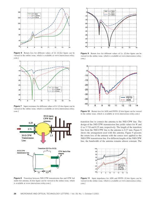
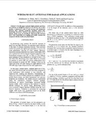
Figure 2 Return loss <strong>for</strong> different values of d1. [Color figure can beviewed in the online issue, which is available at www.interscience.wiley.com.]with width W and gap G equal to 2.5 and 1 mm, respectively. Theother dimensions are given in Table 1.3. SIMULATION AND RESULTSThe related simulation and analysis are per<strong>for</strong>med using AgilentTechnologies’ commercial computer software package, AdvancedDesign System (ADS), which is based on the method of moments(MoM) technique <strong>for</strong> layered media. The ADS simulator, calledMomentum, solves mixed potential integral equations (MPIE)using full-wave Green’s functions [4]. The design shown in Figure1 was originally analyzed with d3 held constant at zero (that is,there is no extended tuning <strong>slot</strong>). With d3 held at zero and d2 heldat 1.5 mm, d1 was varied; the resultant return loss is shown inFigure 2. The return loss in Figure 2 shows that decreasing d1increases the resonant frequency, while it does not affect thebandwidth.Figure 3 shows the return loss when d3 and d1 are held at 0 and2.5 mm, respectively. These results show that the resonant frequencyand the bandwidth of the <strong>antenna</strong> are increased when d2 isdecreased. However, the return loss at the center frequenciesincreases as d2 is decreased.Next, while varying d3, d1 and d2 were held constant at 2.5 and1 mm, respectively. Increasing the tuning <strong>slot</strong> extension (d3)Figure 4 Return loss <strong>for</strong> different values of d3. [Color figure can beviewed in the online issue, which is available at www.interscience.wiley.com.]increased the return loss at the resonant frequency. The relatedresults are shown in Figure 4. However, extending d3 slightlyincreases the bandwidth and reduces the variation of the inputresistance across the bandwidth of operation of the <strong>antenna</strong>, asshown in Figure 5.Another way in which the operating bandwidth of the <strong>antenna</strong>could be adjusted is by controlling the length Lf (the length of theCPW feed line). Figures 6 and 7 show the return loss and inputresistance <strong>for</strong> different lengths of Lf, respectively. Clearly when Lfis reduced the bandwidth of the <strong>antenna</strong> shifts up with an increasein bandwidth. However, when Lf is increased the bandwidth shiftsdown with a decrease in total bandwidth. From Figure 6 a bandwidthof 50% centered at 10 GHz is achieved <strong>for</strong> Lf equal to 4 mm.The results in Figure 7 show that the input resistance exhibits lessvariation within the bandwidth of operation when Lf is increased.There<strong>for</strong>e, the shortest possible length of CPW feed should beused.Since any changes in the CPW feed line length affects theper<strong>for</strong>mance of the <strong>antenna</strong>, a method needs to be developed tofeed the <strong>antenna</strong> from sources with varying distances from the<strong>antenna</strong> feed point. This is necessary because it may not bepractical to feed the <strong>antenna</strong> at exactly that point. To accomplishthis, a 50 CPW transmission line is designed along with aFigure 3 Return loss <strong>for</strong> different values of d2. [Color figure can beviewed in the online issue, which is available at www.interscience.wiley.com.]Figure 5 Input resistance <strong>for</strong> different values of d3. [Color figure can beviewed in the online issue, which is available at www.interscience.wiley.com.]MICROWAVE AND OPTICAL TECHNOLOGY LETTERS / Vol. 39, No. 1, October 5 2003 25
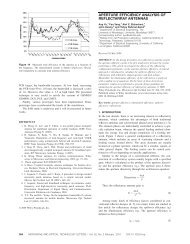
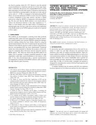
Figure 6 Return loss <strong>for</strong> different values of Lf. [Color figure can beviewed in the online issue, which is available at www.interscience.wiley.com.]Figure 9 Return loss <strong>for</strong> different values of Lc. [Color figure can beviewed in the online issue, which is available at www.interscience.wiley.com.]Figure 7 Input resistance <strong>for</strong> different values of Lf. [Color figure can beviewed in the online issue, which is available at www.interscience.wiley.com.]Figure 10 Return loss <strong>for</strong> ADS and FDTD. [Color figure can be viewedin the online issue, which is available at www.interscience.wiley.com.]transition line to connect the <strong>antenna</strong> to the 50 CPW line. Thedesign of the 50 CPW transmission line yields values <strong>for</strong> W andG as 5.718 and 0.25 mm, respectively. The length of the transitionline from the 50 CPW line to the <strong>antenna</strong> is 0.27 mm. Figure 8shows the arrangement used with this <strong>antenna</strong>. Figure 9 presentsthe return loss of the <strong>antenna</strong> with the source now applied to the50 CPW transmission line. For different lengths of the 50 CPWline, the bandwidth of the <strong>antenna</strong> remains almost constant. TheFigure 8 Transition between 50 CPW transmission line and CPW <strong>fed</strong><strong>multi</strong>-<strong>slot</strong> <strong>antenna</strong>. [Color figure can be viewed in the online issue, whichis available at www.interscience.wiley.com.]Figure 11 Input impedance <strong>for</strong> ADS and FDTD. [Color figure can beviewed in the online issue, which is available at www.interscience.wiley.com.]26 MICROWAVE AND OPTICAL TECHNOLOGY LETTERS / Vol. 39, No. 1, October 5 2003