XGSF-BS35(53)03-20 SFP BIDI 155M 1310/1550nm(1550/1310nm ...
XGSF-BS35(53)03-20 SFP BIDI 155M 1310/1550nm(1550/1310nm ...
XGSF-BS35(53)03-20 SFP BIDI 155M 1310/1550nm(1550/1310nm ...

You also want an ePaper? Increase the reach of your titles
YUMPU automatically turns print PDFs into web optimized ePapers that Google loves.
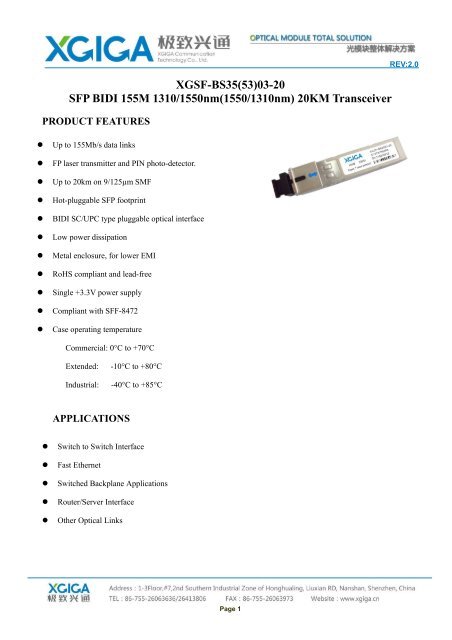
<strong>XGSF</strong>-<strong>BS35</strong>(<strong>53</strong>)<strong>03</strong>-<strong>20</strong><strong>SFP</strong> <strong>BIDI</strong> <strong>155M</strong> <strong>1310</strong>/<strong><strong>1550</strong>nm</strong>(<strong>1550</strong>/<strong>1310</strong>nm) <strong>20</strong>KM TransceiverPRODUCT FEATURES• Up to <strong>155M</strong>b/s data links• FP laser transmitter and PIN photo-detector.• Up to <strong>20</strong>km on 9/125µm SMF• Hot-pluggable <strong>SFP</strong> footprint• <strong>BIDI</strong> SC/UPC type pluggable optical interface• Low power dissipation• Metal enclosure, for lower EMI• RoHS compliant and lead-free• Single +3.3V power supply• Compliant with SFF-8472• Case operating temperatureCommercial: 0°C to +70°CREV:2.0Extended:Industrial:-10°C to +80°C-40°C to +85°CAPPLICATIONS• Switch to Switch Interface• Fast Ethernet• Switched Backplane Applications• Router/Server Interface• Other Optical LinksPage 1
REV:2.0PRODUCT DESCRIPTIONXGIGA’s <strong>XGSF</strong>-<strong>BS35</strong>(<strong>53</strong>)<strong>03</strong>-<strong>20</strong> Small Form Factor Pluggable (<strong>SFP</strong>) transceivers are compatible with theSmall Form Factor Pluggable Multi-Sourcing Agreement (MSA), The transceiver consists of four sections: the LDdriver, the limiting amplifier, the FP laser and the PIN photo-detector. The module data link up to <strong>20</strong>KM in9/125um single mode fiber.The optical output can be disabled by a TTL logic high-level input of Tx Disable, and the system also can disablethe module via I2C. Tx Fault is provided to indicate that degradation of the laser. Loss of signal (LOS) output isprovided to indicate the loss of an input optical signal of receiver or the link status with partner. The system canalso get the LOS (or Link)/Disable/Fault information via I2C register access.Ordering informationProduct part NumberDataRate(Mbps)<strong>XGSF</strong>-<strong>BS35</strong>(<strong>53</strong>)<strong>03</strong>-<strong>20</strong> 155<strong>XGSF</strong>-<strong>BS35</strong>(<strong>53</strong>)<strong>03</strong>-<strong>20</strong>E 155<strong>XGSF</strong>-<strong>BS35</strong>(<strong>53</strong>)<strong>03</strong>-<strong>20</strong>A <strong>155M</strong>ediaSingle modefiberSingle modefiberSingle modefiberWavelength(nm)TransmissionDistance(km)Temperature Range(Tcase)(℃)<strong>1310</strong>/<strong>1550</strong>(<strong>1550</strong>/<strong>1310</strong>) <strong>20</strong> 0~70 commercial<strong>1310</strong>/<strong>1550</strong>(<strong>1550</strong>/<strong>1310</strong>) <strong>20</strong> -10~80 extended<strong>1310</strong>/<strong>1550</strong>(<strong>1550</strong>/<strong>1310</strong>) <strong>20</strong> -40~85 industrialPage 2
REV:2.0Ⅰ.Pin DescriptionsPin Symbol Name/Description Ref.1 VEET Transmitter Ground (Common with Receiver Ground) 12 TFAULT Transmitter Fault.3 TDIS Transmitter Disable. Laser output disabled on high or open. 24 MOD_DEF(2) Module Definition 2. Data line for Serial ID. 35 MOD_DEF(1) Module Definition 1. Clock line for Serial ID. 36 MOD_DEF(0) Module Definition 0. Grounded within the module. 37 Rate Select No connection required 48 LOS Loss of Signal indication. Logic 0 indicates normal operation. 59VEERReceiver Ground (Common with Transmitter Ground) 110 VEER Receiver Ground (Common with Transmitter Ground) 111 VEER Receiver Ground (Common with Transmitter Ground) 112 RD- Receiver Inverted DATA out. AC Coupled13 RD+ Receiver Non-inverted DATA out. AC Coupled14 VEER Receiver Ground (Common with Transmitter Ground) 115 VCCR Receiver Power Supply16 VCCT Transmitter Power Supply17 VEET Transmitter Ground (Common with Receiver Ground) 118 TD+ Transmitter Non-Inverted DATA in. AC Coupled.19 TD- Transmitter Inverted DATA in. AC Coupled.<strong>20</strong> VEET Transmitter Ground (Common with Receiver Ground) 1Notes:1. Circuit ground is internally isolated from chassis ground.2. Laser output disabled on T DIS >2.0V or open, enabled on T DIS 30kΩresistor. The input states are:Low (0 – 0.8V): Reduced Bandwidth(> 0.8 V < 2.0V): UndefinedHigh (2.0 – 3.465V): Full BandwidthOpen:Reduced Bandwidth5. LOS is open collector output. Should be pulled up with 4.7k - 10kohms on host board to a voltagebetween 2.0V and 3.6V. Logic 0 indicates normal operation; logic 1 indicates loss of signal.Page 3
REV:2.0Figure 2: Pin out of Connector Block on Host BoardII. Absolute Maximum RatingsParameter Symbol Min. Typ. Max. Unit NoteStorage Temperature Ts -40 85 ºCStorage Ambient Humidity HA 5 95 %Power Supply Voltage VCC -0.5 4 VSignal Input Voltage -0.3 Vcc+0.3 VReceiver Damage Threshold 5 dBmIII. Recommended Operating ConditionsParameter Symbol Min. Typ. Max. Unit Note0 70 <strong>XGSF</strong>-<strong>BS35</strong>(<strong>53</strong>)<strong>03</strong>-<strong>20</strong>Case Operating Temperature Tcase -10 80 ºC <strong>XGSF</strong>-<strong>BS35</strong>(<strong>53</strong>)<strong>03</strong>-<strong>20</strong>E-40 85<strong>XGSF</strong>-<strong>BS35</strong>(<strong>53</strong>)<strong>03</strong>-<strong>20</strong>AAmbient Humidity HA 5 70 % Non-condensingPower Supply Voltage VCC 3.13 3.3 3.47 VPower Supply Current ICC 280 mAPower Supply Noise Rejection 100 mVp-p 100Hz to 1MHzData Rate 155/155 Mbps TX Rate/RX RateTransmission Distance <strong>20</strong> KMCoupled Fiber Single mode fiber 9/125um SMFPage 4
REV:2.0Ⅳ.Specification of TransmitterParameter Symbol Min. Typ. Max. Unit NoteAverage Output Power POUT -15 -8 dBmExtinction Ratio ER 8.2 dB1270 <strong>1310</strong> 1360 <strong>XGSF</strong>-<strong>BS35</strong><strong>03</strong>-<strong>20</strong>Center WavelengthλCnm1<strong>53</strong>0 <strong>1550</strong> 1570<strong>XGSF</strong>-BS<strong>53</strong><strong>03</strong>-<strong>20</strong>Spectrum Width (RMS) σ 3.5 nmFP LaserTransmitter OFF Output Power POff -45 dBmDifferential Line Input Impedance RIN 90 100 110 OhmTotal Jitter (Peak-Peak) tJ 1 ns Note (1)Output Eye Mask Compliant with G.957(class 1 laser safety)Note (2)Note (1): Measure at 2^23-1 NRZ PRBS patternNote (2): Transmitter eye mask definitionV. Specification of ReceiverParameter Symbol Min. Typ. Max. Unit NoteInput Optical WavelengthλIN1<strong>53</strong>0 <strong>1550</strong> 1570 <strong>XGSF</strong>-<strong>BS35</strong><strong>03</strong>-<strong>20</strong>nm1270 <strong>1310</strong> 1360<strong>XGSF</strong>-BS<strong>53</strong><strong>03</strong>-<strong>20</strong>Receiver Sensitivity PIN -29 dBm Note (1)Input Saturation Power (Overload) PSAT -8 dBmLos Of Signal Assert PA -38 dBmLos Of Signal De-assert PD -30 dBm Note (2)LOS Hysteresis PA-PD 0.5 2 6 dBNote (1): Measured with Light source <strong><strong>1550</strong>nm</strong> (<strong>1310</strong>nm), ER=9dB; BER =
REV:2.0VI. Electrical Interface CharacteristicsParameter Symbol Min. Typ. Max. Unit NoteTransmitterTotal Supply Current ICC A mA Note (1)Transmitter Disable Input-High VDISH 2 Vcc+0.3 VTransmitter Disable Input-Low VDISL 0 0.8 VTransmitter Fault Input-High VDISL 2 Vcc+0.3 VTransmitter Fault Input-Low VTxFH 0 0.8 VReceiverTotal Supply Current ICC B mA Note (1)LOSS Output Voltage-High VLOSH 2 Vcc+0.3 VLOSS Output Voltage-Low VLOSL 0 0.8 VLVTTLNote (1): A (TX) + B (RX) = 280mA(Not include termination circuit)VII. Recommend Circuit SchematicProtocol VccVCC3.3V10uFRES10.1uF1uH1uH10uFVccT0.1uFXGIGA <strong>SFP</strong> Module10KTx_DisableTx_FaultTx_DisableTx_FaultTD+0.1uFTD-VeeT100 Ohm0.1uFLaser DriverLaser DiodeVccRSerDes ICRES110uF0.1uFProtocol ICRD+0.1uF100 OhmAmplifierRD-0.1uFPhoto DiodeRx_LOSRx_LOS3.3VVeeRRES1RES1RES1PLD/PALMod_def 2Mod_def 1Mod_def 0EEPROMRES1=4.7K to10K Ohms* Depands onSerDes IC usedPage 6
REV:2.0VIII. Mechanical Specifications (Unit: mm)X Regulatory Compliance<strong>XGSF</strong>-<strong>BS35</strong>(<strong>53</strong>)<strong>03</strong>-<strong>20</strong>Feature Reference PerformanceElectrostatic discharge(ESD) IEC/EN 61000-4-2 Compatible with standardsElectromagnetic Interference (EMI)Laser Eye SafetyFCC Part 15 Class B EN 55022 Class B(CISPR 22A)FDA 21CFR 1040.10, 1040.11 IEC/EN60825-1,2Compatible with standardsClass 1 laser productComponent Recognition IEC/EN 60950 ,UL Compatible with standardsROHS <strong>20</strong>02/95/EC Compatible with standardsEMC EN61000-3 Compatible with standardsAppendix A. Document RevisionVersion No. Date Description1.0 <strong>20</strong>10-9-1 Preliminary datasheet2.0 <strong>20</strong>11-9-10 Update format and company’s logoPage 7