Semiconductor Crystals - Physics Department - University College ...
Semiconductor Crystals - Physics Department - University College ...
Semiconductor Crystals - Physics Department - University College ...

Create successful ePaper yourself
Turn your PDF publications into a flip-book with our unique Google optimized e-Paper software.
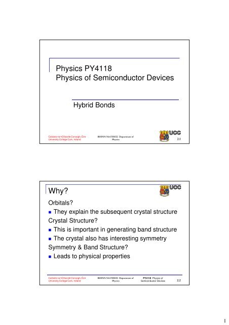
<strong>Physics</strong> PY4118<strong>Physics</strong> of <strong>Semiconductor</strong> DevicesHybrid BondsColáiste na hOllscoile Corcaigh, ÉireROINN NA FISICE <strong>Department</strong> of<strong>University</strong> <strong>College</strong> Cork, Ireland <strong>Physics</strong>2.1Why?Orbitals? They explain the subsequent crystal structureCrystal Structure? This is important in generating band structure The crystal also has interesting symmetrySymmetry & Band Structure? Leads to physical propertiesColáiste na hOllscoile Corcaigh, Éire<strong>University</strong> <strong>College</strong> Cork, IrelandROINN NA FISICE <strong>Department</strong> of PY4118 <strong>Physics</strong> of<strong>Physics</strong> <strong>Semiconductor</strong> Devices 2.21
Hybrid Orbitals One might expect the number of bonds formed by anatom would equal its unpaired electrons Chlorine, for example, generally forms one bond as it hasone unpaired electron - 1s 2 2s 2 2p 5 Oxygen, with two unpaired electrons, usually forms twobonds - 1s 2 2s 2 2p 4 However, Carbon, with only two unpaired electrons,generally forms four (4) bondsC (1s 2 2s 2 2p 2 ) [He] 2s 2 2p 2The four bonds come from the 2 (2s) paired electronsand the 2 (2p) unpaired electronsColáiste na hOllscoile Corcaigh, ÉireROINN NA FISICE <strong>Department</strong> of PY4118 <strong>Physics</strong> of<strong>University</strong> <strong>College</strong> Cork, Ireland <strong>Physics</strong><strong>Semiconductor</strong> Devices 2.3Hybrid Orbitals Linus Pauling proposed that the valence atomic orbitals ina molecule are different from those of the isolated atomsforming the molecule Quantum mechanical computations show that if specificcombinations of orbitals are mixed mathematically,“new” atomic orbitals are obtained The spatial orientation of these new orbitals lead to more“stable” bonds and are consistent with observedmolecular shapes These new orbitals are called: “Hybrid Orbitals”Coláiste na hOllscoile Corcaigh, ÉireROINN NA FISICE <strong>Department</strong> of PY4118 <strong>Physics</strong> of<strong>University</strong> <strong>College</strong> Cork, Ireland <strong>Physics</strong><strong>Semiconductor</strong> Devices 2.42
Hybrid Orbitals Types of Hybrid OrbitalsEach type has a unique geometric arrangementThe hybrid type is derived from the number of s, p, datomic orbitals used to form the HybridHybrid Orbitals(Hybridization)GeometricArrangementsNumber of HybridOrbitalsFormed byCentral AtomExamplesp Linear 2 Be in BeF 2sp 2 Trigonal planar 3 B in BF 3sp 3 Tetrahedral 4 C in CH 4Coláiste na hOllscoile Corcaigh, ÉireROINN NA FISICE <strong>Department</strong> of PY4118 <strong>Physics</strong> of<strong>University</strong> <strong>College</strong> Cork, Ireland <strong>Physics</strong><strong>Semiconductor</strong> Devices 2.5sp Hybrid Orbitals SP Hybridization 2 electron groups surround central atom Linear shape, 180 o apart VB theory proposes the mixing of two nonequivalentorbitals, one “s” and one “p”, to form two equivalent“sp” hybrid orbitals Orientation of hybrid orbitals extend electron densityin the bonding direction Minimizes repulsions between electrons Both shape and orientation maximize overlap betweenthe atomsColáiste na hOllscoile Corcaigh, ÉireROINN NA FISICE <strong>Department</strong> of PY4118 <strong>Physics</strong> of<strong>University</strong> <strong>College</strong> Cork, Ireland <strong>Physics</strong><strong>Semiconductor</strong> Devices 2.63
“sp” Hybrid OrbitalsEx: BeCl 2The Be-Cl bonds in BeCl 2 are neitherspherical (s orbitals) nor dumbbell (porbitals)The Be-Cl bonds have a hybrid shapeIn the Beryllium atom the 2s orbitaland one of the 2p orbitals mix to form2 sp hybrid orbitalsEach Be Hybrid sp orbital overlaps aChlorine 3p orbital in BeCl 2hybridorbitalsBeryllium Hybrid Orbital Diagramorbital box diagramsColáiste na hOllscoile Corcaigh, ÉireROINN NA FISICE <strong>Department</strong> of PY4118 <strong>Physics</strong> of<strong>University</strong> <strong>College</strong> Cork, Ireland <strong>Physics</strong><strong>Semiconductor</strong> Devices 2.7“sp 2 ” Hybridization sp 2 - Trigonal Planar geometry (Central atom bonded to three ligands) The three bonds have equivalent hybridized shapes The sp 2 hybridized orbitals are formed from:1 “s” orbital and 2 “p” orbitalsNote: Of the 4 orbitals available (1 s & 3 p) only the sorbital and 2 of the p orbitals are used to formhybrid orbitalsNote: Unlike electron configuration notation, hybridorbital notation uses superscripts for the number ofatomic orbitals of a given type that are mixed, NOT forthe number of electrons in the orbital, thus,sp 2 (3 orbitals), sp 3 (4 orbitals)Coláiste na hOllscoile Corcaigh, ÉireROINN NA FISICE <strong>Department</strong> of PY4118 <strong>Physics</strong> of<strong>University</strong> <strong>College</strong> Cork, Ireland <strong>Physics</strong><strong>Semiconductor</strong> Devices 2.84
“sp 2 ” HybridizationBF 3Hybrid Orbital DiagramThe 3 B-F bonds are neitherspherical nor dumbell shapedThey are all of identical shapeIn Boron, the “2s” orbital and two ofthe “2p” orbitals mix to form 3 sp 2hybrid orbitals, each containing onethe 3 total valence electronsBoron (B) 1s 2 2p 1Forms 3 sp 2 hybrid orbitalsEach of the Boron hybrid sp 2 orbitalsoverlaps with a 2p orbital of aFluorine atomBF 3Coláiste na hOllscoile Corcaigh, ÉireROINN NA FISICE <strong>Department</strong> of PY4118 <strong>Physics</strong> of<strong>University</strong> <strong>College</strong> Cork, Ireland <strong>Physics</strong><strong>Semiconductor</strong> Devices 2.9sp 3 Hybrid Orbitals sp 3 (4 bonds, thus, Tetrahedral geometry) The sp 3 hybridized orbitals are formed from:1 “s” orbital and 3 “p” orbitals Example”Carbon is the basis for “Organic Chemistry”Carbon is in group 4 of the Periodic Chart and has 4 valenceelectrons – 2s 2 2p 2The hybridization of these 4 electrons is critical in the formationof the many millions of organic compounds and as the basis oflife as we know itColáiste na hOllscoile Corcaigh, ÉireROINN NA FISICE <strong>Department</strong> of PY4118 <strong>Physics</strong> of<strong>University</strong> <strong>College</strong> Cork, Ireland <strong>Physics</strong><strong>Semiconductor</strong> Devices 2.105
sp 3 Hybrid Orbitals2p2pEnergy2s1s2s1sThis structure impliesdifferent shapes andenergies for the “s” and“p” bonds in carboncompounds.Observations indicatethat all fours bonds areequivalentC atom (ground state) C atom (promoted)Coláiste na hOllscoile Corcaigh, ÉireROINN NA FISICE <strong>Department</strong> of PY4118 <strong>Physics</strong> of<strong>University</strong> <strong>College</strong> Cork, Ireland <strong>Physics</strong><strong>Semiconductor</strong> Devices 2.11Hybridization of Carbon in CH 44 sp 3 orbitals formed2psp 3sp 32sC-H bondsEnergy1s1s1sC atom(ground state)C atom(hybridized state)C atom(in CH 4 )Coláiste na hOllscoile Corcaigh, ÉireROINN NA FISICE <strong>Department</strong> of PY4118 <strong>Physics</strong> of<strong>University</strong> <strong>College</strong> Cork, Ireland <strong>Physics</strong><strong>Semiconductor</strong> Devices 2.126
Oxygen Atom Bonding in H 2 O2p4 sp 3 Hybridized OrbitalsEnergy1s2sOCentral Atom(ground state)Coláiste na hOllscoile Corcaigh, Éire<strong>University</strong> <strong>College</strong> Cork, Ireland1ssp 3TetrahedralO atom(hybridized state)1slonepairssp 3O atom(in H 2 O)O-HbondsROINN NA FISICE <strong>Department</strong> of PY4118 <strong>Physics</strong> of<strong>Physics</strong> <strong>Semiconductor</strong> Devices 2.13Spatial Arrangement ofsp 3 Hybrid OrbitalsShape of sp 3 hybrid orbitaldifferent than either s or pColáiste na hOllscoile Corcaigh, ÉireROINN NA FISICE <strong>Department</strong> of PY4118 <strong>Physics</strong> of<strong>University</strong> <strong>College</strong> Cork, Ireland <strong>Physics</strong><strong>Semiconductor</strong> Devices 2.147
sp 3 orbitals - details 1. sp 3 = ½ s - ½ p x - ½ p y + ½ p z 2. sp 3 = ½ s - ½ p x + ½ p y - ½ p z 3. sp 3 = ½ s + ½ p x - ½ p y - ½ p z 4. sp 3 = ½ s + ½ p x + ½ p y + ½ p zLinear Combination of Atomic OrbitalsScalar product:(n.sp 3 ; m.sp 3 ) = 0Coláiste na hOllscoile Corcaigh, ÉireROINN NA FISICE <strong>Department</strong> of PY4118 <strong>Physics</strong> of<strong>University</strong> <strong>College</strong> Cork, Ireland <strong>Physics</strong><strong>Semiconductor</strong> Devices 2.15Hybridization visualisation http://www.mhhe.com/physsci/chemistry/essentialchemistry/flash/hybrv18.swfColáiste na hOllscoile Corcaigh, Éire<strong>University</strong> <strong>College</strong> Cork, IrelandROINN NA FISICE <strong>Department</strong> of PY4118 <strong>Physics</strong> of<strong>Physics</strong> <strong>Semiconductor</strong> Devices 2.168
<strong>Physics</strong> PY4118<strong>Physics</strong> of <strong>Semiconductor</strong> Devices<strong>Semiconductor</strong> <strong>Crystals</strong>Coláiste na hOllscoile Corcaigh, ÉireROINN NA FISICE <strong>Department</strong> of<strong>University</strong> <strong>College</strong> Cork, Ireland <strong>Physics</strong>2.17<strong>Crystals</strong>The language used for crystals is required: To describe semiconductors To understand details of band structure To design certain types of devicesWill revisit during discussion on symmetryColáiste na hOllscoile Corcaigh, Éire<strong>University</strong> <strong>College</strong> Cork, IrelandROINN NA FISICE <strong>Department</strong> of PY4118 <strong>Physics</strong> of<strong>Physics</strong> <strong>Semiconductor</strong> Devices 2.189
Valence e ’ s for “main group” elementsColáiste na hOllscoile Corcaigh, Éire<strong>University</strong> <strong>College</strong> Cork, IrelandROINN NA FISICE <strong>Department</strong> of<strong>Physics</strong>PY4118 <strong>Physics</strong> of<strong>Semiconductor</strong> Devices2.19Group 4 <strong>Semiconductor</strong>s4 sp 3 orbitals formed3psp 3sp 3Energy2s3s3s 2 3p 22s3sSi-Si bondsSi atom(ground state)Si atom(hybridized state)Si crystalColáiste na hOllscoile Corcaigh, ÉireROINN NA FISICE <strong>Department</strong> of PY4118 <strong>Physics</strong> of<strong>University</strong> <strong>College</strong> Cork, Ireland <strong>Physics</strong><strong>Semiconductor</strong> Devices 2.2010
III-V <strong>Semiconductor</strong>s3 sp 3 orbitals formed4 sp 3 orbitals formedsp 3sp 3sp 3Si-Si bondsEnergy3s4s 2 4p 1 4s 2 4p 33s3sGa atom(hybridized state)As atom(hybridized state)GaAs crystalColáiste na hOllscoile Corcaigh, ÉireROINN NA FISICE <strong>Department</strong> of PY4118 <strong>Physics</strong> of<strong>University</strong> <strong>College</strong> Cork, Ireland <strong>Physics</strong><strong>Semiconductor</strong> Devices 2.21Zincblende (diamond structure)(two interpenetrating fcc lattices)What is fcc?Si, Ge, GaAs, InP, etc.Diamond: The 2 atoms are the same.Zincblende: The 2 atoms are different.Coláiste na hOllscoile Corcaigh, ÉireROINN NA FISICE <strong>Department</strong> of PY4118 <strong>Physics</strong> of<strong>University</strong> <strong>College</strong> Cork, Ireland <strong>Physics</strong><strong>Semiconductor</strong> Devices 2.2211
Zincblende (ZnS) Lattice View of tetrahedral coordination & 2 atom basis:Zincblende/Diamond≡ face centered cubic (fcc)lattice with a 2 atom basisColáiste na hOllscoile Corcaigh, ÉireROINN NA FISICE <strong>Department</strong> of PY4118 <strong>Physics</strong> of<strong>University</strong> <strong>College</strong> Cork, Ireland <strong>Physics</strong><strong>Semiconductor</strong> Devices 2.23Wurtzite (hexagonal structure)GaN, AlN etc. (semiconductors for blue lasers)Coláiste na hOllscoile Corcaigh, ÉireROINN NA FISICE <strong>Department</strong> of PY4118 <strong>Physics</strong> of<strong>University</strong> <strong>College</strong> Cork, Ireland <strong>Physics</strong><strong>Semiconductor</strong> Devices 2.2412
Wurtzite LatticeView of tetrahedral coordination& 2 atom basis.Wurtzite ≡ hexagonal closepacked (hcp) lattice,2 atom basisWhat does this mean?Coláiste na hOllscoile Corcaigh, ÉireROINN NA FISICE <strong>Department</strong> of PY4118 <strong>Physics</strong> of<strong>University</strong> <strong>College</strong> Cork, Ireland <strong>Physics</strong><strong>Semiconductor</strong> Devices 2.25Materials with sp 2 Hybridization What material is made with sp 2 ?Coláiste na hOllscoile Corcaigh, ÉireROINN NA FISICE <strong>Department</strong> of PY4118 <strong>Physics</strong> of<strong>University</strong> <strong>College</strong> Cork, Ireland <strong>Physics</strong><strong>Semiconductor</strong> Devices 2.2613
Survey of Solid State <strong>Physics</strong>Taken from: EP364 Solid State <strong>Physics</strong>Prof.Dr. Beşire GÖNÜLLink to full notes providedColáiste na hOllscoile Corcaigh, Éire<strong>University</strong> <strong>College</strong> Cork, IrelandROINN NA FISICE <strong>Department</strong> of PY4118 <strong>Physics</strong> of<strong>Physics</strong> <strong>Semiconductor</strong> Devices 2.27Crystalline SolidSingle crystal has an atomic structure that repeats periodicallyacross its whole volume. Even at infinite length scales, eachatom is related to every other equivalent atom in the structureby translational symmetrySingle PyriteCrystalSingle CrystalAmorphousSolidCrystal Structure 2814
Polycrystalline SolidPolycrystal is a material made up of an aggregate of many small single crystals(also called crystallites or grains).These regions are called as grains ( domain) and are separated from oneanother by grain boundaries. The atomic order can vary from one domain to thenext.The grains are usually 100 nm - 100 microns in diameter. Polycrystals withgrains that are
CRYSTAL LATTICEWhat is crystal (space) lattice?In crystallography, only the geometrical properties of the crystalare of interest, therefore one replaces each atom by ageometrical point located at the equilibrium position of that atom.Platinum Platinum surface Crystal lattice andstructure of Platinum(scanning tunneling microscope)Crystal Structure 31Crystal Lattice An infinite array ofpoints in space,Each point has identicalsurroundings to allothers.yBbOCαaADxE Arrays are arrangedexactly in a periodicmanner.Crystal Structure 3216
Crystal StructureCrystal structure can be obtained by attaching atoms, groupsof atoms or molecules which are called basis (motif) to thelattice sides of the lattice point.Crystal Structure = Crystal Lattice + BasisCrystal Structure 33A two-dimensional Bravais lattice withdifferent choices for the basis17
Types Of Crystal Lattices1) Bravais lattice is an infinite array of discrete points with anarrangement and orientation that appears exactly the same,from whichever of the points the array is viewed. Lattice isinvariant under a translation.Nb filmCrystal Structure 35Types Of Crystal Lattices2) Non-Bravais LatticeNot only the arrangement but also the orientation must appearexactly the same from every point in a bravais lattice.The red side has a neighbour to itsimmediate left, the blue one insteadhas a neighbour to its right.Red (and blue) sides are equivalentand have the same appearanceRed and blue sides are not equivalent.Same appearance can be obtainedrotating blue side 180º.HoneycombCrystal Structure 3618
Crystal LatticeBravais Lattice (BL)Non-Bravais Lattice (non-BL) All atoms are of the same kind All lattice points are equivalent Atoms can be of different kind Some lattice points are notequivalentA combination of two or more BLCrystal Structure 37Translational Lattice Vectors – 2DPA space lattice is a set of points such thata translation from any point in the latticeby a vector;R n = n 1 a + n 2 bPoint D(n1, n2) = (0,2)Point F (n1, n2) = (0,-1)locates an exactly equivalent point, i.e. apoint with the same environment as P .This is translational symmetry. Thevectors a, b are known as lattice vectorsand (n 1 , n 2 ) is a pair of integers whosevalues depend on the lattice point.Crystal Structure 3819
Lattice Vectors – 2DThe two vectors a and bform a set of lattice vectorsfor the lattice. The choice of latticevectors is not unique.Thus one could equally welltake the vectors a and b’ asa lattice vectors.Crystal Structure 39Lattice Vectors – 3DAn ideal three dimensional crystal is described by 3fundamental translation vectors a, b and c. If there is a latticepoint represented by the position vector r, there is then also alattice point represented by the position vector where u, v and ware arbitrary integers.r’ = r + u a + v b + w cCrystal Structure 4020
Unit Cell in 2DThe smallest component of the crystal (group of atoms, ionsor molecules), which when stacked together with puretranslational repetition reproduces the whole crystal.SSSSSbaSSSSSSSSSSCrystal Structure 41Unit Cell in 2DThe smallest component of the crystal (group of atoms, ionsor molecules), which when stacked together with puretranslational repetition reproduces the whole crystal.The choice ofunit cellis not unique.SSbSSaCrystal Structure 4221
2D Unit Cell example -(NaCl)We define lattice points ; these are points with identicalenvironmentsCrystal Structure 43Choice of origin is arbitrary - lattice points need not beatoms - but unit cell size should always be the same.Crystal Structure 4422
This is also a unit cell -it doesn’t matter if you start from Na or ClCrystal Structure 45- or if you don’t start from an atomCrystal Structure 4623
This is NOT a unit cell even though they are all thesame - empty space is not allowed!Crystal Structure 47Unit Cell in 3DCrystal Structure 4824
Three common Unit Cell in 3DCrystal Structure 49UNIT CELLPrimitive Single lattice point per cell Smallest area in 2D, orSmallest volume in 3DConventional & Non-primitive More than one lattice point per cell Integral multibles of the area ofprimitive cellSimple cubic(sc)Conventional = Primitive cellBody centered cubic(bcc)Conventional ≠ Primitive cellCrystal Structure 5025
The Conventional Unit Cell A unit cell just fills space whentranslated through a subset ofBravais lattice vectors. The conventional unit cell ischosen to be larger than theprimitive cell, but with the fullsymmetry of the Bravais lattice. The size of the conventional cell isgiven by the lattice constant a.Crystal Structure 51Primitive and conventional cells of FCCCrystal Structure 5226
Primitive and conventional cells-hcppoints of primitive cellHexagonal close packed cell (hcp):conventional =primitive cellcFractional coordinates:100, 010, 110, 101,011, 111,000, 001baCrystal Structure 53Primitive Unit Cell and vectorsA primitive unit cell is made of primitivetranslation vectors a 1 ,a 2 , and a 3 such thatthere is no cell of smaller volume that canbe used as a building block for crystalstructures.A primitive unit cell will fill space by repetitionof suitable crystal translation vectors. Thisdefined by the parallelpiped a 1 , a 2 and a 3 .The volume of a primitive unit cell can befound by V = a 1 .(a 2 x a 3 ) (vector products) Cubic cell volume = a 3Crystal Structure 5427
Primitive Unit CellThe primitive unit cell must have only one lattice point.There can be different choices for lattice vectors , but thevolumes of these primitive cells are all the same.a 1P = Primitive Unit CellNP = Non-Primitive Unit CellCrystal Structure 5528